16. Comparator (COMP)
16.1 Introduction
STM32L0x3 devices embed two ultra-low-power comparators COMP1, and COMP2 that can be used either as standalone devices (all terminal are available on I/Os) or combined with the timers.
The comparators can be used for a variety of functions including:
- • Wakeup from low-power mode triggered by an analog signal,
- • Analog signal conditioning,
- • Cycle-by-cycle current control loop when combined with the DAC and a PWM output from a timer.
16.2 COMP main features
- • COMP1 comparator with ultra low consumption
- • COMP2 comparator with rail-to-rail inputs, fast or slow mode
- • Each comparator has positive and configurable negative inputs used for flexible voltage selection:
- – I/O pins
- – DAC
- – Internal reference voltage and three submultiple values (1/4, 1/2, 3/4) provided by scaler (buffered voltage divider)
- • Programmable speed / consumption (COMP2 only)
- • The outputs can be redirected to an I/O or to timer inputs for triggering:
- – Capture events
- • COMP1, and COMP2 can be combined in a window comparator. Each comparator has interrupt generation capability with wakeup from Sleep and Stop modes (through the EXTI controller)
16.3 COMP functional description
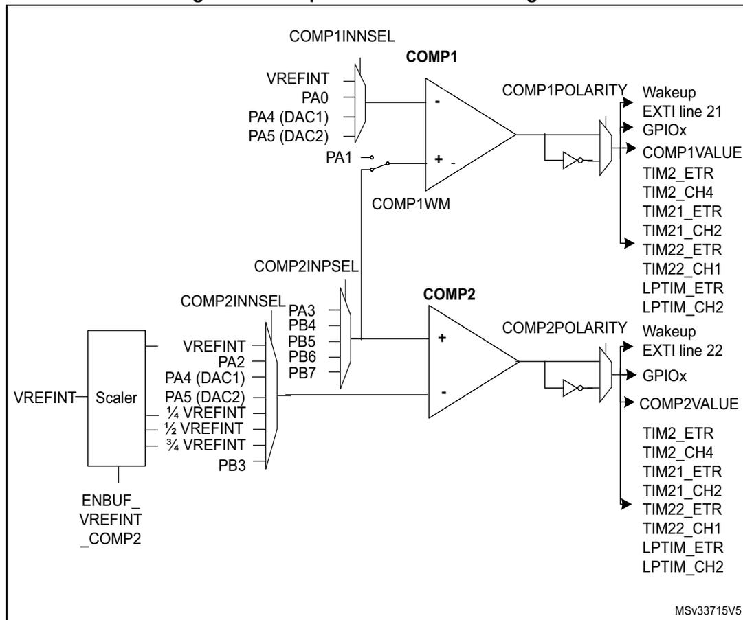
16.3.1 COMP block diagram
The block diagram of the comparators is shown in Figure 66: Comparator 1 and 2 block diagrams .
Figure 66. Comparator 1 and 2 block diagrams
16.3.2 COMP pins and internal signals
The I/Os used as comparators inputs must be configured in analog mode in the GPIOs registers.
The comparator output can be connected to the I/Os using the alternate function channel given in “Alternate function mapping” table in the datasheet.
The output can also be internally redirected to a variety of timer input for the following purposes:
- • Input capture for timing measures
It is possible to have the comparator output simultaneously redirected internally and externally.
16.3.3 COMP reset and clocks
The COMP clock provided by the clock controller is synchronous with the PCLK (APB clock).
There is no clock enable control bit provided in the RCC controller. Reset and clock enable bits are common for COMP and SYSCFG.
Important: The polarity selection logic and the output redirection to the port works independently from the PCLK clock. This allows the comparator to work even in Stop mode.
16.3.4 Comparator LOCK mechanism
The comparators can be used for safety purposes, such as over-current or thermal protection. For applications having specific functional safety requirements, it is necessary to insure that the comparator programming cannot be altered in case of spurious register access or program counter corruption.
For this purpose, the comparator control and status registers can be write-protected (read-only).
Once the programming is completed, the COMPx LOCK bit can be set to 1. This causes the whole COMPx_CSR register to become read-only, including the COMPx LOCK bit.
The write protection can only be reset by a MCU reset.
16.3.5 Power mode
COMP2 power consumption versus propagation delay can be adjusted to have the optimum trade-off for a given application.
COMP2_SPEED bit in the COMP2_CSR register can be programmed to provide either higher speed/consumption or lower speed/consumption.
16.4 COMP interrupts
The comparator outputs are internally connected to the Extended interrupts and events controller. Each comparator has its own EXTI line and can generate either interrupts or events. The same mechanism is used to exit from low-power modes.
Refer to Interrupt and events section for more details.
16.5 COMP registers
16.5.1 Comparator 1 control and status register (COMP1_CSR)
The COMP1_CSR is the Comparator1 control/status register. It contains all the bits /flags related to comparator1.
Address offset: 0x18
System reset value: 0x0000 0000
| 31 | 30 | 29 | 28 | 27 | 26 | 25 | 24 | 23 | 22 | 21 | 20 | 19 | 18 | 17 | 16 |
|---|---|---|---|---|---|---|---|---|---|---|---|---|---|---|---|
| COMP1 LOCK | COMP1 VALUE | Res. | Res. | Res. | Res. | Res. | Res. | Res. | Res. | Res. | Res. | Res. | Res. | Res. | Res. |
| rs | r |
| 15 | 14 | 13 | 12 | 11 | 10 | 9 | 8 | 7 | 6 | 5 | 4 | 3 | 2 | 1 | 0 |
|---|---|---|---|---|---|---|---|---|---|---|---|---|---|---|---|
| COMP1 POLARITY | Res. | Res. | COMP1 LPTIMIN1 | Res. | Res. | Res. | COMP1 WM | Res. | Res. | COMP1INN SEL | Res. | Res. | Res. | COMP1 EN | |
| rw | rw | rw | rw rw | rw | |||||||||||
Bit 31 COMP1LOCK : COMP1_CSR register lock bit
This bit is set by software and cleared by a hardware system reset. It locks the whole content of the comparator 1 control register, COMP1_CSR[31:0]
0: COMP1_CSR[31:0] for comparator 1 are read/write
1: COMP1_CSR[31:0] for comparator 1 are read-only
Bit 30 COMP1VALUE : Comparator 1 output status bit
This bit is read-only. It reflects the current comparator 1 output taking into account COMP1POLARITY bit effect.
Bits 29:16 Reserved, must be kept at reset value
Bit 15 COMP1POLARITY : Comparator 1 polarity selection bit
This bit is set and cleared by software (only if COMP1LOCK not set). It inverts Comparator 1 polarity.
0: Comparator 1 output value not inverted
1: Comparator 1 output value inverted
Bits 14:13 Reserved, must be kept at reset value
Bit 12 COMP1LPTIMIN1 : Comparator 1 LPTIM input propagation bit
This bit is set and cleared by software (assuming COMP1LOCK not set). It sends COMP1VALUE to LPTIM input 1.
0: Comparator 1 output gated
1: Comparator 1 output sent to LPTIM input 1
Bits 11:9 Reserved, must be kept at reset value
Bit 8 COMP1WM : Comparator 1 window mode selection bit
This bit is set and cleared by software (only if COMP1LOCK not set). It selects comparator 1 window mode where the Plus inputs of both comparators are connected together.
0: Plus input of comparator 1 connected to PA1.
1: Plus input of comparator 1 shorted with Plus input of comparator 2 (see COMP1_CSR).
Bits 7:6 Reserved, must be kept at reset value
Bits 5:4 COMP1INNSE : Comparator 1 Input Minus connection configuration bit
These bits are set and cleared by software (only if COMP1LOCK not set). They select which input is connected with the Input Minus of comparator 1
00: VREFINT
01: PA0
10: DAC1/PA4
11: DAC2/PA5
Bits 3:1 Reserved, must be kept at reset value
Bit 0 COMP1EN : Comparator 1 enable bit
This bit is set and cleared by software (only if COMP1LOCK not set). It switches on comparator1
0: Comparator 1 switched OFF.
1: Comparator 1 switched ON.
16.5.2 Comparator 2 control and status register (COMP2_CSR)
The COMP2_CSR is the Comparator2 control/status register. It contains all the bits /flags related to comparator2.
Address offset: 0x1C
System reset value: 0x0000 0000
| 31 | 30 | 29 | 28 | 27 | 26 | 25 | 24 | 23 | 22 | 21 | 20 | 19 | 18 | 17 | 16 |
|---|---|---|---|---|---|---|---|---|---|---|---|---|---|---|---|
| COMP2 LOCK | COMP2 VALUE | Res. | Res. | Res. | Res. | Res. | Res. | Res. | Res. | Res. | Res. | Res. | Res. | Res. | Res. |
| rs | r | ||||||||||||||
| 15 | 14 | 13 | 12 | 11 | 10 | 9 | 8 | 7 | 6 | 5 | 4 | 3 | 2 | 1 | 0 |
| COMP2 POLARITY | Res. | COMP2 LPTIMIN1 | COMP2 LPTIMIN2 | Res. | COMP2INPSEL | Res. | COMP2INNSE | COMP2 SPEED | Res. | Res. | COMP2 EN | ||||
| rw | rw | rw | rw | rw | rw | rw | rw | rw | rw | rw | |||||
Bit 31 COMP2LOCK : COMP2_CSR register lock bit
This bit is set by software and cleared by a hardware system reset. It locks the whole content of the comparator 2 control register, COMP2_CSR[31:0]
0: COMP2_CSR[31:0] for comparator 1 are read/write
1: COMP2_CSR[31:0] for comparator 1 are read-only
Bit 30 COMP2VALUE : Comparator 2 output status bit
This bit is read-only. It reflects the current comparator 2 output taking into account COMP2POLARITY bit effect.
Bits 29:16 Reserved, must be kept at reset value
Bit 15 COMP2POLARITY : Comparator 2 polarity selection bit
This bit is set and cleared by software (only if COMP2LOCK not set). It inverts Comparator 1 polarity.
0: Comparator 2 output value not inverted
1: Comparator 2 output value inverted
Bit 14 Reserved, must be kept at reset value
Bit 13 COMP2LPTIMIN1 : Comparator 2 LPTIM input 1 propagation bit
This bit is set and cleared by software (assuming COMP2LOCK not set). It sends COMP2VALUE to LPTIM input 1.
0: Comparator 2 output gated
1: Comparator 2 output sent to LPTIM input 1
Note: COMP2LPTIMIN1 and COMP2LPTIMIN2 cannot both be set to '1'.
Bit 12 COMP2LPTIMIN2 : Comparator 2 LPTIM input 2 propagation bit
This bit is set and cleared by software (assuming COMP2LOCK not set). It sends COMP2VALUE to LPTIM input 2.
0: Comparator 2 output gated
1: Comparator 2 output sent to LPTIM input 2
Note: COMP2LPTIMIN1 and COMP2LPTIMIN2 cannot both be set to '1'.
Bit 11 Reserved, must be kept at reset value
Bits 10:8 COMP2INPSEL : Comparator 2 Input Plus connection configuration bit
These bits are set and cleared by software (only if COMP2LOCK not set). They select which input is connected with the Input Plus of comparator 2
000: PA3
001: PB4
010: PB5
011: PB6
100: PB7
Others: Reserved.
Bit 7 Reserved, must be kept at reset value
Bits 6:4 COMP2INNSEL : Comparator 2 Input Minus connection configuration bit
These bits are set and cleared by software (only if COMP2LOCK not set). They select which input is connected with the Input Minus of comparator 2.
000: VREFINT
001: PA2
010: DAC /PA4
011: DAC2/PA5
100: 1/4 VREFINT
101: 1/2 VREFINT
110: 3/4 VREFINT
111: PB3
Note: If VREFINT or a fraction of VREFINT (using the scaler) is selected, then EN_VREFINT bit must be set in the SYSCFG_CFGR3 register (see Section 10.2.3: Reference control and status register (SYSCFG_CFGR3) ).
Bit 3 COMP2SPEED : Comparator 2 power mode selection bit
This bit is set and cleared by software (only if COMP2LOCK not set). It selects comparator 2 power mode.
0: slow speed
1: fast speed
Bits 2:1 Reserved, must be kept at reset value
Bit 0 COMP2EN : Comparator 2 enable bit
This bit is set and cleared by software (only if COMP2LOCK not set). It switches on comparator 2.
0: Comparator 2 switched off.
1: Comparator 2 switched ON.
16.5.3 COMP register map
The following table summarizes the comparator registers.
The comparator registers share SYSCFG peripheral register base addresses.
Table 72. COMP register map and reset values
| Offset | Register | 31 | 30 | 29 | 28 | 27 | 26 | 25 | 24 | 23 | 22 | 21 | 20 | 19 | 18 | 17 | 16 | 15 | 14 | 13 | 12 | 11 | 10 | 9 | 8 | 7 | 6 | 5 | 4 | 3 | 2 | 1 | 0 |
|---|---|---|---|---|---|---|---|---|---|---|---|---|---|---|---|---|---|---|---|---|---|---|---|---|---|---|---|---|---|---|---|---|---|
| 0x18 | COMP1_CSR | COMP1LOCK | COMP1VALUE | Res. | Res. | Res. | Res. | Res. | Res. | Res. | Res. | Res. | Res. | Res. | Res. | Res. | Res. | COMP1POLARITY | Res. | Res. | COMP1LPTMIN1 | Res. | Res. | Res. | COMP1WM | Res. | Res. | COMP1INNSSEL | Res. | Res. | Res. | Res. | COMP1EN |
| Reset value | 0 | 0 | 0 | 0 | 0 | 0 | 0 | 0 | |||||||||||||||||||||||||
| 0x1C | COMP2_CSR | COMP2LOCK | COMP2VALUE | Res. | Res. | Res. | Res. | Res. | Res. | Res. | Res. | Res. | Res. | Res. | Res. | Res. | Res. | COMP2POLARITY | Res. | COMP2LPTMIN1 | COMP2LPTMIN2 | Res. | COMP2INPSEL | Res. | Res. | Res. | COMP2INNSSEL | Res. | COMP2SPEED | Res. | Res. | COMP2EN | |
| Reset value | 0 | 0 | 0 | 0 | 0 | 0 | 0 | 0 | 0 | 0 |
Refer to Section 2.2 on page 58 for the register boundary addresses.