3. Flash program memory and data EEPROM (FLASH)
3.1 Introduction
The non-volatile memory (NVM) is composed of:
- • Up to 192 Kbytes of Flash program memory. This area is used to store the application code.
- • Up to 6 Kbytes of data EEPROM
- • An information block:
- – Up to 8 Kbytes of System memory
- – Up to 8x4 bytes of user Option bytes
- – Up to 96 bytes of factory Option bytes
3.2 NVM main features
The NVM interface features:
- • Read interface organized by word, half-word or byte in every area
- • Programming in the Flash memory performed by word or half-page
- • Programming in the Option bytes area performed by word
- • Programming in the data EEPROM performed by word, half-word or byte (granularity of the data EEPROM is one word, erase/write endurance cycles are linked to one word granularity)
- • Erase operation performed by page (in Flash memory, data EEPROM and Option bytes)
- • Option byte Loader
- • ECC (Error Correction Code): 6 bits stored for every word to recognize and correct just one error
- • Mass erase operation
- • Read / Write protection
- • PCROP protection
- • Low-power mode
- • Category 5 devices only:
- – Dual-bank memory with read-while-write
- – Dual-bank boot capability allowing to boot either from Bank 1 or Bank 2 at startup
- – Bank swapping capability.
3.3 NVM functional description
3.3.1 NVM organization
The NVM is organized as 32-bit memory cells that can be used to store code, data, boot code or Option bytes.
The memory array is divided into pages. A page is composed of 32 words (or 128 bytes) in Flash program memory and System memory, and 1 single word (or 4 bytes) in data EEPROM and Option bytes areas (user and factory). The erase/write endurance cycles are linked to one page granularity for Flash program memory and one single word granularity for data EEPROM.
A Flash sector is made of 32 pages (or 4 Kbytes). The sector is the granularity of the write protection.
Table 5. NVM organization (category 3 devices)
| NVM | NVM addresses | Size (bytes) | Name | Description |
|---|---|---|---|---|
| Flash program memory (1) | 0x0800 0000 - 0x0800 007F | 128 bytes | Page 0 | sector 0 |
| 0x0800 0080 - 0x0800 00FF | 128 bytes | Page 1 | ||
| - | - | - | ||
| 0x0800 0F80 - 0x0800 0FFF | 128 bytes | Page 31 | ||
| : | : | : | : | |
| 0x0800 7000 - 0x0800 707F | 128 bytes | Page 224 | sector 7 | |
| 0x0800 7080 - 0x0800 70FF | 128 bytes | Page 225 | ||
| - | - | - | ||
| 0x0800 7F80 - 0x0800 7FFF | 128 bytes | Page 255 | ||
| : | : | : | : | |
| 0x0800 F000 - 0x0800 F07F | 128 bytes | Page 480 | sector 15 | |
| 0x0800 F080 - 0x0800 F0FF | 128 bytes | Page 481 | ||
| - | - | - | ||
| 0x0800 FF80 - 0x0800 FFFF | 128 bytes | Page 511 | ||
| Data EEPROM | 0x0808 0000 - 0x0808 07FF | 2 Kbytes | - | Data EEPROM |
| Information block | 0x1FF0 0000 - 0x1FF0 0FFF | 4 Kbytes | - | System memory |
| 0x1FF8 0020 - 0x1FF8 007F | 96 bytes | - | Factory Options | |
| 0x1FF8 0000 - 0x1FF8 001F | 32 bytes | - | User Option bytes |
1. For 32 Kbyte category 3 devices, the Flash program memory is divided into 256 pages of 128 bytes each.
Table 6. NVM organization for UFB = 0 (192 Kbyte category 5 devices)
| NVM | NVM addresses | Size (bytes) | Name | Description | |
|---|---|---|---|---|---|
| Flash program memory | 0x0800 0000 - 0x0800 007F | 128 bytes | Page 0 | sector 0 | Bank 1 |
| 0x0800 0080 - 0x0800 00FF | 128 bytes | Page 1 | |||
| - | - | - | |||
| 0x0800 0F80 - 0x0800 0FFF | 128 bytes | Page 31 | |||
| . | . | . | . | ||
| . | . | . | . | ||
| . | . | . | . | ||
| 0x0800 7000 - 0x0800 707F | 128 bytes | Page 224 | sector 7 | ||
| 0x0800 7080 - 0x0800 70FF | 128 bytes | Page 225 | |||
| - | - | - | |||
| 0x0800 7F80 - 0x0800 7FFF | 128 bytes | Page 255 | |||
| . | . | . | . | ||
| . | . | . | . | ||
| . | . | . | . | ||
| - | - | - | |||
| 0x0801 7F80 - 0x0801 7FFF | 128 bytes | Page 767 | sector 23 | ||
| 0x0801 8000 - 0x0801 807F | 128 bytes | Page 768 | sector 24 | ||
| . | . | . | . | Bank 2 | |
| . | . | . | . | ||
| . | . | . | . | ||
| 0x0802 F000 - 0x0802 F07F | 128 bytes | Page 1504 | sector 47 | ||
| 0x0802 F080 - 0x0802 F0FF | 128 bytes | Page 1505 | |||
| - | - | - | |||
| 0x0802 FF80 - 0x0802 FFFF | 128 bytes | Page 1535 | |||
| Data EEPROM | 0x0808 0000 - 0x0808 0BFF | 6 Kbytes | - | Data EEPROM Bank 1 | |
| 0x0808 0C00 - 0x0808 17FF | - | Data EEPROM Bank 2 | |||
| Information block | 0x1FF0 0000 - 0x1FF0 1FFF | 8 Kbytes | - | System memory | |
| 0x1FF8 0020 - 0x1FF8 007F | 96 bytes | - | Factory Options | ||
| 0x1FF8 0000 - 0x1FF8 001F | 32 bytes | - | User Option bytes | ||
Table 7. Flash memory and data EEPROM remapping
(192 Kbyte category 5 devices)
| NVM | Description | NVM addresses | Remapped addresses | ||
|---|---|---|---|---|---|
| MEM_MODE = 0, BOOT0= 0 and UFB = 0 | MEM_MODE = 0, BOOT0= 0 and UFB = 1 | MEM_MODE = 0, BOOT0= 0 and UFB = 0 | MEM_MODE = 0, BOOT0= 0 and UFB = 1 | ||
| Flash program memory | Bank 1 | 0x0800 0000 - 0x0801 7FFF | 0x0801 8000 - 0x0802 FFFF | 0x0000 0000 - 0x0001 7FFF | 0x0001 8000 - 0x0002 FFFF |
| Bank 2 | 0x0801 8000 - 0x0802 FFFF | 0x0800 0000 - 0x0801 7FFF | 0x0001 8000 - 0x0002 FFFF | 0x0000 0000 - 0x0001 7FFF | |
| Data EEPROM | Bank 1 | 0x0808 0000 - 0x0808 0BFF | 0x0808 0C00 - 0x0808 17FF | 0x0008 0000 - 0x0008 0BFF | 0x0008 0C00 - 0x0008 17FF |
| Bank 2 | 0x0808 0C00 - 0x0808 17FF | 0x0808 0000 - 0x0808 0BFF | 0x0008 0C00 - 0x0008 17FF | 0x0008 0000 - 0x0008 0BFF | |
Table 8. NVM organization for UFB = 0 (128 Kbyte category 5 devices)
| NVM | NVM addresses | Size (bytes) | Name | Description | |
|---|---|---|---|---|---|
| Flash program memory | 0x0800 0000 - 0x0800 007F | 128 bytes | Page 0 | sector 0 | Bank 1 |
| 0x0800 0080 - 0x0800 00FF | 128 bytes | Page 1 | |||
| - | - | - | |||
| 0x0800 0F80 - 0x0800 0FFF | 128 bytes | Page 31 | |||
| . | . | . | . | ||
| . | . | . | . | ||
| . | . | . | . | ||
| 0x0800 7000 - 0x0800 707F | 128 bytes | Page 224 | sector 7 | ||
| 0x0800 7080 - 0x0800 70FF | 128 bytes | Page 225 | |||
| - | - | - | |||
| 0x0800 7F80 - 0x0800 7FFF | 128 bytes | Page 255 | |||
| . | . | . | . | ||
| . | . | . | . | ||
| . | . | . | . | ||
| 0x0800 FF80 - 0x0800 FFFF | 128 bytes | Page 511 | sector 15 | ||
| 0x0801 0000 - 0x0801 007F | 128 bytes | Page 512 | sector 16 | Bank 2 | |
| . | . | . | . | ||
| . | . | . | . | ||
| . | . | . | . | ||
| 0x0801 F000 - 0x0801 F07F | Page 992 | sector 31 | |||
| - | - | - | |||
| 0x0801 FF80 - 0x0801 FFFF | 128 bytes | Page 1023 | |||
| Data EEPROM | 0x0808 0000 - 0x0808 0BFF | 6 Kbytes | - | Data EEPROM Bank 1 | |
| 0x0808 0C00 - 0x0808 17FF | - | Data EEPROM Bank 2 | |||
Table 8. NVM organization for UFB = 0 (128 Kbyte category 5 devices) (continued)
| NVM | NVM addresses | Size (bytes) | Name | Description |
|---|---|---|---|---|
| Information block | 0x1FF0 0000 - 0x1FF0 1FFF | 8 Kbytes | - | System memory |
| 0x1FF8 0020 - 0x1FF8 007F | 96 bytes | - | Factory Options | |
| 0x1FF8 0000 - 0x1FF8 001F | 32 bytes | User Option bytes |
Table 9. Flash memory and data EEPROM remapping (128 Kbyte category 5 devices)
| NVM | Description | NVM addresses | Remapped addresses | ||
|---|---|---|---|---|---|
| MEM_MODE = 0, BOOT0= 0 and UFB = 0 | MEM_MODE = 0, BOOT0= 0 and UFB = 1 | MEM_MODE = 0, BOOT0= 0 and UFB = 0 | MEM_MODE = 0, BOOT0= 0 and UFB = 1 | ||
| Flash program memory | Bank 1 | 0x0800 0000 - 0x0800 FFFF | 0x0801 0000 - 0x0801 FFFF | 0x0000 0000 - 0x0000 FFFF | 0x0001 0000 - 0x0001 FFFF |
| Bank 2 | 0x0801 0000 - 0x0801 FFFF | 0x0800 0000 - 0x0800 FFFF | 0x0001 0000 - 0x0001 FFFF | 0x0000 0000 - 0x0000 FFFF | |
| Data EEPROM | Bank 1 | 0x0808 0000 - 0x0808 0BFF | 0x0808 0C00 - 0x0808 17FF | 0x0008 0000 - 0x0008 0BFF | 0x0008 0C00 - 0x0008 17FF |
| Bank 2 | 0x0808 0C00 - 0x0808 17FF | 0x0808 0000 - 0x0808 0BFF | 0x0008 0C00 - 0x0008 17FF | 0x0008 0000 - 0x0008 0BFF | |
Table 10. NVM organization for UFB = 0 (64 Kbyte category 5 devices) (1)
| NVM | NVM addresses | Size (bytes) | Name | Description | |
|---|---|---|---|---|---|
| Flash program memory | 0x0800 0000 - 0x0800 007F | 128 bytes | Page 0 | sector 0 | Bank 1 |
| 0x0800 0080 - 0x0800 00FF | 128 bytes | Page 1 | |||
| - | - | - | |||
| 0x0800 0F80 - 0x0800 0FFF | 128 bytes | Page 31 | |||
| . | . | . | sector 15 | ||
| . | . | . | |||
| . | . | . | |||
| 0x0800 F000 - 0x0800 F07F | 128 bytes | Page 480 | |||
| - | - | - | |||
| - | - | - | |||
| Data EEPROM | 0x0808 0C00 - 0x0808 17FF | 3 Kbytes | - | Data EEPROM Bank 2 | |
| Information block | 0x1FF0 0000 - 0x1FF0 1FFF | 8 Kbytes | - | System memory | |
| 0x1FF8 0020 - 0x1FF8 007F | 96 bytes | - | Factory Options | ||
| 0x1FF8 0000 - 0x1FF8 001F | 32 bytes | User Option bytes | |||
1. Flash memory and data EEPROM remapping is not possible on 64 Kbyte category 5 devices.
3.3.2 Dual-bank boot capability
Category 5 devices have two Flash memory banks: Bank 1 and Bank 2. They feature an additional boot mechanism which allows booting either from Bank 2 or from Bank 1 depending on BFB2 bit status (bit 23 in FLASH_OPTR register).
- • When the BFB2 bit is set and the boot pins are configured to boot from Flash memory (BOOT0 = 0 and BOOT1 = x), the device maps the System memory at address 0. It boots from the System memory after reset and Standby and executes (during approximately 440 µs) the embedded bootloader code which implements the dual-bank boot mechanism:
- a) The System memory code first checks Bank 2. If it contains a valid code (see note below), it sets the UFB bit in SYSCFG_CFGR1 register to map Bank 2 at address 0x0800 0000, jumps to the application code located in Bank 2, and leaves the bootloader.
- b) If the code located in Bank 2 is not valid, the System memory code checks Bank 1 code. If it is valid (see note below), it jumps to the application located in Bank 1 (UFB is kept at '0' so that Bank 1 remains mapped at address 0x0800 0000).
- c) If both Bank 2 and Bank 1 do not contain valid code (see note below), the normal bootloader operations are executed when the protection level2 is disabled. Otherwise, the System memory code jumps to Bank 1 regardless of its validity. Refer to Table 11 for more details.
- • When BFB2 bit is reset (default state), the dual-bank boot mechanism is not performed.
Note: The code is considered as valid when the first data located at the bank start address (which should be the stack pointer) points to a valid address (stack top address).
For category 5 devices, the Flash memory Bank 1 and Bank 2, System memory or SRAM can be selected as the boot area, as shown in Table 11 below.
Table 11. Boot pin and BFB2 bit configuration
| Protection level | BFB2 bit | Boot mode selection | Boot mode | Aliasing | |
|---|---|---|---|---|---|
| nBOOT1 option bit | BOOT0 pin | ||||
| 0 or 1 | 0 | X | 0 | User Flash memory | User Flash memory Bank1 is selected as the boot area. |
| 1 | 1 | System memory | Boot on System memory to execute bootloader. | ||
| 0 | 1 | Embedded SRAM | Boot on Embedded SRAM | ||
| 1 | X | 0 | System memory | Boot on System memory to execute dual bank boot mechanism. If Bank 2 and Bank 1 are not valid, bootloader is executed for Flash update. | |
| 1 | 1 | System memory | Boot on System memory to execute bootloader. | ||
| 0 | 1 | Embedded SRAM | Boot on Embedded SRAM. | ||
Table 11. Boot pin and BFB2 bit configuration (continued)
| Protection level | BFB2 bit | Boot mode selection | Boot mode | Aliasings | |
|---|---|---|---|---|---|
| nBOOT1 option bit | BOOT0 pin | ||||
| 2 | 0 | X | 0 | User Flash memory | User Flash memory Bank1 is selected as the boot area. |
| 1 | 1 | User Flash memory | |||
| 0 | 1 | User Flash memory | |||
| 1 | X | 0 | System memory | Boot on System memory to execute dual bank boot mechanism. If Bank 2 isn't valid, it jumps to Bank 1. | |
| 1 | 1 | System memory | |||
| 0 | 1 | System memory | |||
When entering System memory, you can either execute the bootloader (for Flash update) or execute Dual Bank Jump (see Table 11 ).
When protection level2 is enabled, the bootloader is never executed to perform a Flash update.
When the conditions a, b, and c described below are fulfilled, it is equivalent to configuring boot pins for System memory boot (BOOT0 = 1 and BOOT1 = 0). In this case when protection level2 is disabled, normal bootloader operations are executed.
- BFB2 bit is set.
- Both banks do not contain valid code.
- Boot pins configured as follows: BOOT0 = 0 and BOOT1 = x.
When the BFB2 bit is set, and Bank 2 and/or Bank 1 contain valid user application code, the Dual Bank Boot is always performed (bootloader always jumps to the user code).
Consequently, if you have set the BFB2 bit (to boot from Bank 2) then, to be able to execute the bootloader code for Flash update when protection level2 is disabled, you have to:
- Set the BFB2 bit to 0, BOOT0 = 1 and BOOT1 = 0 or,
- Program the content of address 0x0801 8000/0x0801 0000 (base address of Bank2) and 0x0800 0000 (base address of Bank1) to 0x0.
3.3.3 Reading the NVM
Protocol to read
To read the NVM content, take any address from Section 3.3.1: NVM organization . The clock of the memory interface must be running. (see MIFEN bit in Section 7.3.13: AHB peripheral clock enable register (RCC_AHBENR) ).
Depending on the clock frequency, a 0 or a 1 wait state can be necessary to read the NVM.
The user must set the correct number of wait states (LATENCY bit in the FLASH_ACR register). No control is done to verify if the frequency or the power used is correct, with respect to the number of wait states. A wrong number of wait states can generate wrong read values (high frequency and 0 wait states) or a long time to execute a code (low frequency with 1 wait state).
You can read the NVM by word (4 bytes), half-word (2 bytes) or byte.
When the NVM features only one bank, it is not possible to read the NVM during a write/erase operation. If a write/erase operation is ongoing, the reading will be in a wait state until the write/erase operation completes, stalling the master that requested the read operation, except when the address is read-protected. In this case, the error is sent to the master by a hard fault or a memory interface flag; no stall is generated and no read is waiting.
When two banks are available (category 5 devices), read operations from one bank can be performed while write or erase operations are performed on the other bank.
Relation between CPU frequency/Operation mode/NVM read time
The device (and the NVM) can work at different power ranges. For every range, some master clock frequencies can be set. Table 12 resumes the link between the power range and the frequencies to ensure a correct time access to the NVM.
Table 12. Link between master clock power range and frequencies
| Name | Power range | Maximum frequency (with 1 wait state) | Maximum frequency (without wait states) |
|---|---|---|---|
| Range 1 | 1.65 V - 1.95 V | 32 MHz | 16 MHz |
| Range 2 | 1.35 V - 1.65 V | 16 MHz | 8 MHz |
| Range 3 | 1.05 V - 1.35 V | 4.2 MHz | 4.2 MHz |
Table 13 shows the delays to read a word in the NVM. Comparing the complete time to read a word ( \( T_{total} \) ) with the clock period, you can see that in Range 3 no wait state is necessary, also with the maximum frequency (4.2 MHz) allowed by the device. \( T_{total} \) is the time that the NVM needs to return a value, and not the complete time to read it (from memory to Core through the memory interface); all remaining time is lost.
Table 13. Delays to memory access and number of wait states
| Name | \( T_{total} \) | Frequency | Period | Number of wait state required |
|---|---|---|---|---|
| Range 1 | 46.1 ns | 32 MHz | 31.25 | 1 |
| 16 MHz | 62.5 | 0 | ||
| Range 2 | 86.8 ns | 16 MHz | 62.5 | 1 |
| 8 MHz | 125 | 0 | ||
| Range 3 | 184.6 ns | 4 MHz | 250 | 0 |
| 2 MHz | 500 | 0 |
Change the CPU Frequency
After reset, the clock used is the MSI (2.1 MHz) and 0 wait state is configured in the FLASH_ACR register. The following software sequences have to be respected to tune the number of wait states needed to access the NVM with the CPU frequency.
A CPU clock or a number of wait state configuration changes may take some time before being effective. Checking the AHB prescaler factor and the clock source status values is a way to ensure that the correct CPU clock frequency is the configured one. Similarly, the read of FLASH_ACR is a way to ensure that the number of programmed wait states is effective.
Increasing the CPU frequency (in the same voltage range)
- 1. Program 1 wait state in LATENCY bit of FLASH_ACR register, if necessary.
- 2. Check that the new number of wait states is taken into account by reading the FLASH_ACR register. When the number of wait states changes, the memory interface modifies the way the read access is done to the NVM. The number of wait states cannot be modified when a read operation is ongoing, so the memory interface waits until no read is done on the NVM. If the master reads back the content of the FLASH_ACR register, this reading is stopped (and also the master which requested the reading) until the number of wait states is really changed. If the user does not read back the register, the following access to the NVM may be done with 0 wait states, even if the clock frequency has been increased, and consequently the values are wrong.
- 3. Modify the CPU clock source and/or the AHB clock prescaler in the Reset & Clock Controller (RCC).
- 4. Check that the new CPU clock source and/or the new CPU clock prescaler value is taken into account by reading respectively the clock source status and/or the AHB prescaler value in the Reset & Clock Controller (RCC). This check is important as some clocks may take time to get available.
For code example, refer to A.2.1: Increasing the CPU frequency preparation sequence code , A.2.3: Switch from PLL to HSI16 sequence code and A.2.4: Switch to PLL sequence code .
Decreasing the CPU frequency (in the same voltage range)
- 1. Modify the CPU clock source and/or the AHB clock prescaler in the Reset & Clock Controller (RCC).
- 2. Check that the new CPU clock source and/or the new CPU clock prescaler value is taken into account by reading respectively the clock source status and/or the AHB prescaler value in the Reset and Clock Controller (RCC).
- 3. Program 0 wait state in LATENCY bit of the FLASH_ACR register, if needed.
- 4. Check that the new number of wait states is taken into account by reading FLASH_ACR. It is necessary to read back the register for the reasons explained in the previous paragraph.
Data buffering
In the NVM, six buffers can impact the performance (and in some conditions help to reduce the power consumption) during read operations, both for fetch and data. The structure of one buffer is shown on Figure 3 .
Figure 3. Structure of one internal buffer
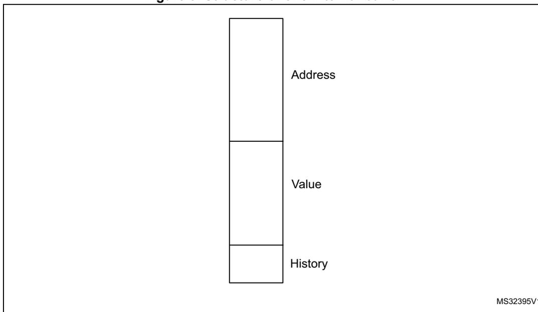
The diagram illustrates the internal structure of a buffer. It consists of three vertically stacked rectangular boxes. The top box is labeled 'Address' to its right. The middle box is labeled 'Value' to its right. The bottom box is labeled 'History' to its right. In the bottom right corner of the diagram area, the text 'MS32395V1' is present.
Each buffer stores 3 different types of information: address, data and history. In a read operation, if the address is found, the memory interface can return data without accessing the NVM. Data in the buffer is 32 bit wide (even if the master only reads 8 or 16 bits), so that a value can be returned whatever the size used in a previous reading. The history is used to know if the content of a buffer is valid and to delete (with a new value) the older one.
The buffers are used to store the value received by the NVM during normal read operations, and for speculative readings. Disabling the speculative reading makes that only the data requested by masters is stored in buffers, if enabled (default). This can increase the performance as no wait state is necessary if the value is already available in buffers, and reduce the power consumption as the number of reads in memory is reduced and all combinatorial paths from memory are stable.
The buffers are divided in groups to manage different tasks. The number of buffers in every group can change starting from the configuration selected by the user (see Table 14 ). The total number of buffers used is always 6 (if enabled). The history is always managed by group.
The memory interface always searches if a particular address is available in all buffers without checking the group of buffers and if the read is fetch or data.
At reset or after a write/erase operation that changes several addresses, all buffers are empty and the history is set to EMPTY. After a program by word, half-word or byte, only the buffer with the concerned address is cleaned.
Table 14. Internal buffer management
| DISAB_BUF | PREFTEN | PRE_READ | Buffers for fetch | Buffers for data | |||
|---|---|---|---|---|---|---|---|
| Buffers for jumps | Buffers for prefetch | Buffers for last value | Buffers for pre-read | Buffers for last value | |||
| 1 | - | - | 0 | 0 | 0 | 0 | 0 |
| 0 | 0 | 0 | 3 | 0 | 1 | 0 | 2 |
| 0 | 1 | 0 | 2 | 1 | 1 | 0 | 2 |
| 0 | 0 | 1 | 3 | 0 | 1 | 1 | 1 |
| 0 | 1 | 1 | 2 | 1 | 1 | 1 | 1 |
If a value in a buffer is not empty, the history shows the time elapsed between the moment it has been read or written. The history is organized as a list of values from the latest to the oldest one. At a given instant, only one buffer in a group can have a particular value of history (except the empty value). Moving a buffer to the latest position, all other buffers in the group move one step further, thus maintaining the order. The history is changed to the latest position when the buffer is read (the master requests for the buffer content) or written (with a new value from the NVM). The memory interface always writes the oldest buffer (or one empty buffer, if any) of the right group when a new address is required in memory.
Three configuration bits of the FLASH_ACR register are used to manage the buffering:
- •
DISAB_BUF
Setting this bit disables all buffers. When this bit is 1, the prefetch or the pre-read operations cannot be enabled and if, for example, the master requests the same address twice, two readings are generated in the NVM. - •
PRFTEN
Setting this bit to 1 (with DISAB_BUF to 0) enables the prefetch. When the memory interface does not have any operation in progress, the address following the last address fetched is read and stored in a buffer. - •
PRE_READ
Setting this bit to 1 (with DISAB_BUF to 0) enables the pre-read. When the memory interface does not have any operation in progress or prefetch to execute, the address following the last data address is read and stored in a buffer.
Fetch and prefetch
A memory interface fetch is a read from the NVM to execute the operation that has been read. The memory interface does not check the master who performs the read operation, or the location it reads from, but it only verifies if the read operation is done to execute what has been read. It means that a fetch can be performed:
- • in all areas,
- • with any size (16 or 32 bits).
The memory interface stores in the buffers:
- • The address of jumps so that, in a loop, it is only necessary to access the NVM the first time, because then the jump address is already available.
- • The last read address so that, when performing a fetching on 16 bits, the other 16 bits are already available.
To manage the fetch, the memory interface uses 4 buffers: at reset (DISAB_BUF = 0, PRFTEN = 0, PRE_READ = 0). 3 buffers are used to manage the jumps and 1 buffer to store the last value fetched. With this configuration, the 4 buffers for fetch are organized in 2 groups with separate histories: the group for loops and the group for the last value fetched.
Setting the PRFTEN bit to 1 enables the prefetch. The prefetch is a speculative read in the NVM, which is executed when no read is requested by masters, and where the memory interface reads from the last address fetched increased by 4 (one word). This read is with a lower priority and it is aborted if a master requests a read (data or fetch) to a different address than the prefetch one. When the prefetch is enabled, one buffer for loops is moved to a new group (of only one buffer) to store the prefetched value: 2 buffers continue to store the jumps, 1 buffer is used for prefetch and 1 buffer is used for the last value.
The memory interface can only prefetch one address, so the function is temporarily disabled when no fetch is done and the prefetch is already completed. After a prefetch, if the master requests the prefetched value, the content of the prefetch buffer is copied to the last value buffer and a new prefetch is enabled. If, instead, the master requests a different address, the content of the prefetch buffer is lost, a read in the NVM is started (if necessary) and, when it is complete, a new prefetch is enabled at the new address fetched increased by 4.
The prefetch can only increase the performance when reading with 1 wait state and for mostly linear codes: the user must evaluate the pros and cons to enable or not the prefetch in every situation. The prefetch increases the consumption because many more readings are done in the NVM (and not all of them will be used by the master). To see the advantages of prefetch on Dhrystone code, refer to the Dhrystone performances section.
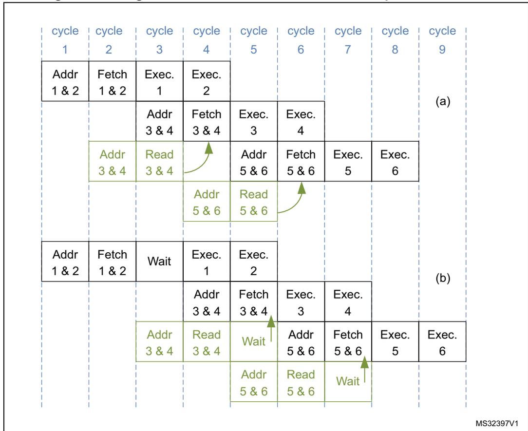
Figure 4 shows the timing to fetch a linear code in the NVM when the prefetch is disabled, both for 0 wait state (a) and 1 wait state (b). You can compare these two sequences with the ones in Figure 5, when the prefetch is enabled, to have an idea of the advantages of a prefetch on a linear code with 0 and 1 wait states.
Figure 4. Timing to fetch and execute instructions with prefetch disabled
| cycle 1 | cycle 2 | cycle 3 | cycle 4 | cycle 5 | cycle 6 | cycle 7 | cycle 8 | cycle 9 | cycle 10 | cycle 11 | |
|---|---|---|---|---|---|---|---|---|---|---|---|
| Addr 1 & 2 | Fetch 1 & 2 | Exec. 1 | Exec. 2 | ||||||||
| Addr 3 & 4 | Fetch 3 & 4 | Exec. 3 | Exec. 4 | (a) | |||||||
| Addr 5 & 6 | Fetch 5 & 6 | Exec. 5 | Exec. 6 | ||||||||
| Addr 1 & 2 | Fetch 1 & 2 | Wait | Exec. 1 | Exec. 2 | |||||||
| Addr 3 & 4 | Fetch 3 & 4 | Wait | Exec. 3 | Exec. 4 | (b) | ||||||
| Addr 5 & 6 | Fetch 5 & 6 | Wait | Exec. 5 | Exec. 6 |
MS32396V1
- (a) corresponds to 0 wait state.
- (b) corresponds to 1 wait state.
Figure 5 shows the timing to fetch and execute instructions from the NVM with 0 wait states (a) and 1 wait state (b) when the prefetch is enabled. The read executed by the prefetch appears in green.
Read as data and pre-read
A data read from the memory interface, corresponds to any read operation that is not a fetch. The master reads operation constants and parameters as data. All reads done by DMA (to copy from one address to another) are read as data. No check is done on the location of the data read (can be in every area of the NVM).
At reset, (DISAB_BUF = 0, PRFTEN = 0, PRE_READ = 0), the memory interface uses 2 buffers organized in one group to store the last two values read as data.
In some particular cases (for example when the DMA is reading a lot of consecutive words in the NVM), it can be useful to enable the pre-read (PRE_READ = 1 with DISAB_BUF = 0). The pre-read works exactly like the prefetch: it is a speculative reading at the last data address increased by 4 (one word). With this configuration, one buffer of data is moved to a new group to store the pre-read value, while the second buffer continues to store the last value read. For a prefetch, the pre-read value is copied in the last read value if the master requests it, or is lost if the master requests a different address.
The pre-read has a lower priority than a normal read or a prefetch operation: this means that it will be launched only when no other type of read is ongoing. Pay attention to the fact that a pre-read used in a wrong situation can be harmful: in a code where a data read is not done linearly, reducing the number of buffers (from 2 to 1) used for the last read value can increase the number of accesses to the NVM (and the time to read the value). Moreover, this can generate a delay on prefetch. An example of this situation is the code Dhrystone, whose results are shown in the corresponding section.
As for a prefetch operation, the user must select the right moment to enable and disable the pre-read.
Figure 5. Timing to fetch and execute instructions with prefetch enabled
The diagram illustrates the timing of instruction fetch and execution across 9 cycles for two different configurations.
(a) Continuous execution with prefetch:
- Cycle 1: Addr 1 & 2
- Cycle 2: Fetch 1 & 2
- Cycle 3: Exec. 1, Addr 3 & 4 (speculative read)
- Cycle 4: Exec. 2, Fetch 3 & 4
- Cycle 5: Exec. 3, Addr 5 & 6 (speculative read)
- Cycle 6: Exec. 4, Fetch 5 & 6
- Cycle 7: Exec. 5
- Cycle 8: Exec. 6
- Cycle 9: (empty)
(b) Execution with a wait state:
- Cycle 1: Addr 1 & 2
- Cycle 2: Fetch 1 & 2
- Cycle 3: Wait, Addr 3 & 4 (speculative read)
- Cycle 4: Exec. 1, Fetch 3 & 4
- Cycle 5: Exec. 2, Addr 5 & 6 (speculative read)
- Cycle 6: Exec. 3, Fetch 5 & 6
- Cycle 7: Exec. 4
- Cycle 8: Exec. 5
- Cycle 9: Exec. 6
Green arrows indicate speculative read actions: from Fetch 3 & 4 to Addr 3 & 4 in (a), from Fetch 5 & 6 to Addr 5 & 6 in (a), and from Fetch 3 & 4 to Addr 5 & 6 in (b).
MS32397V1
Table 15 is a summary of the possible configurations.
Table 15. Configurations for buffers and speculative reading
| DISAB_BUF | PRFTEN | PRE_READ | Description |
|---|---|---|---|
| 1 | X | X | Buffers disabled |
| 0 | 0 | 0 | Buffer enabled: no speculative reading is done |
| 0 | 1 | 0 | Prefetch enabled: speculative reading on fetch enabled |
| 0 | 0 | 1 | pre-read enabled: speculative reading on data enabled |
| 0 | 1 | 1 | Prefetch and pre-read enabled: speculative reading on fetch and data enabled |
Dhrystone performances
The Dhrystone test is used to evaluate the memory interface performances. The test has been executed in all memory interface configurations. Refer to Table 16 for a summary of the results.
Common parameters are:
- • the matrix size is 20 x 20
- • the loop is executed 1757 times
- • the version of Arm ® compiler is 4.1 [Build 561]
Here is some explanation about the results:
Table 16. Dhrystone performances in all memory interface configurations
| Number of wait states | DISAB_BUF | PRFTEN | PRE_READ | Number of DMIPS (x1000) | DMIPS x MHz |
|---|---|---|---|---|---|
| 0 | 1 | 0 | 0 | 953 | 15.25 |
| 0 | 0 | 0 | 0 | 953 | 15.25 |
| 0 | 0 | 1 | 0 | 953 | 15.25 |
| 0 | 0 | 0 | 1 | 953 | 15.25 |
| 0 | 0 | 1 | 1 | 953 | 15.25 |
| 1 | 1 | 0 | 0 | 677 | 21.66 |
| 1 | 0 | 0 | 0 | 690 | 22.08 |
| 1 | 0 | 1 | 0 | 823 | 26.34 |
| 1 | 0 | 0 | 1 | 691 | 22.11 |
| 1 | 0 | 1 | 1 | 816 | 26.11 |
- • The pre-read is not useful for this test: when enabled with the prefetch, it reduces the memory interface performance because only one buffer is used to store the last data read and, in this code, the master rarely reads the data linearly. This justifies the very small increase of performance when enabled without a prefetch.
- • The buffers (without speculative readings) with 1 wait state give a little advantage that can be considered without any costs.
- • At a 0 wait state, the best performance (as certified by Arm ® ) may be due to a different code alignment during the compilation.
3.3.4 Writing/erasing the NVM
There are many ways to change the NVM content. The memory interface helps to reduce the possibility of unwanted changes and to implement by hardware all sequences necessary to erase or write in the different memory areas.
Write/erase protocol
To write/erase memory content when the protections have been removed, the user needs to:
- 1. configure the operation to execute,
- 2. send to the memory interface the right number of data, writing one or several addresses in the NVM,
- 3. wait for the operation to complete.
During the waiting time, the user can prepare the next operation (except in very particular cases) writing the new configuration and starting to write data for the next write/erase operation.
The waiting time depends on the type of operation. A write/erase can last from \( T_{prog} \) (3.2 ms) to \( 2 \times T_{glob} \) (3.7 ms) + \( T_{prog} \) (3.2 ms). The memory interface can be configured to write a half-page (16 words in the Flash program memory) with only one waiting time. This can reduce the time to program a big amount of data.
Two different protocols can be used: single programming and multiple programming operation.
Single programming operation
With this protocol, the software has to write a value in a not-protected address of the NVM. When the memory interface receives this writing request, it stalls the master for some pulses of clock (for more details, see Table 17 ) while it checks the protections and the previous value and it latches the new value inside the NVM. The software can then start to configure the next operation. The operation will complete when the EOP bit of FLASH_SR register rises (if it was 0 at the operation start). The operation time is resumed in Table 19 for all operations.
Multiple programming operation (half page)
You can write a half-page (16 words) in Flash program memory. To execute this protocol, follow the next conditions:
- • PGAERR bit in the FLASH_SR register has to be zero (no previous alignment errors).
- • The first address has to be half-page aligned (the 6 lower bits of the address have to be at zero).
- • All 16 words must be in the same half-page (address bits 7 to 31 must be the same for all 16 words). This means that the first address sets the half-page and the next ones must be inside this half-page. The written data will be stored sequentially in the next addresses. It is not important that the addresses increase or change (for example, the same address can be used 16 times), as the memory interface will automatically increase the address internally.
- • Only words (32 bits) can be written.
When the memory interface receives the first address, it stalls the master for some pulses of clock while it checks the protections and the previous value and it latches the new value inside the NVM (for more details, see Table 17 ). Then, the memory interface waits for the second address. No read is accepted: only a fetch will be executed, but it aborts the ongoing write operation. After the second address, the memory interface stalls the core for a short time (less than the previous one) to perform a check and to latch it in the NVM before waiting for the next one. This sequence continues until all 16 words have been latched inside the NVM. A wrong alignment or size will abort the write operation. If the 16 addresses are correctly latched, the memory interface starts the write operation. The operation will complete when EOP bit of FLASH_SR register rises (if it was 0 at the operation start). The operation time is resumed in Table 19 .
This protocol can be used either through application code running from RAM or through DMA with application code running from RAM or core sleeping.
Unlocking/locking operations
Before performing a write/erase operation, it is necessary to enable it. The user can write into the Flash program memory, data EEPROM and Option bytes areas.
To perform a write/erase operation, unlock PELOCK bit of the FLASH_PECR register. When this bit is unlocked (its value is 0), the other bits of the same register can be modified. When PELOCK is 0, the write/erase operations can be executed in the data EEPROM.
To write/erase the Flash program memory, unlock PRGLOCK bit of the FLASH_PECR register. The bit can only be unlocked when PELOCK is 0.
To write/erase the user Option bytes, unlock OPTLOCK bit of the FLASH_PECR register. The bit can only be unlocked when PELOCK is 0. No relation exists between PRGLOCK and OPTLOCK: the first one can be unlocked when the second one is locked and vice versa.
Unlocking the data EEPROM and the FLASH_PECR register
After a reset, the data EEPROM and the FLASH_PECR register are not accessible in write mode because PELOCK bit in the FLASH_PECR register is set. The same unlocking sequence unprotects both of them at the same time.
The following sequence is used to unlock the data EEPROM and the FLASH_PECR register:
- • Write PEKEY1 = 0x89ABCDEF to the FLASH_PEKEYR register
- • Write PEKEY2 = 0x02030405 to the FLASH_PEKEYR register
For code example, refer to A.3.1: Unlocking the data EEPROM and FLASH_PECR register code example .
Any wrong key sequence will lock up FLASH_PECR until the next reset and generate a hard fault. Idem if the master tries to write another register between the two key sequences or if it uses the wrong key. A reading access does not generate an error and does not interrupt the sequence. A hard fault is returned in any of the four cases below:
- • After the first write access if the PEKEY1 value entered is erroneous.
- • During the second write access if PEKEY1 is correctly entered but the value of PEKEY2 does not match.
- • If there is any attempt to write a third value to PEKEYR (pay attention: this is also true for the debugger).
- • If there is any attempt to write a different register of the memory interface between PEKEY1 and PEKEY2.
When properly executed, the unlocking sequence clears PELOCK bit in the FLASH_PECR register.
To lock FLASH_PECR and the data EEPROM again, the software only needs to set PELOCK bit in FLASH_PECR. When locked again, PELOCK bit needs a new sequence to return to 0.
For code example, refer to A.3.2: Locking data EEPROM and FLASH_PECR register code example .
Unlocking the Flash program memory
An additional protection is implemented to write/erase the Flash program memory.
After a reset, the Flash program memory is no more accessible in write mode: PRGLOCK bit is set in the FLASH_PECR register. A write access to the Flash program memory is granted by clearing PRGLOCK bit.
The following sequence is used to unlock the Flash program memory:
- • Unlock the FLASH_PECR register (see the Unlocking the data EEPROM and the FLASH_PECR register section).
- • Write PRGKEY1 = 0x8C9DAEBF to the FLASH_PRGKEYR register.
- • Write PRGKEY2 = 0x13141516 to the FLASH_PRGKEYR register.
For code example, refer to A.3.3: Unlocking the NVM program memory code example .
If the keys are written with PELOCK set to 1, no error is generated and PRGLOCK remains at 1. It will be unlocked while re-executing the sequence with PELOCK = 0.
Any wrong key sequence will lock up PRGLOCK in FLASH_PECR until the next reset, and return a hard fault. A hard fault is returned in any of the four cases below:
- • After the first write access if the entered PRGKEY1 value is erroneous.
- • During the second write access if PRGKEY1 is correctly entered but the PRGKEY2 value does not match.
- • If there is any attempt to write a third value to PRGKEYR (this is also true for the debugger).
- • If there is any attempt to write a different register of the memory interface between PRGKEY1 and PRGKEY2.
When properly executed, the unlocking sequence clears the PRGLOCK bit and the Flash program memory is write-accessible.
To lock the Flash program memory again, the software only needs to set PRGLOCK bit in FLASH_PECR. When locked again, PRGLOCK bit needs a new sequence to return to 0. If PELOCK returns to 1 (locked), PRGLOCK is automatically locked, too.
Unlocking the Option bytes area
An additional write protection is implemented on the Option bytes area. It is necessary to unlock OPTLOCK to reload or write/erase the Option bytes area.
After a reset, the Option bytes area is not accessible in write mode: OPTLOCK bit in the FLASH_PECR register is set. A write access to the Option bytes area is granted by clearing OPTLOCK.
The following sequence is used to unlock the Option bytes area:
- 1. Unlock the FLASH_PECR register (see the Unlocking the data EEPROM and the FLASH_PECR register section).
- 2. Write OPTKEY1 = 0xFBЕAD9C8 to the FLASH_OPTKEYR register.
- 3. Write OPTKEY2 = 0x24252627 to the FLASH_OPTKEYR register.
For code example, refer to A.3.4: Unlocking the option bytes area code example .
If the keys are written with PELOCK = 1, no error is generated, OPTLOCK remains at 1 and it will be unlocked when re-executing the sequence with PELOCK to 0.
Any wrong key sequence will lock up OPTLOCK in FLASH_PECR until the next reset, and return a hard fault. A hard fault is returned in any of the four cases below:
- • After the first write access if the OPTKEY1 value entered is erroneous.
- • During the second write access if OPTKEY1 is correctly entered but the OPTKEY2 value does not match.
- • If there is any attempt to write a third value to OPTKEYR (this is also true for the debugger).
- • If there is any attempt to write a different register of the memory interface between OPTKEY1 and OPTKEY2.
When properly executed, the unlocking sequence clears the OPTLOCK bit and the Option bytes area is write-accessible.
To lock the Option bytes area again, the software only needs to set OPTLOCK bit in FLASH_PECR. When relocked, OPTLOCK bit needs a new sequence to return to 0. If PELOCK returns to 1 (locked), OPTLOCK is automatically locked, too.
Select between different types of operations
When the necessary unlock sequence has been executed (PELOCK, PRGLOCK and OPTLOCK), the user can enable different types of write and erase operations, writing the right configuration in the FLASH_PECR register. The bits involved are:
- • PRG
- • DATA
- • FIX
- • ERASE
- • FPRG
Detailed description of NVM write/erase operations
This section details the different types of write and erase operations, showing the necessary bits for each one.
Write to data EEPROM
- •
Purpose
Write one word in the data EEPROM with a specific value. - •
Size
Write by byte, half-word or word. - •
Address
Select a valid address in the data EEPROM. - •
Protocol
Single programming operation. - •
Requests
PELOCK = 0, ERASE = 0. - •
Errors
WRPERR is set to 1 (and the write operation is not executed) if PELOCK = 1 or if the memory is read-out protected. - •
Description
This operation aims at writing a word or a part of a word in the data EEPROM. The user must write the right value at the right address and with the right size. The memory interface automatically executes an erase operation when necessary (if all bits are currently set to 0, there is no need to delete the old content before writing). Similarly, if the data to write is at 0, only the erase operation is executed. When only a write operation or an erase operation is executed, the duration is T prog (3.2 ms); if both are executed, the duration is 2 x T prog (6.4 ms). It is possible to force the memory interface to execute every time both erase and write operations set the FIX flag to 1. - •
Duration
T prog (3.2 ms) or 2 x T prog (6.4 ms). - •
Options
Set the FIX bit to force the memory interface to execute every time an erase (to delete the old content) and a write operation (to write new data) occur. This gives a fix time for the operation for any data value and for previous data. - • Erase/write endurance cycles in data EEPROM are linked to one single word granularity (one erase/write cycle degrades only one programmed word area in data EEPROM).
For code example, refer to A.3.5: Write to data EEPROM code example .
Erase data EEPROM
- • Purpose
Delete one row in data EEPROM. This operation performs the same function as Write a word which size is null to data EEPROM. It is available for compatibility purpose only. - • Size
Erase only by word. - • Address
Select one valid address in the data EEPROM. - • Protocol
Single programming operation. - • Requests
PELOCK = 0, ERASE = 1 (optional DATA = 1). - • Errors
WRPERR is set to 1 if PELOCK = 1 or if the memory is read-out protected.
SIZERR is set to 1 if the size is not a word. - • Description
This operation aims at deleting the content of a row in the data EEPROM. A row contains only 1 word. The user must write a value at the right address with a word size. The data is not important: only an erase is executed (also with data different from zero). - • Duration
Tprog (3.2 ms).
For code example, refer to A.3.6: Erase to data EEPROM code example .
Write Option bytes
- • Purpose
Write one word in the Option bytes area with a specific value. - • Size
Write only by word. - • Address
Select a valid address in the Option bytes area. - • Protocol
Single programming operation. - • Requests
PELOCK = 0, OPTLOCK = 0, ERASE = 0. - • Errors
WRPERR is set to 1 if PELOCK = 1 or OPTLOCK = 1.
WRPERR is set to 1 if the actual read-out protection level is 2 (the Option bytes area cannot be written at Level 2).
SIZERR is set to 1 if the size is not the word - • Description
This operation aims at writing a word in the Option bytes area. The Option bytes area can only be written in Level 0 or Level 1.
The user must consider that, in a word, the 16 higher bits (from 16 to 31) have to be the complement of the 16 lower bits (from 0 to 15): a mismatch between the higher and lower parts of data would generate an error during the Option bytes loading (see Section 3.8: Option bytes ) and force the memory interface to load the default values. The memory interface does not check at the write time if the data is correctly complemented. The user must write the desired value at the right address with a word size.
As for data EEPROM, the memory interface deletes the previous content before writing, if necessary. If the data to write is at 0, the memory interface does not execute the useless write operation. When only a write operation or only an erase operation is executed, the duration is T prog (3.2 ms). If both are executed, the duration is 2 x T prog (6.4 ms). The memory interface can be forced to execute every time both erase and write operations set the FIX flag to 1.
Some configurations need a closer attention because they change the protections. The memory interface can change the Option bytes write in a Mass Erase or force some bits not to reduce the protections: for more details, see Section 3.4.4: Write/erase protection management .
- • Duration
T prog (3.2 ms) or 2 x T prog (6.4 ms). - • Options
FIX bit can be set to force the memory interface to execute every time an erase (to delete the old content) and a write operation (to write the new data) occur. This gives a fix time to program for every data value and for previous data.
For code example, refer to A.3.7: Program Option byte code example .
Erase Option bytes
- • Purpose
Delete one row in the Option bytes area. This operation performs the same function as Write Option Byte with a zero value. It is available for compatibility purpose only. - • Size
Erase only by word. - • Address
Select a valid address in the Option bytes area. - • Protocol
Single programming operation. - • Requests
PELOCK = 0, OPTLOCK = 0, ERASE = 1 (optional OPT = 1). - • Errors
WRPERR is set to 1 if PELOCK = 1 or OPTLOCK = 1.
WRPERR is set to 1 if the actual protection level is 2 (the Option bytes area cannot be erased at Level 2).
SIZERR is set to 1 if the size is not the word. - • Description
This operation aims at deleting the content of a row in the Option bytes area. A row contains only 1 word. The user must write zero at the right address with a word size.
Refer to Section : Write Option bytes for additional information.
Since all bits are set to 0 after an erase operation, there will be a mismatch during the Option bytes loading and the default values will be loaded. - • Duration
Tprog (3.2 ms).
For code example, refer to A.3.8: Erase Option byte code example .
Program a single word to Flash program memory
- • Purpose
Write one word in the Flash program memory with a specific value. - • Size
Write only by word. - • Address
Select an address in the Flash program memory. - • Protocol
Single programming operation. - • Requests
PELOCK = 0, PRGLOCK = 0. - • Errors
WRPERR is set to 1 if PELOCK = 1 or PRGLOCK = 1.
WRPERR is set to 1 if the user tries to write in a write-protected sector (see the PcROP (Proprietary Code Read-Out Protection) section).
NOTZEROERR is set to 1 if the user tries to write a value in a word which is not zero. This error does not stop the write operation on category 3 devices while the operation is stopped on other categories.
SIZERR is set to 1 if the size is not a word. - • Description
This operation allows writing a word in Flash program memory. The user must write the right value at the right address with a word size. The memory interface cannot execute an erase to delete the previous content before the write operation is performed.
If the previous content is not null:- – Category 3 devices
NOTZEROERR is set to 1.
The real value written in the memory is the OR of the previous value and the new value (the memory interface writes 1 when there was 0 before). This is done both for data and ECC. Reading back the data might not return the old value, the new one or the ORed values. The ECC is not compatible with the data any more. - – Other categories
NOTZEROERR is set to 1. Writing a word to an address containing a non-null value is not performed.
- – Category 3 devices
- • Duration
Tprog (3.2 ms). - • The erase/write endurance cycles in Flash program memory are linked to one page granularity (one erase/write cycle will degrade one programmed page in word area in Flash program memory).
For code example, refer to A.3.9: Program a single word to Flash program memory code example .
Program half-page in Flash program memory
- • Purpose
Write one half page (16 words) in the Flash program memory. - • Size
Write only by word. - • Address
Select one address in the Flash program memory aligned to a half-page (for the first address) and inside the same half-page selected by the second address for the next 15 addresses. - • Protocol
Multiple programming operation. - • Requests
PELOCK = 0, PRGLOCK = 0, FPRG = 1, PRG = 1. - • Errors
WRPERR is set to 1 if PELOCK = 1 or PRGLOCK = 1. WRPERR is set to 1 if the user tries to write in a write-protected sector (see the PcROP (Proprietary Code Read-Out Protection) section).
NOTZEROERR is set to 1 if the user tries to write a value in a word which is not zero. This error does not stop the write operation on category 3 devices while the operation is stopped on other categories. The check is done when all 16 addresses have been received, before the current write phase in Flash memory. The error flags are set only when all checks are performed.
SIZERR is set to 1 if the size is not the word.
PGAERR is set to 1 if the first address is not aligned to a half-page and if one of the following addresses (address from 2 to 16) is outside the half-page determined by the first address. No check is done to verify if the address has increased or if it has changed: this is done automatically by the memory interface. What is important is that the first address is aligned to the half-page, and that the next addresses are in the same half-page.
FWWERR is set to 1 if the write is aborted because the master fetched in the NVM. The read as data does not stop the write operation. - • Description
This operation allows writing a half-page in Flash program memory. The user must write the 16 desired values at the right address with a word size (as explained in the multiple programming operation). The memory interface cannot execute an erase to delete the previous content before writing (the user must delete the page before writing).
As for the single programming operation, if the previous content is not null:- – Category 3 devices
NOTZEROERR is set to 1.
The written value is the OR of previous and new data. This means that reading back the written address may return a value which is different from the written one.
- – Category 3 devices
- – Other categories
NOTZEROERR is set to 1. Writing a word to an address containing a non-null value is not performed.
When a half-page operation starts, the memory interface waits for 16 addresses/data, aborting (with a hard fault) all read accesses that are not a fetch (refer to Fetch and prefetch ). A fetch stops the half-page operation. The memory content remains unchanged, the FWWERR error is set in the FLASH_SR register. To complete the half-page programming operation, all the desired values should be written again.
- • Duration
Tprog (3.2 ms).
For code example, refer to A.3.10: Program half-page to Flash program memory code example .
Parallel write half-page Flash program memory
- • Purpose
Write 2 half-pages (one per bank) in parallel in Flash program memory.
- • Size
Write only by word.
- • Address
For each half-page, one address, aligned to half-page start address, must be selected in Flash program memory. The following 15 addresses must point to the half-page selected by first address.
Furthermore, the addresses of the second half-page must be on a different bank with respect to the start address of the first half-page (only the first address is checked).
- • Protocol
Multiple programming operation.
- • Requests
PELOCK = 0, PRGLOCK = 0, FPRG = 1, PRG = 1, PARALLELBANK=1.
- • Errors
This operation can generate the same kind of errors as program half-page in flash program memory. However, PGAERR is also generated when the second half-page selected is located in the same bank as the first half-page.
All the errors detected during this operation abort the whole program operation (i.e. both banks).
- • Description
This operation programs in parallel one half-page on both Flash program memory banks. This speeds up the initial programming of the whole NVM.
It is possible to start with Bank 1 or Bank 2.
- • Duration
Tprog (3.2 ms).
Erase a page in Flash program memory- •
Purpose
Delete one page (32 words) in the Flash program memory. - •
Size
Erase only by word (it deletes a page of the Flash program memory writing with a word size) - •
Address
Select a valid address in the Flash program memory. - •
Protocol
Single programming operation. - •
Requests
PELOCK = 0, PRGLOCK = 0, ERASE = 1, PRG = 1. - •
Errors
WRPERR is set to 1 if PELOCK = 1 or PRGLOCK = 1.
WRPERR is set to 1 if the row is in a protected sector (see PcROP (Proprietary Code Read-Out Protection) ).
SIZERR is set to 1 if the size is not the word. - •
Description
This operation aims at deleting the content of a row in the Flash program memory. The user must write a value in the right address with a word size. The data is not important: only an erase is executed (also with data not at zero). The address does not need to be aligned to the page: the memory interface will delete the page which contains the address. - •
Duration
Tprog (3.2 ms).
For code example, refer to A.3.11: Erase a page in Flash program memory code example .
Mass erase
- • Purpose
Remove the read and write protection on the Flash program memory and data EEPROM. - • Size
Erase only by word. - • Address
To generate a mass erase, it is necessary to write 0x015500AA to the first Option bytes address (bits 31 to 25 and 15 to 9 are not complemented because they are not used, and not checked) with Level 1 as the actual level. - • Protocol
Single programming operation. - • Requests
PELOCK = 0, OPTLOCK = 0, Protection Level = 1, the lower nibble of data has to be 0xAA (Level 0), with 0x55 as the third nibble. - • Errors
WRPERR is set to 1 if PELOCK = 1 or OPTLOCK = 1.
WRPERR is set to 1 if the actual protection level is 2 (the Option bytes area cannot be written in Level 2).
SIZERR is set to 1 if the size is not the word. - • Description
This operation is similar to the write user Option byte operation: the memory interface changes it in a mass erase when the actual Protection Level is 1 and the requested Protection Level is 0. The user must write the desired value in the first address of the Option bytes area with a word size.
A mass erase deletes the content of the Flash program memory and data EEPROM, changes the protection level to Level 0 and disables PcROP. (WPRMOD = 0). The bits write protection and BOR_LEVEL remain unchanged.
Unlike all other operations, the software cannot request new writing operations while a mass erase is ongoing. To be sure that a mass erase has completed, the software can reset the EOP bit of FLASH_SR register before the write operation and check when EOP goes to 1 (End Of Program). If this limitation is not respected, a wrong value may be written in the Flash program memory and data EEPROM when the Protection Level is written, thus adding unwanted protections (also for mismatch) that could make the device useless. - • Duration
2 x Tprog (6.4 ms) + Tglob (3.7 ms)
For code example, refer to A.3.12: Mass erase code example .
Timing tables
Table 17. NVM write/erase timings
| Operation | Delay to latch the first address/data (in AHB clock pulses) | Delay to latch the next address/data (in AHB clock pulses) |
|---|---|---|
| Write to data EEPROM | 18 | - |
| Erase data EEPROM | 17 | - |
| Write Option bytes | 18 | - |
| Erase Option bytes | 17 | - |
| Program a single word in Flash program memory | 78 | - |
| Program half-page in Flash program memory | 63 | 6 |
| Erase a page in Flash program memory | 76 | - |
Table 18. NVM write/erase duration
| Operation | Parameters/Conditions | Duration |
|---|---|---|
| Write to data EEPROM | Previous data = 0 FIX = 0 | Tprog (3.2 ms) |
| Previous data != 0 New data = 0 Size = word FIX = 0 | Tprog (3.2 ms) | |
| Other situations | 2 x Tprog (6.4 ms) | |
| Erase data EEPROM | - | Tprog (3.2 ms) |
| Write Option bytes | Previous data = 0 FIX = 0 | Tprog (3.2 ms) |
| Previous data != 0 New data = 0 FIX = 0 | Tprog (3.2 ms) | |
| Other situations | 2 x Tprog (6.4 ms) | |
| Erase Option bytes | - | Tprog (3.2 ms) |
| Program a single word in Flash program memory | - | Tprog (3.2 ms) |
| Program a half-page in Flash program memory | - | Tprog (3.2 ms) |
| Erase a page in Flash program memory | - | Tprog (3.2 ms) |
| Mass erase | - | 2 x Tprog (6.4 ms) + Tglob (3.7 ms) |
Status register
The FLASH_SR Status Register gives some information on the memory interface or the NVM status (operation(s) ongoing) and about errors that happened.
BSY
This flag is set and reset by hardware. It is set to 1 every time the memory interface executes a write/erase operation, and it informs that no other operation can be executed. If a new operation is requested, different behaviors can occur:
- • Waiting for read, or waiting for write/erase, or waiting for option loading:
If the software requests a write operation while a write/erase operation is executing (HVOFF = 0), the memory interface stalls the master and has the pending operation execute as soon as the write/erase operation is complete. - • Hard fault:
If the software requests a data read in a half-page operation when the memory interface is waiting for the next address/data (BSY is already 1 but HVOFF = 0), the memory interface generates a hard fault (because it cannot execute the read) and continues to wait for missing addresses. - • RDERR error:
If the software requests a read operation while a write/erase operation is executing (HVOFF = 0) but the address is protected, the memory interface rises the flag and continues to wait for the end of the write/erase operation. - • Write abort:
If the software fetches in the NVM when the memory interface is waiting for an address/data in a half-page operation, the write/erase operation is aborted, the FWWERR flag is raised and the fetch is executed.
EOP
This flag is set by hardware and reset by software. The software can reset it writing 1 in the status register. This bit is set when the write/erase operation is completed and the memory interface can work on other operations (or start to work on pending operations).
It is useful to clear it before starting a new write/erase operation, in order to know when the actual operation is complete. It is very important to wait for this flag to rise when a mass erase is ongoing, before requesting a new operation.
HVOFF
This flag is set and reset by hardware and it is a memory interface information copy coming from the NVM: it informs when the High-Voltage Regulators are on (= 0) or off (= 1).
PGAERR
This flag is set by hardware and reset by software. It informs when an alignment error happened. It is raised when:
- • The first address in a half-page operation is not aligned to a half-page (lower 6 bits equal to zero).
- • A half-page change happened in a half-page operation (the addresses from 2 to 16 in a half-page operation are not in the same half-page, selected by the first address).
An alignment error aborts the write/erase operation and an interrupt can be generated (if ERRRIE = 1 in the FLASH_PECR register). The content of the NVM is not changed.
If this flag is set, the memory interface blocks all other half-page operations.
To reset this flag, the software need to write it to 1.
SIZERERR
This flag is set by hardware and reset by software. It informs when a size error happened. It is raised when:
- • A write by byte and half-word occurs in the Flash program memory and Option bytes.
- • An erase (with bit ERASE = 1 in FLASH_PECR register) by byte or half-word occurs in all areas.
A size error aborts the write/erase operation and an interrupt can be generated (if ERRIE = 1 in the FLASH_PECR register). The content of the NVM is not changed.
To reset this flag, the software needs to write it to 1.
NOTZEROERR
This flag is set by hardware and reset by software. It indicates that the application software is attempting to write to one or more NVM addresses that contain a non-zero value.
Except for category 3 devices, the modify operation is always aborted when this condition is met. For category 3 devices, a not-zero error does not abort the write/erase operation but the value might be corrupted.
In a write by half-page, all 16 words are checked between the first address/value and the second one, and the flag is only set when all words are checked. If the flag is set, it means that at least one word has an actual value not at zero.
In a write by word, only the targeted word is checked and the flag is immediately set if the content is not zero.
An interrupt is generated if ERRIE = 1 in FLASH_PECR register. To reset this flag, the application software needs to program it to 1.
Note: Notification of a not-zero error condition (i.e. NOTZEROERR flag and the associated interrupt) can be disabled by the application software via the NZDISABLE bit in FLASH_PECR register. However, for all device except category 3 devices, the condition is still checked internally and modify operation is anyway blocked
3.4 Memory protection
The user can protect part of the NVM (Flash program memory, data EEPROM and Option bytes areas) from unwanted write and against code hacking (unwanted read).
The read protection is activated by setting the RDP option byte and then applying a system reset to reload the new RDP option byte.
Note: If the read protection is set while the debugger has been active (through SWD) after last POR (power-on reset), apply a POR (power-on reset) or wakeup from Standby mode instead of a system reset (the option bytes loading is not sufficient).
Three types of protections are implemented.
3.4.1 RDP (Read Out Protection)
This type of protection aims at protecting against unwanted read (hacking) of the NVM content. This protection is managed by RDPROT bitfield in the FLASH_OPTR register. The value is loaded from the Option bytes area during a boot and copied in the read-only register.
Three protection levels are defined:
- • Level 0: no protection
Level 0 is set when RDPROT is set to 0xAA. When this level is enabled, and if no other protection is enabled, read and write can be done in the Flash program memory, data EEPROM and Option bytes areas without restrictions. It is also possible to read and write the backup registers freely.
- • Level 1: memory read protection
Level 1 is set when RDPROT is set to any value except 0xAA and 0xCC, respectively used for Level 0 and Level 2. This is the default protection level after an Option bytes erase or when there is a mismatch in the RDPROT field.
Level 1 protects the Flash program memory and data EEPROM. When protection Level 1 is set through boot from RAM, bootloader or debugger, a power-down or a standby is required to execute the user code.
When this level is enabled:
- – No access to the Flash program memory and data EEPROM (read both for fetch and data and write) and no backup register reading is performed if the debug features (single-wire), or the device boot in the RAM, or the System memory is connected. If the user tries to read the Flash memory or data EEPROM, a hard fault is generated. No restriction is present on other areas: it is possible to read and write/erase the Option bytes area and to execute or read in the System Memory.
- – All operations are possible when the boot is done in the Flash program memory.
- – Writing the first Option byte with a value that changes the protection level to Level 0 (it is necessary that byte 0 is 0xAA and byte 2 is 0x55), a mass erase is generated. The mass erase deletes the Flash program memory and data EEPROM, deletes the first Option byte and then rewrites it to enable Level 0 and disable PCROP (WPRMOD = 0), and deletes the backup registers content.
- • Level 2: disable debug and chip read protection
Level 2 is set when RDPROT is set to 0xCC. When this level is enabled, it is only possible to boot from the Flash program memory, and the debug features (single-wire) are disabled. The Option bytes are protected against write/erase and the protection level can no longer be changed. The application can write/erase to the Flash program memory and data EEPROM (it is only possible to boot from the Flash program memory and execute the customer code) and access the backup registers. When an Option bytes loading is executed and Level 2 is enabled, old information on debug or boot in the RAM or System memory are deleted.
Note: The debug feature is also disabled under reset. STMicroelectronics is not able to perform analysis on defective parts on which level 2 protection has been set.
Figure 6 resumes the way the protection level can be changed and Table 19 the link between the values read in the Option bytes and the protection level.
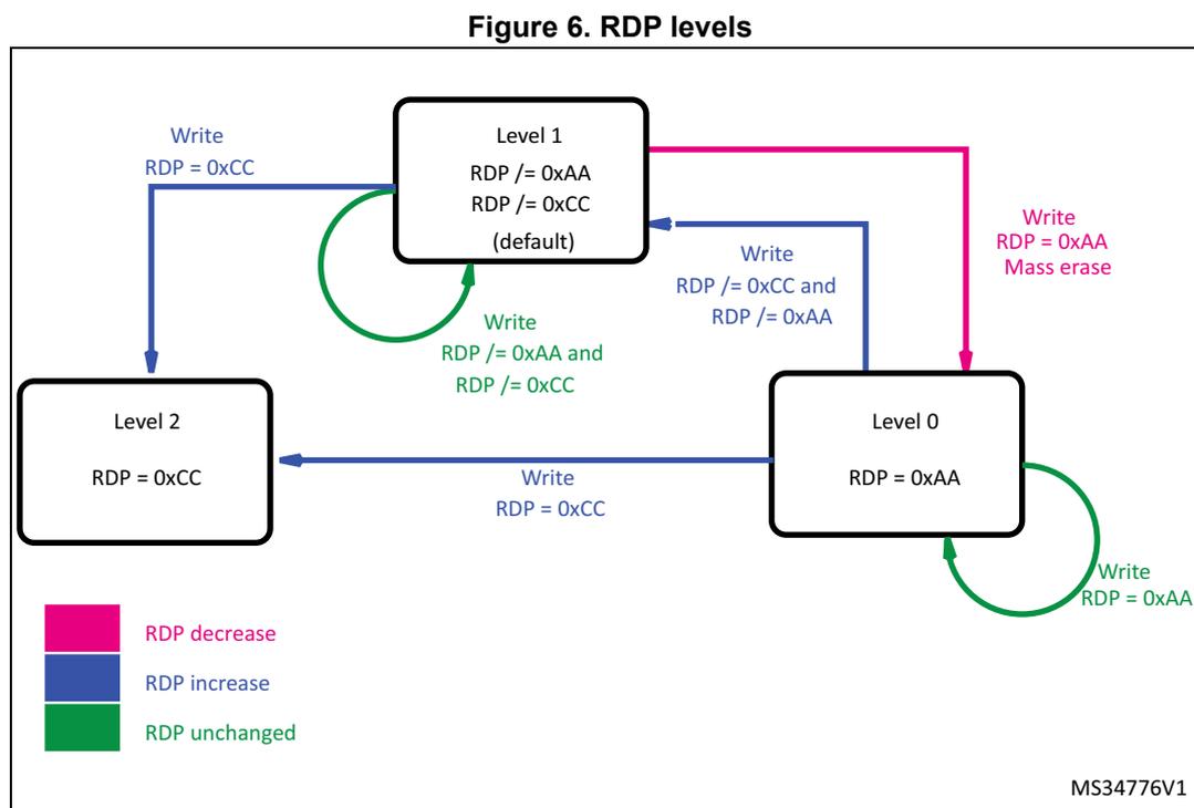
Figure 6. RDP levels
| RDP byte value | RDP complementary value | Read Protection status |
|---|---|---|
| 0xAA | 0x55 | Level 0 |
| 0xCC | 0x33 | Level 2 |
| Any other value | Complement of RDP byte | Level 1 |
| Any value | Not the complement value of RDP byte | Level 1 |
3.4.2 PcROP (Proprietary Code Read-Out Protection)
The Flash program memory can be protected from being read by a hacking code: the read data are blocked (not for a fetch). The protected code must not access data in the protected zone, including the literal pool.
The Flash program memory can be protected against a hacking code read: this blocks the data read (not for a fetch), assuming that the native code is compiled according to the PcROP option. This mode is activated setting WPRMOD = 1 in the FLASH_OPTR register.
The protection granularity is the sector (1 sector = 32 pages = 4 KB). To protect a sector, set to 0 the right bit in the WRPROT configuration: 0 means read and write protection, 1 means no protection.
Table 20 shows the link between the bits of the WRPROT configuration and the address of the Flash memory sectors.
Any read access performed as data (see Read as data and pre-read ) in a protected sector will trigger the RDERR flag in the FLASH_SR register. Any read-protected sector is also write-protected and any write access to one of these sectors will trigger the WRPERR flag in the FLASH_SR register.
Table 20. Link between protection bits of FLASH_WRPROTx register and protected address in Flash program memory
| Bit | Start address | End address | Bit | Start address | End address |
|---|---|---|---|---|---|
| 0 | 0x0800 0000 | 0x0800 0FFF | 24 | 0x0801 8000 | 0x0801 8FFF |
| 1 | 0x0800 1000 | 0x0800 1FFF | 25 | 0x0801 9000 | 0x0801 9FFF |
| 2 | 0x0800 2000 | 0x0800 2FFF | 26 | 0x0801 A000 | 0x0801 AFFF |
| 3 | 0x0800 3000 | 0x0800 3FFF | 27 | 0x0801 B000 | 0x0801 BFFF |
| 4 | 0x0800 4000 | 0x0800 4FFF | 28 | 0x0801 C000 | 0x0801 CFFF |
| 5 | 0x0800 5000 | 0x0800 5FFF | 29 | 0x0801 D000 | 0x0801 DFFF |
| 6 | 0x0800 6000 | 0x0800 6FFF | 30 | 0x0801 E000 | 0x0801 EFFF |
| 7 | 0x0800 7000 | 0x0800 7FFF | 31 | 0x0801 F000 | 0x0801 FFFF |
| 8 | 0x0800 8000 | 0x0800 8FFF | 32 | 0x0802 0000 | 0x0802 0FFF |
| 9 | 0x0800 9000 | 0x0800 9FFF | 33 | 0x0802 1000 | 0x0802 1FFF |
| 10 | 0x0800 A000 | 0x0800 AFFF | 34 | 0x0802 2000 | 0x0802 2FFF |
| 11 | 0x0800 B000 | 0x0800 BFFF | 35 | 0x0802 3000 | 0x0802 3FFF |
| 12 | 0x0800 C000 | 0x0800 CFFF | 36 | 0x0802 4000 | 0x0802 4FFF |
| 13 | 0x0800 D000 | 0x0800 DFFF | 37 | 0x0802 5000 | 0x0802 5FFF |
| 14 | 0x0800 E000 | 0x0800 EFFF | 38 | 0x0802 6000 | 0x0802 6FFF |
| 15 | 0x0800 F000 | 0x0800 FFFF | 39 | 0x0802 7000 | 0x0802 7FFF |
| 16 | 0x0801 0000 | 0x0801 0FFF | 40 | 0x0802 8000 | 0x0802 8FFF |
| 17 | 0x0801 1000 | 0x0801 1FFF | 41 | 0x0802 9000 | 0x0802 9FFF |
| 18 | 0x0801 2000 | 0x0801 2FFF | 42 | 0x0802 A000 | 0x0802 AFFF |
| 19 | 0x0801 3000 | 0x0801 3FFF | 43 | 0x0802 B000 | 0x0802 BFFF |
| 20 | 0x0801 4000 | 0x0801 4FFF | 44 | 0x0802 C000 | 0x0802 CFFF |
| 21 | 0x0801 5000 | 0x0801 5FFF | 45 | 0x0802 D000 | 0x0802 DFFF |
| 22 | 0x0801 6000 | 0x0801 6FFF | 46 | 0x0802 E000 | 0x0802 EFFF |
| 23 | 0x0801 7000 | 0x0801 7FFF | 47 | 0x0802 F000 | 0x0802 FFFF |
When WPRMOD = 1 (PcROP enabled), it is not possible to reduce the protection on a sector: new zeros (to protect new sectors) can be set, but new ones (to remove the protection from sectors) cannot be added. This is valid regardless of the protection level (RDPROT configuration). When WPRMOD is active, if the user tries to reset WPRMOD or to remove the protection from a sector, the programming is launched but WPRMOD or protected sectors remain unchanged.
The only way to remove a protection from a sector is to request a mass erase (which changes the protection level to 0 and disables PcROP): when PcROP is disabled, the protection on sectors can be changed freely.
3.4.3 Protections against unwanted write/erase operations
The memory interface implements two ways to protect against unwanted write/erase operations which are valid for all matrix or only for specific sectors of the Flash program memory.
As explained in the Unlocking/locking operations section, the user can:
- • Write/erase to the data EEPROM only when PELOCK = 0 in the FLASH_PECR register.
- • Write/erase to the Option bytes area only when PELOCK = 0 and OPTLOCK = 0 in the FLASH_PECR register.
- • Write/erase to the Flash program memory only when PELOCK = 0 and PRGLOCK = 0 in the FLASH_PECR register.
To see the sequences to set PELOCK, PRGLOCK and OPTLOCK, refer to the Unlocking the data EEPROM and the FLASH_PECR register , Unlocking the Flash program memory and Unlocking the Option bytes area sections.
In the Flash program memory, it is possible to add another write protection with the sector granularity. When PcROP is disabled (WPRMODE = 0), the bits of WRPROT are used to enable the write protection on the sectors. The polarity is opposed relatively to PcROP: to protect a sector, it is necessary to set the bit to 1; to remove the protection, it is necessary to set the bit to 0. Table 20 is valid for a write protection as well. As explained, when PcROP is enabled, the sectors protected against read are also protected against write/erase. It is always possible to change the write protection on sectors both in Level 0 and Level 1 (provided that it is possible to write/erase to Option bytes and that PcROP is disabled).
Table 21 resumes the protections.
Table 21. Memory access vs mode, protection and Flash program memory sectors
| Flash program memory sectors | Mode | ||||
|---|---|---|---|---|---|
| User (including In Application Programming) no Debug, or no Boot in RAM, or no Boot in System memory | User in Debug, or with Boot in RAM, or with Boot in System memory | ||||
| RDP | Level 1 Level 0 | Level 2 | Level 0 | Level 1 | Level 2 |
| Flash program memory (FLASH_PRGLOCK = 1) | R | R | R | Protected (no access) | NA (1) |
| Flash memory (FLASH_PRLOCK = 0) | R / W | R / W | R / W | Protected (no access) | NA (1) |
| Flash program memory in WRP pages | R | R | R | Protected (no access) | NA (1) |
Table 21. Memory access vs mode, protection and Flash program memory sectors (continued)
| Flash program memory sectors | Mode | ||||
|---|---|---|---|---|---|
| User (including In Application Programming) no Debug, or no Boot in RAM, or no Boot in System memory | User in Debug, or with Boot in RAM, or with Boot in System memory | ||||
| RDP | Level 1 Level 0 | Level 2 | Level 0 | Level 1 | Level 2 |
| Flash program memory in PCROP pages | Fetch | Fetch | Fetch | Protected (no access) | NA (1) |
| Data EEPROM (FLASH_PELOCK = 1) | R | R | R | Protected (no access) | NA (1) |
| Data EEPROM (FLASH_PELOCK = 0) | R / W | R / W | R / W | Protected (no access) | NA (1) |
| Option bytes (FLASH_OPTLOCK = 1) | R | R | R | R | NA (1) |
| Option bytes (FLASH_OPTLOCK = 0) | R / W | R | R / W | R / W | NA (1) |
1. NA stands for “not applicable”.
3.4.4 Write/erase protection management
Here is a summary of the rules to change all previous protections:
- • When the protection Level is 2, no protection change can be done.
- • When in Level 0 or 1, it is always possible to move to Level 2, writing xx33xxCC (the x are the hexadecimal digits that can have any value) in the first Option byte word.
- • When in Level 0, it is possible to move to Level 1, writing any value in the first Option byte word that is not xx33xxCC (Level 2) or xx55xxAA (Level 0).
- • when in Level 1, the protection can be reduced to Level 0, writing xx55xxAA in the first Option byte word. This generates a mass erase and deletes the PcROP field too.
- • It is always possible to enable PcROP (except in Level 2), writing x0xx1xx in the first Option byte word. If there is a mismatch during an Option byte loading on this flag, PcROP is enabled.
- • PcROP can be removed on requesting a mass erase (move from Level 1 to Level 0).
- • When PcROP is disabled, a write protection can be added on sectors (writing 1) or removed (writing 0) in the third word of the Option bytes. A mismatch concerns all write-protected sectors (if PcROP is disabled).
- • When PcROP is enabled, protected sectors can be added (writing 0) but cannot be removed. A mismatch concerns all read- and write-protected sectors (if PcROP is enabled).
- • A mass erase does not delete the third word of the Option bytes: the user must write it correctly.
3.4.5 Protection errors
Write protection error flag (WRPERR)
If an erase/program operation to a write-protected page of the Flash program memory and data EEPROM is launched, the Write Protection Error flag (WRPERR) is set in the FLASH_SR register. Consequently, the WRPERR flag is set when the software tries to:
- • Write to a WRP page.
- • Write to a System memory page or to factory option bytes.
- • Write to the Flash program memory, data EEPROM or Option bytes if they are not unlocked by PEKEY, PRGKEY or OPTKEY.
- • Write to the Flash program memory, data EEPROM or Option bytes when the RDP Option byte is set and the device is in debug mode or is booting from the RAM or from the System memory.
A write-protection error aborts the write/erase operation and an interrupt can be generated (if ERRIE = 1 in the FLASH_PECR register).
To reset this flag, the software needs to write it to 1.
Read error (RDERR)
If the software tries to read a sector protected by PcROP, the RDERR flag of FLASH_SR is raised. The data received on the bus is at 0.
If the error interrupt is enabled (ERRIE = 1 in the FLASH_PECR register), an interrupt is generated.
To reset this flag, the software needs to write it to 1.
3.5 NVM interrupts
Setting the End of programming interrupt enable bit (EOPIE) in the FLASH_PECR register enables an interrupt generation when an erase or a programming operation ends successfully. In this case, the End of programming (EOP) bit in the FLASH_SR register is set. To reset it, the software needs to write it to 1.
Setting the Error interrupt enable bit (ERRIE) in the FLASH_PECR register enables an interrupt generation if an error occurs during a programming or an erase operation request. In this case, one or several error flags are set in the FLASH_SR register:
- • RDERR (PCROP Read protection error flags)
- • WRPERR (Write protection error flags)
- • PGAERR (Programming alignment error flag)
- • OPTVERR (Option validity error flag)
- • SIZERR (Size error flag)
- • FWWERR (Fetch while write error flag)
- • NOTZEROERR (Write a not zero word error flag)
To reset the error flag, the software needs to write the right flag to 1.
Table 22. Flash interrupt request
| Interrupt event | Event flag | Enable control bit |
|---|---|---|
| End of operation | EOP | EOPIE |
| Error | RDERR WRPERR PGAERR OPTVERR SIZERR FWWERR NOTZEROERR | ERRIE |
3.5.1 Hard fault
A hard fault is generated on:
- • The memory bus if a read access is attempted when RDP is set.
- • The memory bus if a read as data is received; then, the memory interface is waiting for a data/address during a half-page write (after the 1 st address and before the 16 th address).
- • The register bus if an incorrect value is written in PEKEYR, PRGKEYR, or OPTKEYR.
3.6 Memory interface management
The purpose of this section is to clarify what happens when one operation is requested while another is ongoing: the way the different operations work together and are managed by the memory interface.
3.6.1 Operation priority and evolution
There are three types of operations and each of them has different flows:
Read
- • If no operation is ongoing and the read address is not protected, the read is executed without delays and with the actual configurations.
- • If the read address is protected, the operation is filtered (the read requested is never sent to the memory) and an error is raised.
- • If the read address is not protected but the memory interface is busy and cannot perform the operation, the read is put on hold to be executed as soon as possible.
Write/erase
- • If no operation is ongoing and the write address is not protected, the write/erase will start immediately; after some clock pulses (see Table 17 ) during which the bus and the
master are blocked, the memory interface continues the operation freeing the bus and the master.
- • If the address is protected, the write/erase is filtered (the write/erase requested is never sent to the memory) and an error is raised.
- • If the address is not protected but one or several conditions are not met, the operation is aborted (the abort needs more time to be executed because the NVM and data EEPROM need to return to default configuration) and an error is raised.
- • If the address to write/erase is not protected and all rules are respected, and if the memory interface is busy, the operation is put on hold to be executed as soon as possible.
Option byte loading
- • If a write/erase is ongoing, the Option byte loading waits for the end of operation then it is executed: no other write/erase is accepted, even if waiting.
- • If no write/erase is ongoing, the Option byte is executed directly (the read operation is executed until the system reset goes to 0 as a result of the Option byte request).
This means that the Option byte loading has a bigger priority than the read and write/erase operations. All other operations are executed in the order of request.
3.6.2 Sequence of operations
Read as data while write
If the master requests a read as data (see Read as data and pre-read ) while a write operation is ongoing, there are three different cases:
- 1. If the read is in a protected area, the RDERR flag is raised and the write operation continues.
- 2. If the write operation uses a Single programming operation or a Multiple programming operation (half page) and all addresses/data have been sent to the memory interface, any read operation from the same bank is put on hold and will be executed when the write operation is complete. It is important to emphasize that, during all the time spent when the read waits to be executed, the master is blocked and no other operation can be executed until the write and read operations are complete. However, any authorized read operation from the other bank is accepted and served.
- 3. if the write operation uses a Multiple programming operation (half page) and not all addresses/data have been sent to the memory interface, the read operation is not accepted whatever the targeted bank, a hard fault is generated and the memory interface continues to wait for the missing addresses/data to complete the write operation.
Fetch while write
If the master fetches an instruction while a write is ongoing, the situation is similar to a read as data (see step 1 and 2 above), but the last case is as follows:
- • If the write operation uses a Multiple programming operation (half page) and not all addresses/data have been sent to the memory interface, the write is aborted and it is as it had never happened: the read operation is accepted whatever the targeted bank, and the value is sent to the master.
Write while another write operation is ongoing
If the master requests a write operation while another one is ongoing, there are different cases:
- • If the previous write uses a Single programming operation or a Multiple programming operation (half page) and all addresses/data have been sent to the memory interface, and if the new write is in a protected area, the WRPERR flag is raised, the previous write continues and the new write is deleted.
- • If the previous write uses a Single programming operation or a Multiple programming operation (half page) and all addresses/data have been sent to the memory interface, and if the new Single programming operation or Multiple programming operation (half page) is not in a protected area, the new write is put on hold and will be executed when the first write operation is complete. It is important to emphasize that the master who requested the second write is blocked until the first write completes and the second has stored the address and data internally.
- • It is forbidden to request a new write when a mass erase is ongoing: during all the steps of the mass erase, the data is not stored internally and the new data can change the value stored as a protection, adding unwanted protections.
- • It is possible to change configurations to prepare a new write operation when the first operation uses a Single programming operation or a Multiple programming operation (half page) and all addresses/data have been sent to the memory interface.
3.6.3 Change the number of wait states while reading
To change the number of wait states, it is necessary to write to the FLASH_ACR register. The read/write of a register uses a different interface than the memory read/write. The number of wait states cannot be changed while the memory interface is reading and the memory interface cannot be stopped if a request is sent to the register interface. For this reason, while a master is reading the memory and another master changes the wait state number, the register interface will be locked until the change takes effect (until the readings stop). To stop the master which is changing the number of wait states, it is important to read back the content of the FLASH_ACR register: it is not possible to know the number of clock cycles that will be necessary to change the number of wait states as it depends on the customer code.
3.6.4 Power-down
To put the NVM in power-down, it is necessary to execute an unlocking sequence.
The following sequence is used to unlock RUN_PD bit of the FLASH_ACR register:
- • Write PDKEY1 = 0x04152637 to the FLASH_PDKEYR register.
- • Write PEKEY2 = 0xFAFBFCFD to the FLASH_PDKEYR register.
It is necessary to write the two keys without constraints about other read or write. No error is generated if the wrong key is used: when both have been written, RUN_PD bit is unlocked and can be written to 1, putting the NVM in power-down mode.
Resetting the RUN_PD flag to 0 (making the NVM available) automatically resets the sequence and the two keys are requested to re-enable RUN_PD.
3.7 Flash register description
Read registers
To read all internal registers of the memory interface, the user must read at the register addresses. The content is available immediately (no wait state is necessary to read registers). If the user tries to read the FLASH_ACR register after modifying the number of wait states, the content will be available when the change takes effect (when no read is done in the NVM memory, so the number of wait states is changed).
When no register is selected or when a wrong address is sent to the memory interface, a zero value is sent as an answer. No error is generated.
When the master sends a request to read 8 or 16 bits, the memory interface returns the corresponding part of the register on the data output bus. For example, if a register content is 0x12345678 and the master sends a request to read the second byte, the output will be 0x34343434 (because 0x34 is the content of the second register byte when starting to count bytes from zero). Similarly, if the master sends a request to read half-word zero of the previous register, the output will be 0x56785678.
Write to registers
In the configuration registers of the memory interface, there are two types of bits:
- • the bits that can be written to directly
- • the bits needing a particular sequence to unlock.
To know which category a bit belongs to, see the next sections where every bit is explained in details.
When it is possible to write directly to a register or a key-register, the user must write the expected value at the register address. If the address is not correct, no error is generated. If the user tries to modify a read-only register, no error is generated and the modify operation does not take any effect. It is possible to write registers by byte, half-word and word.
When an unlock sequence is necessary, the correct values to use are given.
3.7.1 Access control register (FLASH_ACR)
Address offset: 0x00
Reset value: 0x0000 0000
| 31 | 30 | 29 | 28 | 27 | 26 | 25 | 24 | 23 | 22 | 21 | 20 | 19 | 18 | 17 | 16 |
|---|---|---|---|---|---|---|---|---|---|---|---|---|---|---|---|
| Res. | Res. | Res. | Res. | Res. | Res. | Res. | Res. | Res. | Res. | Res. | Res. | Res. | Res. | Res. | Res. |
| 15 | 14 | 13 | 12 | 11 | 10 | 9 | 8 | 7 | 6 | 5 | 4 | 3 | 2 | 1 | 0 |
| Res. | Res. | Res. | Res. | Res. | Res. | Res. | Res. | Res. | PRE_READ | DISAB_BUF | RUN_PD | SLEEP_PD | Res. | PRFTEN | LATENCY |
| r/w | r/w | r/w | r/w | r/w | r/w |
Bits 31:7 Reserved, must be kept at reset value
Bit 6 PRE_READ
This bit enables the pre-read.
0: The pre-read is disabled
1: The pre-read is enabled. The memory interface stores the last address read as data and tries to read the next one when no other read or write or prefetch operation is ongoing.
Note: It is automatically reset every time the DISAB_BUF bit (in this register) is set to 1.
Bit 5 DISAB_BUF
This bit disables the buffers used as a cache during a read. This means that every read will access the NVM even for an address already read (for example, the previous address). When this bit is reset, the PRFTEN and PRE_READ bits are automatically reset, too.
0: The buffers are enabled
1: The buffers are disabled. Every time one NVM value is necessary, one new memory read sequence has to be done.
Bit 4 RUN_PD
This bit determines if the NVM is in power-down mode or in idle mode when the device is in run mode. It is possible to write this bit only when there is an unlocked writing of the FLASH_PDKEYR register.
The correct sequence is explained in Section 3.6.4: Power-down . When writing this bit to 0, the keys are automatically lost and a new unlock sequence is necessary to re-write it to 1.
0: When the device is in Run mode, the NVM is in Idle mode.
1: When the device is in Run mode, the NVM is in power-down mode.
Bit 3 SLEEP_PD
This bit allows to have the Flash program memory and data EEPROM in power-down mode or in idle mode when the device is in Sleep mode.
0: When the device is in Sleep mode, the NVM is in Idle mode.
1: When the device is in Sleep mode, the NVM is in power-down mode.
Bit 2 Reserved, must be kept at reset value
Bit 1 PRFTEN
This bit enables the prefetch. It is automatically reset every time the DISAB_BUF bit (in this register) is set to 1. To know how the prefetch works, see the Fetch and prefetch section.
- 0: The prefetch is disabled.
- 1: The prefetch is enabled. The memory interface stores the last address fetched and tries to read the next one when no other read or write operation is ongoing.
Bit 0 LATENCY
The value of this bit specifies if a 0 or 1 wait-state is necessary to read the NVM. The user must write the correct value relative to the core frequency and the operation mode (power). The correct value to use can be found in Table 13 . No check is done to verify if the configuration is correct.
To increase the clock frequency, the user has to change this bit to '1', then to increase the frequency. To reduce the clock frequency, the user has to decrease the frequency, then to change this bit to '0'.
- 0: Zero wait state is used to read a word in the NVM.
- 1: One wait state is used to read a word in the NVM.
3.7.2 Program and erase control register (FLASH_PECR)
Address offset: 0x04
Reset value: 0x0000 0007
This register can only be written after a good write sequence done in FLASH_PEKEYR, resetting the PELOCK bit.
| 31 | 30 | 29 | 28 | 27 | 26 | 25 | 24 | 23 | 22 | 21 | 20 | 19 | 18 | 17 | 16 |
|---|---|---|---|---|---|---|---|---|---|---|---|---|---|---|---|
| Res. | Res. | Res. | Res. | Res. | Res. | Res. | Res. | NZDISABLE | Res. | Res. | Res. | Res. | OBL_LAUNCH | ERRIE | EOPIE |
| rw | rw | rw | rw | ||||||||||||
| 15 | 14 | 13 | 12 | 11 | 10 | 9 | 8 | 7 | 6 | 5 | 4 | 3 | 2 | 1 | 0 |
| PARALLELBANK | Res. | Res. | Res. | Res. | FPRG | ERASE | FIX | Res. | Res. | Res. | DATA | PROG | OPT_LOCK | PRG_LOCK | PE_LOCK |
| rw | rw | rw | rw | rw | rw | rs | rs | rs |
Bits 31:24 Reserved, must be kept at reset value
Bit 23 NZDISABLE : Non-Zero check notification disable
When this bit is set, the application software does not check if the previous NVM content is zero before programming a word or an half-page in the program or boot area. As a result, the NOTZEROERR flag will always remain at 0 and no interrupt will be generated if the above condition is met. By default, NZDISABLE is set to 0. It can be modified only when PELOCK is 0.
0: error interrupt disabled
1: error interrupt enabled
On category 3 devices, this bit is not available and the behavior corresponds to NZDISABLE=0.
Bits 22:19 Reserved, must be kept at reset value
Bit 18 OBL_LAUNCH
Setting this bit, the software requests the reloading of Option byte. The Option byte reloading does not stop an ongoing modify operation, but it blocks new ones. The Option byte reloading generates a system reset.
0: Option byte loading completed.
1: Option byte loading to be done.
Note: This bit can only be modified when OPTLOCK is 0. Locking OPTLOCK (or other lock bits) does not reset this bit.
Bit 17 ERRIE : Error interrupt enable
0: Error interrupt disable.
1: Error interrupt enable.
Note: This bit can only be modified when PELOCK is 0. Locking PELOCK does not reset this bit; the interrupt remains enabled.
Bit 16 EOPIE : End of programming interrupt enable
0: End of program interrupt disable.
1: End of program interrupt enable.
Note: This bit can only be modified when PELOCK is 0. Locking PELOCK does not reset this bit; the interrupt remains enabled.
Bit 15 PARALLELBANK : Parallel bank programming mode.
This bit can be set and cleared by software when no program or erase operation is ongoing. When it is set, 2 half-pages can be programmed, the first one in Bank 1 and the second one in Bank 2.
0: Parallel bank mode disabled
1: Parallel bank mode enabled
This bit is available only for category 5 devices.
Bits 14:11 Reserved, must be kept at reset value
Bit 10 FPRG : Half Page programming mode
0: Half Page programming disabled.
1: Half Page programming enabled.
Note: This bit can be modified when PELOCK is 0. It is reset when PELOCK is set.
Bit 9 ERASE
0: No erase operation requested.
1: Erase operation requested.
Note: This bit can be modified when PELOCK is 0. It is reset when PELOCK is set.
Bit 8 FIX0: An erase phase is automatically performed, when necessary, before a program operation in the data EEPROM and the Option bytes areas. The programming time can be: \( T_{prog} \) (program operation) or \( 2 * T_{prog} \) (erase + program operations).
1: The program operation is always performed with a preliminary erase and the programming time is: \( 2 * T_{prog} \) .
Note: This bit can be modified when PELOCK is 0. It is reset when PELOCK is set.
Bits 7:5 Reserved, must be kept at reset value
Bit 4 DATA0: Data EEPROM not selected.
1: Data memory selected.
Note: This bit can be modified when PELOCK is 0. It is reset when PELOCK is set. This bit is not very useful as the page and word have the same size in the data EEPROM, but it is used to identify an erase operation (by page) from a word operation.
Bit 3 PROGThis bit is used for half-page program operations and for page erase operations in the Flash program memory.
0: The Flash program memory is not selected.
1: The Flash program memory is selected.
Note: This bit can be modified when PELOCK is 0. It is reset when PELOCK is set.
Bit 2 OPTLOCK: Option bytes lockThis bit blocks the write/erase operations to the user Option bytes area and the OBL_LAUNCH bit (in this register). It can only be written to 1 to re-lock. To reset to 0, a correct sequence of unlock with OPTKEYR register is necessary (see Unlocking the Option bytes area ), with PELOCK bit at 0. If the sequence is not correct, the bit will be locked until the next system reset and a hard fault is generated. If the sequence is executed when PELOCK = 1, the bit remains locked and no hard fault is generated. The keys to unlock are:
- – First key: 0xFBEAD9C8
- – Second key: 0x24252627
- 0: The write and erase operations in the Option bytes area are disabled.
1: The write and erase operations in the Option bytes area are enabled.
Note: This bit is set when PELOCK is set.
Bit 1 PRGLOCK: Program memory lockThis bit blocks the write/erase operations to the Flash program memory. It can only be written to 1 to re-lock. To reset to 0, a correct sequence of unlock with PRGKEYR register is necessary (see Unlocking the Flash program memory ), with PELOCK bit at 0. If the sequence is not correct, the bit will be locked until the next system reset and a hard fault is generated. If the sequence is executed when PELOCK = 1, the bit remains locked and no hard fault is generated. The keys to unlock are:
- – First key: 0x8C9DAEBF
- – Second key: 0x13141516
- 0: The write and erase operations in the Flash program memory are disabled.
1: The write and erase operations in the Flash program memory are enabled.
Note: This bit is set when PELOCK is set.
Bit 0 PELOCK: FLASH_PECR lockThis bit locks the FLASH_PECR register. It can only be written to 1 to re-lock. To reset to 0, a correct sequence of unlock with PEKEYR register (see Unlocking the data EEPROM and the FLASH_PECR register ) is necessary. If the sequence is not correct, the bit will be locked until the next system reset and one hard fault is generated. The keys to unlock are:
- – First key: 0x89ABCDEF
- – Second key: 0x02030405
- 0: The FLASH_PECR register is unlocked; it can be modified and the other bits unlocked.
Data write/erase operations are enabled.
1: The FLASH_PECR register is locked and no write/erase operation can start.
3.7.3 Power-down key register (FLASH_PDKEYR)
Address offset: 0x08
Reset value: 0x0000 0000
| 31 | 30 | 29 | 28 | 27 | 26 | 25 | 24 | 23 | 22 | 21 | 20 | 19 | 18 | 17 | 16 |
| FLASH_PDKEYR[31:16] | |||||||||||||||
| w | w | w | w | w | w | w | w | w | w | w | w | w | w | w | w |
| 15 | 14 | 13 | 12 | 11 | 10 | 9 | 8 | 7 | 6 | 5 | 4 | 3 | 2 | 1 | 0 |
| FLASH_PDKEYR[15:0] | |||||||||||||||
| w | w | w | w | w | w | w | w | w | w | w | w | w | w | w | w |
Bits 31:0 This is a write-only register. With a sequence of two write operations (the first one with 0x04152637 and the second one with 0xFAFBFCFD), the write size being that of a word, it is possible to unlock the RUN_PD bit of the FLASH_ACR register. For more details, refer to Section 3.6.4: Power-down .
3.7.4 PECR unlock key register (FLASH_PEKEYR)
Address offset: 0x0C
Reset value: 0x0000 0000
| 31 | 30 | 29 | 28 | 27 | 26 | 25 | 24 | 23 | 22 | 21 | 20 | 19 | 18 | 17 | 16 |
| FLASH_PEKEYR[31:16] | |||||||||||||||
| w | w | w | w | w | w | w | w | w | w | w | w | w | w | w | w |
| 15 | 14 | 13 | 12 | 11 | 10 | 9 | 8 | 7 | 6 | 5 | 4 | 3 | 2 | 1 | 0 |
| FLASH_PEKEYR[15:0] | |||||||||||||||
| w | w | w | w | w | w | w | w | w | w | w | w | w | w | w | w |
Bits 31:0 This is a write-only register. With a sequence of two write operations (the first one with 0x89ABCDEF and the second one with 0x02030405), the write size being that of a word, it is possible to unlock the FLASH_PECR register. For more details, refer to Unlocking the data EEPROM and the FLASH_PECR register .
3.7.5 Program and erase key register (FLASH_PRGKEYR)
Address offset: 0x10
Reset value: 0x0000 0000
| 31 | 30 | 29 | 28 | 27 | 26 | 25 | 24 | 23 | 22 | 21 | 20 | 19 | 18 | 17 | 16 |
| FLASH_PRGKEYR[31:16] | |||||||||||||||
| w | w | w | w | w | w | w | w | w | w | w | w | w | w | w | w |
| 15 | 14 | 13 | 12 | 11 | 10 | 9 | 8 | 7 | 6 | 5 | 4 | 3 | 2 | 1 | 0 |
| FLASH_PRGKEYR[15:0] | |||||||||||||||
| w | w | w | w | w | w | w | w | w | w | w | w | w | w | w | w |
Bits 31:0 This is a write-only register. With a sequence of two write operations (the first one with 0x8C9DAEBF and the second one with 0x13141516), the write size being that of a word, it is possible to unlock the Flash program memory. The sequence can only be executed when PELOCK is already unlocked. For more details, refer to Unlocking the Flash program memory .
3.7.6 Option bytes unlock key register (FLASH_OPTKEYR)
Address offset: 0x14
Reset value: 0x0000 0000
| 31 | 30 | 29 | 28 | 27 | 26 | 25 | 24 | 23 | 22 | 21 | 20 | 19 | 18 | 17 | 16 |
|---|---|---|---|---|---|---|---|---|---|---|---|---|---|---|---|
| FLASH_OPTKEYR[31:16] | |||||||||||||||
| w | w | w | w | w | w | w | w | w | w | w | w | w | w | w | w |
| 15 | 14 | 13 | 12 | 11 | 10 | 9 | 8 | 7 | 6 | 5 | 4 | 3 | 2 | 1 | 0 |
| FLASH_OPTKEYR[15:0] | |||||||||||||||
| w | w | w | w | w | w | w | w | w | w | w | w | w | w | w | w |
Bits 31:0 This is a write-only register. With a sequence of two write operations (the first one with 0xFBEAD9C8 and the second one with 0x24252627), the write size being that of a word, it is possible to unlock the Option bytes area and the OBL_LAUNCH bit. The sequence can only be executed when PELOCK is already unlocked. For more details, refer to Unlocking the Option bytes area .
3.7.7 Status register (FLASH_SR)
Address offset: 0x018
Reset value: 0x0000 000C
| 31 | 30 | 29 | 28 | 27 | 26 | 25 | 24 | 23 | 22 | 21 | 20 | 19 | 18 | 17 | 16 |
|---|---|---|---|---|---|---|---|---|---|---|---|---|---|---|---|
| Res. | Res. | Res. | Res. | Res. | Res. | Res. | Res. | Res. | Res. | Res. | Res. | Res. | Res. | FWWERR | NOTZERO ERR |
| rc_w1 | rc_w1 |
| 15 | 14 | 13 | 12 | 11 | 10 | 9 | 8 | 7 | 6 | 5 | 4 | 3 | 2 | 1 | 0 |
|---|---|---|---|---|---|---|---|---|---|---|---|---|---|---|---|
| Res. | Res. | RDERR | Res. | OPTVERR | SIZERR | PGAERR | WRPERR | Res. | Res. | Res. | Res. | READY | ENDHV | EOP | BSY |
| rc_w1 | rc_w1 | rc_w1 | rc_w1 | rc_w1 | r | r | rc_w1 | r |
Bits 31:18 Reserved, must be kept at reset value
Bit 17 FWWERR
This bit is set by hardware when a write/erase operation is aborted to perform a fetch. This is not a real error, but it is used to inform that the write/erase operation did not execute. To reset this flag, write 1.
0: No write/erase operation aborted to perform a fetch.
1: A write/erase operation aborted to perform a fetch.
Bit 16 NOTZEROERR
This bit is set by hardware when a program in the Flash program or System Memory tries to overwrite a not-zero area. In category 3 devices, this flag does not stop the program operation: it is possible that the value found when reading back is not what the user wrote. To reset this flag, write 1.
0: The write operation is done in an erased region or the memory interface can apply an erase before a write.
1: The write operation is attempting to write to a not-erased region and the memory interface cannot apply an erase before a write. Except for category 3 devices, the modify operation is aborted. For category 3 devices a not-zero error does not abort the write/erase operation.
Bits 15:14 Reserved, must be kept at reset value
Bit 13 RDERR
This bit is set by hardware when the user tries to read an area protected by PcROP. It is cleared by writing 1.
0: No read protection error happened.
1: One read protection error happened.
Bit 12 Reserved, must be kept at reset value
Bit 11 OPTVERR: Option valid error
This bit is set by hardware when, during an Option byte loading, there was a mismatch for one or more configurations. It means that the configurations loaded may be different from what the user wrote in the memory. It is cleared by writing 1.
If an error happens while loading the protections (WPRMOD, RDPROT, WRPROT), the source code in the Flash program memory may not execute correctly.
0: No error happened during the Option bytes loading.
1: One or more errors happened during the Option bytes loading.
Bit 10 SIZERR: Size errorThis bit is set by hardware when the size of data to program is not correct. It is cleared by writing 1.
- 0: No size error happened.
- 1: One size error happened.
This bit is set by hardware when an alignment error has happened: the first word of a half-page operation is not aligned to a half-page, or one of the following words in a half-page operation does not belong to the same half-page as the first word. When this bit is set, it has to be cleared before writing 1, and no half-page operation is accepted.
- 0: No alignment error happened.
- 1: One alignment error happened.
This bit is set by hardware when an address to be programmed or erased is write-protected. It is cleared by writing 1.
- 0: No protection error happened.
- 1: One protection error happened.
When this bit is set, the NVM is ready for read and write/erase operations.
- 0: The NVM is not ready. No read or write/erase operation can be done.
- 1: The NVM is ready.
This bit is set and reset by hardware.
- 0: High voltage is executing a write/erase operation in the NVM.
- 1: High voltage is off, no write/erase operation is ongoing.
This bit is set by hardware at the end of a write or erase operation when the operation has not been aborted. It is reset by software (writing 1).
- 0: No EOP operation occurred
- 1: An EOP event occurred. An interrupt is generated if EOPIE bit is set.
Write/erase operations are in progress.
- 0: No write/erase operation is in progress.
- 1: A write/erase operation is in progress.
3.7.8 Option bytes register (FLASH_OPTR)
Address offset 0x1C
Reset value: 0xX0XX 0XXX. It depends on the value programmed in the option bytes.
During production, it is set to 0x8070 00AA.
| 31 | 30 | 29 | 28 | 27 | 26 | 25 | 24 | 23 | 22 | 21 | 20 | 19 | 18 | 17 | 16 |
| nBOOT1 | Res. | Res. | Res. | Res. | Res. | Res. | Res. | BFB2 | nRST_STDBY | nRTS_STOP | WDG_SW | BOR_LEV[3:0] | |||
| r | r | r | r | r | r | r | r | ||||||||
| 15 | 14 | 13 | 12 | 11 | 10 | 9 | 8 | 7 | 6 | 5 | 4 | 3 | 2 | 1 | 0 |
| Res. | WPRMOD | RDPROT | |||||||||||||
| r | r | r | r | r | r | r | r | r | |||||||
Bit 31 nBOOT1
Together with BOOT0 input pad, this bit selects the boot source:
- – If BOOT0 = 0 and nBOOT1 = X, then the boot is in the Flash program memory.
- – If BOOT0 = 1 and nBOOT1 = 0, then the boot is in the RAM memory.
- – If BOOT0 = 1 and nBOOT1 = 1, then the boot is in the System memory.
To change boot sources, an Option bytes reloading is necessary. If there is a mismatch on this configuration during the Option bytes loading, it is loaded with 1.
If the device is protected at Level 2, BOOT0 and nBOOT1 lose their meaning: the boot is always forced in the Flash program memory.
Bits 30:24 Reserved, must be kept at reset value
Bit 23 BFB2 : Boot from Bank 2
This bit contains the user option byte loaded by the device OPTL. This bit is used to boot from Bank 2. Actually this bit indicates whether a boot from System memory or from Flash program memory has been selected. If boot from System memory is selected, the jump to Bank 1 or Bank 2 is performed by software depending on the value of the first two words at the beginning of each bank. When BFB2 is set, user Flash memory is not aliased at address 0. Instead, the System Flash memory is aliased at address 0 through MEM_MODE bits in SYSCFG_CFGR1.
0: BOOT from Bank 1 (category 5 devices) or USER Flash memory (other categories)
1: BOOT from System memory
Note: This bit is available in category 5 devices only.
Bit 22 nRST_STDBY
If there is a mismatch on this configuration during the Option bytes loading, it is loaded with 1.
0: Reset generated when entering the Standby mode.
1: No reset generated.
Bit 21 nRST_STOP
If there is a mismatch on this configuration during the Option bytes loading, it is loaded with 1.
0: Reset generated when entering the Stop mode.
1: No reset generated.
Bit 20 WDG_SWIf there is a mismatch on this configuration during the Option bytes loading, it is loaded with 1.
0: Hardware watchdog.
1: Software watchdog.
These bits reset the threshold level for a 1.45 V to 1.55 V voltage range (power-down only). In this particular case, \( V_{DD} \) must have been above \( V_{BOR0} \) to start the device OBL sequence, in order to disable the BOR. The power-down is then monitored by the PDR. If the BOR is disabled, a “grey zone” exists between 1.65 V and the VPDR threshold (this means \( V_{DD} \) can be below the minimum operating voltage (1.65 V) without any reset until the VPDR threshold). If there is a mismatch on this configuration during the Option bytes loading, it is loaded with 0x8.
0xxx: BOR OFF . This is the reset threshold level for the 1.45 V - 1.55 V voltage range (power-down only).
In this particular case, \( V_{DD} \) must have been above BOR LEVEL 1 to start the device OBL sequence in order to disable the BOR. The power-down is then monitored by the PDR.
Note: If the BOR is disabled, a “grey zone” exists between 1.65 V and the VPDR threshold (this means that \( V_{DD} \) may be below the minimum operating voltage (1.65 V) without causing a reset until it crosses the VPDR threshold)
1000: BOR LEVEL 1 is the reset threshold level for \( V_{BOR0} \) (around 1.8 V)
1001: BOR LEVEL 2 is the reset threshold level for \( V_{BOR1} \) (around 2.0 V)
1010: BOR LEVEL 3 is the reset threshold level for \( V_{BOR2} \) (around 2.5 V)
1011: BOR LEVEL 4 is the reset threshold level for \( V_{BOR3} \) (around 2.7 V).
1100: BOR LEVEL 5 is the reset threshold level for \( V_{BOR4} \) (around 3.0 V)
Note: Refer to the device datasheets for the exact definition of BOR levels.
Bits 15:9 Reserved, must be kept at reset value
Bit 8 WPRMODThis bit selects between write and read protection of Flash program memory sectors. If there is a mismatch on this configuration during the Option bytes loading, it is loaded with 1.
0: PCROP disabled. The WRPROT bits are used as a write protection on a sector.
1: PCROP enabled. The WRPROT bits are used as a read protection on a sector.
Bits 7:0 RDPROT: Read protectionThese bits contain the protection level loaded during the Option byte loading. If there is a mismatch on this configuration during the Option bytes loading, it is loaded with 0x00.
0xAA: Level 0
0xCC: Level 2
Others: Level 1
3.7.9 Write protection register 1 (FLASH_WRPROT1)
Address offset: 0x20
Reset value: 0xXXXX XXXX. It depends on the value programmed in the option bytes.
During production, it is set to 0x0000 0000.
| 31 | 30 | 29 | 28 | 27 | 26 | 25 | 24 | 23 | 22 | 21 | 20 | 19 | 18 | 17 | 16 |
| WRPROT1[31:16] | |||||||||||||||
| r | r | r | r | r | r | r | r | r | r | r | r | r | r | r | r |
| 15 | 14 | 13 | 12 | 11 | 10 | 9 | 8 | 7 | 6 | 5 | 4 | 3 | 2 | 1 | 0 |
| WRPROT1[15:0] | |||||||||||||||
| r | r | r | r | r | r | r | r | r | r | r | r | r | r | r | r |
Bits 31:0 WRPROT1 : Write protection
- – If WPRMOD = 0 in the FLASH_OPTR register, these bits contain the write protection configuration for the Flash memory (every bit protects a 4-Kbyte sector: the first bit protects the first sector, the second bit protects the second page and so on). In this case, 1 = sector protected, 0 = no protection.
- – If WPRMOD = 1, these bits are used to protect from reading as data (see Read as data and pre-read ), and then also from writing, with the same granularity and with the same combination of bits and sectors. The read protection does not protect against a fetch. In this case, 1 = no protection, 0 = sector protected.
When WPRMOD = 0, it is possible to set or reset these bits without any limitation changing the relative Option bytes.
When WPRMOD = 1, it is only possible to increase the protection, which means that the user can add zeros but cannot add ones.
The mass erase deletes the WPRMOD bits but does not delete the content of this register. After a mass erase, the user must write the relative Option bytes with zeros to remove completely the write protections.
If there is a mismatch on this configuration during the Option bytes loading, and the content of WPRMOD in the FLASH_OPTR register is:
- 1, this configuration is loaded with 0x0000.
- 0, this configuration is loaded with 0xFFFF.
If there was a mismatch when WPRMOD was loaded in the FLASH_OPTR register (thus loaded with ones), the register is loaded with 0x0000.
3.7.10 Write protection register 2 (FLASH_WRPROT2)
Address offset: 0x80
Reset value: 0x 0000 XXXX. It depends on the value programmed in the option bytes.
During production, it is set to 0x0000 0000.
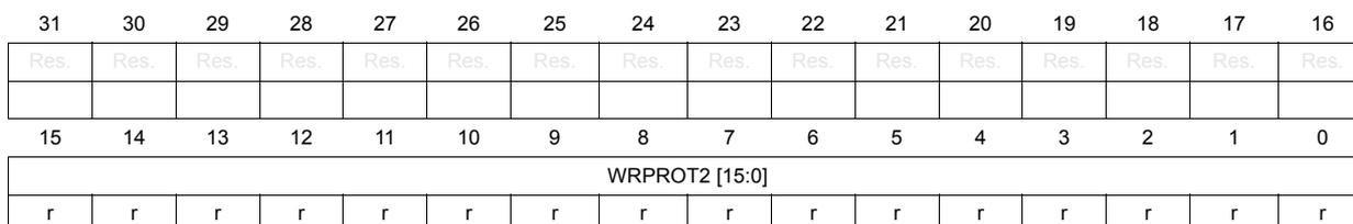
| 31 | 30 | 29 | 28 | 27 | 26 | 25 | 24 | 23 | 22 | 21 | 20 | 19 | 18 | 17 | 16 |
| Res. | Res. | Res. | Res. | Res. | Res. | Res. | Res. | Res. | Res. | Res. | Res. | Res. | Res. | Res. | Res. |
| 15 | 14 | 13 | 12 | 11 | 10 | 9 | 8 | 7 | 6 | 5 | 4 | 3 | 2 | 1 | 0 |
| WRPROT2 [15:0] | |||||||||||||||
| r | r | r | r | r | r | r | r | r | r | r | r | r | r | r | r |
Bits 31:16 Reserved, must be kept at reset value
Bits 15:0 WRPROT2 : Write protection
- – If WPRMOD = 0 in the FLASH_OPTR register, these bits contain the write protection configuration for the Flash memory (every bit protects a 4-Kbyte sector: the first bit protects the first sector, the second bit protects the second page and so on). In this case, 1 = sector protected, 0 = no protection.
- – If WPRMOD = 1, these bits are used to protect from reading as data (see Read as data and pre-read ), and then also from writing, with the same granularity and with the same combination of bits and sectors. The read protection does not protect against a fetch. In this case, 1 = no protection, 0 = sector protected.
When WPRMOD = 0, it is possible to set or reset these bits without any limitation changing the relative Option bytes.
When WPRMOD = 1, it is only possible to increase the protection, which means that the user can add zeros but cannot add ones.
The mass erase deletes the WPRMOD bits but does not delete the content of this register. After a mass erase, the user must write the relative Option bytes with zeros to remove completely the write protections.
If there is a mismatch on this configuration during the Option bytes loading, and the content of WPRMOD in the FLASH_OPTR register is:
- 1, this configuration is loaded with 0x0000.
- 0, this configuration is loaded with 0xFFFF.
If there was a mismatch when WPRMOD was loaded in the FLASH_OPTR register (thus loaded with ones), the register is loaded with 0x0000.
3.7.11 Flash register map
Table 23. Flash interface - register map and reset values
| Off-set | Register | 31 | 30 | 29 | 28 | 27 | 26 | 25 | 24 | 23 | 22 | 21 | 20 | 19 | 18 | 17 | 16 | 15 | 14 | 13 | 12 | 11 | 10 | 9 | 8 | 7 | 6 | 5 | 4 | 3 | 2 | 1 | 0 |
|---|---|---|---|---|---|---|---|---|---|---|---|---|---|---|---|---|---|---|---|---|---|---|---|---|---|---|---|---|---|---|---|---|---|
| 0x00 | FLASH_ACR | Res. | Res. | Res. | Res. | Res. | Res. | Res. | Res. | Res. | Res. | Res. | Res. | Res. | Res. | Res. | Res. | Res. | Res. | Res. | Res. | Res. | Res. | Res. | Res. | Res. | PRE_READ | DESAB_8BUF | RUN_PD | SLEEP_PD | Res. | PRFTEN | LATENCY |
| 0x00000000 | 0 | 0 | 0 | 0 | 0 | 0 | |||||||||||||||||||||||||||
| 0x004 | FLASH_PECR | Res. | Res. | Res. | Res. | Res. | Res. | Res. | Res. | NZDISABLE | Res. | Res. | Res. | Res. | OBL_LAUNCH | ERRIE | EOPIE | PARALLELBANK | Res. | Res. | Res. | Res. | FPRG | ERASE | FIX | Res. | Res. | Res. | DATA | PRG | OPTLOCK | PRGLOCK | PELOCK |
| 0x00000007 | 0 | 0 | 0 | 0 | 0 | 0 | 0 | 0 | 0 | 0 | 1 | 1 | 1 | ||||||||||||||||||||
| 0x008 | FLASH_PDKEYR | PDKEYR[31:0] | |||||||||||||||||||||||||||||||
| 0x00000000 | 0 | 0 | 0 | 0 | 0 | 0 | 0 | 0 | 0 | 0 | 0 | 0 | 0 | 0 | 0 | 0 | 0 | 0 | 0 | 0 | 0 | 0 | 0 | 0 | 0 | 0 | 0 | 0 | 0 | 0 | 0 | 0 | |
| 0x00C | FLASH_PKEYR | PKEYR[31:0] | |||||||||||||||||||||||||||||||
| 0x00000000 | 0 | 0 | 0 | 0 | 0 | 0 | 0 | 0 | 0 | 0 | 0 | 0 | 0 | 0 | 0 | 0 | 0 | 0 | 0 | 0 | 0 | 0 | 0 | 0 | 0 | 0 | 0 | 0 | 0 | 0 | 0 | 0 | |
| 0x010 | FLASH_PRGKEYR | PRGKEYR[31:0] | |||||||||||||||||||||||||||||||
| 0x00000000 | 0 | 0 | 0 | 0 | 0 | 0 | 0 | 0 | 0 | 0 | 0 | 0 | 0 | 0 | 0 | 0 | 0 | 0 | 0 | 0 | 0 | 0 | 0 | 0 | 0 | 0 | 0 | 0 | 0 | 0 | 0 | 0 | |
| 0x014 | FLASH_OPTKEYR | OPTKEYR[31:0] | |||||||||||||||||||||||||||||||
| 0x00000000 | 0 | 0 | 0 | 0 | 0 | 0 | 0 | 0 | 0 | 0 | 0 | 0 | 0 | 0 | 0 | 0 | 0 | 0 | 0 | 0 | 0 | 0 | 0 | 0 | 0 | 0 | 0 | 0 | 0 | 0 | 0 | 0 | |
| 0x018 | FLASH_SR | Res. | Res. | Res. | Res. | Res. | Res. | Res. | Res. | Res. | Res. | Res. | Res. | Res. | Res. | FWMERR | NOTZEROERR | Res. | Res. | RDERR | Res. | OPTVERR | SIZERR | PGAERR | WRPERR | Res. | Res. | Res. | Res. | READY | ENDHV | EOP | BSY |
| 0x0000000C | 0 | 0 | 0 | 0 | 0 | 0 | 0 | 1 | 1 | 0 | 0 | ||||||||||||||||||||||
| 0x01C | FLASH_OPTR | nBOOT1 | Res. | Res. | Res. | Res. | Res. | Res. | Res. | BFB2 | nRST_STBY | nRST_STOP | WDG_SW | BOR_LEV:0] | Res. | Res. | Res. | Res. | Res. | Res. | Res. | WPRMOD | RDPROT[7:0] | ||||||||||
| 0xX0XX0XXX | X | X | X | X | X | X | X | X | X | X | X | X | X | X | X | X | X | X | X | X | |||||||||||||
| 0x020 | FLASH_WRPROT1 | WRPROT1[31:0] | |||||||||||||||||||||||||||||||
| 0x0000XXXX | X | X | X | X | X | X | X | X | X | X | X | X | X | X | X | X | X | X | X | X | X | X | X | X | X | X | X | X | X | X | X | X | |
| 0x080 | FLASH_WRPROT2 | Res. | Res. | Res. | Res. | Res. | Res. | Res. | Res. | Res. | Res. | Res. | Res. | Res. | Res. | Res. | Res. | WRPROT2[15:0] | |||||||||||||||
| 0xXXXX 0000 | X | X | X | X | X | X | X | X | X | X | X | X | X | X | X | X | |||||||||||||||||
Refer to Section 2.2 on page 58 for the register boundary addresses.
3.8 Option bytes
On the NVM, an area is reserved to store a set of Option bytes which are used to configure the product. Some option bytes are written in factory while others can be configured by the end user.
The configuration managed by an end user is stored the Option bytes area (32 bytes). To be taken into account, a boot sequence must be executed. This boot sequence occurs after a power-on reset when exiting from Standby mode, or by reloading the option bytes by software ( Section 3.8.3: Reloading Option bytes by software ). The Option bytes are automatically loaded during the boot. They are used to set the content of the FLASH_OPTR and FLASH_WRPROTx registers.
Every word, when read during the boot, is interpreted as explained in Table 24 : the lower 16 bits contain the data to copy in the memory interface registers and the higher 16 bits contain the complemented value used to check that the data read are correct. If there is an error during loading operation (the higher part is not the complement of the lower one), the default value is stored in the registers. The check is done by configuration. Section 3.8.2 explains what happens when there is a mismatch on protection configurations.
During a write, no control is done to check if the higher part of a word is the complement of the lower part: this check must be performed by the user application.
Table 24. Option byte format
| 31-24 | 23-16 | 15-8 | 7-0 |
|---|---|---|---|
| Complemented Option byte 1 | Complemented Option byte 0 | Option byte 1 | Option byte 0 |
3.8.1 Option bytes description
The Option bytes can be read from the memory locations listed in Table 25 .
Table 25. Option byte organization
| Address | [31:16] | [15:0] |
|---|---|---|
| 0x1FF8 0000 | nFLASH_OPTR[15:0] | FLASH_OPTR[15:0] |
| 0x1FF8 0004 | nFLASH_OPTR[31:16] | FLASH_OPTR[31:16] |
| 0x1FF8 0008 | nFLASH_WRPROT1[15:0] | FLASH_WRPROT1[15:0] |
| 0x1FF8 000C | nFLASH_WRPROT1[31:16] | FLASH_WRPROT1[31:16] |
| 0x1FF8 0010 | nFLASH_WRPROT2[15:0] | FLASH_WRPROT2[15:0] |
Refer to Section 3.7.8: Option bytes register (FLASH_OPTR) and Section 3.7.9: Write protection register 1 (FLASH_WRPROT1) for the meaning of each bit.
3.8.2 Mismatch when loading protection flags
When there is a mismatch during an Option byte loading, the memory interface sets the default value in registers.
In the Option byte area, there are three kinds of protection information:
- •
RDPROT
This configuration sets the Protection Level. As explained in the next section, changing this level changes the possibility to access the NVM and the product. The default value is Level 1. It is possible to return to Level 0 from Level 1 but all content of the data EEPROM and Flash program memory will be deleted (mass erase). It is always possible to move to Level 2, but not to change protection levels when Level 2 is loaded (if the user writes in Option bytes a Level 2 but never reloads the Option bytes, the memory interface continues to work in the previous level and it is possible to write again a different protection level in the Option bytes area). - •
WPRMOD
This flag is independent from RDPROT and set if the Flash program memory is protected from read or write. When this flag is 1 (read protection), the only way to reset it is to request a mass erase (also returning to Level 0). This means that there is no way to remove the read protection when the device is in Level 2. The default value is 1 (read protection) and a mismatch on this bit also generates the default value for the WRPROT configuration. - •
WRPROT
This configuration sets which sectors of the Flash program memory are read- or write-protected. If the read protection is disabled (WPRMOD = 0), 1 must be set in the right bit to protect a sector. If the read protection is enabled (WPRMOD = 1), 0 must be in the right bit to protect a sector. If during boot there is a mismatch on WPRMOD, this configuration is loaded with zeros so that all sectors of the Flash program memory are protected from read. If WPRMOD has been read correctly but there is a mismatch reading WRPROT, the register will be loaded with zeros if WPRMOD = 1, and with ones if WPRMOD = 0.
Thus, a mismatch on a protection can have a serious impact on the normal execution of code (if it is in the Flash program memory): when there is a read protection, only a fetch is possible. In the Flash program memory, some values are read as data (the constants, for example) during a code execution; protecting all sectors from read prevents the execution of the application code from the Flash program memory.
3.8.3 Reloading Option bytes by software
It is possible to request an Option byte reloading by setting the OBL_LAUNCH flag to 1 in the FLASH_PECR register. This bit can be set only when OPTLOCK = 0 (and PELOCK = 0). Setting this bit, the ongoing write/erase is completed, but no new write/erase or read operation is executed.
The reload of Option bytes generates a reset of the device but without a power-down. The options must be reloaded after every change of the Option bytes in the NVM, so that the changes can apply. It is possible to reload by setting OBL_LAUNCH, or with a power-on of the V18 domain (i.e. after a power-on reset or after a standby).