14. Comparator (COMP)
14.1 Introduction
STM32F3xx devices embed three comparators, COMP2, COMP4 and COMP6 that can be used either as standalone devices (all terminals are available on I/Os) or combined with the timers.
The comparators can be used for a variety of functions including:
- • Wake-up from low-power mode triggered by an analog signal,
- • Analog signal conditioning,
- • Cycle-by-cycle current control loop when combined with the DAC and a PWM output from a timer.
14.2 COMP main features
- • Rail-to-rail comparators
- • Each comparator has positive and configurable negative inputs used for flexible voltage selection:
- – Multiplexed I/O pins
- – DAC1 channel 1
- – Internal reference voltage and three submultiple values (1/4, 1/2, 3/4) provided by scaler (buffered voltage divider)
- • The outputs can be redirected to an I/O or to timer inputs for triggering:
- – Capture events
- – OCREF_CLR events (for cycle-by-cycle current control)
- – Break events for fast PWM shutdowns
- • Each comparator has interrupt generation capability with wake-up from Sleep and Stop modes (through the EXTI controller)
14.3 COMP functional description
14.3.1 COMP block diagram
The block diagrams of COMP2, COMP4 and COMP6 are shown in following figures:
Figure 77. Comparator 2 block diagram
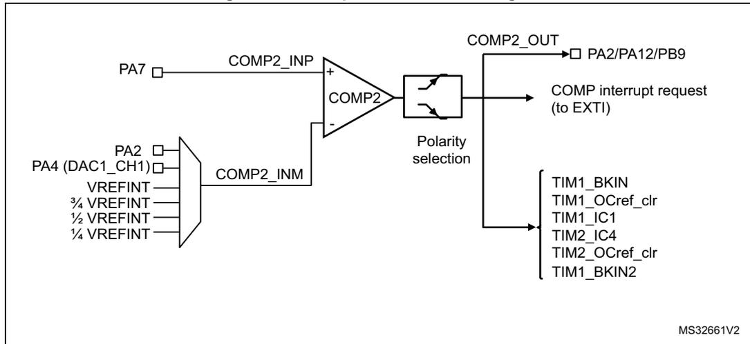
The diagram shows the internal structure of Comparator 2 (COMP2). The non-inverting input (COMP2_INP) is connected to pin PA7. The inverting input (COMP2_INM) is connected to a multiplexer that selects between several sources: PA2, PA4 (DAC1_CH1), VREFINT, 3/4 VREFINT, 1/2 VREFINT, and 1/4 VREFINT. The output of the comparator passes through a 'Polarity selection' block. The output signal, COMP2_OUT, is available at pins PA2/PA12/PB9. The output also generates a 'COMP interrupt request (to EXTI)' and is connected to a list of timer inputs: TIM1_BKIN, TIM1_OCref_clr, TIM1_IC1, TIM2_IC4, TIM2_OCref_clr, and TIM1_BKIN2. The identifier MS32661V2 is shown in the bottom right corner.
Figure 78. Comparator 4 block diagram
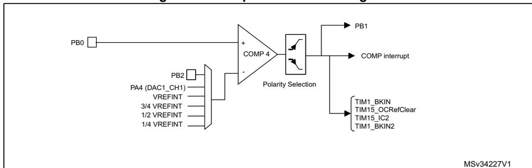
The diagram shows the internal structure of Comparator 4 (COMP4). The non-inverting input is connected to pin PB0. The inverting input is connected to a multiplexer that selects between PB2, PA4 (DAC1_CH1), VREFINT, 3/4 VREFINT, 1/2 VREFINT, and 1/4 VREFINT. The output passes through a 'Polarity Selection' block. The output signal is available at pin PB1 and generates a 'COMP interrupt'. It is also connected to a list of timer inputs: TIM1_BKIN, TIM15_OCRefClear, TIM15_IC2, and TIM1_BKIN2. The identifier MSv34227V1 is shown in the bottom right corner.
Figure 79. Comparator 6 block diagram
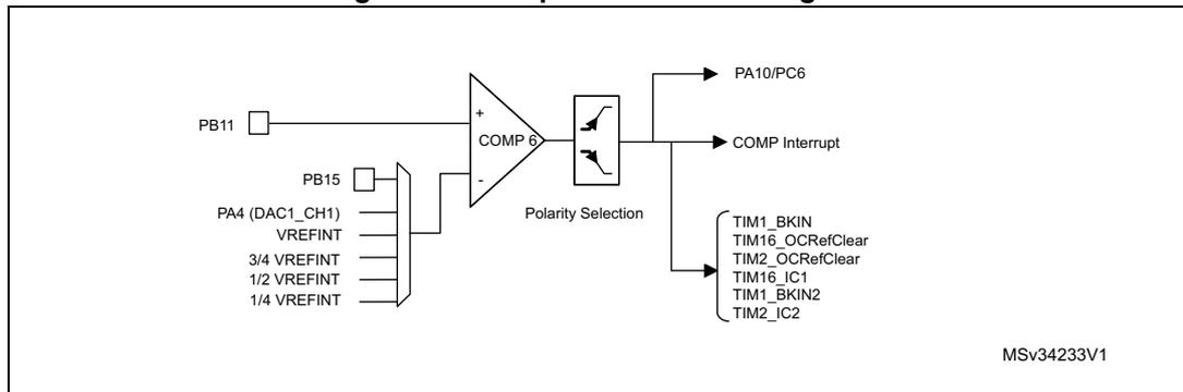
The diagram shows the internal structure of Comparator 6 (COMP6). The non-inverting input is connected to pin PB11. The inverting input is connected to a multiplexer that selects between PB15, PA4 (DAC1_CH1), VREFINT, 3/4 VREFINT, 1/2 VREFINT, and 1/4 VREFINT. The output passes through a 'Polarity Selection' block. The output signal is available at pins PA10/PC6 and generates a 'COMP interrupt'. It is also connected to a list of timer inputs: TIM1_BKIN, TIM16_OCRefClear, TIM2_OCRefClear, TIM16_IC1, TIM1_BKIN2, and TIM2_IC2. The identifier MSv34233V1 is shown in the bottom right corner.
14.3.2 COMP pins and internal signals
The I/Os used as comparators inputs must be configured in analog mode in the GPIOs registers.
The comparator output can be connected to the I/Os using the alternate function channel given in “Alternate function mapping” table in the datasheet.
The table below summarizes the I/Os that can be used as comparators inputs and outputs.
The output can also be internally redirected to a variety of timer input for the following purposes:
- • Emergency shut-down of PWM signals, using BKIN and BKIN2 inputs
- • Cycle-by-cycle current control, using OCREF_CLR inputs
- • Input capture for timing measures
It is possible to have the comparator output simultaneously redirected internally and externally.
Table 48. STM32F3xx comparator input/outputs summary
| - | Comparator input/outputs | ||
|---|---|---|---|
| COMP2 | COMP4 | COMP6 | |
| Comparator inverting Input: connection to internal signals | DAC1_CH1 VREFINT Vrefint \( \frac{3}{4} \) Vrefint \( \frac{1}{2} \) Vrefint \( \frac{1}{4} \) Vrefint | ||
| Comparator Inputs connected to I/Os (+: non inverting input; -: inverting input) | +: PA7 -: PA2 | +: PB0 -: PB2 | +: PB11 -: PB15 |
| Comparator outputs (motor control protection) | T1BKIN T1BKIN2 | ||
| Outputs on I/Os | PA2 PA12 PB9 | PB1 | PA10 PC6 |
| Outputs to internal signals | TIM1_OCREF_CLR TIM1_IC1 TIM2_IC4 TIM2_OCREF_CLR | TIM15_OCREF_CLR TIM15_IC2 | TIM2_IC2 TIM2_OCREF_CLR TIM16_OCREF_CLR TIM16_IC1 |
14.3.3 COMP reset and clocks
The COMP clock provided by the clock controller is synchronous with the PCLK2 (APB2 clock).
There is no clock enable control bit provided in the RCC controller. Reset and clock enable bits are common for COMP and SYSCFG. To use a clock source for the comparator, the SYSCFG clock enable control bit must be set in the RCC controller.
Important: The polarity selection logic and the output redirection to the port works independently from the PCLK2 clock. This allows the comparator to work even in Stop mode.
14.3.4 Comparator LOCK mechanism
The comparators can be used for safety purposes, such as over-current or thermal protection. For applications having specific functional safety requirements, it is necessary to insure that the comparator programming cannot be altered in case of spurious register access or program counter corruption.
For this purpose, the comparator control and status registers can be write-protected (read-only).
Once the programming is completed, using bits 30:0 of COMPx_CSR, the COMPx LOCK bit can be set to 1. This causes the whole COMP_CSR register to become read-only, including the COMPx LOCK bit.
The write protection can only be reset by a MCU reset.
14.3.5 Comparator output blanking function
The purpose of the blanking function is to prevent the current regulation to trip upon short current spikes at the beginning of the PWM period (typically the recovery current in power switches anti parallel diodes). It consists of a selection of a blanking window which is a timer output compare signal. The selection is done by software (refer to the comparator register description for possible blanking signals). Then, the complementary of the blanking signal is ANDed with the comparator output to provide the wanted comparator output. See the example provided in the figure below.
Figure 80. Comparator output blanking
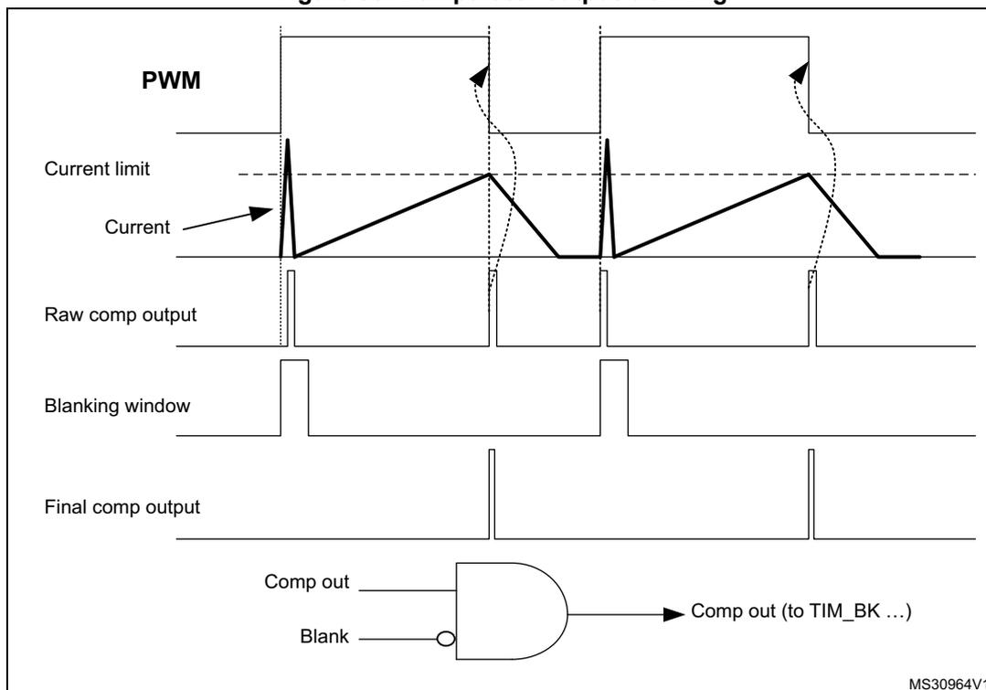
The diagram shows the following signals over time:
- PWM: A periodic square wave signal.
- Current limit: A dashed horizontal line representing the maximum current threshold.
- Current: A signal that rises sharply when PWM is high, reaching the current limit, and then decays when PWM is low.
- Raw comp output: A signal that pulses when the current exceeds the current limit.
- Blanking window: A signal that is high during the PWM transition periods.
- Final comp output: The output after blanking, which is the result of an AND gate with inputs 'Comp out' and 'Blank' (inverted).
Logic: Comp out (to TIM_BK ...) = Comp out AND NOT (Blank)
MS30964V1
14.4 COMP interrupts
The comparator outputs are internally connected to the Extended interrupts and events controller. Each comparator has its own EXTI line and can generate either interrupts or events. The same mechanism is used to exit from low-power modes.
Refer to Interrupt and events section for more details.
14.5 COMP registers
14.5.1 COMP2 control and status register (COMP2_CSR)
Address offset: 0x20
Reset value: 0x0000 0000
| 31 | 30 | 29 | 28 | 27 | 26 | 25 | 24 | 23 | 22 | 21 | 20 | 19 | 18 | 17 | 16 |
|---|---|---|---|---|---|---|---|---|---|---|---|---|---|---|---|
| COMP2LOCK | COMP2OUT | Res. | Res. | COMP2_BLANKING[2:0] | Res. | ||||||||||
| rwo | r | rw | rw | rw | rw | rw | |||||||||
| 15 | 14 | 13 | 12 | 11 | 10 | 9 | 8 | 7 | 6 | 5 | 4 | 3 | 2 | 1 | 0 |
|---|---|---|---|---|---|---|---|---|---|---|---|---|---|---|---|
| COMP2POL | Res. | COMP2OUTSEL[3:0] | Res. | COMP2INMSEL[2:0] | Res. | COMP2_INP_D_AC | COMP2_EN | ||||||||
| rw | rw | rw | rw | rw | rw | rw | rw | rw | rw | ||||||
This bit is write-once. It is set by software. It can only be cleared by a system reset.
It allows to have COMP2_CSR register as read-only.
0: COMP2_CSR is read-write.
1: COMP2_CSR is read-only.
Bit 30 COMP2OUT: Comparator 2 outputThis read-only bit is a copy of comparator 1 output state.
0: Output is low (non-inverting input below inverting input).
1: Output is high (non-inverting input above inverting input).
Bits 29:21 Reserved, must be kept at reset value.
Bits 20:18 COMP2_BLANKING[2:0]: Comparator 2 output blanking sourceThese bits select which Timer output controls the comparator 1 output blanking.
000: No blanking
001: TIM1_OC5 selected as blanking source
010: TIM2_OC3 selected as blanking source
Other configurations: reserved
Bits 17:16 Reserved, must be kept at reset value.
Bit 15 COMP2POL: Comparator 2 output polarityThis bit is used to invert the comparator 2 output.
0: Output is not inverted
1: Output is inverted
Bit 14 Reserved, must be kept at reset value.
Bits 13:10 COMP2OUTSEL[3:0]: Comparator 2 output selectionThese bits select which Timer input must be connected with the comparator2 output.
0000: No selection
0001: (BRK_ACTH) Timer 1 break input
0010: (BRK2) Timer 1 break input 2
0101: Timer 1 break input2
0110: Timer 1 OCREF_CLR input
0111: Timer 1 input capture 1
1000: Timer 2 input capture 4
1001: Timer 2 OCREF_CLR input
Bits 9:7 Reserved, must be kept at reset value.
Bits 6:4 COMP2INMSEL[2:0] : Comparator 2 inverting input selection
These bits allows to select the source connected to the inverting input of the comparator 2.
000: 1/4 of Vrefint
001: 1/2 of Vrefint
010: 3/4 of Vrefint
011: Vrefint
100: PA4 or DAC1_CH1 output if enabled
110: PA2
Remaining combinations: reserved.
Bit 1 COMP2_INP_DAC : Comparator 2 non inverting input connection to DAC output.
This bit closes a switch between comparator 2 non-inverting input and DAC out I/O.
0: Switch open
1: Switch closed
This switch is solely intended to redirect signals onto high impedance input, such as COMP2 non-inverting input (highly resistive switch)
Bit 0 COMP2EN : Comparator 2 enable
This bit switches COMP2 ON/OFF.
0: Comparator 2 disabled
1: Comparator 2 enabled
14.5.2 COMP4 control and status register (COMP4_CSR)
Address offset: 0x28
Reset value: 0x0000 0000
| 31 | 30 | 29 | 28 | 27 | 26 | 25 | 24 | 23 | 22 | 21 | 20 | 19 | 18 | 17 | 16 |
|---|---|---|---|---|---|---|---|---|---|---|---|---|---|---|---|
| COMP4LOCK | COMP4OUT | Res. | Res. | COMP4_BLANKING[2:0] | Res. | ||||||||||
| rwo | r | rw | rw | rw | rw | rw | |||||||||
| 15 | 14 | 13 | 12 | 11 | 10 | 9 | 8 | 7 | 6 | 5 | 4 | 3 | 2 | 1 | 0 |
|---|---|---|---|---|---|---|---|---|---|---|---|---|---|---|---|
| COMP4POL | Res. | COMP4OUTSEL[3:0] | Res. | Res. | COMP4INMSEL[2:0] | Res. | COMP4EN | ||||||||
| rw | rw | rw | rw | rw | rw | rw | rw | rw | |||||||
Bit 31 COMP4LOCK : Comparator 4 lock
This bit is write-once. It is set by software. It can only be cleared by a system reset.
It allows to have COMP4_CSR register as read-only.
0: COMP4_CSR is read-write.
1: COMP4_CSR is read-only.
Bit 30 COMP4OUT : Comparator 4 output
This read-only bit is a copy of comparator 4 output state.
0: Output is low (non-inverting input below inverting input).
1: Output is high (non-inverting input above inverting input).
Bits 29: Reserved, must be kept at reset value.
Bits 20:18 COMP4_BLANKING : Comparator 4 blanking source
These bits select which Timer output controls the comparator 4 output blanking.
000: No blanking
011: TIM15_OC1 selected as blanking source
Other configurations: reserved, must be kept at reset value
Bits 17:16 Reserved, must be kept at reset value.
Bit 15 COMP4POL : Comparator 4 output polarity
This bit is used to invert the comparator 4 output.
0: Output is not inverted
1: Output is inverted
Bit 14 Reserved, must be kept at reset value.
Bits 13:10 COMP4OUTSEL[3:0] : Comparator 4 output selection
These bits select which Timer input must be connected with the comparator4 output.
0000: No timer input selected
0001: (BRK) Timer 1 break input
0010: (BRK2) Timer 1 break input 2
0101: Timer 1 break input 2
1000: Timer 15 input capture 2
1010: Timer 15 OCREF_CLR input
Remaining combinations: reserved.
Bits 9:7 Reserved, must be kept at reset value.
Bits 6:4 COMP4INMSEL[2:0] : Comparator 4 inverting input selection
These bits allows to select the source connected to the inverting input of the comparator 4.
000: 1/4 of Vrefint
001: 1/2 of Vrefint
010: 3/4 of Vrefint
011: Vrefint
100: PA4 or DAC1_CH1 output if enabled
111: PB2
Remaining combinations: reserved.
Bits 3:1 Reserved, must be kept at reset value.
Bit 0 COMP4EN : Comparator 4 enable
This bit switches COMP4 ON/OFF.
0: Comparator 4 disabled
1: Comparator 4 enabled
14.5.3 COMP6 control and status register (COMP6_CSR)
Address offset: 0x30
Reset value: 0x0000 0000
| 31 | 30 | 29 | 28 | 27 | 26 | 25 | 24 | 23 | 22 | 21 | 20 | 19 | 18 | 17 | 16 |
|---|---|---|---|---|---|---|---|---|---|---|---|---|---|---|---|
| COMP6LOCK | COMP6OUT | Res. | Res. | Res. | Res. | Res. | Res. | Res. | Res. | Res. | COMP6_BLANKING[2:0] | Res. | |||
| r/w | r | r/w | r/w | r/w | r/w | r/w | |||||||||
| 15 | 14 | 13 | 12 | 11 | 10 | 9 | 8 | 7 | 6 | 5 | 4 | 3 | 2 | 1 | 0 |
|---|---|---|---|---|---|---|---|---|---|---|---|---|---|---|---|
| COMP 6POL | Res. | COMP6OUTSEL[3:0] | Res. | Res. | Res. | COMP6INMSEL[2:0] | Res. | Res. | COMP6 EN | ||||||
| rw | rw | rw | rw | rw | rw | rw | rw | rw | |||||||
Bit 31 COMP6LOCK : Comparator 6 lock
This bit is write-once. It is set by software. It can only be cleared by a system reset.
It allows to have COMP6_CSR register as read-only.
0: COMP6_CSR is read-write.
1: COMP6_CSR is read-only.
Bit 30 COMP6OUT : Comparator 6 output
This read-only bit is a copy of comparator 6 output state.
0: Output is low (non-inverting input below inverting input).
1: Output is high (non-inverting input above inverting input).
Bits 29: Reserved, must be kept at reset value.
Bits 20:18 COMP6_BLANKING : Comparator 6 blanking source
These bits select which Timer output controls the comparator 6 output blanking.
000: No blanking
011: TIM2_OC4 selected as blanking source
100: TIM15_OC2 selected as blanking source
Other configurations: reserved
The blanking signal is active high (masking comparator output signal). It is up to the user to program the comparator and blanking signal polarity correctly.
Bits 17:16 Reserved, must be kept at reset value.
Bit 15 COMP6POL : Comparator 6 output polarity
This bit is used to invert the comparator 6 output.
0: Output is not inverted
1: Output is inverted
Bit 14 Reserved, must be kept at reset value.
Bits 13:10 COMP6OUTSEL[3:0] : Comparator 6 output selection
These bits select which Timer input must be connected with the comparator 6 output.
0000: No timer input
0001: (BRK_ACTH) Timer 1 break input
0010: (BRK2) Timer 1 break input 2
0101: Timer 1 break input 2
0110: Timer 2 input capture 2
1000: Timer 2 OCREF_CLR input
1001: Timer 16 OCREF_CLR input
1010: Timer 16 input capture 1
Remaining combinations: reserved.
Bits 9:7 Reserved, must be kept at reset value.
Bits 6:4 COMP6INMSEL[2:0] : Comparator 6 inverting input selection
These bits allows to select the source connected to the inverting input of the comparator 6.
000: 1/4 of Vrefint
001: 1/2 of Vrefint
010: 3/4 of Vrefint
011: Vrefint
100: PA4 or DAC1_CH1 output if enabled
111: PB15
Remaining combinations: reserved.
Bits 3:1 Reserved, must be kept at reset value.
Bit 0 COMP6EN : Comparator 6 enable
This bit switches COMP6 ON/OFF.
0: Comparator 6 disabled
1: Comparator 6 enabled
14.5.4 COMP register map
The following table summarizes the comparator registers.
Table 49. COMP register map and reset values
| Offset | Register | 31 | 30 | 29 | 28 | 27 | 26 | 25 | 24 | 23 | 22 | 21 | 20 | 19 | 18 | 17 | 16 | 15 | 14 | 13 | 12 | 11 | 10 | 9 | 8 | 7 | 6 | 5 | 4 | 3 | 2 | 1 | 0 | |
|---|---|---|---|---|---|---|---|---|---|---|---|---|---|---|---|---|---|---|---|---|---|---|---|---|---|---|---|---|---|---|---|---|---|---|
| 0x20 | COMP2_CSR | COMP2LOCK | COMP2OUT | Res. | Res. | Res. | Res. | Res. | Res. | Res. | Res. | Res. | COMP2_BLANKING | Res. | COMP2POL | Res. | COMP2OUTSEL[3:0] | Res. | Res. | Res. | COMP2INMSEL[2:0] | Res. | Res. | COMP2_INP_DAC | COMP2EN | |||||||||
| Reset value | 0 | 0 | 0 | 0 | 0 | 0 | 0 | 0 | 0 | 0 | 0 | 0 | 0 | 0 | ||||||||||||||||||||
| 0x28 | COMP4_CSR | COMP4LOCK | COMP4OUT | Res. | Res. | Res. | Res. | Res. | Res. | Res. | Res. | Res. | COMP4_BLANKING | Res. | COMP4POL | Res. | COMP4OUTSEL[3:0] | Res. | Res. | Res. | COMP4INMSEL[2:0] | Res. | Res. | COMP4EN | ||||||||||
| Reset value | 0 | 0 | 0 | 0 | 0 | 0 | 0 | 0 | 0 | 0 | 0 | 0 | 0 | 0 | ||||||||||||||||||||
| 0x30 | COMP6_CSR | COMP6LOCK | COMP6OUT | Res. | Res. | Res. | Res. | Res. | Res. | Res. | Res. | Res. | COMP6_BLANKING | Res. | COMP6POL | Res. | COMP6OUTSEL[3:0] | Res. | Res. | Res. | COMP6INMSEL[2:0] | Res. | Res. | COMP6EN | ||||||||||
| Reset value | 0 | 0 | 0 | 0 | 0 | 0 | 0 | 0 | 0 | 0 | 0 | 0 | 0 | 0 | ||||||||||||||||||||
Refer to Section 2.2 on page 40 for the register boundary addresses.