2. System and memory overview
2.1 System architecture
The STM32F318x8 main system consists of:
- • Four masters:
- – Cortex ® -M4 core I-bus
- – Cortex ® -M4 core D-bus
- – Cortex ® -M4 core S-bus
- – DMA1 (general-purpose DMA)
- • Six slaves:
- – Internal flash memory on the DCode
- – Internal flash memory on ICode
- – Up to 16-Kbyte internal SRAM
- – AHB to APBx (APB1 or APB2), which connect all the APB peripherals
- – AHB dedicated to GPIO ports
- – ADC1
The interconnection uses a multilayer AHB bus architecture as shown in figures 1.
Figure 1. System architecture
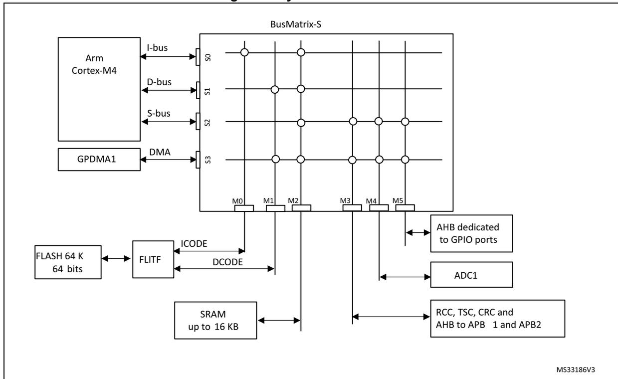
The diagram illustrates the system architecture of the STM32F318x8. At the top left, the 'Arm Cortex-M4' core is shown with three output buses: 'I-bus', 'D-bus', and 'S-bus'. Below it, 'GP DMA1' is shown with a 'DMA' output. Both sets of outputs connect to a central 'BusMatrix-S' block. This matrix is a grid with six horizontal lines (labeled M0 to M5 at the bottom) and six vertical lines. Connections are indicated by dots at the intersections. Below the matrix, the following components are connected to the horizontal lines:
- 'FLASH 64 K 64 bits' connects to 'FLITF', which then connects to the matrix via 'ICODE' (on line M0) and 'DCODE' (on line M1).
- 'SRAM up to 16 KB' connects directly to line M2.
- 'RCC, TSC, CRC and AHB to APB 1 and APB2' connects to line M3.
- 'ADC1' connects to line M4.
- 'AHB dedicated to GPIO ports' connects to line M5.
2.1.1 S0: I-bus
This bus connects the instruction bus of the Cortex ® -M4 core to the BusMatrix. This bus is used by the core to fetch instructions. The targets of this bus are the internal Flash memory and the SRAM up to 16 Kbytes.
2.1.2 S1: D-bus
This bus connects the DCode bus (literal load and debug access) of the Cortex ® -M4 core to the BusMatrix. The targets of this bus are the internal Flash memory and the SRAM (16 Kbytes).
2.1.3 S2: S-bus
This bus connects the system bus of the Cortex ® -M4 core to the BusMatrix. This bus is used to access data located in the peripheral or SRAM area. The targets of this bus are the SRAM (16 Kbytes), the AHB to APB1/APB2 bridges, the AHB IO port and the ADC.
2.1.4 S3: DMA-bus
This bus connects the AHB master interface of the DMA to the BusMatrix, which manages the access of different Masters to flash, SRAM, and peripherals.
2.1.5 BusMatrix
The BusMatrix manages the access arbitration between Masters. The arbitration uses a Round Robin algorithm. The BusMatrix is composed of five masters (CPU AHB, System bus, DCode bus, ICode bus, DMA1 bus) and seven slaves (FLITF, SRAM, AHB2GPIO and AHB2APB1/2 bridges, and ADC).
AHB/APB bridges
The two AHB/APB bridges provide full synchronous connections between the AHB and the two APB buses. APB1 is limited to 36 MHz. APB2 operates at full speed (72 MHz).
Refer to Section 2.2: Memory organization on page 40 for the address mapping of the peripherals connected to this bridge.
After each device reset, all peripheral clocks are disabled (except for the SRAM and FLITF). Before using a peripheral the user has to enable its clock in the RCC_AHBENR, RCC_APB2ENR or RCC_APB1ENR register.
When a 16- or 8-bit access is performed on an APB register, the access is transformed into a 32-bit access: the bridge duplicates the 16- or 8-bit data to feed the 32-bit vector.
2.2 Memory organization
2.2.1 Introduction
Program memory, data memory, registers and I/O ports are organized within the same linear 4-Gbyte address space.
The bytes are coded in memory in Little Endian format. The lowest numbered byte in a word is considered the word's least significant byte and the highest numbered byte the most significant.
The addressable memory space is divided into eight main blocks, of 512 Mbytes each.
2.2.2 Memory map and register boundary addresses
All the memory map areas that are not allocated to on-chip memories and peripherals are considered “Reserved”. For the detailed mapping of available memory and register areas, refer to the following table.
The following table gives the boundary addresses of the peripherals available in the devices.
Table 1. STM32F3xx peripheral register boundary addresses (1)| Bus | Boundary address | Size (bytes) | Peripheral | Peripheral register map |
|---|---|---|---|---|
| AHB3 | 0x5000 0000 - 0x5000 03FF | 1 K | ADC1 | Section 12.7 on page 274 |
| - | 0x4800 1800 - 0x4FFF FFFF | ~132 M | Reserved | - |
| AHB2 | 0x4800 1400 - 0x4800 17FF | 1 K | GPIOF | Section 8.4.12 on page 142 |
| 0x4800 1000 - 0x4800 13FF | 1 K | Reserved | - | |
| 0x4800 0C00 - 0x4800 0FFF | 1 K | GPIOE | Section 8.4.12 on page 142 | |
| 0x4800 0800 - 0x4800 0BFF | 1 K | GPIOC | ||
| 0x4800 0400 - 0x4800 07FF | 1 K | GPIOB | ||
| 0x4800 0000 - 0x4800 03FF | 1 K | GPIOA | ||
| - | 0x4002 4400 - 0x47FF FFFF | ~128 M | Reserved | |
| AHB1 | 0x4002 4000 - 0x4002 43FF | 1 K | TSC | Section 16.6.11 on page 329 |
| 0x4002 3400 - 0x4002 3FFF | 3 K | Reserved | - | |
| 0x4002 3000 - 0x4002 33FF | 1 K | CRC | Section 5.4.6 on page 74 | |
| 0x4002 2400 - 0x4002 2FFF | 3 K | Reserved | - | |
| 0x4002 2000 - 0x4002 23FF | 1 K | Flash interface | Section 3.6 on page 63 | |
| 0x4002 1400 - 0x4002 1FFF | 3 K | Reserved | - | |
| 0x4002 1000 - 0x4002 13FF | 1 K | RCC | Section 7.4.14 on page 124 | |
| 0x4002 0400 - 0x4002 0FFF | 3 K | Reserved | - | |
| 0x4002 0000 - 0x4002 03FF | 1 K | DMA1 | Section 10.6.7 on page 172 | |
| - | 0x4001 8000 - 0x4001 FFFF | 32 K | Reserved | - |
| APB2 | 0x4001 4C00 - 0x4001 7FFF | 13 K | Reserved | - |
| 0x4001 4800 - 0x4001 4BFF | 1 K | TIM17 | Section 19.6.18 on page 573 | |
| 0x4001 4400 - 0x4001 47FF | 1 K | TIM16 | ||
| 0x4001 4000 - 0x4001 43FF | 1 K | TIM15 | Section 19.5.19 on page 553 | |
| 0x4001 3C00 - 0x4001 3FFF | 1 K | Reserved | - | |
| 0x4001 3800 - 0x4001 3BFF | 1 K | USART1 | Section 26.8.12 on page 778 | |
| 0x4001 3000 - 0x4001 37FF | 2 K | Reserved | - | |
| 0x4001 2C00 - 0x4001 2FFF | 1 K | TIM1 | Section 17.4.27 on page 423 | |
| 0x4001 0800 - 0x4001 0BFF | 8 K | Reserved | - | |
| 0x4001 0400 - 0x4001 07FF | 1 K | EXTI | Section 11.3.13 on page 191 | |
| 0x4001 0000 - 0x4001 03FF | 1 K | SYSCFG + COMP + OPAMP | Section 9.1.7 on page 151 Section 14.5.4 on page 302 Section 15.4.2 on page 312 | |
| - | 0x4000 9C00 - 0x4000 FFFF | 25 K | Reserved | - |
| Bus | Boundary address | Size (bytes) | Peripheral | Peripheral register map |
|---|---|---|---|---|
| APB1 | 0x4000 7C00 - 0x4000 9BFF | 8 K | Reserved | - |
| 0x4000 7800 - 0x4000 7BFF | 1 K | I2C3 | Section 25.9.12 on page 711 | |
| 0x4000 7400 - 0x4000 77FF | 1 K | DAC1 | Section 13.9.8 on page 291 | |
| 0x4000 7000 - 0x4000 73FF | 1 K | PWR | Section 6.4.3 on page 89 | |
| 0x4000 5C00 - 0x4000 6FFF | 5 K | Reserved | - | |
| 0x4000 5800 - 0x4000 5BFF | 1 K | I2C2 | Section 25.9.12 on page 711 | |
| 0x4000 5400 - 0x4000 57FF | 1 K | I2C1 | ||
| 0x4000 4C00 - 0x4000 53FF | 2 K | Reserved | - | |
| 0x4000 4800 - 0x4000 4BFF | 1 K | USART3 | Section 26.8.12 on page 778 | |
| 0x4000 4400 - 0x4000 47FF | 1 K | USART2 | ||
| 0x4000 4000 - 0x4000 43FF | 1 K | I2S3ext | Section 27.9.10 on page 836 | |
| 0x4000 3C00 - 0x4000 3FFF | 1 K | SPI3/I2S3 | ||
| 0x4000 3800 - 0x4000 3BFF | 1 K | SPI2/I2S2 | ||
| 0x4000 3400 - 0x4000 37FF | 1 K | I2S2ext | ||
| 0x4000 3000 - 0x4000 33FF | 1 K | IWDG | Section 23.4.6 on page 603 | |
| 0x4000 2C00 - 0x4000 2FFF | 1 K | WWDG | Section 22.5.4 on page 594 | |
| 0x4000 2800 - 0x4000 2BFF | 1 K | RTC | Section 24.6.20 on page 645 | |
| 0x4000 1400 - 0x4000 27FF | 5 K | Reserved | - | |
| 0x4000 1000 - 0x4000 13FF | 1 K | TIM6 | Section 20.4.9 on page 587 | |
| 0x4000 0400 - 0x4000 0FFF | 3 K | Reserved | - | |
| 0x4000 0000 - 0x4000 03FF | 1 K | TIM2 | Section 18.4.22 on page 494 | |
| - | 0x2000 4000 - 3FFF FFFF | ~512 M | Reserved | - |
| - | 0x2000 0000 - 0x2000 3FFF | 16 K | SRAM | - |
| - | 0x1FFF F800 - 0x1FFF FFFF | 2 K | Option bytes | - |
| - | 0x1FFF D800 - 0x1FFF F7FF | 8 K | System memory | - |
| - | 0x0801 0000 - 0x1FFF D7FF | ~384 M | Reserved | - |
| - | 0x0800 0000 - 0x0800 FFFF | 64 K | Main Flash memory | - |
| - | 0x0001 0000 - 0x07FF FFFF | ~128 M | Reserved | - |
| - | 0x0000 000 - 0x0000 FFFF | 64 K | Main Flash memory, system memory or SRAM depending on BOOT configuration | - |
1. The gray color is used for reserved Flash memory addresses.
2.3 Embedded SRAM
STM32F3xx devices feature up to 16 Kbytes of static SRAM. It can be accessed as bytes, halfwords (16 bits) or full words (32 bits). Up to 16 Kbytes of SRAM can be addressed at maximum system clock frequency without wait state, and can be accessed by both CPU and DMA.
2.4 Flash memory overview
The Flash memory is composed of two distinct physical areas:
- • The main Flash memory block. It contains the application program and user data if necessary.
- • The information block. It is composed of two parts:
- – Option bytes for hardware and memory protection user configuration.
- – System memory which contains the proprietary boot loader code. Please, refer to Section 3: Embedded flash memory for more details.
Flash memory instructions and data access are performed through the AHB bus. The prefetch block is used for instruction fetches through the ICode bus. Arbitration is performed in the Flash memory interface, and priority is given to data access on the DCode bus. It also implements the logic necessary to carry out the Flash memory operations (Program/Erase) controlled through the Flash registers.
2.5 Boot configuration
In the STM32F3xx, three different boot modes can be selected through the BOOT0 pin and nBOOT1 bit in the User option byte, as shown in the following table:
Table 2. Boot modes
| Boot mode selection | Boot mode | Aliasings | |
|---|---|---|---|
| nBOOT1 | BOOT0 | - | - |
| x | 0 | Main Flash memory | Main flash memory is selected as boot area |
| 1 | 1 | System memory | System memory is selected as boot area |
| 0 | 1 | Embedded SRAM | Embedded SRAM (on the DCode bus) is selected as boot area |
The values on both BOOT0 pin and nBOOT1 bit are latched on the 4th rising edge of SYSCLK after a reset.
It is up to the user to set the nBOOT1 and BOOT0 to select the required boot mode. The BOOT0 pin and nBOOT1 bit are also resampled when exiting from Standby mode. Consequently they must be kept in the required Boot mode configuration in Standby mode. After this startup delay has elapsed, the CPU fetches the top-of-stack value from address 0x0000 0000, then starts code execution from the boot memory at 0x0000 0004. Depending
on the selected boot mode, main Flash memory, system memory or SRAM is accessible as follows:
- • Boot from main Flash memory: the main Flash memory is aliased in the boot memory space (0x0000 0000), but still accessible from its original memory space (0x0800 0000). In other words, the Flash memory contents can be accessed starting from address 0x0000 0000 or 0x0800 0000.
- • Boot from system memory: the system memory is aliased in the boot memory space (0x0000 0000), but still accessible from its original memory space (0x1FFF D800).
- • Boot from the embedded SRAM: the SRAM is aliased in the boot memory space (0x0000 0000), but it is still accessible from its original memory space (0x2000 0000).
2.5.1 Embedded boot loader
The embedded boot loader is located in the System memory, programmed by ST during production. It is used to reprogram the Flash memory through:
- • USART1 (PA9/PA10) or USART2 (PA2/PA3) on STM32F301xx devices, and
- • USART1 (PA9/PA10), USART2 (PA2/PA3), I2C1 (PB6/PB7) or I2C3 (PA8/PB5) on STM32F318xx devices.