3. System and memory overview
3.1 System architecture
The STM32F302xB/C/D/E main system consists of:
- • Five masters:
- – Cortex ® -M4 core I-bus
- – Cortex ® -M4 core D-bus
- – Cortex ® -M4 core S-bus
- – GP-DMA1 and GP-DMA2 (general-purpose DMA)
- • Six (seven in STM32F302xD/E) slaves:
- – Internal Flash memory on the DCode
- – Internal Flash memory on ICode
- – Up to internal 40-Kbyte SRAM
- – FMC in STM32F302xD/E
- – AHB to APBx (APB1 or APB2), which connect all the APB peripherals
- – AHB dedicated to GPIO ports
- – ADCs 1, 2.
The STM32F302x6/8 main system consists of:
- • Four masters:
- – Cortex ® -M4 core I-bus
- – Cortex ® -M4 core D-bus
- – Cortex ® -M4 core S-bus
- – DMA1 (general-purpose DMA)
- • Six slaves:
- – Internal Flash memory on the DCode
- – Internal Flash memory on ICode
- – Up to 16-Kbyte internal SRAM
- – AHB to APBx (APB1 or APB2), which connect all the APB peripherals
- – AHB dedicated to GPIO ports
- – ADC 1
The interconnection uses a multilayer AHB bus architecture as shown in figures 1 to 3.
Figure 1. STM32F302xB/C system architecture
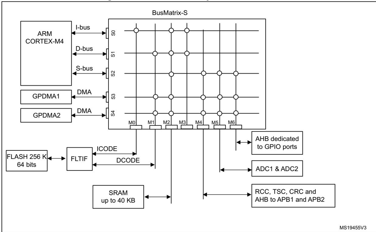
This diagram illustrates the system architecture for the STM32F302xB/C series. At the center is the BusMatrix-S , which acts as a switching matrix for the system buses. On the left, the ARM CORTEX-M4 processor is connected via its I-bus (Instruction), D-bus (Data), and S-bus (System) to the matrix. Below the processor, GPDMA1 and GPDMA2 are connected via DMA signals. The matrix has seven output ports labeled M0 through M6 . M0 connects to the FLASH 256 K 64 bits through an FLTIF (Flash Interface) using ICODE and DCODE signals. M1 connects to SRAM up to 40 KB . M2 connects to a block containing ADC1 & ADC2 . M3 connects to a block containing RCC, TSC, CRC and AHB to APB1 and APB2 . M4 connects to AHB dedicated to GPIO ports . M5 and M6 are also connected to the AHB dedicated to GPIO ports block. The matrix itself is a grid with switches at the intersections of the seven horizontal lines (labeled S0 to S6 on the left) and the seven vertical lines (labeled M0 to M6 at the bottom).
MS19455V3
Figure 2. STM32F302x6/8 system architecture
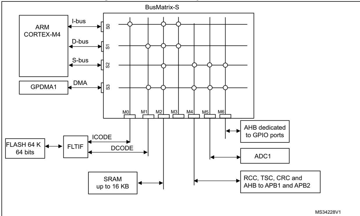
This diagram illustrates the system architecture for the STM32F302x6/8 series. It features the same BusMatrix-S as Figure 1. The ARM CORTEX-M4 processor is connected via its I-bus , D-bus , and S-bus . GPDMA1 is connected via DMA . The matrix output ports are: M0 to FLASH 64 K 64 bits through FLTIF ( ICODE , DCODE ); M1 to SRAM up to 16 KB ; M2 to ADC1 ; M3 to RCC, TSC, CRC and AHB to APB1 and APB2 ; M4 to AHB dedicated to GPIO ports ; and M5 and M6 also to AHB dedicated to GPIO ports . The matrix grid has seven horizontal lines (labeled S0 to S6 ) and seven vertical lines (labeled M0 to M6 ).
MS34228V1
Figure 3. STM32F302xD/E system architecture
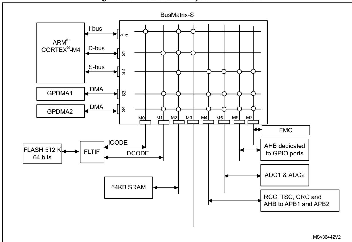
The diagram illustrates the system architecture of the STM32F302xD/E microcontroller. At the center is the BusMatrix-S , a matrix with 8 masters (M0-M7) and 8 slaves (S0-S7). The masters are connected to the matrix as follows:
- ARM® CORTEX®-M4 connects via its I-bus (to S0), D-bus (to S1), and S-bus (to S2).
- GPDMA1 and GPDMA2 both connect via their DMA interfaces (to S3 and S4).
- S0 (I-bus) connects to FLASH 512 K 64 bits via ICODE and FLTIF .
- S1 (D-bus) connects to FLASH 512 K 64 bits via DCODE and FLTIF .
- S2 (S-bus) connects to 64KB SRAM , ADC1 & ADC2 , and RCC, TSC, CRC and AHB to APB1 and APB2 .
- S3, S4 (DMA-bus) connect to 64KB SRAM , ADC1 & ADC2 , RCC, TSC, CRC and AHB to APB1 and APB2 , and AHB dedicated to GPIO ports .
- S5 connects to FMC .
- S6 connects to AHB dedicated to GPIO ports .
- S7 connects to RCC, TSC, CRC and AHB to APB1 and APB2 .
3.1.1 S0: I-bus
This bus connects the Instruction bus of the Cortex®-M4 core to the BusMatrix. This bus is used by the core to fetch instructions. The targets of this bus are the internal Flash memory and the SRAM.
3.1.2 S1: D-bus
This bus connects the DCode bus (literal load and debug access) of the Cortex®-M4 core to the BusMatrix. The targets of this bus are the internal Flash memory and the SRAM.
3.1.3 S2: S-bus
This bus connects the system bus of the Cortex®-M4 core to the BusMatrix. This bus is used to access data located in the peripheral or SRAM area. The targets of this bus are the SRAM, the AHB to APB1/APB2 bridges, the AHB IO port and the 2 ADCs.
3.1.4 S3, S4: DMA-bus
This bus connects the AHB master interface of the DMA to the BusMatrix which manages the access of different Masters to Flash, SRAM and peripherals.
3.1.5 BusMatrix
The BusMatrix manages the access arbitration between Masters. The arbitration uses a Round Robin algorithm. The BusMatrix is composed of five masters (CPU AHB, System bus, DCode bus, ICode bus, DMA1/2 bus) and seven slaves (FLITF, SRAM, AHB2GPIO and AHB2APB1/2 bridges, and ADCs).
AHB/APB bridges
The two AHB/APB bridges provide full synchronous connections between the AHB and the two APB buses. APB1 is limited to 36 MHz, APB2 operates at full speed (72 MHz).
Refer to Section 2.2.2: Memory map and register boundary addresses on page 48 for the address mapping of the peripherals connected to this bridge.
After each device reset, all peripheral clocks are disabled (except for the SRAM and FLITF). Before using a peripheral user has to enable its clock in the RCC_AHBENR, RCC_APB2ENR or RCC_APB1ENR register.
When a 16- or 8-bit access is performed on an APB register, the access is transformed into a 32-bit access: the bridge duplicates the 16- or 8-bit data to feed the 32-bit vector.
3.2 Memory organization
3.2.1 Introduction
Program memory, data memory, registers and I/O ports are organized within the same linear 4-Gbyte address space.
The bytes are coded in memory in Little Endian format. The lowest numbered byte in a word is considered the word's least significant byte and the highest numbered byte the most significant.
The addressable memory space is divided into eight main blocks, of 512 Mbytes each.
3.2.2 Memory map and register boundary addresses
Refer to the device datasheet for a comprehensive diagram of the memory map.
The following table gives the boundary addresses of the peripherals available in the devices.
Table 2. STM32F302xB/C peripheral register boundary addresses (1)
| Bus | Boundary address | Size (bytes) | Peripheral | Peripheral register map |
|---|---|---|---|---|
| AHB3 | 0x5000 0000 - 0x5000 03FF | 1 K | ADC1 - ADC2 | Section 15.7 on page 393 |
| - | 0x4800 1800 - 0x4FFF FFFF | ~132 M | Reserved | - |
| AHB2 | 0x4800 1400 - 0x4800 17FF | 1 K | GPIOF | Section 10.4.12 on page 173 |
| 0x4800 1000 - 0x4800 13FF | 1 K | GPIOE | ||
| 0x4800 0C00 - 0x4800 0FFF | 1 K | GPIO D | ||
| 0x4800 0800 - 0x4800 0BFF | 1 K | GPIOC | ||
| 0x4800 0400 - 0x4800 07FF | 1 K | GPIOB | ||
| 0x4800 0000 - 0x4800 03FF | 1 K | GPIOA | ||
| - | 0x4002 4400 - 0x47FF FFFF | ~128 M | Reserved | |
| AHB1 | 0x4002 4000 - 0x4002 43FF | 1 K | TSC | Section 19.6.11 on page 457 |
| 0x4002 3400 - 0x4002 3FFF | 3 K | Reserved | - | |
| 0x4002 3000 - 0x4002 33FF | 1 K | CRC | Section 6.4.6 on page 91 | |
| 0x4002 2400 - 0x4002 2FFF | 3 K | Reserved | - | |
| 0x4002 2000 - 0x4002 23FF | 1 K | Flash interface | Section 4.6 on page 80 | |
| 0x4002 1400 - 0x4002 1FFF | 3 K | Reserved | - | |
| 0x4002 1000 - 0x4002 13FF | 1 K | RCC | Section 9.4.14 on page 155 | |
| 0x4002 0800 - 0x4002 0FFF | 2 K | Reserved | - | |
| 0x4002 0400 - 0x4002 07FF | 1 K | DMA2 | Section 12.6.7 on page 208 | |
| 0x4002 0000 - 0x4002 03FF | 1 K | DMA1 | ||
| - | 0x4001 8000 - 0x4001 FFFF | 32 K | Reserved | - |
| Bus | Boundary address | Size (bytes) | Peripheral | Peripheral register map |
|---|---|---|---|---|
| APB2 | 0x4001 4C00 - 0x4001 7FFF | 13 K | Reserved | - |
| 0x4001 4800 - 0x4001 4BFF | 1 K | TIM17 | Section 22.6.18 on page 701 | |
| 0x4001 4400 - 0x4001 47FF | 1 K | TIM16 | ||
| 0x4001 4000 - 0x4001 43FF | 1 K | TIM15 | Section 22.5.19 on page 681 | |
| 0x4001 3C00 - 0x4001 3FFF | 1 K | Reserved | - | |
| 0x4001 3800 - 0x4001 3BFF | 1 K | USART1 | Section 25.7.12 on page 708 | |
| 0x4001 3400 - 0x4001 37FF | 1 K | Reserved | - | |
| 0x4001 3000 - 0x4001 33FF | 1 K | SPI1 | Section 30.9.10 on page 967 | |
| 0x4001 2C00 - 0x4001 2FFF | 1 K | TIM1 | Section 20.4.27 on page 551 | |
| 0x4001 0800 - 0x4001 2BFF | 8 K | Reserved | - | |
| 0x4001 0400 - 0x4001 07FF | 1 K | EXTI | Section 13.3.13 on page 229 | |
| 0x4001 0000 - 0x4001 03FF | 1 K | SYSCFG + COMP + OPAMP | Section 11.1.7 on page 184
, Section 17.5.5 on page 425 , Section 18.4.3 on page 439 | |
| - | 0x4000 9C00 - 0x4000 FFFF | 25 K | Reserved | - |
| Bus | Boundary address | Size (bytes) | Peripheral | Peripheral register map |
|---|---|---|---|---|
| APB1 | 0x4000 7800 - 0x4000 9BFF | 9 K | Reserved | - |
| 0x4000 7400 - 0x4000 77FF | 1 K | DAC1 | Section 16.9.8 on page 410 | |
| 0x4000 7000 - 0x4000 73FF | 1 K | PWR | Section 8.4.3 on page 115 | |
| 0x4000 6C00 - 0x4000 6FFF | 1 K | Reserved | - | |
| 0x4000 6800 - 0x4000 6BFF | 1 K | Reserved | - | |
| 0x4000 6400 - 0x4000 67FF | 1 K | bxCAN | Section 31.9.5 on page 1006 | |
| 0x4000 6000 - 0x4000 63FF | 1 K | USB SRAM | Section 32.6.3 on page 1041 | |
| 0x4000 5C00 - 0x4000 5FFF | 1 K | USB device FS | ||
| 0x4000 5800 - 0x4000 5BFF | 1 K | I2C2 | Section 28.7.12 on page 842 | |
| 0x4000 5400 - 0x4000 57FF | 1 K | I2C1 | ||
| 0x4000 5000 - 0x4000 53FF | 1 K | UART5 | Section 25.7.12 on page 708 | |
| 0x4000 4C00 - 0x4000 4FFF | 1 K | UART4 | ||
| 0x4000 4800 - 0x4000 4BFF | 1 K | USART3 | ||
| 0x4000 4400 - 0x4000 47FF | 1 K | USART2 | ||
| 0x4000 3400 - 0x4000 43FF | 4 K | Reserved | ||
| 0x4000 3000 - 0x4000 33FF | 1 K | IWDG | Section 26.4.6 on page 731 | |
| 0x4000 2C00 - 0x4000 2FFF | 1 K | WWDG | Section 25.5.4 on page 721 | |
| 0x4000 2800 - 0x4000 2BFF | 1 K | RTC | Section 27.6.20 on page 773 | |
| 0x4000 1400 - 0x4000 27FF | 5 K | Reserved | - | |
| 0x4000 1000 - 0x4000 13FF | 1 K | TIM6 | Section 23.4.9 on page 715 | |
| 0x4000 0C00 - 0x4000 0FFF | 1 K | Reserved | - | |
| 0x4000 0800 - 0x4000 0BFF | 1 K | TIM4 | Section 21.4.22 on page 622 | |
| 0x4000 0400 - 0x4000 07FF | 1 K | TIM3 | ||
| 0x4000 0000 - 0x4000 03FF | 1 K | TIM2 | ||
| - | 0x2000 A000 - 3FFF FFFF | ~512 M | Reserved | - |
| - | 0x2000 0000 - 0x2000 9FFF | 40 K | SRAM | - |
| - | 0x1FFF F800 - 0x1FFF FFFF | 2 K | Option bytes | - |
| - | 0x1FFF D800 - 0x1FFF F7FF | 8 K | System memory | - |
| - | 0x0804 0000 - 0x1FFF D7FF | ~384 M | Reserved | - |
| - | 0x0800 0000 - 0x0803 FFFF | 256 K | Main Flash memory | - |
| - | 0x0004 0000 - 0x07FF FFFF | ~128 M | Reserved | - |
| - | 0x0000 000 - 0x0003 FFFF | 256 K | Main Flash memory, system memory or SRAM depending on BOOT configuration | - |
1. The gray color is used for reserved Flash memory addresses.
Table 3. STM32F302x/D/E peripheral register boundary addresses (1)| Bus | Boundary address | Size (bytes) | Peripheral | Peripheral register map |
|---|---|---|---|---|
| AHB4 | 0xA000 0000 - 0xA000 0FFF | 4 K | FMC control registers | Section 14 on page 231 |
| 0x8000 0000 - 0x9FFF FFFF | 512 M | FMC Banks 3 and 4 | ||
| 0x6000 0000 - 0x7FFF FFFF | 512 M | FMC Banks 1 and 2 | ||
| AHB3 | 0x5000 0000 - 0x5000 03FF | 1 K | ADC1 - ADC2 | Section 15.7 on page 393 |
| - | 0x4800 2000 - 0x4FFF FFFF | ~132 M | Reserved | - |
| AHB2 | 0x4800 1C00 - 0x4800 1FFF | 1 K | GPIOH | Section 10.4.12 on page 173 |
| 0x4800 1800 - 0x4800 1BFF | 1 K | GPIOG | ||
| 0x4800 1400 - 0x4800 17FF | 1 K | GPIOF | ||
| 0x4800 1000 - 0x4800 13FF | 1 K | GPIOE | ||
| 0x4800 0C00 - 0x4800 0FFF | 1 K | GPIO D | ||
| 0x4800 0800 - 0x4800 0BFF | 1 K | GPIOC | ||
| 0x4800 0400 - 0x4800 07FF | 1 K | GPIOB | ||
| 0x4800 0000 - 0x4800 03FF | 1 K | GPIOA | ||
| - | 0x4002 4400 - 0x47FF FFFF | ~128 M | Reserved | |
| AHB1 | 0x4002 4000 - 0x4002 43FF | 1 K | TSC | Section 19.6.11 on page 457 |
| 0x4002 3400 - 0x4002 3FFF | 3 K | Reserved | - | |
| 0x4002 3000 - 0x4002 33FF | 1 K | CRC | Section 6.4.6 on page 91 | |
| 0x4002 2400 - 0x4002 2FFF | 3 K | Reserved | - | |
| 0x4002 2000 - 0x4002 23FF | 1 K | Flash interface | Section 4.6 on page 80 | |
| 0x4002 1400 - 0x4002 1FFF | 3 K | Reserved | - | |
| 0x4002 1000 - 0x4002 13FF | 1 K | RCC | Section 9.4.14 on page 155 | |
| 0x4002 0800 - 0x4002 0FFF | 2 K | Reserved | - | |
| 0x4002 0400 - 0x4002 07FF | 1 K | DMA2 | Section 12.6.7 on page 208 | |
| 0x4002 0000 - 0x4002 03FF | 1 K | DMA1 | ||
| - | 0x4001 8000 - 0x4001 FFFF | 32 K | Reserved | - |
| Bus | Boundary address | Size (bytes) | Peripheral | Peripheral register map |
|---|---|---|---|---|
| APB2 | 0x4001 4C00 - 0x4001 7FFF | 13 K | Reserved | - |
| 0x4001 4800 - 0x4001 4BFF | 1 K | TIM17 | Section 22.6.18 on page 701 | |
| 0x4001 4400 - 0x4001 47FF | 1 K | TIM16 | ||
| 0x4001 4000 - 0x4001 43FF | 1 K | TIM15 | Section 22.5.19 on page 681 | |
| 0x4001 3C00 - 0x4001 3FFF | 1 K | SPI4 | Section 30.9.10 on page 967 | |
| 0x4001 3800 - 0x4001 3BFF | 1 K | USART1 | Section 25.7.12 on page 708 | |
| 0x4001 3400 - 0x4001 37FF | 1 K | Reserved | - | |
| 0x4001 3000 - 0x4001 33FF | 1 K | SPI1 | Section 30.9.10 on page 967 | |
| 0x4001 2C00 - 0x4001 2FFF | 1 K | TIM1 | Section 20.4.27 on page 551 | |
| 0x4001 0800 - 0x4001 2BFF | 8 K | Reserved | - | |
| 0x4001 0400 - 0x4001 07FF | 1 K | EXTI | Section 13.3.13 on page 229 | |
| 0x4001 0000 - 0x4001 03FF | 1 K | SYSCFG + COMP + OPAMP | Section 11.1.7 on page 184
, Section 17.5.5 on page 425 , Section 18.4.3 on page 439 | |
| - | 0x4000 9C00 - 0x4000 FFFF | 25 K | Reserved | - |
| Bus | Boundary address | Size (bytes) | Peripheral | Peripheral register map |
|---|---|---|---|---|
| APB1 | 0x4000 7800 - 0x4000 9BFF | 9 K | Reserved | - |
| 0x4000 7400 - 0x4000 77FF | 1 K | DAC1 | Section 16.9.8 on page 410 | |
| 0x4000 7000 - 0x4000 73FF | 1 K | PWR | Section 8.4.3 on page 115 | |
| 0x4000 6C00 - 0x4000 6FFF | 1 K | Reserved | - | |
| 0x4000 6800 - 0x4000 6BFF | 1 K | Reserved | - | |
| 0x4000 6400 - 0x4000 67FF | 1 K | bxCAN | Section 31.9.5 on page 1006 | |
| 0x4000 6000 - 0x4000 63FF | 1 K | USB/CAN SRAM | Section 32.6.3 on page 1041 | |
| 0x4000 5C00 - 0x4000 5FFF | 1 K | USB device FS | ||
| 0x4000 5800 - 0x4000 5BFF | 1 K | I2C2 | Section 28.7.12 on page 842 | |
| 0x4000 5400 - 0x4000 57FF | 1 K | I2C1 | ||
| 0x4000 5000 - 0x4000 53FF | 1 K | UART5 | Section 25.7.12 on page 708 | |
| 0x4000 4C00 - 0x4000 4FFF | 1 K | UART4 | ||
| 0x4000 4800 - 0x4000 4BFF | 1 K | USART3 | ||
| 0x4000 4400 - 0x4000 47FF | 1 K | USART2 | ||
| 0x4000 3400 - 0x4000 43FF | 4 K | Reserved | ||
| 0x4000 3000 - 0x4000 33FF | 1 K | IWDG | Section 26.4.6 on page 731 | |
| 0x4000 2C00 - 0x4000 2FFF | 1 K | WWDG | Section 25.5.4 on page 721 | |
| 0x4000 2800 - 0x4000 2BFF | 1 K | RTC | Section 27.6.20 on page 773 | |
| 0x4000 1400 - 0x4000 27FF | 5 K | Reserved | - | |
| 0x4000 1000 - 0x4000 13FF | 1 K | TIM6 | Section 23.4.9 on page 715 | |
| 0x4000 0C00 - 0x4000 0FFF | 1 K | Reserved | - | |
| 0x4000 0800 - 0x4000 0BFF | 1 K | TIM4 | Section 21.4.22 on page 622 | |
| 0x4000 0400 - 0x4000 07FF | 1 K | TIM3 | ||
| 0x4000 0000 - 0x4000 03FF | 1 K | TIM2 | ||
| - | 0x2000 A000 - 3FFF FFFF | ~512 M | Reserved | - |
| - | 0x2000 0000 - 0x2000 FFFF | 64 K | SRAM | - |
| - | 0x1FFF F800 - 0x1FFF FFFF | 2 K | Option bytes | - |
| - | 0x1FFF D800 - 0x1FFF F7FF | 8 K | System memory | - |
| - | 0x0804 0000 - 0x1FFF D7FF | ~384 M | Reserved | - |
| - | 0x0800 0000 - 0x0807 FFFF | 512 K | Main Flash memory | - |
| - | 0x0004 0000 - 0x07FF FFFF | ~128 M | Reserved | - |
| - | 0x0000 000 - 0x0007 FFFF | 512 K | Main Flash memory, system memory or SRAM depending on BOOT configuration | - |
1. The gray color is used for reserved Flash memory addresses.
Table 4. STM32F302x6/x8 peripheral register boundary addresses (1)| Bus | Boundary address | Size (bytes) | Peripheral | Peripheral register map |
|---|---|---|---|---|
| AHB3 | 0x5000 0000 - 0x5000 03FF | 1 K | ADC1 | Section 15.7 on page 393 |
| - | 0x4800 1800 - 0x4FFF FFFF | ~132 M | Reserved | - |
| AHB2 | 0x4800 1400 - 0x4800 17FF | 1 K | GPIOF | Section 10.4.12 on page 173 |
| 0x4800 1000 - 0x4800 13FF | 1 K | Reserved | - | |
| 0x4800 0C00 - 0x4800 0FFF | 1 K | GPIOE | Section 10.4.12 on page 173 | |
| 0x4800 0800 - 0x4800 0BFF | 1 K | GPIOC | ||
| 0x4800 0400 - 0x4800 07FF | 1 K | GPIOB | ||
| 0x4800 0000 - 0x4800 03FF | 1 K | GPIOA | ||
| - | 0x4002 4400 - 0x47FF FFFF | ~128 M | Reserved | |
| AHB1 | 0x4002 4000 - 0x4002 43FF | 1 K | TSC | Section 19.6.11 on page 457 |
| 0x4002 3400 - 0x4002 3FFF | 3 K | Reserved | - | |
| 0x4002 3000 - 0x4002 33FF | 1 K | CRC | Section 6.4.6 on page 91 | |
| 0x4002 2400 - 0x4002 2FFF | 3 K | Reserved | - | |
| 0x4002 2000 - 0x4002 23FF | 1 K | Flash interface | Section 4.6 on page 80 | |
| 0x4002 1400 - 0x4002 1FFF | 3 K | Reserved | - | |
| 0x4002 1000 - 0x4002 13FF | 1 K | RCC | Section 9.4.14 on page 155 | |
| 0x4002 0400 - 0x4002 0FFF | 3 K | Reserved | - | |
| 0x4002 0000 - 0x4002 03FF | 1 K | DMA1 | Section 12.6.7 on page 208 | |
| - | 0x4001 8000 - 0x4001 FFFF | 32 K | Reserved | - |
| APB2 | 0x4001 4C00 - 0x4001 7FFF | 13 K | Reserved | - |
| 0x4001 4800 - 0x4001 4BFF | 1 K | TIM17 | Section 22.6.18 on page 701 | |
| 0x4001 4400 - 0x4001 47FF | 1 K | TIM16 | ||
| 0x4001 4000 - 0x4001 43FF | 1 K | TIM15 | Section 22.5.19 on page 681 | |
| 0x4001 3C00 - 0x4001 3FFF | 1 K | Reserved | - | |
| 0x4001 3800 - 0x4001 3BFF | 1 K | USART1 | Section 25.7.12 on page 708 | |
| 0x4001 2C00 - 0x4001 2FFF | 1 K | TIM1 | Section 20.4.27 on page 551 | |
| 0x4001 0800 - 0x4001 2BFF | 8 K | Reserved | - | |
| 0x4001 0400 - 0x4001 07FF | 1 K | EXTI | Section 13.3.13 on page 229 | |
| 0x4001 0000 - 0x4001 03FF | 1 K | SYSCFG + COMP + OPAMP | Section 11.1.7 on page 184
, Section 17.5.5 on page 425 , Section 18.4.3 on page 439 | |
| - | 0x4000 9C00 - 0x4000 FFFF | 25 K | Reserved | - |
| Bus | Boundary address | Size (bytes) | Peripheral | Peripheral register map |
|---|---|---|---|---|
| APB1 | 0x4000 7C00 - 0x4000 9BFF | 8 K | Reserved | - |
| 0x4000 7800 - 0x4000 7BFF | 1 K | I2C3 | Section 28.7.12 on page 842 | |
| 0x4000 7400 - 0x4000 77FF | 1 K | DAC1 | Section 16.9.8 on page 410 | |
| 0x4000 7000 - 0x4000 73FF | 1 K | PWR | Section 8.4.3 on page 115 | |
| 0x4000 6800 - 0x4000 6FFF | 2 K | Reserved | - | |
| 0x4000 6400 - 0x4000 67FF | 1 K | bxCAN | Section 31.9.5 on page 1006 | |
| 0x4000 6000 - 0x4000 63FF | 1 K | USB/CAN SRAM | Section 32.6.3 on page 1041 | |
| 0x4000 5C00 - 0x4000 5FFF | 1 K | USB device FS | ||
| 0x4000 5800 - 0x4000 5BFF | 1 K | I2C2 | Section 28.7.12 on page 842 | |
| 0x4000 5400 - 0x4000 57FF | 1 K | I2C1 | ||
| 0x4000 4C00 - 0x4000 53FF | 2 K | Reserved | - | |
| 0x4000 4800 - 0x4000 4BFF | 1 K | USART3 | Section 25.7.12 on page 708 | |
| 0x4000 4400 - 0x4000 47FF | 1 K | USART2 | ||
| 0x4000 4000 - 0x4000 43FF | 1 K | I2S3ext | Section 30.9.10 on page 967 | |
| 0x4000 3C00 - 0x4000 3FFF | 1 K | SPI3/I2S3 | ||
| 0x4000 3800 - 0x4000 3BFF | 1 K | SPI2/I2S2 | ||
| 0x4000 3400 - 0x4000 37FF | 1 K | I2S2ext | ||
| 0x4000 3000 - 0x4000 33FF | 1 K | IWDG | Section 26.4.6 on page 731 | |
| 0x4000 2C00 - 0x4000 2FFF | 1 K | WWDG | Section 25.5.4 on page 721 | |
| 0x4000 2800 - 0x4000 2BFF | 1 K | RTC | Section 27.6.20 on page 773 | |
| 0x4000 1400 - 0x4000 27FF | 5 K | Reserved | - | |
| 0x4000 1000 - 0x4000 13FF | 1 K | TIM6 | Section 23.4.9 on page 715 | |
| 0x4000 0400 - 0x4000 0FFF | 3 K | Reserved | - | |
| 0x4000 0000 - 0x4000 03FF | 1 K | TIM2 | Section 21.4.22 on page 622 | |
| - | 0x2000 4000 - 3FFF FFFF | ~512 M | Reserved | - |
| - | 0x2000 0000 - 0x2000 3FFF | 16 K | SRAM | - |
| - | 0x1FFF F800 - 0x1FFF FFFF | 2 K | Option bytes | - |
| - | 0x1FFF D800 - 0x1FFF F7FF | 8 K | System memory | - |
| - | 0x0801 0000 - 0x1FFF D7FF | ~384 M | Reserved | - |
| - | 0x0800 0000 - 0x0800 FFFF | 64 K | Main Flash memory | - |
| - | 0x0001 0000 - 0x07FF FFFF | ~128 M | Reserved | - |
| - | 0x0000 000 - 0x0000 FFFF | 64 K | Main Flash memory, system memory or SRAM depending on BOOT configuration | - |
1. The gray color is used for reserved Flash memory addresses.
3.3 Embedded SRAM
STM32F302xB/C devices feature up to 40 Kbytes of static SRAM. It can be accessed as bytes, halfwords (16 bits) or full words (32 bits). It can be addressed at maximum system clock frequency without wait states and can be accessed by both CPU and DMA.
STM32F302x6/8 devices feature only up to 16 Kbytes of static SRAM.
STM32F302xD/E devices feature up to 64 Kbytes of static SRAM.
3.3.1 Parity check
On the STM32F302xD/E devices, for the 40-Kbyte SRAM, a parity check is implemented only on the first 16 Kbytes.
On the STM32F302xD/E devices, the parity check is implemented on the first 32 Kbytes of SRAM. On the STM32F302x6/x8 the SRAM parity check is not supported. The SRAM parity check is disabled by default. It is enabled by the user, when needed, using an option bit.
The data bus width of the SRAM supporting the parity check is 36 bits because 4 bits are available for parity check (1 bit per byte) in order to increase memory robustness, as required for instance by Class B or SIL norms.
The parity bits are computed on data and address and stored when writing into the SRAM. Then, they are automatically checked when reading. If one bit fails, an NMI is generated if the SRAM parity check is enabled. The same error can also be linked to the Break input of TIMER 1, 8, 15, 16 and 17, by setting the SRAM_PARITY_LOCK control bit in the SYSCFG configuration register 2 (SYSCFG_CFGR2). In case of parity error, the SRAM Parity Error flag (SRAM_PEF) is set in SYSCFG_CFGR2. For more details, refer to SYSCFG_CFGR2.
The BYP_ADD_PAR bit in SYSCFG_CFGR2 can be used to prevent an unwanted parity error to occur when the user programs a code in the RAM at address 0x2XXXXXXX (address in the address range 0x20000000-0x20002000) and then executes the code from RAM at boot (RAM is remapped at address 0x00).
3.4 Flash memory overview
The Flash memory is composed of two distinct physical areas:
- • The main Flash memory block. It contains the application program and user data if necessary.
- • The information block. It is composed of two parts:
- – Option bytes for hardware and memory protection user configuration
- – System memory which contains the proprietary boot loader code. Refer to Section 4: Embedded Flash memory for more details.
Flash memory instructions and data access are performed through the AHB bus. The prefetch block is used for instruction fetches through the ICode bus. Arbitration is performed in the Flash memory interface, and priority is given to data access on the DCode bus. It also implements the logic necessary to carry out the Flash memory operations (Program/Erase) controlled through the Flash registers.
3.5 Boot configuration
In the STM32F302xx, three different boot modes can be selected through the BOOT0 pin and nBOOT1 bit in the user option byte, as shown in the following table:
Table 5. Boot modes
| Boot mode selection | Boot mode | Aliasings | |
|---|---|---|---|
| nBOOT1 | BOOT0 | - | - |
| x | 0 | Main Flash memory | Main Flash memory selected as boot area |
| 1 | 1 | System memory | System memory selected as boot area |
| 0 | 1 | Embedded SRAM | Embedded SRAM (on the DCode bus) selected as boot area |
The values on both BOOT0 pin and nBOOT1 bit are latched on the 4th rising edge of SYSCLK after a reset.
It is up to the user to set the nBOOT1 and BOOT0 to select the required boot mode. The BOOT0 pin and nBOOT1 bit are also resampled when exiting from Standby mode. Consequently they must be kept in the required Boot mode configuration in Standby mode. After this startup delay has elapsed, the CPU fetches the top-of-stack value from address 0x0000 0000, then starts code execution from the boot memory at 0x0000 0004. Depending on the selected boot mode, main Flash memory, system memory or SRAM is accessible as follows:
- • Boot from main Flash memory: the main Flash memory is aliased in the boot memory space (0x0000 0000), but still accessible from its original memory space (0x0800 0000). In other words, the Flash memory contents can be accessed starting from address 0x0000 0000 or 0x0800 0000.
- • Boot from system memory: the system memory is aliased in the boot memory space (0x0000 0000), but still accessible from its original memory space (0x1FFF D800).
- • Boot from the embedded SRAM: the SRAM is aliased in the boot memory space (0x0000 0000), but it is still accessible from its original memory space (0x2000 0000).
3.5.1 Embedded boot loader
The embedded boot loader is located in the system memory, programmed by ST during production. It is used to reprogram the Flash memory through the following peripherals:
- • USART1(PA9/PA10), USART2(PD5/PD6) or USB(PA11/PA12) on STM32F302xB/C devices
- • USART1(PA9/PA10), USART2(PA2/PA3) or USB(PA11/PA12) on STM32F302x6/8 and STM32F302xD/E devices.