23. Universal synchronous/asynchronous receiver transmitter (USART/UART)
23.1 Introduction
The universal synchronous asynchronous receiver transmitter (USART) offers a flexible means of Full-duplex data exchange with external equipment requiring an industry standard NRZ asynchronous serial data format. The USART offers a very wide range of baud rates using a programmable baud rate generator.
It supports synchronous one-way communication and Half-duplex Single-wire communication, as well as multiprocessor communications. It also supports Modem operations (CTS/RTS).
High speed data communication is possible by using the DMA (direct memory access) for multibuffer configuration.
23.2 USART main features
- • Full-duplex asynchronous communications
- • NRZ standard format (mark/space)
- • Configurable oversampling method by 16 or 8 to give flexibility between speed and clock tolerance
- • A common programmable transmit and receive baud rate of up to 6 Mbit/s when the clock frequency is 48 MHz and oversampling is by 8
- • Convenient baud rate programming
- • Auto baud rate detection
- • Programmable data word length (8 or 9 bits)
- • Programmable data order with MSB-first or LSB-first shifting
- • Configurable stop bits (1 or 2 stop bits)
- • Synchronous mode and clock output for synchronous communications
- • Single-wire Half-duplex communications
- • Continuous communications using DMA
- • Received/transmitted bytes are buffered in reserved SRAM using centralized DMA
- • Separate enable bits for transmitter and receiver
- • Separate signal polarity control for transmission and reception
- • Swappable Tx/Rx pin configuration
- • Hardware flow control for modem and RS-485 transceiver
- • Communication control/error detection flags
- • Parity control:
- – Transmits parity bit
- – Checks parity of received data byte
- • Fourteen interrupt sources with flags
- • Multiprocessor communications
The USART enters Mute mode if the address does not match. - • Wake-up from Mute mode (by idle line detection or address mark detection)
23.3 USART implementation
Table 86. STM32F0x0 USART features (1)
| USART modes/ features | STM32F030x4, STM32F030x6 | STM32F030x8 | STM32F070x6 | STM32F070xB | STM32F030xC | |||||||
|---|---|---|---|---|---|---|---|---|---|---|---|---|
| USART1 | USART1 | USART2 | USART1 | USART2 | USART1/ USART2 | USART3 | USART4 | USART1/ USART2/ USART3 | USART4 | USART5 | USART6 | |
| Hardware flow control for modem | X | X | X | X | X | X | X | X | X | X | - | - |
| Continuous communication using DMA | X | X | X | X | X | X | X | - | X | X | X | X |
| Multiprocessor communication | X | X | X | X | X | X | X | X | X | X | X | X |
| Synchronous mode | X | X | X | X | X | X | X | X | X | X | X | - |
| Smartcard mode | - | - | - | - | - | - | - | - | - | - | - | - |
| Single-wire Half-duplex communication | X | X | X | X | X | X | X | X | X | X | X | X |
| IrDA SIR ENDEC block | - | - | - | - | - | - | - | - | - | - | - | - |
| LIN mode | - | - | - | - | - | - | - | - | - | - | - | - |
| Dual clock domain and wake-up from Stop mode | - | - | - | - | - | - | - | - | - | - | - | - |
| Receiver timeout interrupt | X | X | - | X | - | X | - | - | X | - | - | - |
| Modbus communication | - | - | - | - | - | - | - | - | - | - | - | - |
| Auto baud rate detection (supported modes) | 2 | 2 | - | 4 | - | 4 | - | - | 4 | - | - | - |
| Driver Enable | X | X | X | X | X | X | X | X | X | X | X | - |
| USART data length | 8 and 9 bits | 7 (2) , 8 and 9 bits | ||||||||||
1. X = supported.
2. In 7-bit data length mode, Smartcard mode, LIN master mode and Auto baud rate (0x7F and 0x55 frames) detection are not supported.
23.4 USART functional description
Any USART bidirectional communication requires a minimum of two pins: Receive data In (RX) and Transmit data Out (TX):
- • RX: Receive data Input.
This is the serial data input. Oversampling techniques are used for data recovery by discriminating between valid incoming data and noise.
- • TX: Transmit data Output.
When the transmitter is disabled, the output pin returns to its I/O port configuration. When the transmitter is enabled and nothing is to be transmitted, the TX pin is at high level. In Single-wire, this I/O is used to transmit and receive the data.
Serial data are transmitted and received through these pins in normal USART mode. The frames are comprised of:
- • An Idle Line prior to transmission or reception
- • A start bit
- • A data word (8 or 9 bits) least significant bit first
- • 1, 2 stop bits indicating that the frame is complete
- • The USART interface uses a baud rate generator
- • A status register (USART_ISR)
- • Receive and transmit data registers (USART_RDR, USART_TDR)
- • A baud rate register (USART_BRR)
Refer to Section 23.7: USART registers on page 620 for the definitions of each bit.
The following pin is required to interface in synchronous mode:
- • CK: Clock output. This pin outputs the transmitter data clock for synchronous transmission corresponding to SPI master mode (no clock pulses on start bit and stop bit, and a software option to send a clock pulse on the last data bit). In parallel, data can be received synchronously on RX. This can be used to control peripherals that have shift registers. The clock phase and polarity are software programmable.
The following pins are required in RS232 Hardware flow control mode:
- • CTS: Clear To Send blocks the data transmission at the end of the current transfer (when high)
- • RTS: Request to send indicates that the USART is ready to receive data (when low).
The following pin is required in RS485 Hardware control mode:
- • DE: Driver Enable activates the transmission mode of the external transceiver.
Note: DE and RTS share the same pin.
Figure 230. USART block diagram
![Figure 230. USART block diagram. This is a detailed block diagram of the USART/UART peripheral. At the top, a 'CPU or DMA' block is shown interacting with the USART. It has 'Read' and 'Write' paths. The 'Read' path goes through a 'Transmit shift register' and a 'Transmit data register (TDR)' to 'PRDATA'. The 'Write' path goes through 'PWDATA' to a 'Receive shift register' and a 'Receive data register (RDR)'. Below these registers are several control and configuration registers: 'USART_CR3 register', 'USART_CR2 register', 'USART_CR1 register', and 'USART_GTPR register' (with 'GT' and 'PSC' fields). A 'Hardware flow controller' block on the left takes 'RTS / DE' and 'CTS' signals and connects to the 'Transmit control' and 'Receiver control' blocks. The 'Transmit control' block is connected to 'USART_CR1 register' and 'USART_interrupt control'. The 'Receiver control' block is connected to 'USART_CR1 register', 'USART_ISR register', and 'Receiver clock'. A 'Conventional baud rate generator' block at the bottom right contains 'USART_BRR register', 'Transmitter rate controller', 'BRR[15:0]', and 'Receiver rate controller'. It is controlled by 'TE' and 'RE' signals and provides a 'Transmitter clock' to the 'USART' blocks. The 'Transmitter clock' is derived from 'fPCLK' and a divider '/USARTDIV or 2/USARTDIV (depending on the oversampling mode) (Note 1)'. A 'CK' (clock) signal is shown on the right side, connected to 'CK control' which is influenced by 'USART_CR2 register' and 'USART_GTPR register'.](/RM0360-STM32F030x4-x6-x8-xC-070x6-xB/e2a38c69472356a3407bb79de8cf3a15_img.jpg)
- 1. For details on coding USARTDIV in the USART_BRR register, refer to Section 23.4.4: USART baud rate generation .
23.4.1 USART character description
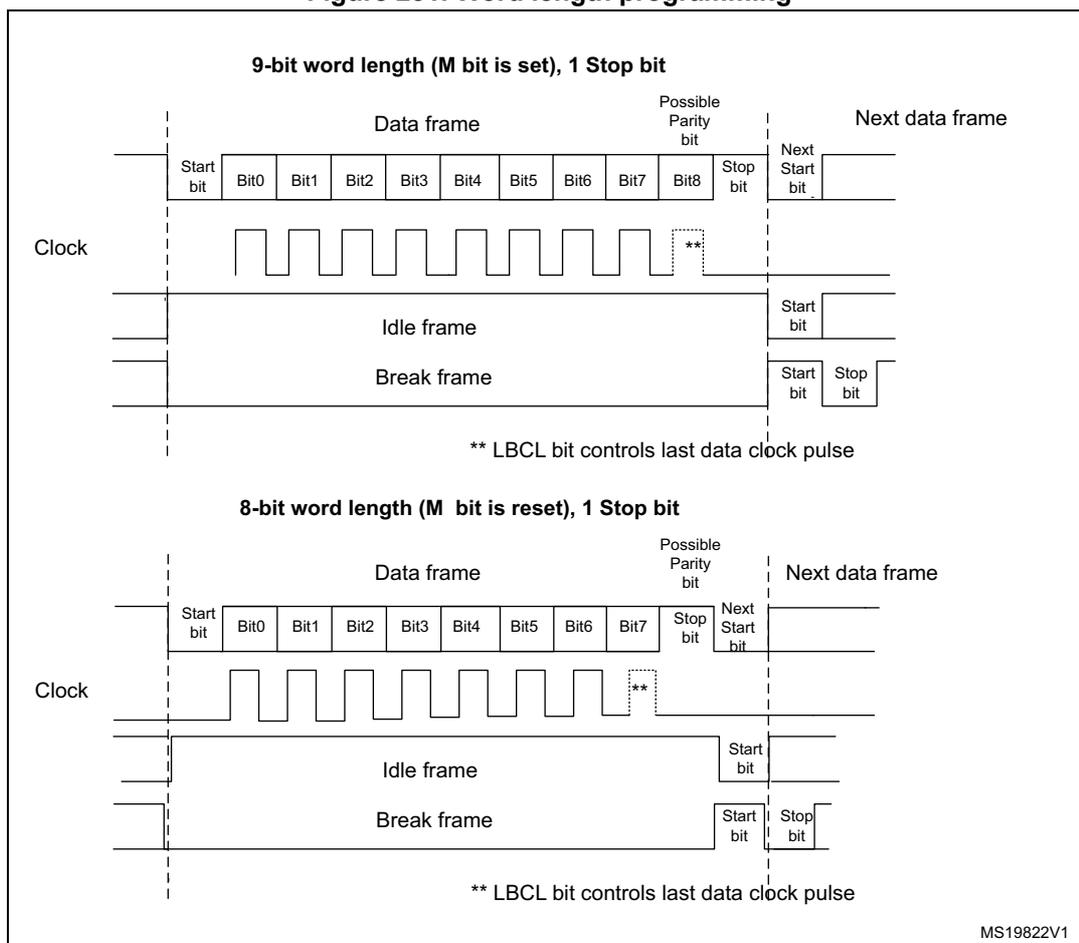
The word length can be selected as being either 8 or 9 bits by programming the M bit (M0: bit 12) in the USART_CR1 register (see Figure 231 ).
- • 8-bit character length: M0 = 0
- • 9-bit character length: M0 = 1
By default, the signal (TX or RX) is in low state during the start bit. It is in high state during the stop bit.
These values can be inverted, separately for each signal, through polarity configuration control.
An Idle character is interpreted as an entire frame of “1”s (the number of “1”s includes the number of stop bits).
A Break character is interpreted on receiving “0”s for a frame period. At the end of the break frame, the transmitter inserts 2 stop bits.
Transmission and reception are driven by a common baud rate generator, the clock for each is generated when the enable bit is set respectively for the transmitter and receiver.
The details of each block is given below.
Figure 231. Word length programming
23.4.2 USART transmitter
The transmitter can send data words of either 8 or 9 bits depending on the M bit status. The Transmit Enable bit (TE) must be set in order to activate the transmitter function. The data in the transmit shift register is output on the TX pin and the corresponding clock pulses are output on the CK pin.
Character transmission
During an USART transmission, data shifts out least significant bit first (default configuration) on the TX pin. In this mode, the USART_TDR register consists of a buffer (TDR) between the internal bus and the transmit shift register (see Figure 230).
Every character is preceded by a start bit which is a logic level low for one bit period. The character is terminated by a configurable number of stop bits.
The following stop bits are supported by USART: 1 and 2 stop bits.
Note: The TE bit must be set before writing the data to be transmitted to the USART_TDR.
The TE bit should not be reset during transmission of data. Resetting the TE bit during the transmission will corrupt the data on the TX pin as the baud rate counters will get frozen. The current data being transmitted is lost.
An idle frame is sent after the TE bit is enabled.
Configurable stop bits
The number of stop bits to be transmitted with every character can be programmed in Control register 2, bits 13,12.
- • 1 stop bit: This is the default value of number of stop bits.
- • 2 stop bits: This is supported by normal USART, Single-wire and Modem modes.
An idle frame transmission will include the stop bits.
A break transmission will be 10 low bits (when M0= 0) or 11 low bits (when M0= 1) followed by 2 stop bits (see Figure 232 ). It is not possible to transmit long breaks (break of length greater than 10/11 low bits).
Figure 232. Configurable stop bits
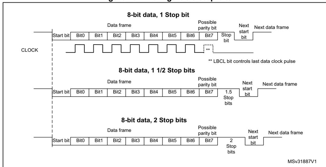
The diagram shows three data frame structures for 8-bit data transmission, each with a different number of stop bits. A CLOCK signal is shown below the frames. The first frame shows 1 stop bit. The second frame shows 1.5 stop bits. The third frame shows 2 stop bits. A note indicates that the LBCL bit controls the last data clock pulse.
8-bit data, 1 Stop bit
Data frame: Start bit | Bit0 | Bit1 | Bit2 | Bit3 | Bit4 | Bit5 | Bit6 | Bit7 | Possible parity bit | Stop bit | Next start bit | Next data frame
8-bit data, 1 1/2 Stop bits
Data frame: Start bit | Bit0 | Bit1 | Bit2 | Bit3 | Bit4 | Bit5 | Bit6 | Bit7 | Possible parity bit | 1.5 Stop bits | Next start bit | Next data frame
8-bit data, 2 Stop bits
Data frame: Start bit | Bit0 | Bit1 | Bit2 | Bit3 | Bit4 | Bit5 | Bit6 | Bit7 | Possible parity bit | 2 Stop bits | Next start bit | Next data frame
** LBCL bit controls last data clock pulse
MSv31887V1
Character transmission procedure
- 1. Program the M bit in USART_CR1 to define the word length.
- 2. Select the desired baud rate using the USART_BRR register.
- 3. Program the number of stop bits in USART_CR2.
- 4. Enable the USART by writing the UE bit in USART_CR1 register to 1.
- 5. Select DMA enable (DMAT) in USART_CR3 if multibuffer communication is to take place. Configure the DMA register as explained in multibuffer communication.
- 6. Set the TE bit in USART_CR1 to send an idle frame as first transmission.
- 7. Write the data to send in the USART_TDR register (this clears the TXE bit). Repeat this for each data to be transmitted in case of single buffer.
- 8. After writing the last data into the USART_TDR register, wait until TC=1. This indicates that the transmission of the last frame is complete. This is required for instance when the USART is disabled or enters the Halt mode to avoid corrupting the last transmission.
For code example, refer to A.15.1: USART transmitter configuration .
Single byte communication
Clearing the TXE bit is always performed by a write to the transmit data register.
The TXE bit is set by hardware and it indicates:
- • The data has been moved from the USART_TDR register to the shift register and the data transmission has started.
- • The USART_TDR register is empty.
- • The next data can be written in the USART_TDR register without overwriting the previous data.
For code example, refer to A.15.2: USART transmit byte .
This flag generates an interrupt if the TXEIE bit is set.
When a transmission is taking place, a write instruction to the USART_TDR register stores the data in the TDR register; next, the data is copied in the shift register at the end of the currently ongoing transmission.
When no transmission is taking place, a write instruction to the USART_TDR register places the data in the shift register, the data transmission starts, and the TXE bit is set.
If a frame is transmitted (after the stop bit) and the TXE bit is set, the TC bit goes high. An interrupt is generated if the TCIE bit is set in the USART_CR1 register.
After writing the last data in the USART_TDR register, it is mandatory to wait for TC=1 before disabling the USART or causing the microcontroller to enter the low-power mode (see Figure 233: TC/TXE behavior when transmitting ).
Figure 233. TC/TXE behavior when transmitting
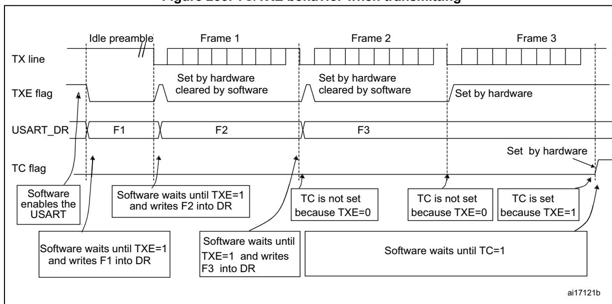
The diagram illustrates the timing and flag behavior for transmitting three frames (Frame 1, Frame 2, Frame 3) after an idle preamble. The horizontal axis represents time, and the vertical axis shows the state of the TX line, TXE flag, USART_DR register, and TC flag.
- TX line: Shows the idle preamble followed by the transmission of Frame 1, Frame 2, and Frame 3.
- TXE flag:
- Initially low.
- Set by hardware when the first character (F1) is written to USART_DR.
- Cleared by software when the next character (F2) is written.
- Set by hardware when F2 is written.
- Cleared by software when F3 is written.
- Set by hardware when F3 is written.
- Remains set until the transmission is complete.
- USART_DR: Shows the data characters F1, F2, and F3 being written sequentially.
- TC flag:
- Initially low.
- Not set when F1 or F2 are written because TXE=0.
- Set by hardware when TXE=1 (after F3 is written).
Software sequence:
- Software enables the USART.
- Software waits until TXE=1 and writes F1 into DR.
- Software waits until TXE=1 and writes F2 into DR.
- TC is not set because TXE=0.
- Software waits until TXE=1 and writes F3 into DR.
- TC is not set because TXE=0.
- Software waits until TC=1.
ai17121b
For code example, refer to A.15.3: USART transfer complete .
Break characters
Setting the SBKRQ bit transmits a break character. The break frame length depends on the M bit (see Figure 231 ).
If a '1' is written to the SBKRQ bit, a break character is sent on the TX line after completing the current character transmission. The SBKF bit is set by the write operation and it is reset by hardware when the break character is completed (during the stop bits after the break character). The USART inserts a logic 1 signal (STOP) for the duration of 2 bits at the end of the break frame to guarantee the recognition of the start bit of the next frame.
In the case the application needs to send the break character following all previously inserted data, including the ones not yet transmitted, the software should wait for the TXE flag assertion before setting the SBKRQ bit.
Idle characters
Setting the TE bit drives the USART to send an idle frame before the first data frame.
23.4.3 USART receiver
The USART can receive data words of either 8 or 9 bits depending on the M bit in the USART_CR1 register.
Start bit detection
The start bit detection sequence is the same when oversampling by 16 or by 8.
In the USART, the start bit is detected when a specific sequence of samples is recognized. This sequence is: 1 1 1 0 X 0 X 0X 0X 0 X 0X 0.
Figure 234. Start bit detection when oversampling by 16 or 8
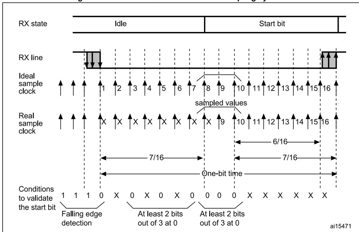
The diagram illustrates the start bit detection process when oversampling by 16 or 8. The RX state transitions from Idle to Start bit. The RX line shows a falling edge for the start bit. The Ideal sample clock has 16 samples per bit, while the Real sample clock has 8 samples per bit. Sampling points are indicated by arrows. The 'sampled values' are taken at the 3rd, 5th, 7th, 8th, 9th, and 10th clock cycles. The 'Conditions to validate the start bit' are shown as a sequence of 1s and 0s: 1 1 1 0 X 0 X 0 X 0 0 0 X X X X X X. The first four samples (1 1 1 0) are used for 'Falling edge detection'. The next three samples (X 0 X) and the following three samples (0 X 0) are used to check if 'At least 2 bits out of 3 at 0'. The remaining samples (0 0 0 X X X X X X) are ignored. Time intervals of 7/16 and 6/16 bit times are marked between sampling points.
Note: If the sequence is not complete, the start bit detection aborts and the receiver returns to the idle state (no flag is set), where it waits for a falling edge.
The start bit is confirmed (RXNE flag set, interrupt generated if RXNEIE=1) if the 3 sampled bits are at 0 (first sampling on the 3rd, 5th and 7th bits finds the 3 bits at 0 and second sampling on the 8th, 9th and 10th bits also finds the 3 bits at 0).
The start bit is validated (RXNE flag set, interrupt generated if RXNEIE=1) but the NF noise flag is set if,
- for both samplings, 2 out of the 3 sampled bits are at 0 (sampling on the 3rd, 5th and 7th bits and sampling on the 8th, 9th and 10th bits)
- or
- for one of the samplings (sampling on the 3rd, 5th and 7th bits or sampling on the 8th, 9th and 10th bits), 2 out of the 3 bits are found at 0.
If neither conditions a. or b. are met, the start detection aborts and the receiver returns to the idle state (no flag is set).
Character reception
During an USART reception, data shifts in least significant bit first (default configuration) through the RX pin. In this mode, the USART_RDR register consists of a buffer (RDR) between the internal bus and the receive shift register.
Character reception procedure
- 1. Program the M bit in USART_CR1 to define the word length.
- 2. Select the desired baud rate using the baud rate register USART_BRR
- 3. Program the number of stop bits in USART_CR2.
- 4. Enable the USART by writing the UE bit in USART_CR1 register to 1.
- 5. Select DMA enable (DMAR) in USART_CR3 if multibuffer communication is to take place. Configure the DMA register as explained in multibuffer communication.
- 6. Set the RE bit USART_CR1. This enables the receiver which begins searching for a start bit.
For code example, refer to A.15.4: USART receiver configuration .
When a character is received:
- • The RXNE bit is set to indicate that the content of the shift register is transferred to the RDR. In other words, data has been received and can be read (as well as its associated error flags).
- • An interrupt is generated if the RXNEIE bit is set.
- • The error flags can be set if a frame error, noise or an overrun error has been detected during reception. PE flag can also be set with RXNE.
- • In multibuffer, RXNE is set after every byte received and is cleared by the DMA read of the Receive data Register.
- • In single buffer mode, clearing the RXNE bit is performed by a software read to the USART_RDR register. The RXNE flag can also be cleared by writing 1 to the RXFRQ in the USART_RQR register. The RXNE bit must be cleared before the end of the reception of the next character to avoid an overrun error.
For code example, refer to A.15.5: USART receive byte .
Break character
When a break character is received, the USART handles it as a framing error.
Idle character
When an idle frame is detected, there is the same procedure as for a received data character plus an interrupt if the IDLEIE bit is set.
Overrun error
An overrun error occurs when a character is received when RXNE has not been reset. Data can not be transferred from the shift register to the RDR register until the RXNE bit is cleared.
The RXNE flag is set after every byte received. An overrun error occurs if RXNE flag is set when the next data is received or the previous DMA request has not been serviced. When an overrun error occurs:
- • The ORE bit is set.
- • The RDR content will not be lost. The previous data is available when a read to USART_RDR is performed.
- • The shift register are overwritten. After that point, any data received during overrun is lost.
- • An interrupt is generated if either the RXNEIE bit is set or EIE bit is set.
- • The ORE bit is reset by setting the ORECF bit in the ICR register.
Note: The ORE bit, when set, indicates that at least 1 datum has been lost. There are two possibilities:
- - if RXNE=1, then the last valid data is stored in the receive register RDR and can be read,
- - if RXNE=0, then it means that the last valid data has already been read and thus there is nothing to be read in the RDR. This case can occur when the last valid data is read in the RDR at the same time as the new (and lost) data is received.
Selecting the clock source and the proper oversampling method
The choice of the clock source is done through the Clock Control system (see Section Reset and clock control (RCC))). The clock source must be chosen before enabling the USART (by setting the UE bit).
The choice of the clock source must be done according to two criteria:
- • Possible use of the USART in low-power mode
- • Communication speed.
The clock source frequency is \( f_{CK} \) .
The communication speed range (specially the maximum communication speed) is also determined by the clock source.
The receiver implements different user-configurable oversampling techniques for data recovery by discriminating between valid incoming data and noise. This allows a trade-off between the maximum communication speed and noise/clock inaccuracy immunity.
The oversampling method can be selected by programming the OVER8 bit in the USART_CR1 register and can be either 16 or 8 times the baud rate clock ( Figure 235 and Figure 236 ).
Depending on the application:
- • Select oversampling by 8 (OVER8=1) to achieve higher speed (up to \( f_{CK}/8 \) ). In this case the maximum receiver tolerance to clock deviation is reduced (refer to Section 23.4.5: Tolerance of the USART receiver to clock deviation on page 606 )
- • Select oversampling by 16 (OVER8=0) to increase the tolerance of the receiver to clock deviations. In this case, the maximum speed is limited to maximum \( f_{CK}/16 \) where \( f_{CK} \) is the clock source frequency.
Programming the ONEBIT bit in the USART_CR3 register selects the method used to evaluate the logic level. There are two options:
- • The majority vote of the three samples in the center of the received bit. In this case, when the 3 samples used for the majority vote are not equal, the NF bit is set
- • A single sample in the center of the received bit
Depending on the application:
- – select the three samples' majority vote method (ONEBIT=0) when operating in a noisy environment and reject the data when a noise is detected (refer to Figure 87 ) because this indicates that a glitch occurred during the sampling.
- – select the single sample method (ONEBIT=1) when the line is noise-free to increase the receiver's tolerance to clock deviations (see Section 23.4.5: Tolerance of the USART receiver to clock deviation on page 606 ). In this case the NF bit will never be set.
When noise is detected in a frame:
- • The NF bit is set at the rising edge of the RXNE bit.
- • The invalid data is transferred from the Shift register to the USART_RDR register.
- • No interrupt is generated in case of single byte communication. However this bit rises at the same time as the RXNE bit which itself generates an interrupt. In case of multibuffer communication an interrupt is issued if the EIE bit is set in the USART_CR3 register.
The NF bit is reset by setting NFCF bit in ICR register.
Figure 235. Data sampling when oversampling by 16
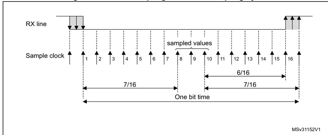
Figure 236. Data sampling when oversampling by 8
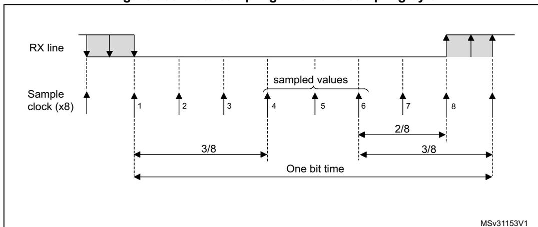
Table 87. Noise detection from sampled data
| Sampled value | NE status | Received bit value |
|---|---|---|
| 000 | 0 | 0 |
| 001 | 1 | 0 |
| 010 | 1 | 0 |
| 011 | 1 | 1 |
| 100 | 1 | 0 |
| 101 | 1 | 1 |
| 110 | 1 | 1 |
| 111 | 0 | 1 |
Framing error
A framing error is detected when the stop bit is not recognized on reception at the expected time, following either a de-synchronization or excessive noise.
When the framing error is detected:
- • The FE bit is set by hardware
- • The invalid data is transferred from the Shift register to the USART_RDR register.
- • No interrupt is generated in case of single byte communication. However this bit rises at the same time as the RXNE bit which itself generates an interrupt. In case of multibuffer communication an interrupt is issued if the EIE bit is set in the USART_CR3 register.
The FE bit is reset by writing 1 to the FECF in the USART_ICR register.
Configurable stop bits during reception
The number of stop bits to be received can be configured through the control bits of Control Register 2 - it can be either 1 or 2 in normal mode.
- • 1 stop bit: Sampling for 1 stop Bit is done on the 8th, 9th and 10th samples.
- • 2 stop bits: Sampling for 2 stop bits is done on the 8th, 9th and 10th samples of the first stop bit. If a framing error is detected during the first stop bit the framing error flag is set. The second stop bit is not checked for framing error. The RXNE flag is set at the end of the first stop bit.
23.4.4 USART baud rate generation
The baud rate for the receiver and transmitter (Rx and Tx) are both set to the same value as programmed in the USART_BRR register.
Equation 1: Baud rate for standard USART (SPI mode included) (OVER8 = 0 or 1)
In case of oversampling by 16, the equation is:
In case of oversampling by 8, the equation is:
USARTDIV is an unsigned fixed point number that is coded on the USART_BRR register.
- • When OVER8 = 0, BRR = USARTDIV.
- • When OVER8 = 1
- – BRR[2:0] = USARTDIV[3:0] shifted 1 bit to the right.
- – BRR[3] must be kept cleared.
- – BRR[15:4] = USARTDIV[15:4]
Note: The baud counters are updated to the new value in the baud registers after a write operation to USART_BRR. Hence the baud rate register value should not be changed during communication.
In case of oversampling by 16 or 8, USARTDIV must be greater than or equal to 16d.
How to derive USARTDIV from USART_BRR register values
Example 1
To obtain 9600 baud with \( f_{CK} = 8 \) MHz.
- • In case of oversampling by 16:
- – USARTDIV = 8 000 000/9600
- – BRR = USARTDIV = 0d833 = 0x341
- • In case of oversampling by 8:
- – USARTDIV = 2 * 8 000 000/9600
- – USARTDIV = 1666,66 (0d1667 = 0x683)
- – BRR[3:0] = 0x3 >> 1 = 0x1
- – BRR = 0x681
To obtain 921.6 kbaud with \( f_{CK} = 48 \) MHz.
- In case of oversampling by 16:
\( USARTDIV = 48\,000\,000/921\,600 \)
\( BRR = USARTDIV = 52d = 34h \) - In case of oversampling by 8:
\( USARTDIV = 2 * 48\,000\,000/921\,600 \)
\( USARTDIV = 104 (104d = 68h) \)
\( BRR[3:0] = USARTDIV[3:0] \gg 1 = 8h \gg 1 = 4h \)
\( BRR = 0x64 \)
Table 88. Error calculation for programmed baud rates at \( f_{CK} = 48 \) MHz in both cases of oversampling by 16 or by 8 (1)
| Baud rate | Oversampling by 16 (OVER8 = 0) | Oversampling by 8 (OVER8 = 1) | |||||
|---|---|---|---|---|---|---|---|
| S.No | Desired | Actual | BRR | % Error = (Calculated - Desired)B.Rate/ Desired B.Rate | Actual | BRR | % Error |
| 2 | 2.4 KBps | 2.4 KBps | 0x4E20 | 0 | 2.4 KBps | 0x9C40 | 0 |
| 3 | 9.6 KBps | 9.6 KBps | 0x1388 | 0 | 9.6 KBps | 0x2710 | 0 |
| 4 | 19.2 KBps | 19.2 KBps | 0x9C4 | 0 | 19.2 KBps | 0x1384 | 0 |
| 5 | 38.4 KBps | 38.4 KBps | 0x4E2 | 0 | 38.4 KBps | 0x9C2 | 0 |
| 6 | 57.6 KBps | 57.62 KBps | 0x341 | 0.03 | 57.59 KBps | 0x681 | 0.02 |
| 7 | 115.2 KBps | 115.11 KBps | 0x1A1 | 0.08 | 115.25 KBps | 0x340 | 0.04 |
| 8 | 230.4 KBps | 230.76 KBps | 0xD0 | 0.16 | 230.21 KBps | 0x1A0 | 0.08 |
| 9 | 460.8 KBps | 461.54 KBps | 0x68 | 0.16 | 461.54 KBps | 0xD0 | 0.16 |
| 10 | 921.6 KBps | 923.07 KBps | 0x34 | 0.16 | 923.07 KBps | 0x64 | 0.16 |
| 11 | 2 MBps | 2 MBps | 0x18 | 0 | 2 MBps | 0x30 | 0 |
| 12 | 3 MBps | 3 MBps | 0x10 | 0 | 3 MBps | 0x20 | 0 |
| 13 | 4 MBps | N.A | N.A | N.A | 4 MBps | 0x14 | 0 |
| 14 | 5 MBps | N.A | N.A | N.A | 5052.63 KBps | 0x11 | 1.05 |
| 15 | 6 MBps | N.A | N.A | N.A | 6 MBps | 0x10 | 0 |
1. The lower the CPU clock the lower the accuracy for a particular baud rate. The upper limit of the achievable baud rate can be fixed with these data.
23.4.5 Tolerance of the USART receiver to clock deviation
The asynchronous receiver of the USART works correctly only if the total clock system deviation is less than the tolerance of the USART receiver. The causes which contribute to the total deviation are:
- • DTRA: Deviation due to the transmitter error (which also includes the deviation of the transmitter's local oscillator)
- • DQUANT: Error due to the baud rate quantization of the receiver
- • DREC: Deviation of the receiver's local oscillator
- • DTCL: Deviation due to the transmission line (generally due to the transceivers which can introduce an asymmetry between the low-to-high transition timing and the high-to-low transition timing)
The USART receiver can receive data correctly at up to the maximum tolerated deviation specified in Table 89 and Table 90 depending on the following choices:
- • 10- or 11-bit character length defined by the M bit in the USART_CR1 register
- • Oversampling by 8 or 16 defined by the OVER8 bit in the USART_CR1 register
- • Bits BRR[3:0] of USART_BRR register are equal to or different from 0000.
- • Use of 1 bit or 3 bits to sample the data, depending on the value of the ONEBIT bit in the USART_CR3 register.
Table 89. Tolerance of the USART receiver when BRR [3:0] = 0000
| M bit | OVER8 bit = 0 | OVER8 bit = 1 | ||
|---|---|---|---|---|
| ONEBIT=0 | ONEBIT=1 | ONEBIT=0 | ONEBIT=1 | |
| 0 | 3.75% | 4.375% | 2.50% | 3.75% |
| 1 | 3.41% | 3.97% | 2.27% | 3.41% |
Table 90. Tolerance of the USART receiver when BRR [3:0] is different from 0000
| M bit | OVER8 bit = 0 | OVER8 bit = 1 | ||
|---|---|---|---|---|
| ONEBIT=0 | ONEBIT=1 | ONEBIT=0 | ONEBIT=1 | |
| 0 | 3.33% | 3.88% | 2% | 3% |
| 1 | 3.03% | 3.53% | 1.82% | 2.73% |
Note: The data specified in Table 89 , and Table 90 may slightly differ in the special case when the received frames contain some Idle frames of exactly 10-bit durations when M = 0 (11-bit durations when M = 1).
23.4.6 USART auto baud rate detection
The USART is able to detect and automatically set the USART_BRR register value based on the reception of one character. Automatic baud rate detection is useful under two circumstances:
- • The communication speed of the system is not known in advance
- • The system is using a relatively low accuracy clock source and this mechanism allows the correct baud rate to be obtained without measuring the clock deviation.
The clock source frequency must be compatible with the expected communication speed (Oversampling by 16 must be selected for a baud rate between \( f_{CK}/65535 \) and \( f_{CK}/16 \) ).
Before activating the auto baud rate detection, the auto baud rate detection mode must be chosen. There are various modes based on different character patterns.
They can be chosen through the ABRMOD[1:0] field in the USART_CR2 register. In these auto baud rate modes, the baud rate is measured several times during the synchronization data reception and each measurement is compared to the previous one.
These modes are:
- • Mode 0: Any character starting with a bit at 1. In this case the USART measures the duration of the Start bit (falling edge to rising edge).
- • Mode 1: Any character starting with a 10xx bit pattern. In this case, the USART measures the duration of the Start and of the 1st data bit. The measurement is done falling edge to falling edge, ensuring better accuracy in the case of slow signal slopes.
In parallel, another check is performed for each intermediate transition of RX line. An error is generated if the transitions on RX are not sufficiently synchronized with the receiver (the receiver being based on the baud rate calculated on bit 0).
Prior to activating auto baud rate detection, the USART_BRR register must be initialized by writing a non-zero baud rate value.
The automatic baud rate detection is activated by setting the ABREN bit in the USART_CR2 register. The USART will then wait for the first character on the RX line. The auto baud rate operation completion is indicated by the setting of the ABRF flag in the USART_ISR register. If the line is noisy, the correct baud rate detection cannot be guaranteed. In this case the BRR value may be corrupted and the ABRE error flag is set. This also happens if the communication speed is not compatible with the automatic baud rate detection range (bit duration not between 16 and 65536 clock periods (oversampling by 16) and not between 8 and 65536 clock periods (oversampling by 8)).
The RXNE interrupt will signal the end of the operation.
At any later time, the auto baud rate detection may be relaunched by resetting the ABRF flag (by writing a 0).
Note: If the USART is disabled (UE=0) during an auto baud rate operation, the BRR value may be corrupted.
23.4.7 Multiprocessor communication using USART
In multiprocessor communication, the following bits are to be kept cleared:
- • LINEN bit in the USART_CR2 register,
- • HDSEL, IREN and SCEN bits in the USART_CR3 register.
It is possible to perform multiprocessor communication with the USART (with several USARTs connected in a network). For instance one of the USARTs can be the master, its TX output connected to the RX inputs of the other USARTs. The others are slaves, their respective TX outputs are logically ANDed together and connected to the RX input of the master.
In multiprocessor configurations it is often desirable that only the intended message recipient should actively receive the full message contents, thus reducing redundant USART service overhead for all non addressed receivers.
The non addressed devices may be placed in mute mode by means of the muting function. In order to use the mute mode feature, the MME bit must be set in the USART_CR1 register.
In mute mode:
- • None of the reception status bits can be set.
- • All the receive interrupts are inhibited.
- • The RWU bit in USART_ISR register is set to 1. RWU can be controlled automatically by hardware or by software, through the MMRQ bit in the USART_RQR register, under certain conditions.
The USART can enter or exit from mute mode using one of two methods, depending on the WAKE bit in the USART_CR1 register:
- • Idle Line detection if the WAKE bit is reset,
- • Address Mark detection if the WAKE bit is set.
Idle line detection (WAKE=0)
The USART enters mute mode when the MMRQ bit is written to 1 and the RWU is automatically set. It wakes up when an Idle frame is detected. Then the RWU bit is cleared by hardware but the IDLE bit is not set in the USART_ISR register. An example of mute mode behavior using Idle line detection is given in Figure 237.
Figure 237. Mute mode using Idle line detection
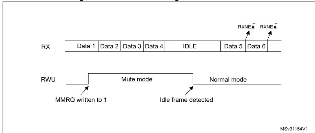
The diagram illustrates the behavior of the USART in mute mode using Idle line detection. The RX line shows a sequence of data frames: Data 1, Data 2, Data 3, Data 4, followed by an IDLE state, then Data 5 and Data 6. The RWU line shows a transition from Normal mode to Mute mode when the MMRQ bit is written to 1. The USART exits mute mode when an Idle frame is detected. RXNE flags are shown for Data 5 and Data 6, indicating that reception is disabled during the IDLE state.
MSv31154V1
Note: If the MMRQ is set while the IDLE character has already elapsed, mute mode will not be entered (RWU is not set).
If the USART is activated while the line is IDLE, the idle state is detected after the duration of one IDLE frame (not only after the reception of one character frame).
4-bit/7-bit address mark detection (WAKE=1)
In this mode, bytes are recognized as addresses if their MSB is a '1' otherwise they are considered as data. In an address byte, the address of the targeted receiver is put in the 4 or 7 LSBs. The choice of 7 or 4-bit address detection is done using the ADDM7 bit. This 4-bit/7-bit word is compared by the receiver with its own address which is programmed in the ADD bits in the USART_CR2 register.
Note: In 7-bit and 9-bit data modes, address detection is done on 6-bit and 8-bit addresses (ADD[5:0] and ADD[7:0]) respectively.
The USART enters mute mode when an address character is received which does not match its programmed address. In this case, the RWU bit is set by hardware. The RXNE flag is not set for this address byte and no interrupt or DMA request is issued when the USART enters mute mode.
The USART also enters mute mode when the MMRQ bit is written to 1. The RWU bit is also automatically set in this case.
The USART exits from mute mode when an address character is received which matches the programmed address. Then the RWU bit is cleared and subsequent bytes are received normally. The RXNE bit is set for the address character since the RWU bit has been cleared.
An example of mute mode behavior using address mark detection is given in Figure 238 .
Figure 238. Mute mode using address mark detection
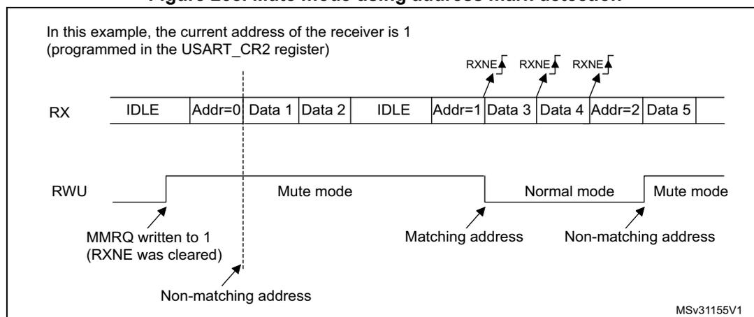
In this example, the current address of the receiver is 1 (programmed in the USART_CR2 register)
The diagram illustrates the RX and RWU signals over time. The RX signal shows a sequence of IDLE, Addr=0, Data 1, Data 2, IDLE, Addr=1, Data 3, Data 4, Addr=2, Data 5. The RWU signal shows transitions between Mute mode and Normal mode. Mute mode is entered when Addr=0 (non-matching) or Addr=2 (non-matching) is received, and exited when Addr=1 (matching) is received. RXNE flags are set for Addr=1, Data 3, and Data 4.
Key events shown:
- MMRQ written to 1 (RXNE was cleared): The initial transition to Mute mode.
- Non-matching address (Addr=0): The first address byte received, which does not match the programmed address 1, causing the RWU bit to be set and the USART to enter Mute mode.
- Matching address (Addr=1): The second address byte received, which matches the programmed address 1, causing the RWU bit to be cleared and the USART to enter Normal mode. The RXNE flag is set for this address character.
- Non-matching address (Addr=2): The third address byte received, which does not match the programmed address 1, causing the RWU bit to be set and the USART to enter Mute mode again.
MSv31155V1
23.4.8 USART parity control
Parity control (generation of parity bit in transmission and parity checking in reception) can be enabled by setting the PCE bit in the USART_CR1 register. Depending on the frame length defined by the M bit, the possible USART frame formats are as listed in Table 91 .
Table 91. Frame formats
| M bit | PCE bit | USART frame (1) |
|---|---|---|
| 0 | 0 | | SB | 8-bit data | STB | |
| 0 | 1 | | SB | 7-bit data | PB | STB | |
| 1 | 0 | | SB | 9-bit data | STB | |
| 1 | 1 | | SB | 8-bit data | PB | STB | |
1. Legends: SB: start bit, STB: stop bit, PB: parity bit. In the data register, the PB is always taking the MSB position (8th or 7th, depending on the M bits value).
Even parity
The parity bit is calculated to obtain an even number of “1s” inside the frame of the 7 or 8 LSB bits (depending on M bit value) and the parity bit.
As an example, if data=00110101, and 4 bits are set, then the parity bit is 0 if even parity is selected ( PS bit in USART_CR1 = 0).
Odd parity
The parity bit is calculated to obtain an odd number of “1s” inside the frame made of the 7 or 8 LSB bits (depending on M bit value) and the parity bit.
As an example, if data=00110101 and 4 bits set, then the parity bit is 1 if odd parity is selected ( PS bit in USART_CR1 = 1).
Parity checking in reception
If the parity check fails, the PE flag is set in the USART_ISR register and an interrupt is generated if PEIE is set in the USART_CR1 register. The PE flag is cleared by software writing 1 to the PECF in the USART_ICR register.
Parity generation in transmission
If the PCE bit is set in USART_CR1 , then the MSB bit of the data written in the data register is transmitted but is changed by the parity bit (even number of “1s” if even parity is selected ( PS =0) or an odd number of “1s” if odd parity is selected ( PS =1)).
For code example, refer to A.15.6: USART synchronous mode .
23.4.9 USART synchronous mode
The synchronous mode is selected by writing the CLKEN bit in the USART_CR2 register to 1. In synchronous mode, the following bits must be kept cleared:
- • SCEN , HDSEL and IREN bits in the USART_CR3 register.
In this mode, the USART can be used to control bidirectional synchronous serial communications in master mode. The CK pin is the output of the USART transmitter clock.
No clock pulses are sent to the CK pin during start bit and stop bit. Depending on the state of the LBCL bit in the USART_CR2 register, clock pulses are, or are not, generated during the last valid data bit (address mark). The CPOL bit in the USART_CR2 register is used to select the clock polarity, and the CPHA bit in the USART_CR2 register is used to select the phase of the external clock (see Figure 239 , Figure 240 and Figure 241 ).
During the Idle state, preamble and send break, the external CK clock is not activated.
In synchronous mode the USART transmitter works exactly like in asynchronous mode. But as CK is synchronized with TX (according to CPOL and CPHA), the data on TX is synchronous.
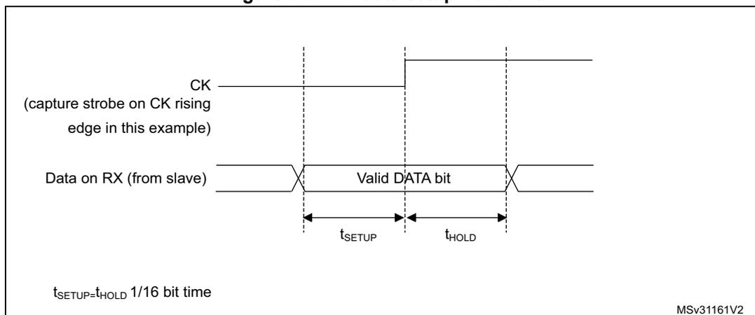
In this mode the USART receiver works in a different manner compared to the asynchronous mode. If RE=1, the data is sampled on CK (rising or falling edge, depending on CPOL and CPHA), without any oversampling. A setup and a hold time must be respected (which depends on the baud rate: 1/16 bit duration).
Note:
The CK pin works in conjunction with the TX pin. Thus, the clock is provided only if the transmitter is enabled (TE=1) and data is being transmitted (the data register USART_TDR written). This means that it is not possible to receive synchronous data without transmitting data.
The LBCL, CPOL and CPHA bits have to be selected when the USART is disabled (UE=0) to ensure that the clock pulses function correctly.
For code example, refer to A.15.6: USART synchronous mode .
Figure 239. USART example of synchronous transmission
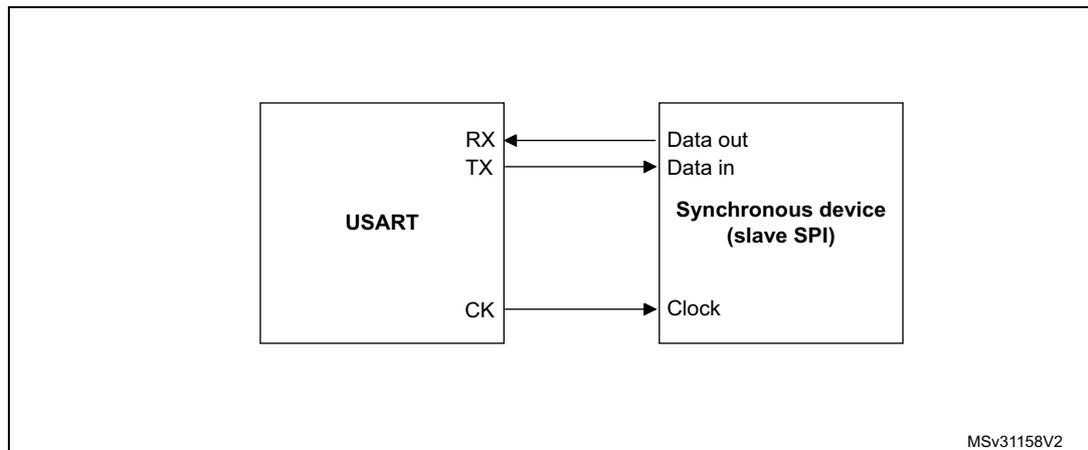
The diagram illustrates the connections for synchronous transmission. On the left is a block labeled 'USART' with three pins: 'RX', 'TX', and 'CK'. On the right is a block labeled 'Synchronous device (slave SPI)' with three corresponding pins: 'Data out / Data in' and 'Clock'. Arrows indicate the signal flow: 'TX' from USART to 'Data in' of the slave device, 'Data out' from the slave device to 'RX' of the USART, and 'CK' from USART to 'Clock' of the slave device. The identifier 'MSv31158V2' is located in the bottom right corner of the diagram area.
Figure 240. USART data clock timing diagram (M=0)
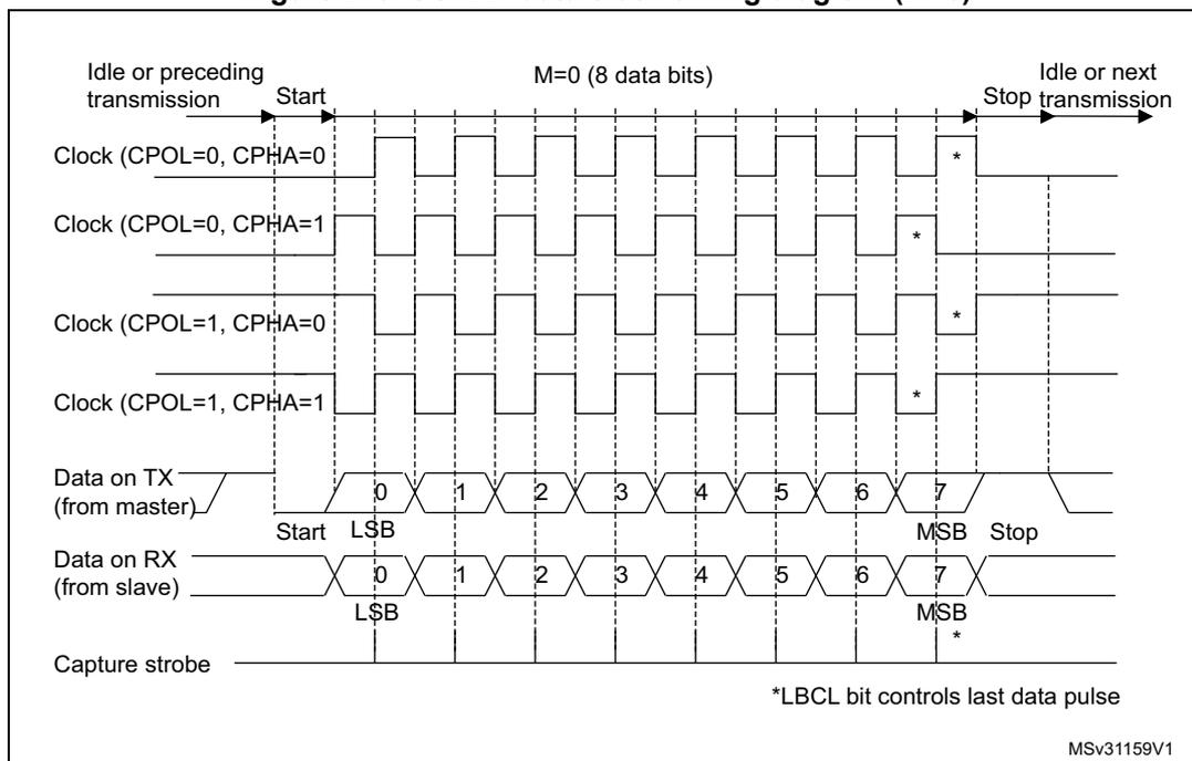
Idle or preceding transmission Start M=0 (8 data bits) Stop Idle or next transmission
Clock (CPOL=0, CPHA=0)
Clock (CPOL=0, CPHA=1)
Clock (CPOL=1, CPHA=0)
Clock (CPOL=1, CPHA=1)
Data on TX (from master) Start LSB 0 1 2 3 4 5 6 7 MSB Stop
Data on RX (from slave) LSB 0 1 2 3 4 5 6 7 MSB
Capture strobe
*LBCL bit controls last data pulse
MSv31159V1
Figure 241. USART data clock timing diagram (M=1)
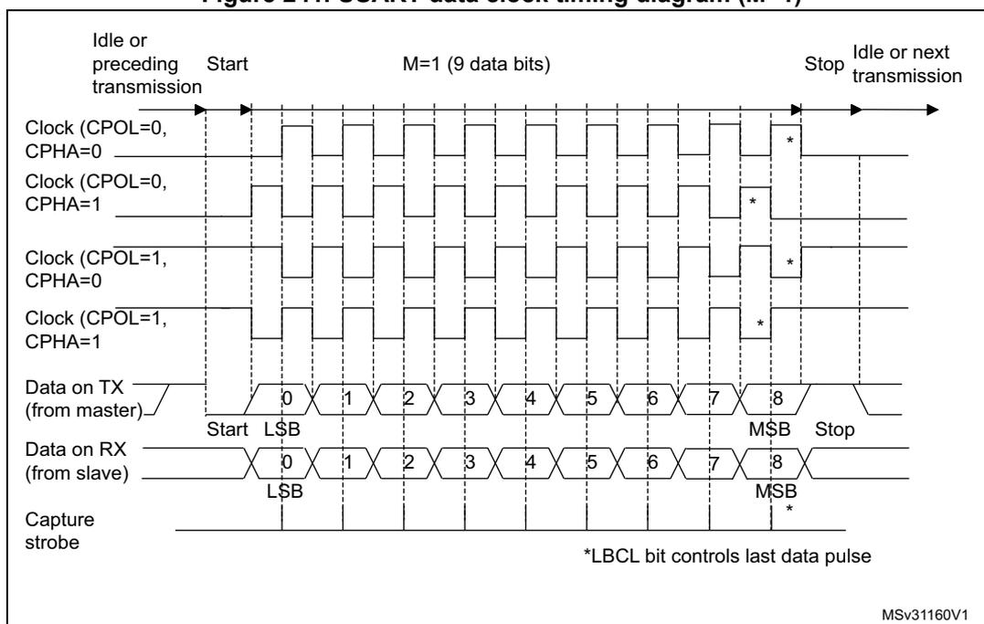
Idle or preceding transmission Start M=1 (9 data bits) Stop Idle or next transmission
Clock (CPOL=0, CPHA=0)
Clock (CPOL=0, CPHA=1)
Clock (CPOL=1, CPHA=0)
Clock (CPOL=1, CPHA=1)
Data on TX (from master) Start LSB 0 1 2 3 4 5 6 7 8 MSB Stop
Data on RX (from slave) LSB 0 1 2 3 4 5 6 7 8 MSB
Capture strobe
*LBCL bit controls last data pulse
MSv31160V1
Figure 242. RX data setup/hold time
23.4.10 USART Single-wire Half-duplex communication
Single-wire Half-duplex mode is selected by setting the HDSEL bit in the USART_CR3 register. In this mode, the following bits must be kept cleared:
- • CLKEN bit in the USART_CR2 register,
- • SCEN and IREN bits in the USART_CR3 register.
The USART can be configured to follow a Single-wire Half-duplex protocol where the TX and RX lines are internally connected. The selection between half- and Full-duplex communication is made with a control bit HDSEL in USART_CR3.
As soon as HDSEL is written to 1:
- • The TX and RX lines are internally connected
- • The RX pin is no longer used
- • The TX pin is always released when no data is transmitted. Thus, it acts as a standard I/O in idle or in reception. It means that the I/O must be configured so that TX is configured as alternate function open-drain with an external pull-up.
Apart from this, the communication protocol is similar to normal USART mode. Any conflicts on the line must be managed by software (by the use of a centralized arbiter, for instance). In particular, the transmission is never blocked by hardware and continues as soon as data is written in the data register while the TE bit is set.
For code example, refer to A.15.7: USART DMA .
23.4.11 USART continuous communication in DMA mode
The USART is capable of performing continuous communication using the DMA. The DMA requests for Rx buffer and Tx buffer are generated independently.
Note: Please refer to Section 23.3: USART implementation on page 592 to determine if the DMA mode is supported. If DMA is not supported, use the USART as explained in Section 23.4.2: USART transmitter or Section 23.4.3: USART receiver . To perform continuous communication, the user can clear the TXE/ RXNE flags In the USART_ISR register.
For code example, refer to A.15.7: USART DMA .
Transmission using DMA
DMA mode can be enabled for transmission by setting DMAT bit in the USART_CR3 register. Data is loaded from a SRAM area configured using the DMA peripheral (refer to Section 10: Direct memory access controller (DMA) on page 149 ) to the USART_TDR register whenever the TXE bit is set. To map a DMA channel for USART transmission, use the following procedure (x denotes the channel number):
- 1. Write the USART_TDR register address in the DMA control register to configure it as the destination of the transfer. The data is moved to this address from memory after each TXE event.
- 2. Write the memory address in the DMA control register to configure it as the source of the transfer. The data is loaded into the USART_TDR register from this memory area after each TXE event.
- 3. Configure the total number of bytes to be transferred to the DMA control register.
- 4. Configure the channel priority in the DMA register
- 5. Configure DMA interrupt generation after half/ full transfer as required by the application.
- 6. Clear the TC flag in the USART_ISR register by setting the TCCF bit in the USART_ICR register.
- 7. Activate the channel in the DMA register.
When the number of data transfers programmed in the DMA Controller is reached, the DMA controller generates an interrupt on the DMA channel interrupt vector.
In transmission mode, once the DMA has written all the data to be transmitted (the TCIF flag is set in the DMA_ISR register), the TC flag can be monitored to make sure that the USART communication is complete. This is required to avoid corrupting the last transmission before disabling the USART or entering Stop mode. Software must wait until TC=1. The TC flag remains cleared during all data transfers and it is set by hardware at the end of transmission of the last frame.
Figure 243. Transmission using DMA
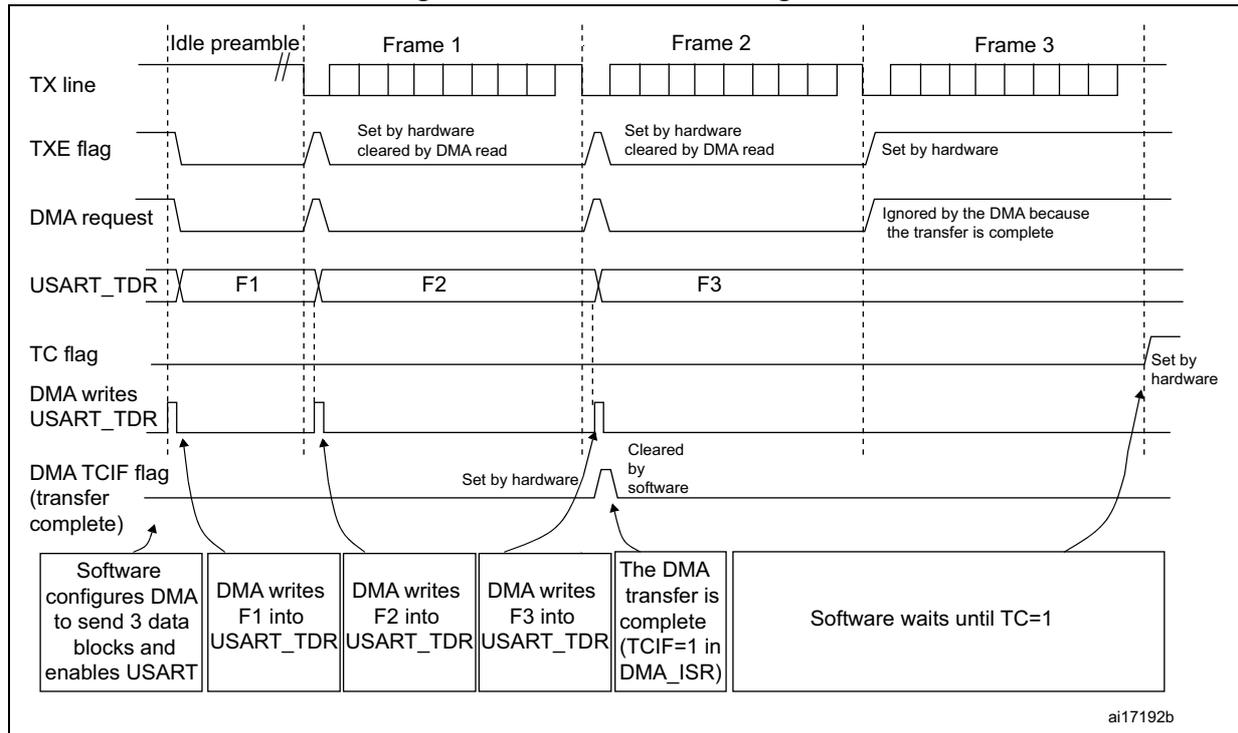
The diagram illustrates the timing for USART transmission using DMA. It shows the following signals and events:
- TX line: Shows an idle preamble followed by three frames (Frame 1, Frame 2, Frame 3). Each frame consists of 8 data blocks.
- TXE flag: Set by hardware when the USART_TDR register is empty. It is cleared by a DMA read. For Frame 1 and 2, it is set before each frame and cleared after the last data block. For Frame 3, it is set before the frame and remains set until the last data block is read.
- DMA request: Generated when the TXE flag is set. It is ignored by the DMA because the transfer is complete after Frame 2.
- USART_TDR: Shows the data blocks F1, F2, and F3 being written into the register by the DMA.
- TC flag: Set by hardware when the last data block has been transmitted. It is cleared by software.
- DMA TCIF flag (transfer complete): Set by hardware when the TC flag is set. It is cleared by software.
Sequence of events:
- Software configures DMA to send 3 data blocks and enables USART.
- DMA writes F1 into USART_TDR.
- DMA writes F2 into USART_TDR.
- DMA writes F3 into USART_TDR.
- The DMA transfer is complete (TCIF=1 in DMA_ISR).
- Software waits until TC=1.
ai17192b
Reception using DMA
DMA mode can be enabled for reception by setting the DMAR bit in USART_CR3 register. Data is loaded from the USART_RDR register to a SRAM area configured using the DMA peripheral (refer to Section 10: Direct memory access controller (DMA) on page 149 ) whenever a data byte is received. To map a DMA channel for USART reception, use the following procedure:
- 1. Write the USART_RDR register address in the DMA control register to configure it as the source of the transfer. The data is moved from this address to the memory after each RXNE event.
- 2. Write the memory address in the DMA control register to configure it as the destination of the transfer. The data is loaded from USART_RDR to this memory area after each RXNE event.
- 3. Configure the total number of bytes to be transferred to the DMA control register.
- 4. Configure the channel priority in the DMA control register
- 5. Configure interrupt generation after half/ full transfer as required by the application.
- 6. Activate the channel in the DMA control register.
When the number of data transfers programmed in the DMA Controller is reached, the DMA controller generates an interrupt on the DMA channel interrupt vector.
Figure 244. Reception using DMA
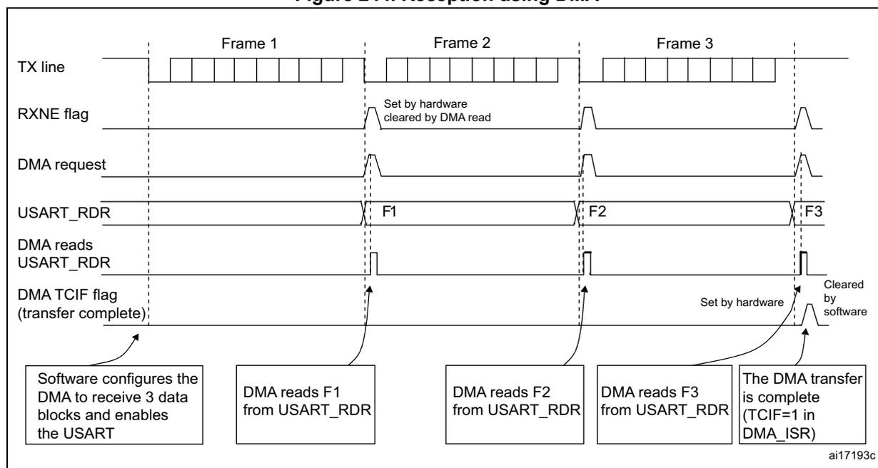
The diagram illustrates the reception of three frames (Frame 1, Frame 2, Frame 3) using DMA. The TX line shows the incoming data. The RXNE flag is set by hardware when a byte is received and cleared by a DMA read. The DMA request is generated when RXNE is set. The USART_RDR register is read by the DMA. The DMA TCIF flag is set by hardware when the transfer is complete and cleared by software. The sequence starts with software configuration, followed by DMA reads of F1, F2, and F3, and finally the transfer complete interrupt.
Timeline details:
- TX line: Shows three frames of data being received.
- RXNE flag: Set by hardware when a byte is received, cleared by DMA read.
- DMA request: Generated when RXNE is set.
- USART_RDR: Register containing the received data (F1, F2, F3).
- DMA reads USART_RDR: The DMA reads the data from the register.
- DMA TCIF flag (transfer complete): Set by hardware when the transfer is complete, cleared by software.
Annotations:
- Software configures the DMA to receive 3 data blocks and enables the USART
- DMA reads F1 from USART_RDR
- DMA reads F2 from USART_RDR
- DMA reads F3 from USART_RDR
- The DMA transfer is complete (TCIF=1 in DMA_ISR)
ai17193c
Error flagging and interrupt generation in multibuffer communication
In multibuffer communication if any error occurs during the transaction the error flag is asserted after the current byte. An interrupt is generated if the interrupt enable flag is set. For framing error, overrun error and noise flag which are asserted with RXNE in single byte reception, there is a separate error flag interrupt enable bit (EIE bit in the USART_CR3 register), which, if set, enables an interrupt after the current byte if any of these errors occur.
23.4.12 RS232 hardware flow control and RS485 driver enable using USART
It is possible to control the serial data flow between 2 devices by using the CTS input and the RTS output. The Figure 245 shows how to connect 2 devices in this mode:
Figure 245. Hardware flow control between 2 USARTs
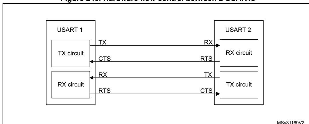
The diagram shows two USARTs, USART 1 and USART 2, connected via their TX and RX lines. USART 1's TX circuit is connected to USART 2's RX circuit. USART 1's RX circuit is connected to USART 2's TX circuit. Flow control lines are also connected: USART 1's CTS input is connected to USART 2's RTS output, and USART 1's RTS output is connected to USART 2's CTS input.
Connections:
- USART 1 TX circuit to USART 2 RX circuit
- USART 1 RX circuit to USART 2 TX circuit
- USART 1 CTS input to USART 2 RTS output
- USART 1 RTS output to USART 2 CTS input
MSv31169V2
RS232 RTS and CTS flow control can be enabled independently by writing the RTSE and CTSE bits respectively to 1 (in the USART_CR3 register).
RS232 RTS flow control
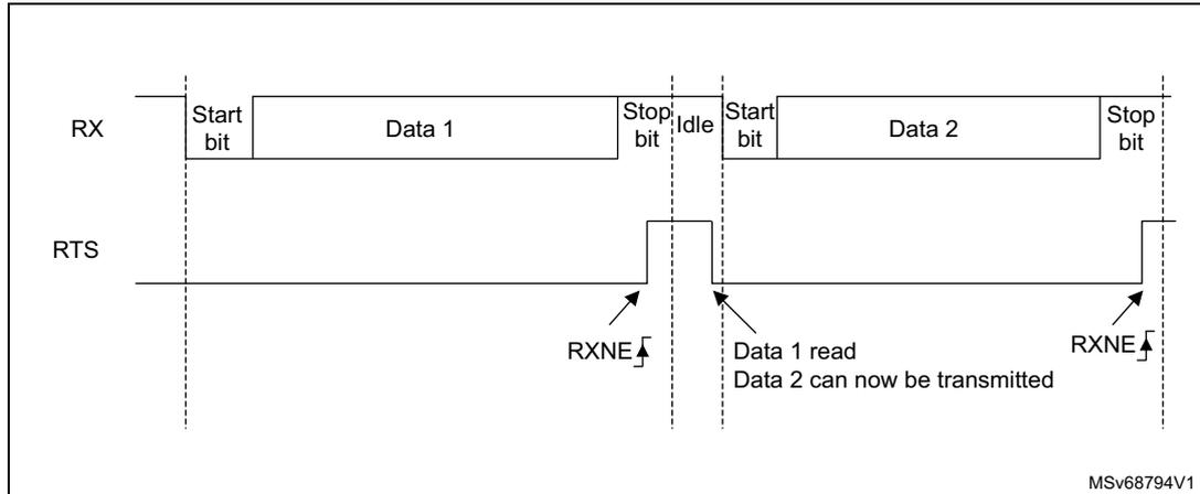
If the RTS flow control is enabled (RTSE=1), then RTS is deasserted (tied low) as long as the USART receiver is ready to receive a new data. When the receive register is full, RTS is asserted, indicating that the transmission is expected to stop at the end of the current frame. Figure 246 shows an example of communication with RTS flow control enabled.
Figure 246. RS232 RTS flow control
RS232 CTS flow control
If the CTS flow control is enabled (CTSE=1), then the transmitter checks the CTS input before transmitting the next frame. If CTS is deasserted (tied low), then the next data is transmitted (assuming that data is to be transmitted, in other words, if TXE=0), else the transmission does not occur. When CTS is asserted during a transmission, the current transmission is completed before the transmitter stops.
When CTSE=1, the CTSIF status bit is automatically set by hardware as soon as the CTS input toggles. It indicates when the receiver becomes ready or not ready for communication. An interrupt is generated if the CTSIE bit in the USART_CR3 register is set. Figure 247 shows an example of communication with CTS flow control enabled.
Figure 247. RS232 CTS flow control
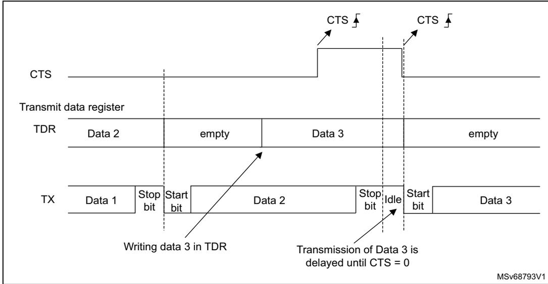
Note: For correct behavior, CTS must be deasserted at least 3 USART clock source periods before the end of the current character. In addition it should be noted that the CTSCF flag may not be set for pulses shorter than 2 x PCLK periods.
For code example, refer to A.15.8: USART hardware flow control .
RS485 Driver Enable
The driver enable feature is enabled by setting bit DEM in the USART_CR3 control register. This allows the user to activate the external transceiver control, through the DE (Driver Enable) signal. The assertion time is the time between the activation of the DE signal and the beginning of the START bit. It is programmed using the DEAT [4:0] bit fields in the USART_CR1 control register. The de-assertion time is the time between the end of the last stop bit, in a transmitted message, and the de-activation of the DE signal. It is programmed using the DEDT [4:0] bit fields in the USART_CR1 control register. The polarity of the DE signal can be configured using the DEP bit in the USART_CR3 control register.
In USART, the DEAT and DEDT are expressed in sample time units (1/8 or 1/16 bit duration, depending on the oversampling rate).
23.5 USART in low-power modes
Table 92. Effect of low-power modes on the USART
| Mode | Description |
|---|---|
| Sleep | No effect. USART interrupt causes the device to exit Sleep mode. |
| Stop | The USART is not clocked. It is not functional in Stop mode but its configuration is kept upon wake-up. |
| Standby | The USART is powered down and must be reinitialized when the device has exited from Standby mode. |
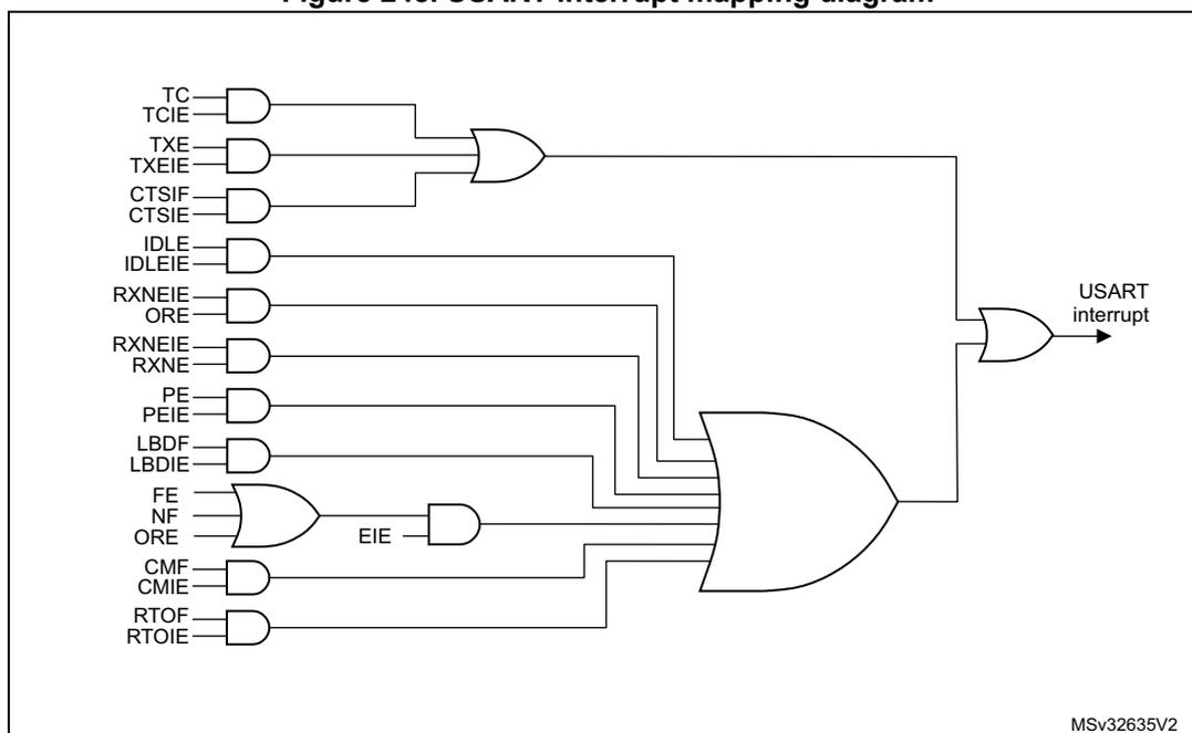
23.6 USART interrupts
Table 93. USART interrupt requests
| Interrupt event | Event flag | Enable Control bit |
|---|---|---|
| Transmit data register empty | TXE | TXEIE |
| CTS interrupt | CTSIF | CTSIE |
| Transmission Complete | TC | TCIE |
| Receive data register not empty (data ready to be read) | RXNE | RXNEIE |
| Overrun error detected | ORE | |
| Idle line detected | IDLE | IDLEIE |
| Parity error | PE | PEIE |
| Noise Flag, Overrun error and Framing Error in multibuffer communication. | NF or ORE or FE | EIE |
| Character match | CMF | CMIE |
| Receiver timeout | RTOF | RTOIE |
The USART interrupt events are connected to the same interrupt vector (see Figure 248 ).
- • During transmission: Transmission Complete, Clear to Send, Transmit data Register empty interrupt.
- • During reception: Idle Line detection, Overrun error, Receive data register not empty, Parity error, Noise Flag, Framing Error, Character match, etc.
These events generate an interrupt if the corresponding Enable Control Bit is set.
Figure 248. USART interrupt mapping diagram
23.7 USART registers
Refer to Section 1.2 on page 33 for a list of abbreviations used in register descriptions.
The peripheral registers have to be accessed by words (32 bits).
23.7.1 USART control register 1 (USART_CR1)
Address offset: 0x00
Reset value: 0x0000 0000
| 31 | 30 | 29 | 28 | 27 | 26 | 25 | 24 | 23 | 22 | 21 | 20 | 19 | 18 | 17 | 16 |
|---|---|---|---|---|---|---|---|---|---|---|---|---|---|---|---|
| Res. | Res. | Res. | M1 | Res. | RTOIE | DEAT[4:0] | DEDT[4:0] | ||||||||
| rw | rw | rw | rw | rw | rw | rw | rw | rw | rw | rw | rw | ||||
| 15 | 14 | 13 | 12 | 11 | 10 | 9 | 8 | 7 | 6 | 5 | 4 | 3 | 2 | 1 | 0 |
| OVER8 | CMIE | MME | M0 | WAKE | PCE | PS | PEIE | TXEIE | TCIE | RXNEIE | IDLEIE | TE | RE | Res. | UE |
| rw | rw | rw | rw | rw | rw | rw | rw | rw | rw | rw | rw | rw | rw | rw | |
Bits 31:29 Reserved, must be kept at reset value.
Bit 28 M1 : Word length
This bit, with bit 12 (M0), determines the word length. It is set or cleared by software.
M[1:0] = 00: 1 Start bit, 8 data bits, n stop bits
M[1:0] = 01: 1 Start bit, 9 data bits, n stop bits
M[1:0] = 10: Reserved
This bit can only be written when the USART is disabled (UE=0).
Bit 27 Reserved, must be kept at reset value.
Bit 26 RTOIE : Receiver timeout interrupt enable
This bit is set and cleared by software.
0: Interrupt is inhibited
1: An USART interrupt is generated when the RTOF bit is set in the USART_ISR register.
Note: If the USART does not support the Receiver timeout feature, this bit is reserved and must be kept at reset value. Section 23.3: USART implementation on page 592 .
Bits 25:21 DEAT[4:0] : Driver Enable assertion time
This 5-bit value defines the time between the activation of the DE (Driver Enable) signal and the beginning of the start bit. It is expressed in sample time units (1/8 or 1/16 bit duration, depending on the oversampling rate).
This bit field can only be written when the USART is disabled (UE=0).
Note: If the Driver Enable feature is not supported, this bit is reserved and must be kept at reset value. Please refer to Section 23.3: USART implementation on page 592 .
Bits 20:16 DEDT[4:0] : Driver Enable de-assertion time
This 5-bit value defines the time between the end of the last stop bit, in a transmitted message, and the de-activation of the DE (Driver Enable) signal. It is expressed in sample time units (1/8 or 1/16 bit duration, depending on the oversampling rate).
If the USART_TDR register is written during the DEDT time, the new data is transmitted only when the DEDT and DEAT times have both elapsed.
This bit field can only be written when the USART is disabled (UE=0).
Note: If the Driver Enable feature is not supported, this bit is reserved and must be kept at reset value. Please refer to Section 23.3: USART implementation on page 592 .
Bit 15 OVER8 : Oversampling mode
0: Oversampling by 16
1: Oversampling by 8
This bit can only be written when the USART is disabled (UE=0).
Note:
Bit 14 CMIE : Character match interrupt enable
This bit is set and cleared by software.
0: Interrupt is inhibited
1: A USART interrupt is generated when the CMF bit is set in the USART_ISR register.
Bit 13 MME : Mute mode enable
This bit activates the mute mode function of the USART. When set, the USART can switch between the active and mute modes, as defined by the WAKE bit. It is set and cleared by software.
0: Receiver in active mode permanently
1: Receiver can switch between mute mode and active mode.
Bit 12 M0 : Word length
This bit determines the word length. It is set or cleared by software.
0: 1 Start bit, 8 data bits, n stop bits
1: 1 Start bit, 9 data bits, n stop bits
Bit 11 WAKE : Receiver wake-up method
This bit determines the USART wake-up method from Mute mode. It is set or cleared by software.
0: Idle line
1: Address mark
This bit field can only be written when the USART is disabled (UE=0).
Bit 10 PCE : Parity control enable
This bit selects the hardware parity control (generation and detection). When the parity control is enabled, the computed parity is inserted at the MSB position (9th bit if M=1; 8th bit if M=0) and parity is checked on the received data. This bit is set and cleared by software. Once it is set, PCE is active after the current byte (in reception and in transmission).
0: Parity control disabled
1: Parity control enabled
This bit field can only be written when the USART is disabled (UE=0).
Bit 9 PS : Parity selection
This bit selects the odd or even parity when the parity generation/detection is enabled (PCE bit set). It is set and cleared by software. The parity is selected after the current byte.
0: Even parity
1: Odd parity
This bit field can only be written when the USART is disabled (UE=0).
Bit 8 PEIE : PE interrupt enable
This bit is set and cleared by software.
0: Interrupt is inhibited
1: A USART interrupt is generated whenever PE=1 in the USART_ISR register
Bit 7 TXEIE : interrupt enable
This bit is set and cleared by software.
0: Interrupt is inhibited
1: A USART interrupt is generated whenever TXE=1 in the USART_ISR register
Bit 6 TCIE: Transmission complete interrupt enableThis bit is set and cleared by software.
0: Interrupt is inhibited
1: A USART interrupt is generated whenever TC=1 in the USART_ISR register
Bit 5 RXNEIE: RXNE interrupt enableThis bit is set and cleared by software.
0: Interrupt is inhibited
1: A USART interrupt is generated whenever ORE=1 or RXNE=1 in the USART_ISR register
Bit 4 IDLEIE: IDLE interrupt enableThis bit is set and cleared by software.
0: Interrupt is inhibited
1: A USART interrupt is generated whenever IDLE=1 in the USART_ISR register
Bit 3 TE: Transmitter enableThis bit enables the transmitter. It is set and cleared by software.
0: Transmitter is disabled
1: Transmitter is enabled
During transmission, a “0” pulse on the TE bit (“0” followed by “1”) sends a preamble (idle line) after the current word. In order to generate an idle character, the TE must not be immediately written to 1.
Bit 2 RE: Receiver enableThis bit enables the receiver. It is set and cleared by software.
0: Receiver is disabled
1: Receiver is enabled and begins searching for a start bit
Bit 1 Reserved, must be kept at reset value. Bit 0 UE: USART enableWhen this bit is cleared, the USART prescalers and outputs are stopped immediately, and current operations are discarded. The configuration of the USART is kept, but all the status flags, in the USART_ISR are set to their default values. This bit is set and cleared by software.
0: USART prescaler and outputs disabled, low-power mode
1: USART enabled
Note: In order to go into low-power mode without generating errors on the line, the TE bit must be reset before and the software must wait for the TC bit in the USART_ISR to be set before resetting the UE bit.
The DMA requests are also reset when UE = 0 so the DMA channel must be disabled before resetting the UE bit.
23.7.2 USART control register 2 (USART_CR2)
Address offset: 0x04
Reset value: 0x0000 0000
| 31 | 30 | 29 | 28 | 27 | 26 | 25 | 24 | 23 | 22 | 21 | 20 | 19 | 18 | 17 | 16 |
|---|---|---|---|---|---|---|---|---|---|---|---|---|---|---|---|
| ADD[7:4] | ADD[3:0] | RTOEN | ABRMOD[1:0] | ABREN | MSBFIRST | DATAINV | TXINV | RXINV | |||||||
| rw | rw | rw | rw | rw | rw | rw | rw | rw | rw | rw | rw | rw | rw | rw | rw |
| 15 | 14 | 13 | 12 | 11 | 10 | 9 | 8 | 7 | 6 | 5 | 4 | 3 | 2 | 1 | 0 |
| SWAP | Res. | STOP[1:0] | CLKEN | CPOL | CPHA | LBCL | Res. | Res. | Res. | ADDM7 | Res. | Res. | Res. | Res. | |
| rw | rw | rw | rw | rw | rw | rw | rw | ||||||||
Bits 31:28 ADD[7:4]: Address of the USART node
This bit-field gives the address of the USART node or a character code to be recognized.
This is used in multiprocessor communication during Mute mode or Stop mode, for wake-up with 7-bit address mark detection. The MSB of the character sent by the transmitter should be equal to 1. It may also be used for character detection during normal reception, Mute mode inactive. In this case, the whole received character (8-bit) is compared to the ADD[7:0] value and CMF flag is set on match.
This bit field can only be written when reception is disabled (RE = 0) or the USART is disabled (UE=0)
Bits 27:24 ADD[3:0]: Address of the USART node
This bit-field gives the address of the USART node or a character code to be recognized.
This is used in multiprocessor communication during Mute mode or Stop mode, for wake-up with address mark detection.
This bit field can only be written when reception is disabled (RE = 0) or the USART is disabled (UE=0)
Bit 23 RTOEN: Receiver timeout enable
This bit is set and cleared by software.
0: Receiver timeout feature disabled.
1: Receiver timeout feature enabled.
When this feature is enabled, the RTOF flag in the USART_ISR register is set if the RX line is idle (no reception) for the duration programmed in the RTOR (receiver timeout register).
Note: If the USART does not support the Receiver timeout feature, this bit is reserved and must be kept at reset value. Please refer to Section 23.3: USART implementation on page 592.
Bits 22:21 ABRMOD[1:0]: Auto baud rate mode
These bits are set and cleared by software.
00: Measurement of the start bit is used to detect the baud rate.
01: Falling edge to falling edge measurement. (the received frame must start with a single bit = 1 -> Frame = Start10xxxxxx)
10: 0x7F frame detection.
11: 0x55 frame detection
This bit field can only be written when ABREN = 0 or the USART is disabled (UE=0).
Note: If DATAINV=1 and/or MSBFIRST=1 the patterns must be the same on the line, for example 0xAA for MSBFIRST)
If the USART does not support the auto baud rate feature, this bit is reserved and must be kept at reset value. Please refer to Section 23.3: USART implementation on page 592.
Bit 20 ABREN: Auto baud rate enableThis bit is set and cleared by software.
0: Auto baud rate detection is disabled.
1: Auto baud rate detection is enabled.
Note: If the USART does not support the auto baud rate feature, this bit is reserved and must be kept at reset value. Please refer to Section 23.3: USART implementation on page 592 .
Bit 19 MSBFIRST: Most significant bit firstThis bit is set and cleared by software.
0: data is transmitted/received with data bit 0 first, following the start bit.
1: data is transmitted/received with the MSB (bit 7/8/9) first, following the start bit.
This bit field can only be written when the USART is disabled (UE=0).
Bit 18 DATAINV: Binary data inversionThis bit is set and cleared by software.
0: Logical data from the data register are send/received in positive/direct logic. (1=H, 0=L)
1: Logical data from the data register are send/received in negative/inverse logic. (1=L, 0=H). The parity bit is also inverted.
This bit field can only be written when the USART is disabled (UE=0).
Bit 17 TXINV: TX pin active level inversionThis bit is set and cleared by software.
0: TX pin signal works using the standard logic levels ( \( V_{DD} \) =1/idle, Gnd=0/mark)
1: TX pin signal values are inverted. ( \( V_{DD} \) =0/mark, Gnd=1/idle).
This allows the use of an external inverter on the TX line.
This bit field can only be written when the USART is disabled (UE=0).
Bit 16 RXINV: RX pin active level inversionThis bit is set and cleared by software.
0: RX pin signal works using the standard logic levels ( \( V_{DD} \) =1/idle, Gnd=0/mark)
1: RX pin signal values are inverted. ( \( V_{DD} \) =0/mark, Gnd=1/idle).
This allows the use of an external inverter on the RX line.
This bit field can only be written when the USART is disabled (UE=0).
Bit 15 SWAP: Swap TX/RX pinsThis bit is set and cleared by software.
0: TX/RX pins are used as defined in standard pinout
1: The TX and RX pins functions are swapped. This allows to work in the case of a cross-wired connection to another USART.
This bit field can only be written when the USART is disabled (UE=0).
Bit 14 Reserved, must be kept at reset value. Bits 13:12 STOP[1:0]: STOP bitsThese bits are used for programming the stop bits.
00: 1 stop bit
01: Reserved
10: 2 stop bits
11: Reserved
This bit field can only be written when the USART is disabled (UE=0).
Bit 11 CLKEN: Clock enableThis bit allows the user to enable the CK pin.
0: CK pin disabled
1: CK pin enabled
This bit can only be written when the USART is disabled (UE=0).
Note: If synchronous mode is not supported, this bit is reserved and must be kept at reset value. Please refer to Section 23.3: USART implementation on page 592.
Bit 10 CPOL: Clock polarityThis bit allows the user to select the polarity of the clock output on the CK pin in synchronous mode. It works in conjunction with the CPHA bit to produce the desired clock/data relationship
0: Steady low value on CK pin outside transmission window
1: Steady high value on CK pin outside transmission window
This bit can only be written when the USART is disabled (UE=0).
Note: If synchronous mode is not supported, this bit is reserved and must be kept at reset value. Please refer to Section 23.3: USART implementation on page 592.
Bit 9 CPHA: Clock phaseThis bit is used to select the phase of the clock output on the CK pin in synchronous mode. It works in conjunction with the CPOL bit to produce the desired clock/data relationship (see Figure 240 and Figure 241)
0: The first clock transition is the first data capture edge
1: The second clock transition is the first data capture edge
This bit can only be written when the USART is disabled (UE=0).
Note: If synchronous mode is not supported, this bit is reserved and must be kept at reset value. Please refer to Section 23.3: USART implementation on page 592.
Bit 8 LBCL: Last bit clock pulseThis bit is used to select whether the clock pulse associated with the last data bit transmitted (MSB) has to be output on the CK pin in synchronous mode.
0: The clock pulse of the last data bit is not output to the CK pin
1: The clock pulse of the last data bit is output to the CK pin
Caution: The last bit is the 7th or 8th or 9th data bit transmitted depending on the 7 or 8 or 9 bit format selected by the M bit in the USART_CR1 register.
This bit can only be written when the USART is disabled (UE=0).
Note: If synchronous mode is not supported, this bit is reserved and must be kept at reset value. Please refer to Section 23.3: USART implementation on page 592.
Bits 7:5 Reserved, must be kept at reset value.
Bit 4 ADDM7: 7-bit Address Detection/4-bit Address DetectionThis bit is for selection between 4-bit address detection or 7-bit address detection.
0: 4-bit address detection
1: 7-bit address detection (in 8-bit data mode)
This bit can only be written when the USART is disabled (UE=0)
Note: In 7-bit and 9-bit data modes, the address detection is done on 6-bit and 8-bit address (ADD[5:0] and ADD[7:0]) respectively.
Bits 3:0 Reserved, must be kept at reset value.
Note: The 3 bits (CPOL, CPHA, LBCL) should not be written while the transmitter is enabled.
23.7.3 USART control register 3 (USART_CR3)
Address offset: 0x08
Reset value: 0x0000 0000
| 31 | 30 | 29 | 28 | 27 | 26 | 25 | 24 | 23 | 22 | 21 | 20 | 19 | 18 | 17 | 16 |
|---|---|---|---|---|---|---|---|---|---|---|---|---|---|---|---|
| Res. | Res. | Res. | Res. | Res. | Res. | Res. | Res. | Res. | Res. | Res. | Res. | Res. | Res. | Res. | Res. |
| 15 | 14 | 13 | 12 | 11 | 10 | 9 | 8 | 7 | 6 | 5 | 4 | 3 | 2 | 1 | 0 |
| DEP | DEM | DDRE | OVRDIS | ONEBIT | CTSIE | CTSE | RTSE | DMAT | DMAR | Res. | Res. | HDSEL | Res. | Res. | EIE |
| rw | rw | rw | rw | rw | rw | rw | rw | rw | rw | rw | rw |
Bits 31:25 Reserved, must be kept at reset value.
Bit 24 Reserved, must be kept at reset value.
Bit 23 Reserved, must be kept at reset value.
Bits 19:17 Reserved, must be kept at reset value.
Bit 16 Reserved, must be kept at reset value.
Bit 15 DEP : Driver enable polarity selection
0: DE signal is active high.
1: DE signal is active low.
This bit can only be written when the USART is disabled (UE=0).
Note: If the Driver Enable feature is not supported, this bit is reserved and must be kept at reset value. Please refer to Section 23.3: USART implementation on page 592 .
Bit 14 DEM : Driver enable mode
This bit allows the user to activate the external transceiver control, through the DE signal.
0: DE function is disabled.
1: DE function is enabled. The DE signal is output on the RTS pin.
This bit can only be written when the USART is disabled (UE=0).
Note: If the Driver Enable feature is not supported, this bit is reserved and must be kept at reset value. Section 23.3: USART implementation on page 592 .
Bit 13 DDRE : DMA Disable on Reception Error
0: DMA is not disabled in case of reception error. The corresponding error flag is set but RXNE is kept 0 preventing from overrun. As a consequence, the DMA request is not asserted, so the erroneous data is not transferred (no DMA request), but next correct received data are transferred.
1: DMA is disabled following a reception error. The corresponding error flag is set, as well as RXNE. The DMA request is masked until the error flag is cleared. This means that the software must first disable the DMA request (DMAR = 0) or clear RXNE before clearing the error flag.
This bit can only be written when the USART is disabled (UE=0).
Note: The reception errors are: parity error, framing error or noise error.
Bit 12 OVRDIS : Overrun DisableThis bit is used to disable the receive overrun detection.
0: Overrun Error Flag, ORE, is set when received data is not read before receiving new data.
1: Overrun functionality is disabled. If new data is received while the RXNE flag is still set the ORE flag is not set and the new received data overwrites the previous content of the USART_RDR register.
This bit can only be written when the USART is disabled (UE=0).
Note: This control bit allows checking the communication flow without reading the data.
Bit 11 ONEBIT : One sample bit method enableThis bit allows the user to select the sample method. When the one sample bit method is selected the noise detection flag (NF) is disabled.
0: Three sample bit method
1: One sample bit method
This bit can only be written when the USART is disabled (UE=0).
Note: ONEBIT feature applies only to data bits, It does not apply to Start bit.
Bit 10 CTSIE : CTS interrupt enable0: Interrupt is inhibited
1: An interrupt is generated whenever CTSIF=1 in the USART_ISR register
Note: If the hardware flow control feature is not supported, this bit is reserved and must be kept at reset value. Please refer to Section 23.3: USART implementation on page 592.
Bit 9 CTSE : CTS enable0: CTS hardware flow control disabled
1: CTS mode enabled, data is only transmitted when the CTS input is deasserted (tied to 0). If the CTS input is asserted while data is being transmitted, then the transmission is completed before stopping. If data is written into the data register while CTS is asserted, the transmission is postponed until CTS is deasserted.
This bit can only be written when the USART is disabled (UE=0)
Note: If the hardware flow control feature is not supported, this bit is reserved and must be kept at reset value. Please refer to Section 23.3: USART implementation on page 592.
Bit 8 RTSE : RTS enable0: RTS hardware flow control disabled
1: RTS output enabled, data is only requested when there is space in the receive buffer. The transmission of data is expected to cease after the current character has been transmitted. The RTS output is deasserted (pulled to 0) when data can be received.
This bit can only be written when the USART is disabled (UE=0).
Note: If the hardware flow control feature is not supported, this bit is reserved and must be kept at reset value. Please refer to Section 23.3: USART implementation on page 592.
Bit 7 DMAT : DMA enable transmitterThis bit is set/reset by software
1: DMA mode is enabled for transmission
0: DMA mode is disabled for transmission
Bit 6 DMAR : DMA enable receiverThis bit is set/reset by software
1: DMA mode is enabled for reception
0: DMA mode is disabled for reception
Bits 5:4 Reserved, must be kept at reset value.
Bit 3 HDSEL : Half-duplex selection
Selection of Single-wire Half-duplex mode
0: Half duplex mode is not selected
1: Half duplex mode is selected
This bit can only be written when the USART is disabled (UE=0).
Bits 2:1 Reserved, must be kept at reset value.
Bit 0 EIE : Error interrupt enable
Error Interrupt Enable Bit is required to enable interrupt generation in case of a framing error, overrun error or noise flag (FE=1 or ORE=1 or NF=1 in the USART_ISR register).
0: Interrupt is inhibited
1: An interrupt is generated when FE=1 or ORE=1 or NF=1 in the USART_ISR register.
23.7.4 USART baud rate register (USART_BRR)
This register can only be written when the USART is disabled (UE=0). It may be automatically updated by hardware in auto baud rate detection mode.
Address offset: 0x0C
Reset value: 0x0000 0000
| 31 | 30 | 29 | 28 | 27 | 26 | 25 | 24 | 23 | 22 | 21 | 20 | 19 | 18 | 17 | 16 |
|---|---|---|---|---|---|---|---|---|---|---|---|---|---|---|---|
| Res. | Res. | Res. | Res. | Res. | Res. | Res. | Res. | Res. | Res. | Res. | Res. | Res. | Res. | Res. | Res. |
| 15 | 14 | 13 | 12 | 11 | 10 | 9 | 8 | 7 | 6 | 5 | 4 | 3 | 2 | 1 | 0 |
| BRR[15:0] | |||||||||||||||
| rw | rw | rw | rw | rw | rw | rw | rw | rw | rw | rw | rw | rw | rw | rw | rw |
Bits 31:16 Reserved, must be kept at reset value.
Bits 15:4 BRR[15:4]
BRR[15:4] = USARTDIV[15:4]
Bits 3:0 BRR[3:0]
When OVER8 = 0, BRR[3:0] = USARTDIV[3:0].
When OVER8 = 1:
BRR[2:0] = USARTDIV[3:0] shifted 1 bit to the right.
BRR[3] must be kept cleared.
23.7.5 USART receiver timeout register (USART_RTOR)
Address offset: 0x14
Reset value: 0x0000 0000
| 31 | 30 | 29 | 28 | 27 | 26 | 25 | 24 | 23 | 22 | 21 | 20 | 19 | 18 | 17 | 16 |
|---|---|---|---|---|---|---|---|---|---|---|---|---|---|---|---|
| Res. | Res. | Res. | Res. | Res. | Res. | Res. | Res. | RTO[23:16] | |||||||
| rw | rw | rw | rw | rw | rw | rw | rw | ||||||||
| 15 | 14 | 13 | 12 | 11 | 10 | 9 | 8 | 7 | 6 | 5 | 4 | 3 | 2 | 1 | 0 |
| RTO[15:0] | |||||||||||||||
| rw | rw | rw | rw | rw | rw | rw | rw | rw | rw | rw | rw | rw | rw | rw | rw |
Bits 31:24 Reserved, must be kept at reset value.
Bits 23:0 RTO[23:0] : Receiver timeout value
This bit-field gives the Receiver timeout value in terms of number of bit duration.
In standard mode, the RTOF flag is set if, after the last received character, no new start bit is detected for more than the RTO value.
Note: This value must only be programmed once per received character.
Note: RTOR can be written on the fly. If the new value is lower than or equal to the counter, the RTOF flag is set.
This register is reserved and forced by hardware to “0x00000000” when the Receiver timeout feature is not supported. Please refer to Section 23.3: USART implementation on page 592 .
23.7.6 USART request register (USART_RQR)
Address offset: 0x18
Reset value: 0x0000 0000
| 31 | 30 | 29 | 28 | 27 | 26 | 25 | 24 | 23 | 22 | 21 | 20 | 19 | 18 | 17 | 16 |
|---|---|---|---|---|---|---|---|---|---|---|---|---|---|---|---|
| Res. | Res. | Res. | Res. | Res. | Res. | Res. | Res. | Res. | Res. | Res. | Res. | Res. | Res. | Res. | Res. |
| 15 | 14 | 13 | 12 | 11 | 10 | 9 | 8 | 7 | 6 | 5 | 4 | 3 | 2 | 1 | 0 |
| Res. | Res. | Res. | Res. | Res. | Res. | Res. | Res. | Res. | Res. | Res. | Res. | RXFRQ | MMRQ | SBKRQ | ABRRQ |
| w | w | w | w |
Bits 31:4 Reserved, must be kept at reset value.
Bit 3 RXFRQ : Receive data flush request
Writing 1 to this bit clears the RXNE flag.
This allows to discard the received data without reading it, and avoid an overrun condition.
Bit 2 MMRQ : Mute mode request
Writing 1 to this bit puts the USART in mute mode and sets the RWU flag.
Bit 1 SBKRQ : Send break request
Writing 1 to this bit sets the SBKF flag and request to send a BREAK on the line, as soon as the transmit machine is available.
Note: In the case the application needs to send the break character following all previously inserted data, including the ones not yet transmitted, the software should wait for the TXE flag assertion before setting the SBKRQ bit.
Bit 0 ABRRQ : Auto baud rate request
Writing 1 to this bit resets the ABRF and ABRE flags in the USART_ISR and request an automatic baud rate measurement on the next received data frame.
Note: If the USART does not support the auto baud rate feature, this bit is reserved and must be kept at reset value. Please refer to Section 23.3: USART implementation on page 592 .
23.7.7 USART interrupt and status register (USART_ISR)
Address offset: 0x1C
Reset value: 0x0200 00C0
| 31 | 30 | 29 | 28 | 27 | 26 | 25 | 24 | 23 | 22 | 21 | 20 | 19 | 18 | 17 | 16 |
|---|---|---|---|---|---|---|---|---|---|---|---|---|---|---|---|
| Res. | Res. | Res. | Res. | Res. | Res. | Res. | Res. | Res. | Res. | Res. | Res. | RWU | SBKF | CMF | BUSY |
| r | r | r | r | ||||||||||||
| 15 | 14 | 13 | 12 | 11 | 10 | 9 | 8 | 7 | 6 | 5 | 4 | 3 | 2 | 1 | 0 |
| ABRF | ABRE | Res. | Res. | RTOF | CTS | CTSIF | Res. | TXE | TC | RXNE | IDLE | ORE | NF | FE | PE |
| r | r | r | r | r | r | r | r | r | r | r | r | r |
Bits 31:25 Reserved, must be kept at reset value.
Bits 24:22 Reserved, must be kept at reset value.
Bit 21 Reserved, must be kept at reset value
Bit 20 Reserved, must be kept at reset value.
Bit 19 RWU : Receiver wake-up from Mute mode
This bit indicates if the USART is in mute mode. It is cleared/set by hardware when a wake-up/mute sequence is recognized. The mute mode control sequence (address or IDLE) is selected by the WAKE bit in the USART_CR1 register.
When wake-up on IDLE mode is selected, this bit can only be set by software, writing 1 to the MMRQ bit in the USART_RQR register.
0: Receiver in active mode
1: Receiver in mute mode
Bit 18 SBKF : Send break flag
This bit indicates that a send break character was requested. It is set by software, by writing 1 to the SBKRQ bit in the USART_RQR register. It is automatically reset by hardware during the stop bit of break transmission.
0: No break character is transmitted
1: Break character is transmitted
Bit 17 CMF : Character match flag
This bit is set by hardware, when the character defined by ADD[7:0] is received. It is cleared by software, writing 1 to the CMCF in the USART_ICR register.
An interrupt is generated if CMIE=1 in the USART_CR1 register.
0: No Character match detected
1: Character Match detected
Bit 16 BUSY : Busy flag
This bit is set and reset by hardware. It is active when a communication is ongoing on the RX line (successful start bit detected). It is reset at the end of the reception (successful or not).
0: USART is idle (no reception)
1: Reception on going
Bit 15 ABRF : Auto baud rate flagThis bit is set by hardware when the automatic baud rate has been set (RXNE will also be set, generating an interrupt if RXNEIE = 1) or when the auto baud rate operation was completed without success (ABRE=1) (ABRE, RXNE and FE are also set in this case)
It is cleared by software, in order to request a new auto baud rate detection, by writing 1 to the ABRRQ in the USART_RQR register.
Note: If the USART does not support the auto baud rate feature, this bit is reserved and kept at reset value.
Bit 14 ABRE : Auto baud rate errorThis bit is set by hardware if the baud rate measurement failed (baud rate out of range or character comparison failed)
It is cleared by software, by writing 1 to the ABRRQ bit in the USART_RQR register.
Note: If the USART does not support the auto baud rate feature, this bit is reserved and kept at reset value.
Bits 13:12 Reserved, must be kept at reset value.
Bit 11 RTOF : Receiver timeoutThis bit is set by hardware when the timeout value, programmed in the RTOR register has lapsed, without any communication. It is cleared by software, writing 1 to the RTOCF bit in the USART_ICR register.
An interrupt is generated if RTOIE=1 in the USART_CR1 register.
0: Timeout value not reached
1: Timeout value reached without any data reception
Note: If a time equal to the value programmed in RTOR register separates 2 characters, RTOF is not set. If this time exceeds this value + 2 sample times (2/16 or 2/8, depending on the oversampling method), RTOF flag is set.
The counter counts even if RE = 0 but RTOF is set only when RE = 1. If the timeout has already elapsed when RE is set, then RTOF is set.
If the USART does not support the Receiver timeout feature, this bit is reserved and kept at reset value.
Bit 10 CTS : CTS flagThis bit is set/reset by hardware. It is an inverted copy of the status of the CTS input pin.
0: CTS line set
1: CTS line reset
Note: If the hardware flow control feature is not supported, this bit is reserved and kept at reset value.
Bit 9 CTSIF : CTS interrupt flagThis bit is set by hardware when the CTS input toggles, if the CTSE bit is set. It is cleared by software, by writing 1 to the CTSCF bit in the USART_ICR register.
An interrupt is generated if CTSIE=1 in the USART_CR3 register.
0: No change occurred on the CTS status line
1: A change occurred on the CTS status line
Note: If the hardware flow control feature is not supported, this bit is reserved and kept at reset value.
Bit 8 Reserved, must be kept at reset value.
Bit 7 TXE: Transmit data register emptyThis bit is set by hardware when the content of the USART_TDR register has been transferred into the shift register. It is cleared by a write to the USART_TDR register.
An interrupt is generated if the TXEIE bit =1 in the USART_CR1 register.
0: data is not transferred to the shift register
1: data is transferred to the shift register)
Note: This bit is used during single buffer transmission.
Bit 6 TC: Transmission completeThis bit is set by hardware if the transmission of a frame containing data is complete and if TXE is set. An interrupt is generated if TCIE=1 in the USART_CR1 register. It is cleared by software, writing 1 to the TCCF in the USART_ICR register or by a write to the USART_TDR register.
An interrupt is generated if TCIE=1 in the USART_CR1 register.
0: Transmission is not complete
1: Transmission is complete
Note: If TE bit is reset and no transmission is on going, the TC bit is set immediately.
Bit 5 RXNE: Read data register not emptyThis bit is set by hardware when the content of the RDR shift register has been transferred to the USART_RDR register. It is cleared by a read to the USART_RDR register. The RXNE flag can also be cleared by writing 1 to the RXFRQ in the USART_RQR register.
An interrupt is generated if RXNEIE=1 in the USART_CR1 register.
0: data is not received
1: Received data is ready to be read.
Bit 4 IDLE: Idle line detectedThis bit is set by hardware when an Idle Line is detected. An interrupt is generated if IDLEIE=1 in the USART_CR1 register. It is cleared by software, writing 1 to the IDLECF in the USART_ICR register.
0: No Idle line is detected
1: Idle line is detected
Note: The IDLE bit will not be set again until the RXNE bit has been set (i.e. a new idle line occurs).
If mute mode is enabled (MME=1), IDLE is set if the USART is not mute (RWU=0), whatever the mute mode selected by the WAKE bit. If RWU=1, IDLE is not set.
Bit 3 ORE: Overrun errorThis bit is set by hardware when the data currently being received in the shift register is ready to be transferred into the RDR register while RXNE=1. It is cleared by a software, writing 1 to the ORECF, in the USART_ICR register.
An interrupt is generated if RXNEIE=1 in the USART_CR1 register, or EIE = 1 in the USART_CR3 register.
0: No overrun error
1: Overrun error is detected
Note: When this bit is set, the RDR register content is not lost but the shift register is overwritten. An interrupt is generated if the ORE flag is set during multibuffer communication if the EIE bit is set.
This bit is permanently forced to 0 (no overrun detection) when the OVRDIS bit is set in the USART_CR3 register.
Bit 2 NF : START bit Noise detection flag
This bit is set by hardware when noise is detected on a received frame. It is cleared by software, writing 1 to the NFCF bit in the USART_ICR register.
0: No noise is detected
1: Noise is detected
Note: This bit does not generate an interrupt as it appears at the same time as the RXNE bit which itself generates an interrupt. An interrupt is generated when the NF flag is set during multibuffer communication if the EIE bit is set.
Note: When the line is noise-free, the NF flag can be disabled by programming the ONEBIT bit to 1 to increase the USART tolerance to deviations (Refer to Section 23.4.5: Tolerance of the USART receiver to clock deviation on page 606 ).
Bit 1 FE : Framing error
This bit is set by hardware when a de-synchronization, excessive noise or a break character is detected. It is cleared by software, writing 1 to the FECF bit in the USART_ICR register.
An interrupt is generated if EIE = 1 in the USART_CR3 register.
0: No Framing error is detected
1: Framing error or break character is detected
Bit 0 PE : Parity error
This bit is set by hardware when a parity error occurs in receiver mode. It is cleared by software, writing 1 to the PECF in the USART_ICR register.
An interrupt is generated if PEIE = 1 in the USART_CR1 register.
0: No parity error
1: Parity error
23.7.8 USART interrupt flag clear register (USART_ICR)
Address offset: 0x20
Reset value: 0x0000 0000
| 31 | 30 | 29 | 28 | 27 | 26 | 25 | 24 | 23 | 22 | 21 | 20 | 19 | 18 | 17 | 16 |
|---|---|---|---|---|---|---|---|---|---|---|---|---|---|---|---|
| Res. | Res. | Res. | Res. | Res. | Res. | Res. | Res. | Res. | Res. | Res. | Res. | Res. | Res. | CMCF | Res. |
| rc_w1 | |||||||||||||||
| 15 | 14 | 13 | 12 | 11 | 10 | 9 | 8 | 7 | 6 | 5 | 4 | 3 | 2 | 1 | 0 |
| Res. | Res. | Res. | Res. | RTOCF | Res. | CTSCF | Res. | Res. | TCCF | Res. | IDLECF | ORECF | NCF | FECF | PECF |
| rc_w1 | rc_w1 | rc_w1 | rc_w1 | rc_w1 | rc_w1 | rc_w1 | rc_w1 |
Bits 31:20 Reserved, must be kept at reset value.
Bits 19:18 Reserved, must be kept at reset value.
Bit 17 CMCF : Character match clear flag
Writing 1 to this bit clears the CMF flag in the USART_ISR register.
Bits 16:12 Reserved, must be kept at reset value.
Bit 11 RTOCF : Receiver timeout clear flag
Writing 1 to this bit clears the RTOF flag in the USART_ISR register.
Note: If the USART does not support the Receiver timeout feature, this bit is reserved and must be kept at reset value. Please refer to Section 23.3: USART implementation on page 592 .
Bit 10 Reserved, must be kept at reset value.
Bit 9 CTSCF : CTS clear flag
Writing 1 to this bit clears the CTSIF flag in the USART_ISR register.
Note: If the hardware flow control feature is not supported, this bit is reserved and must be kept at reset value. Please refer to Section 23.3: USART implementation on page 592 .
Bit 8 Reserved, must be kept at reset value.
Bit 7 Reserved, must be kept at reset value.
Bit 6 TCCF : Transmission complete clear flag
Writing 1 to this bit clears the TC flag in the USART_ISR register.
Bit 5 Reserved, must be kept at reset value.
Bit 4 IDLECF : Idle line detected clear flag
Writing 1 to this bit clears the IDLE flag in the USART_ISR register.
Bit 3 ORECF : Overrun error clear flag
Writing 1 to this bit clears the ORE flag in the USART_ISR register.
Bit 2 NCF : Noise detected clear flag
Writing 1 to this bit clears the NF flag in the USART_ISR register.
Bit 1 FECEF : Framing error clear flag
Writing 1 to this bit clears the FE flag in the USART_ISR register.
Bit 0 PECF : Parity error clear flag
Writing 1 to this bit clears the PE flag in the USART_ISR register.
23.7.9 USART receive data register (USART_RDR)
Address offset: 0x24
Reset value: 0x0000 0000
| 31 | 30 | 29 | 28 | 27 | 26 | 25 | 24 | 23 | 22 | 21 | 20 | 19 | 18 | 17 | 16 |
|---|---|---|---|---|---|---|---|---|---|---|---|---|---|---|---|
| Res. | Res. | Res. | Res. | Res. | Res. | Res. | Res. | Res. | Res. | Res. | Res. | Res. | Res. | Res. | Res. |
| 15 | 14 | 13 | 12 | 11 | 10 | 9 | 8 | 7 | 6 | 5 | 4 | 3 | 2 | 1 | 0 |
| Res. | Res. | Res. | Res. | Res. | Res. | Res. | RDR[8:0] | ||||||||
| r | r | r | r | r | r | r | r | r | |||||||
Bits 31:9 Reserved, must be kept at reset value.
Bits 8:0 RDR[8:0] : Receive data value
Contains the received data character.
The RDR register provides the parallel interface between the input shift register and the internal bus (see Figure 230 ).
When receiving with the parity enabled, the value read in the MSB bit is the received parity bit.
23.7.10 USART transmit data register (USART_TDR)
Address offset: 0x28
Reset value: 0x0000 0000
| 31 | 30 | 29 | 28 | 27 | 26 | 25 | 24 | 23 | 22 | 21 | 20 | 19 | 18 | 17 | 16 |
|---|---|---|---|---|---|---|---|---|---|---|---|---|---|---|---|
| Res. | Res. | Res. | Res. | Res. | Res. | Res. | Res. | Res. | Res. | Res. | Res. | Res. | Res. | Res. | Res. |
| 15 | 14 | 13 | 12 | 11 | 10 | 9 | 8 | 7 | 6 | 5 | 4 | 3 | 2 | 1 | 0 |
| Res. | Res. | Res. | Res. | Res. | Res. | Res. | TDR[8:0] | ||||||||
| rw | rw | rw | rw | rw | rw | rw | rw | rw | |||||||
Bits 31:9 Reserved, must be kept at reset value.
Bits 8:0 TDR[8:0] : Transmit data value
Contains the data character to be transmitted.
The TDR register provides the parallel interface between the internal bus and the output shift register (see Figure 230 ).
When transmitting with the parity enabled (PCE bit set to 1 in the USART_CR1 register), the value written in the MSB (bit 7 or bit 8 depending on the data length) has no effect because it is replaced by the parity.
Note: This register must be written only when TXE=1.
23.7.11 USART register map
The table below gives the USART register map and reset values.
Table 94. USART register map and reset values
| Offset | Register name reset value | 31 | 30 | 29 | 28 | 27 | 26 | 25 | 24 | 23 | 22 | 21 | 20 | 19 | 18 | 17 | 16 | 15 | 14 | 13 | 12 | 11 | 10 | 9 | 8 | 7 | 6 | 5 | 4 | 3 | 2 | 1 | 0 |
|---|---|---|---|---|---|---|---|---|---|---|---|---|---|---|---|---|---|---|---|---|---|---|---|---|---|---|---|---|---|---|---|---|---|
| 0x00 | USART_CR1 | Res. | Res. | Res. | M1 | Res. | RTOIE | DEAT4 | DEAT3 | DEAT2 | DEAT1 | DEAT0 | DEDT4 | DEDT3 | DEDT2 | DEDT1 | DEDT0 | OVER8 | CMIE | MME | M0 | WAKE | PCE | PS | PEIE | TXEIE | TCIE | RXNEIE | IDLEIE | TE | RE | Res. | UE |
| Reset value | 0 | 0 | 0 | 0 | 0 | 0 | 0 | 0 | 0 | 0 | 0 | 0 | 0 | 0 | 0 | 0 | 0 | 0 | 0 | 0 | 0 | 0 | 0 | 0 | 0 | 0 | 0 | ||||||
| 0x04 | USART_CR2 | ADD[7:4] | ADD[3:0] | RTOEN | ABRMOD1 | ABRMOD0 | ABREN | MSBFIRST | DATAINV | TXINV | RXINV | SWAP | Res. | STOP[1:0] | CLKEN | CPOL | CPHA | LBCL | Res. | Res. | Res. | ADDM7 | Res. | Res. | Res. | Res. | |||||||
| Reset value | 0 | 0 | 0 | 0 | 0 | 0 | 0 | 0 | 0 | 0 | 0 | 0 | 0 | 0 | 0 | 0 | 0 | 0 | 0 | 0 | 0 | 0 | 0 | 0 | |||||||||
| 0x08 | USART_CR3 | Res. | Res. | Res. | Res. | Res. | Res. | Res. | Res. | Res. | Res. | Res. | Res. | Res. | Res. | Res. | Res. | DEP | DEM | DDRE | OVRDIS | ONEBIT | CTSIE | CTSE | RTSE | DMAT | DMAR | Res. | Res. | HDSEL | Res. | Res. | EIE |
| Reset value | 0 | 0 | 0 | 0 | 0 | 0 | 0 | 0 | 0 | 0 | 0 | 0 | |||||||||||||||||||||
| 0x0C | USART_BRR | Res. | Res. | Res. | Res. | Res. | Res. | Res. | Res. | Res. | Res. | Res. | Res. | Res. | Res. | Res. | Res. | BRR[15:0] | |||||||||||||||
| Reset value | 0 | 0 | 0 | 0 | 0 | 0 | 0 | 0 | 0 | 0 | 0 | 0 | 0 | 0 | 0 | 0 | |||||||||||||||||
Table 94. USART register map and reset values (continued)
| Offset | Register name reset value | 31 | 30 | 29 | 28 | 27 | 26 | 25 | 24 | 23 | 22 | 21 | 20 | 19 | 18 | 17 | 16 | 15 | 14 | 13 | 12 | 11 | 10 | 9 | 8 | 7 | 6 | 5 | 4 | 3 | 2 | 1 | 0 |
|---|---|---|---|---|---|---|---|---|---|---|---|---|---|---|---|---|---|---|---|---|---|---|---|---|---|---|---|---|---|---|---|---|---|
| Res. | Res. | Res. | Res. | Res. | Res. | Res. | Res. | Res. | Res. | Res. | Res. | Res. | Res. | Res. | Res. | Res. | Res. | Res. | Res. | Res. | Res. | Res. | Res. | Res. | Res. | Res. | Res. | Res. | Res. | Res. | Res. | ||
| 0x10 | Reserved | Res. | Res. | Res. | Res. | Res. | Res. | Res. | Res. | Res. | Res. | Res. | Res. | Res. | Res. | Res. | Res. | Res. | Res. | Res. | Res. | Res. | Res. | Res. | Res. | Res. | Res. | Res. | Res. | Res. | Res. | Res. | Res. |
| 0x14 | USART_RTOR | Res. | Res. | Res. | Res. | Res. | Res. | Res. | Res. | RTO[23:0] | |||||||||||||||||||||||
| Reset value | 0 | 0 | 0 | 0 | 0 | 0 | 0 | 0 | 0 | 0 | 0 | 0 | 0 | 0 | 0 | 0 | 0 | 0 | 0 | 0 | 0 | 0 | 0 | 0 | |||||||||
| 0x18 | USART_RQR | Res. | Res. | Res. | Res. | Res. | Res. | Res. | Res. | Res. | Res. | Res. | Res. | Res. | Res. | Res. | Res. | Res. | Res. | Res. | Res. | Res. | Res. | Res. | Res. | Res. | Res. | Res. | Res. | Res. | Res. | Res. | Res. |
| Reset value | |||||||||||||||||||||||||||||||||
| 0x1C | USART_ISR | Res. | Res. | Res. | Res. | Res. | Res. | Res. | Res. | Res. | Res. | Res. | Res. | Res. | Res. | Res. | Res. | Res. | Res. | Res. | Res. | Res. | Res. | Res. | Res. | Res. | Res. | Res. | Res. | Res. | Res. | Res. | Res. |
| Reset value | |||||||||||||||||||||||||||||||||
| 0x20 | USART_ICR | Res. | Res. | Res. | Res. | Res. | Res. | Res. | Res. | Res. | Res. | Res. | Res. | Res. | Res. | Res. | Res. | Res. | Res. | Res. | Res. | Res. | Res. | Res. | Res. | Res. | Res. | Res. | Res. | Res. | Res. | Res. | Res. |
| Reset value | |||||||||||||||||||||||||||||||||
| 0x24 | USART_RDR | Res. | Res. | Res. | Res. | Res. | Res. | Res. | Res. | Res. | Res. | Res. | Res. | Res. | Res. | Res. | Res. | Res. | Res. | Res. | Res. | Res. | Res. | Res. | Res. | Res. | Res. | Res. | Res. | Res. | Res. | Res. | Res. |
| Reset value | |||||||||||||||||||||||||||||||||
| 0x28 | USART_TDR | Res. | Res. | Res. | Res. | Res. | Res. | Res. | Res. | Res. | Res. | Res. | Res. | Res. | Res. | Res. | Res. | Res. | Res. | Res. | Res. | Res. | Res. | Res. | Res. | Res. | Res. | Res. | Res. | Res. | Res. | Res. | Res. |
| Reset value | |||||||||||||||||||||||||||||||||
Refer to Section 2.2 on page 37 for the register boundary addresses.