16. General-purpose timer (TIM14)
16.1 TIM14 introduction
The TIM14 general-purpose timer consists of a 16-bit auto-reload counter driven by a programmable prescaler.
It may be used for a variety of purposes, including measuring the pulse lengths of input signals (input capture) or generating output waveforms (output compare, PWM).
Pulse lengths and waveform periods can be modulated from a few microseconds to several milliseconds using the timer prescaler and the RCC clock controller prescalers.
The TIM14 timer is completely independent, and does not share any resources. It can be synchronized together as described in Section 14.3.15 .
16.2 TIM14 main features
- • 16-bit auto-reload upcounter
- • 16-bit programmable prescaler used to divide the counter clock frequency by any factor between 1 and 65535 (can be changed “on the fly”)
- • independent channel for:
- – Input capture
- – Output compare
- – PWM generation (edge-aligned mode)
- • Interrupt generation on the following events:
- – Update: counter overflow, counter initialization (by software)
- – Input capture
- – Output compare
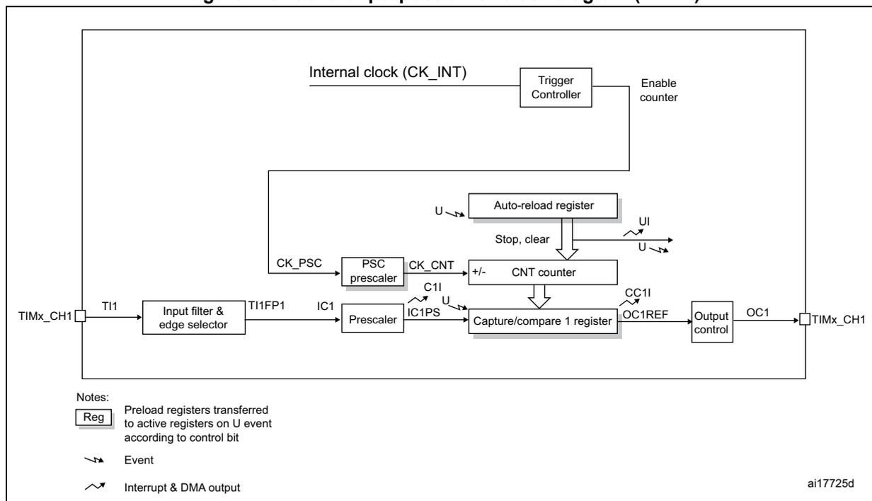
Figure 149. General-purpose timer block diagram (TIM14)
16.3 TIM14 functional description
16.3.1 Time-base unit
The main block of the programmable general-purpose timer is a 16-bit upcounter with its related auto-reload register. The counter clock can be divided by a prescaler.
The counter, the auto-reload register and the prescaler register can be written or read by software. This is true even when the counter is running.
The time-base unit includes:
- • Counter register (TIMx_CNT)
- • Prescaler register (TIMx_PSC)
- • Auto-reload register (TIMx_ARR)
The auto-reload register is preloaded. Writing to or reading from the auto-reload register accesses the preload register. The content of the preload register are transferred into the shadow register permanently or at each update event (UEV), depending on the auto-reload preload enable bit (ARPE) in TIMx_CR1 register. The update event is sent when the counter reaches the overflow and if the UDIS bit equals 0 in the TIMx_CR1 register. It can also be generated by software. The generation of the update event is described in detailed for each configuration.
The counter is clocked by the prescaler output CK_CNT, which is enabled only when the counter enable bit (CEN) in TIMx_CR1 register is set (refer also to the slave mode controller description to get more details on counter enabling).
Note that the counter starts counting 1 clock cycle after setting the CEN bit in the TIMx_CR1 register.
Prescaler description
The prescaler can divide the counter clock frequency by any factor between 1 and 65536. It is based on a 16-bit counter controlled through a 16-bit register (in the TIMx_PSC register). It can be changed on the fly as this control register is buffered. The new prescaler ratio is taken into account at the next update event.
Figure 151 and Figure 152 give some examples of the counter behavior when the prescaler ratio is changed on the fly.
Figure 150. Counter timing diagram with prescaler division change from 1 to 2
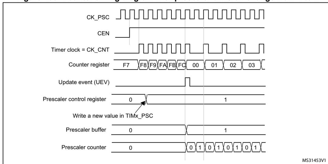
The diagram illustrates the timing of a timer when the prescaler division is changed from 1 to 2. The top signal is CK_PSC, a periodic clock. Below it is CEN, which goes high to enable the timer. The timer clock (CK_CNT) is derived from CK_PSC. The counter register shows values F7, F8, F9, FA, FB, FC, 00, 01, 02, 03. An update event (UEV) occurs after the counter reaches FC. At this UEV, the prescaler control register is updated from 0 to 1. The prescaler buffer also updates from 0 to 1. The prescaler counter, which counts up to 1 (division of 2), then begins counting 0, 1, 0, 1, 0, 1, 0, 1.
Figure 151. Counter timing diagram with prescaler division change from 1 to 4
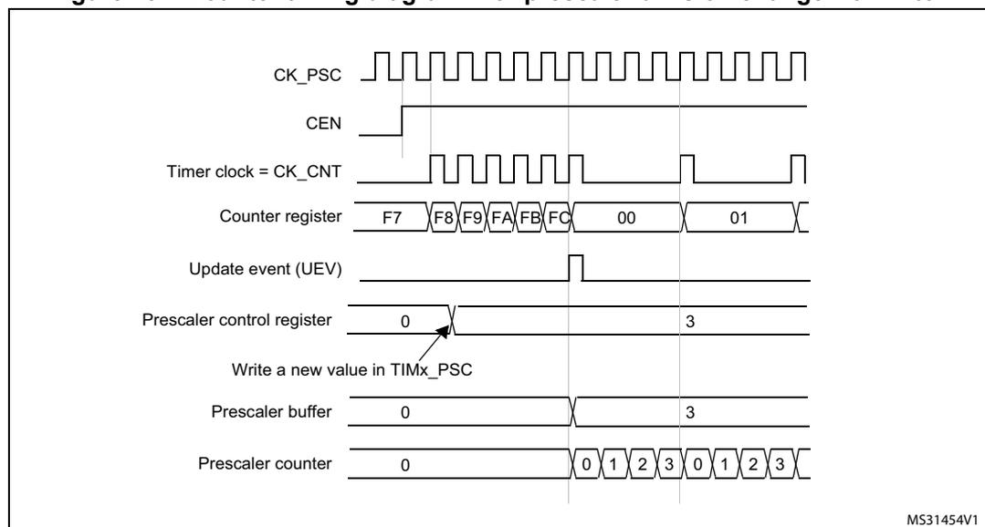
The diagram illustrates the timing of a timer when the prescaler division is changed from 1 to 4. The top signal is CK_PSC, a periodic clock. Below it is CEN, which goes high to enable the timer. The timer clock (CK_CNT) is derived from CK_PSC. The counter register shows values F7, F8, F9, FA, FB, FC, 00, 01. An update event (UEV) occurs after the counter reaches FC. At this UEV, the prescaler control register is updated from 0 to 3 (division of 4). The prescaler buffer also updates from 0 to 3. The prescaler counter, which counts up to 3 (division of 4), then begins counting 0, 1, 2, 3, 0, 1, 2, 3.
16.3.2 Counter operation
The counter counts from 0 to the auto-reload value (content of the TIMx_ARR register), then restarts from 0 and generates a counter overflow event.
Setting the UG bit in the TIMx_EGR register also generates an update event.
The UEV event can be disabled by software by setting the UDIS bit in the TIMx_CR1 register. This is to avoid updating the shadow registers while writing new values in the preload registers. Then no update event occurs until the UDIS bit has been written to 0. However, the counter restarts from 0, as well as the counter of the prescaler (but the prescale rate does not change). In addition, if the URS bit (update request selection) in TIMx_CR1 register is set, setting the UG bit generates an update event UEV but without setting the UIF flag (thus no interrupt is sent). This is to avoid generating both update and capture interrupts when clearing the counter on the capture event.
When an update event occurs, all the registers are updated and the update flag (UIF bit in TIMx_SR register) is set (depending on the URS bit):
- • The auto-reload shadow register is updated with the preload value (TIMx_ARR),
- • The buffer of the prescaler is reloaded with the preload value (content of the TIMx_PSC register).
The following figures show some examples of the counter behavior for different clock frequencies when TIMx_ARR=0x36.
Figure 152. Counter timing diagram, internal clock divided by 1
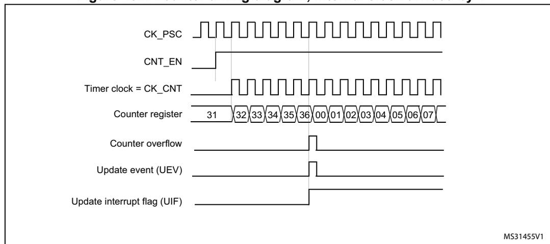
Timing diagram showing the counter behavior when the internal clock is divided by 1. The diagram includes the following signals and states:
- CK_PSC : Prescaler clock signal (square wave).
- CNT_EN : Counter enable signal (goes high to start counting).
- Timer clock = CK_CNT : Counter clock signal (square wave, same frequency as CK_PSC).
- Counter register : Shows the counter values: 31, 32, 33, 34, 35, 36, 00, 01, 02, 03, 04, 05, 06, 07. The values 32 through 36 are highlighted in yellow.
- Counter overflow : Pulse generated when the counter reaches 36 and rolls over to 00.
- Update event (UEV) : Pulse generated at the counter overflow.
- Update interrupt flag (UIF) : Flag set at the counter overflow.
MS31455V1
Figure 153. Counter timing diagram, internal clock divided by 2
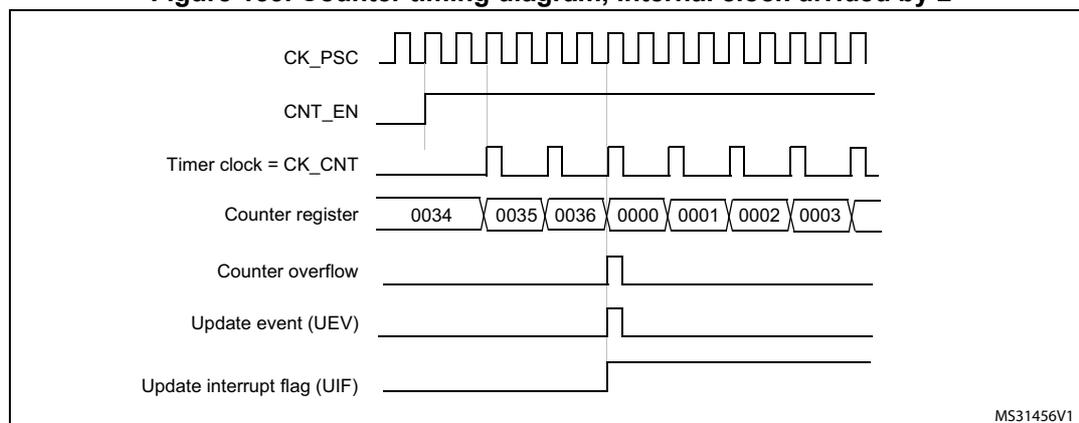
Timing diagram showing the counter behavior when the internal clock is divided by 2. The diagram includes the following signals and states:
- CK_PSC : Prescaler clock signal (square wave).
- CNT_EN : Counter enable signal (goes high to start counting).
- Timer clock = CK_CNT : Counter clock signal (square wave, half the frequency of CK_PSC).
- Counter register : Shows the counter values: 0034, 0035, 0036, 0000, 0001, 0002, 0003. The values 0034 through 0036 are highlighted in yellow.
- Counter overflow : Pulse generated when the counter reaches 0036 and rolls over to 0000.
- Update event (UEV) : Pulse generated at the counter overflow.
- Update interrupt flag (UIF) : Flag set at the counter overflow.
MS31456V1
Figure 154. Counter timing diagram, internal clock divided by 4
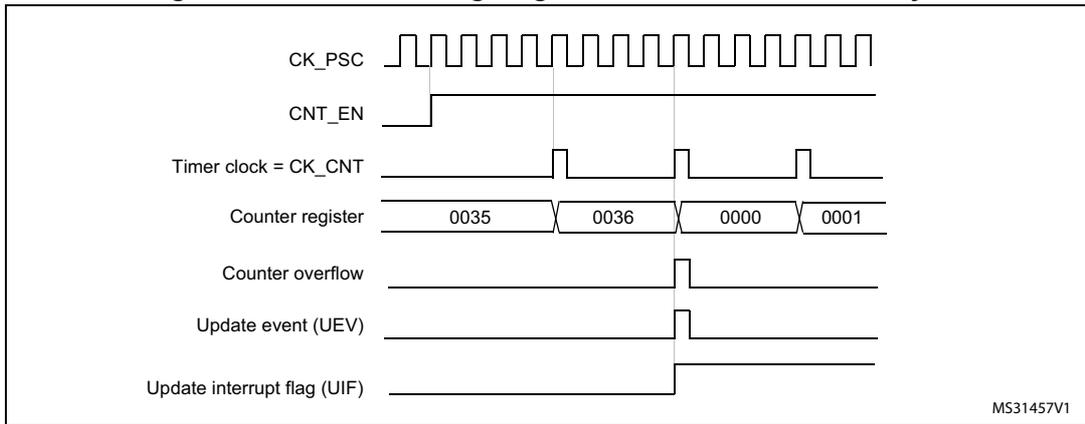
Timing diagram for internal clock divided by 4. The diagram shows the relationship between the prescaler clock (CK_PSC), counter enable (CNT_EN), timer clock (CK_CNT), counter register values, counter overflow, update event (UEV), and update interrupt flag (UIF). The counter register values shown are 0035, 0036, 0000, and 0001. The counter overflow occurs when the counter reaches 0036. The update event (UEV) and update interrupt flag (UIF) are generated when the counter reaches 0000.
MS31457V1
Figure 155. Counter timing diagram, internal clock divided by N
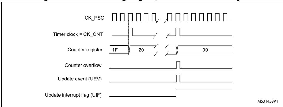
Timing diagram for internal clock divided by N. The diagram shows the relationship between the prescaler clock (CK_PSC), timer clock (CK_CNT), counter register values, counter overflow, update event (UEV), and update interrupt flag (UIF). The counter register values shown are 1F, 20, and 00. The counter overflow occurs when the counter reaches 20. The update event (UEV) and update interrupt flag (UIF) are generated when the counter reaches 00.
MS31458V1
Figure 156. Counter timing diagram, update event when ARPE=0 (TIMx_ARR not preloaded)
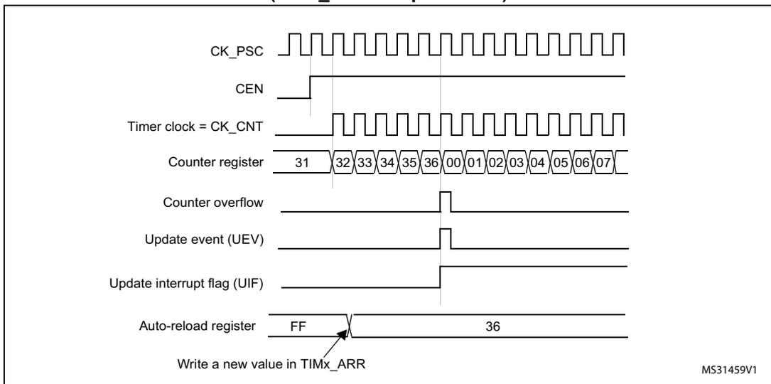
Timing diagram for update event when ARPE=0 (TIMx_ARR not preloaded). The diagram shows the relationship between the prescaler clock (CK_PSC), counter enable (CEN), timer clock (CK_CNT), counter register values, counter overflow, update event (UEV), update interrupt flag (UIF), and auto-reload register (ARR). The counter register values shown are 31, 32, 33, 34, 35, 36, 00, 01, 02, 03, 04, 05, 06, and 07. The counter overflow occurs when the counter reaches 36. The update event (UEV) and update interrupt flag (UIF) are generated when the counter reaches 00. The auto-reload register (ARR) is shown with values FF and 36. An arrow points to the value 36 in the ARR, indicating that a new value can be written to TIMx_ARR.
MS31459V1
Figure 157. Counter timing diagram, update event when ARPE=1 (TIMx_ARR preloaded)
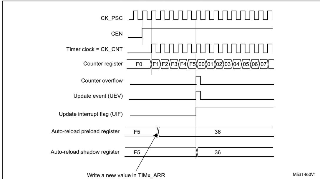
The diagram shows the following signals and their timing:
- CK_PSC: A periodic square wave clock signal.
- CEN: Counter Enable signal, which goes high to enable the counter.
- Timer clock = CK_CNT: The clock signal for the counter, derived from CK_PSC.
- Counter register: Shows the count values: F0, F1, F2, F3, F4, F5, 00, 01, 02, 03, 04, 05, 06, 07. An arrow indicates a write to TIMx_ARR.
- Counter overflow: A pulse when the counter reaches its maximum value (00).
- Update event (UEV): A pulse generated when the counter overflows and ARPE=1.
- Update interrupt flag (UIF): A flag that is set when an update event occurs.
- Auto-reload preload register: Shows the value F5 being updated to 36.
- Auto-reload shadow register: Shows the value F5 being updated to 36.
MS31460V1
16.3.3 Clock source
The counter clock is provided by the Internal clock (CK_INT) source.
The CEN (in the TIMx_CR1 register) and UG bits (in the TIMx_EGR register) are actual control bits and can be changed only by software (except for UG that remains cleared automatically). As soon as the CEN bit is written to 1, the prescaler is clocked by the internal clock CK_INT.
Figure 158 shows the behavior of the control circuit and the upcounter in normal mode, without prescaler.
Figure 158. Control circuit in normal mode, internal clock divided by 1
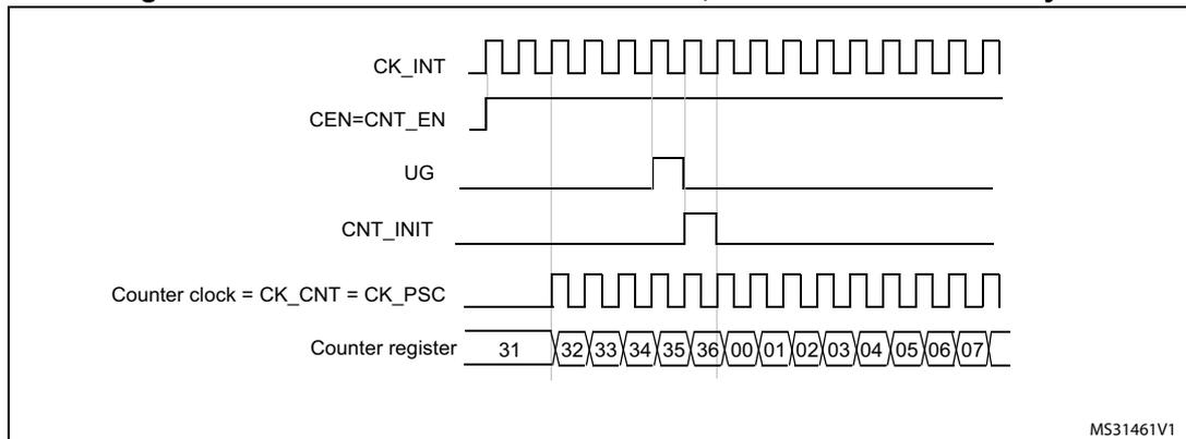
The diagram shows the following signals and their timing:
- CK_INT: The internal clock signal.
- CEN=CNT_EN: Counter Enable signal, which goes high to enable the counter.
- UG: Update Generation bit, which is set to generate an update event.
- CNT_INIT: Counter Initialization signal, which is set to initialize the counter.
- Counter clock = CK_CNT = CK_PSC: The clock signal for the counter, which is the internal clock divided by 1.
- Counter register: Shows the count values: 31, 32, 33, 34, 35, 36, 00, 01, 02, 03, 04, 05, 06, 07.
MS31461V1
16.3.4 Capture/compare channels
Each Capture/Compare channel is built around a capture/compare register (including a shadow register), a input stage for capture (with digital filter, multiplexing and prescaler) and an output stage (with comparator and output control).
Figure 159 to Figure 161 give an overview of one capture/compare channel.
The input stage samples the corresponding TIx input to generate a filtered signal TIxF. Then, an edge detector with polarity selection generates a signal (TIxFPx) which can be used as trigger input by the slave mode controller or as the capture command. It is prescaled before the capture register (ICxPS).
Figure 159. Capture/compare channel (example: channel 1 input stage)
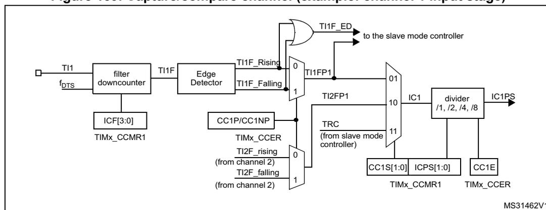
This block diagram illustrates the input stage of a capture/compare channel. The input signal TI1 is processed through a filter downcounter (controlled by ICF[3:0] and TIMx_CCMR1) to produce a filtered signal TI1F. This signal is then passed to an Edge Detector (controlled by CC1P/CC1NP and TIMx_CCER) which generates rising (TI1F_Rising) and falling (TI1F_Falling) edge signals. These signals are combined via an OR gate to produce TI1F_ED, which is sent to the slave mode controller. The edge signals are also multiplexed (01) to produce TI1FP1. This signal is further processed by a second multiplexer (10) along with TRC (from slave mode controller) to produce IC1. IC1 is then divided by a divider (/1, /2, /4, /8) to produce IC1PS. The divider is controlled by CC1S[1:0], ICPS[1:0], and CC1E (TIMx_CCER). The diagram also shows various control signals and registers: ICF[3:0], TIMx_CCMR1, CC1P/CC1NP, TIMx_CCER, TRC, CC1S[1:0], ICPS[1:0], CC1E, and MS31462V1.
The output stage generates an intermediate waveform which is then used for reference: OCxRef (active high). The polarity acts at the end of the chain.
Figure 160. Capture/compare channel 1 main circuit
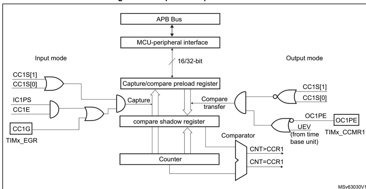
This block diagram shows the main circuit of a capture/compare channel. It is divided into Input mode and Output mode. In Input mode, the CC1S[1] and CC1S[0] signals are ORed and then ANDed with the output of an OR gate combining IC1PS and CC1E. This result is ANDed with CC1G (TIMx_EGR) to control the Capture operation. In Output mode, the CC1S[1] and CC1S[0] signals are ORed and then ANDed with the output of an OR gate combining OC1PE and UEV (from time base unit). This result is ANDed with CC1G (TIMx_EGR) to control the Compare transfer operation. The Capture/compare preload register and compare shadow register are connected to the APB Bus via the MCU-peripheral interface. The Counter is connected to the compare shadow register and the Comparator. The Comparator outputs CNT>CCR1 and CNT=CCR1. The diagram also shows the APB Bus, MCU-peripheral interface, 16/32-bit bus, Capture/compare preload register, compare shadow register, Counter, Comparator, and MSv63030V1.
Figure 161. Output stage of capture/compare channel (channel 1)
![Figure 161. Output stage of capture/compare channel (channel 1). The diagram shows the internal logic of the output stage. On the left, two inputs, 'CNT > CCR2' and 'CNT = CCR2', are connected to an 'Output mode controller'. This controller is also connected to a register 'OC2M[2:0]' in 'TIMx_CCMR1'. The controller outputs 'OC1_REF'. This signal is connected to a multiplexer and also to 'The master mode controller'. The multiplexer has two inputs: '0' (direct connection) and '1' (inverted connection via a NOT gate). The multiplexer is controlled by 'CC1P' in 'TIMx_CCER'. The output of the multiplexer is connected to an 'Output enable circuit', which is controlled by 'CC1E' in 'TIMx_CCER'. The final output is 'OC1'.](/RM0360-STM32F030x4-x6-x8-xC-070x6-xB/fb0319c4dcc4ab3fe727d783a67a355a_img.jpg)
The capture/compare block is made of one preload register and one shadow register. Write and read always access the preload register.
In capture mode, captures are actually done in the shadow register, which is copied into the preload register.
In compare mode, the content of the preload register is copied into the shadow register which is compared to the counter.
16.3.5 Input capture mode
In Input capture mode, the Capture/Compare Registers (TIMx_CCRx) are used to latch the value of the counter after a transition detected by the corresponding ICx signal. When a capture occurs, the corresponding CCXIF flag (TIMx_SR register) is set and an interrupt or a DMA request can be sent if they are enabled. If a capture occurs while the CCXIF flag was already high, then the over-capture flag CCxOF (TIMx_SR register) is set. CCxIF can be cleared by software by writing it to '0' or by reading the captured data stored in the TIMx_CCRx register. CCxOF is cleared when it is written with 0.
The following example shows how to capture the counter value in TIMx_CCR1 when TI1 input rises. To do this, use the following procedure:
- 1. Select the active input: TIMx_CCR1 must be linked to the TI1 input, so write the CC1S bits to '01' in the TIMx_CCMR1 register. As soon as CC1S becomes different from '00', the channel is configured in input mode and the TIMx_CCR1 register becomes read-only.
- 2. Program the appropriate input filter duration in relation with the signal connected to the timer (when the input is one of the TIx (ICxF bits in the TIMx_CCMRx register). Let us imagine that, when toggling, the input signal is not stable during at most 5 internal clock cycles. We must program a filter duration longer than these 5 clock cycles. We can validate a transition on TI1 when 8 consecutive samples with the new level have been
detected (sampled at \( f_{DTS} \) frequency). Then write IC1F bits to '0011' in the TIMx_CCMR1 register.
- 3. Select the edge of the active transition on the TI1 channel by programming CC1P and CC1NP bits to '00' in the TIMx_CCER register (rising edge in this case).
- 4. Program the input prescaler. In our example, we wish the capture to be performed at each valid transition, so the prescaler is disabled (write IC1PS bits to '00' in the TIMx_CCMR1 register).
- 5. Enable capture from the counter into the capture register by setting the CC1E bit in the TIMx_CCER register.
- 6. If needed, enable the related interrupt request by setting the CC1IE bit in the TIMx_DIER register.
For code example refer to the Appendix section A.8.3: Input capture configuration .
When an input capture occurs:
- • The TIMx_CCR1 register gets the value of the counter on the active transition.
- • CC1IF flag is set (interrupt flag). CC1OF is also set if at least two consecutive captures occurred whereas the flag was not cleared.
- • An interrupt is generated depending on the CC1IE bit.
For code example refer to the Appendix section A.8.4: Input capture data management .
In order to handle the overcapture, it is recommended to read the data before the overcapture flag. This is to avoid missing an overcapture which could happen after reading the flag and before reading the data.
Note: IC interrupt requests can be generated by software by setting the CCxG bit in the TIMx_EGR register.
16.3.6 Forced output mode
In output mode (CCxS bits = '00' in the TIMx_CCMRx register), each output compare signal (OCxREF and then OCx) can be forced to active or inactive level directly by software, independently of any comparison between the output compare register and the counter.
To force an output compare signal (OCXREF/OCx) to its active level, one just needs to write '101' in the OCxM bits in the corresponding TIMx_CCMRx register. Thus OCXREF is forced high (OCxREF is always active high) and OCx get opposite value to CCxP polarity bit.
For example: CCxP='0' (OCx active high) => OCx is forced to high level.
The OCxREF signal can be forced low by writing the OCxM bits to '100' in the TIMx_CCMRx register.
The comparison between the TIMx_CCRx shadow register and the counter is still performed and allows the flag to be set. Interrupt requests can be sent accordingly. This is described in the output compare mode section below.
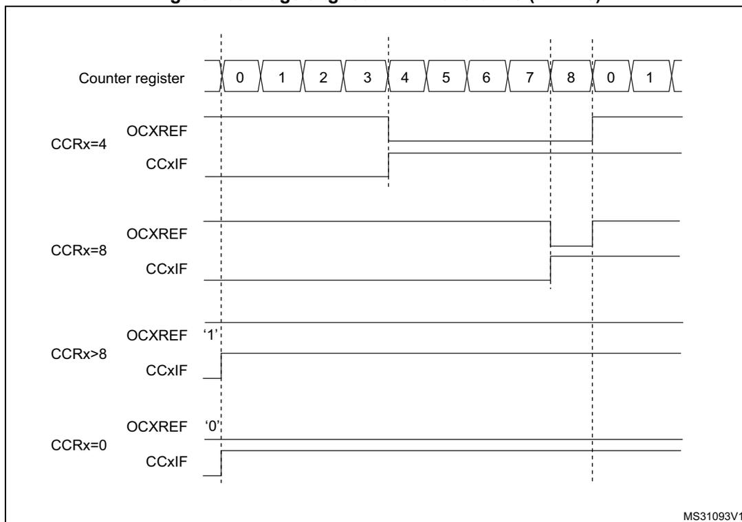
16.3.7 Output compare mode
This function is used to control an output waveform or to indicate when a period of time has elapsed.
When a match is found between the capture/compare register and the counter, the output compare function:
- 1. Assigns the corresponding output pin to a programmable value defined by the output compare mode (OCxM bits in the TIMx_CCMRx register) and the output polarity (CCxP bit in the TIMx_CCER register). The output pin can keep its level (OCxM='000'), be set active (OCxM='001'), be set inactive (OCxM='010') or can toggle (OCxM='011') on match.
- 2. Sets a flag in the interrupt status register (CCxIF bit in the TIMx_SR register).
- 3. Generates an interrupt if the corresponding interrupt mask is set (CCxIE bit in the TIMx_DIER register).
The TIMx_CCRx registers can be programmed with or without preload registers using the OCxPE bit in the TIMx_CCMRx register.
In output compare mode, the update event UEV has no effect on OCxREF and OCx output. The timing resolution is one count of the counter. Output compare mode can also be used to output a single pulse (in One-pulse mode).
Procedure:
- 1. Select the counter clock (internal, external, prescaler).
- 2. Write the desired data in the TIMx_ARR and TIMx_CCRx registers.
- 3. Set the CCxIE bit if an interrupt request is to be generated.
- 4. Select the output mode. For example:
- – Write OCxM = '011' to toggle OCx output pin when CNT matches CCRx
- – Write OCxPE = '0' to disable preload register
- – Write CCxP = '0' to select active high polarity
- – Write CCxE = '1' to enable the output
- 5. Enable the counter by setting the CEN bit in the TIMx_CR1 register.
For code example refer to the Appendix section A.8.7: Output compare configuration .
The TIMx_CCRx register can be updated at any time by software to control the output waveform, provided that the preload register is not enabled (OCxPE='0', else TIMx_CCRx shadow register is updated only at the next update event UEV). An example is given in Figure 162 .
Figure 162. Output compare mode, toggle on OC1
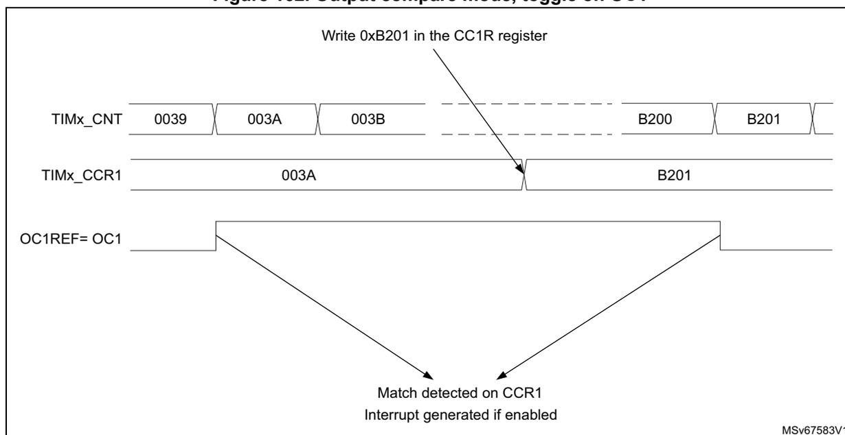
Write 0xB201 in the CC1R register
TIMx_CNT: 0039 | 003A | 003B | ... | B200 | B201
TIMx_CCR1: 003A | B201
OC1REF= OC1: [Signal line showing state changes at match points]
Match detected on CCR1
Interrupt generated if enabled
MSV67583V1
16.3.8 PWM mode
Pulse Width Modulation mode allows to generate a signal with a frequency determined by the value of the TIMx_ARR register and a duty cycle determined by the value of the TIMx_CCRx register.
The PWM mode can be selected independently on each channel (one PWM per OCx output) by writing '110' (PWM mode 1) or '111' (PWM mode 2) in the OCxM bits in the TIMx_CCMRx register. The corresponding preload register must be enabled by setting the OCxPE bit in the TIMx_CCMRx register, and eventually the auto-reload preload register by setting the ARPE bit in the TIMx_CR1 register.
As the preload registers are transferred to the shadow registers only when an update event occurs, before starting the counter, all registers must be initialized by setting the UG bit in the TIMx_EGR register.
The OCx polarity is software programmable using the CCxP bit in the TIMx_CCER register. It can be programmed as active high or active low. The OCx output is enabled by the CCxE bit in the TIMx_CCER register. Refer to the TIMx_CCERx register description for more details.
In PWM mode (1 or 2), TIMx_CNT and TIMx_CCRx are always compared to determine whether \( TIMx\_CNT \leq TIMx\_CCRx \) .
The timer is able to generate PWM in edge-aligned mode only since the counter is upcounting.
PWM edge-aligned mode
In the following example, we consider PWM mode 1. The reference PWM signal OCxREF is high as long as \( TIMx\_CNT < TIMx\_CCRx \) else it becomes low. If the compare value in TIMx_CCRx is greater than the auto-reload value (in TIMx_ARR) then OCxREF is held at '1'. If the compare value is 0 then OCxRef is held at '0'. Figure 163 shows some edge-aligned PWM waveforms in an example where TIMx_ARR=8.
Figure 163. Edge-aligned PWM waveforms (ARR=8)
For code example refer to the Appendix section A.8.8: Edge-aligned PWM configuration example .
16.3.9 Debug mode
When the microcontroller enters debug mode (Cortex™-M0 core halted), the TIMx counter either continues to work normally or stops, depending on DBG_TIMx_STOP configuration bit in DBG module.
16.4 TIM14 registers
16.4.1 TIM14 control register 1 (TIM14_CR1)
Address offset: 0x00
Reset value: 0x0000
| 15 | 14 | 13 | 12 | 11 | 10 | 9 | 8 | 7 | 6 | 5 | 4 | 3 | 2 | 1 | 0 |
|---|---|---|---|---|---|---|---|---|---|---|---|---|---|---|---|
| Res. | Res. | Res. | Res. | Res. | Res. | CKD[1:0] | ARPE | Res. | Res. | Res. | Res. | URS | UDIS | CEN | |
| rw | rw | rw | rw | rw | |||||||||||
Bits 15:10 Reserved, must be kept at reset value.
Bits 9:8 CKD[1:0] : Clock division
This bit-field indicates the division ratio between the timer clock (CK_INT) frequency and sampling clock used by the digital filters (ETR, TIx),
00: \( t_{DTS} = t_{CK\_INT} \)
01: \( t_{DTS} = 2 \times t_{CK\_INT} \)
10: \( t_{DTS} = 4 \times t_{CK\_INT} \)
11: Reserved
Bit 7 ARPE : Auto-reload preload enable
0: TIMx_ARR register is not buffered
1: TIMx_ARR register is buffered
Bits 6:3 Reserved, must be kept at reset value.
Bit 2 URS : Update request source
This bit is set and cleared by software to select the update interrupt (UEV) sources.
0: Any of the following events generate an UEV if enabled:
- – Counter overflow
- – Setting the UG bit
1: Only counter overflow generates an UEV if enabled.
Bit 1 UDIS : Update disable
This bit is set and cleared by software to enable/disable update interrupt (UEV) event generation.
0: UEV enabled. An UEV is generated by one of the following events:
- – Counter overflow
- – Setting the UG bit.
Buffered registers are then loaded with their preload values.
1: UEV disabled. No UEV is generated, shadow registers keep their value (ARR, PSC, CCRx). The counter and the prescaler are reinitialized if the UG bit is set.
Bit 0 CEN : Counter enable
0: Counter disabled
1: Counter enabled
16.4.2 TIM14 interrupt enable register (TIM14_DIER)
Address offset: 0x0C
Reset value: 0x0000
| 15 | 14 | 13 | 12 | 11 | 10 | 9 | 8 | 7 | 6 | 5 | 4 | 3 | 2 | 1 | 0 |
|---|---|---|---|---|---|---|---|---|---|---|---|---|---|---|---|
| Res. | Res. | Res. | Res. | Res. | Res. | Res. | Res. | Res. | Res. | Res. | Res. | Res. | Res. | CC1IE | UIE |
| rw | rw |
Bits 15:2 Reserved, must be kept at reset value.
Bit 1 CC1IE : Capture/Compare 1 interrupt enable
0: CC1 interrupt disabled
1: CC1 interrupt enabled
Bit 0 UIE : Update interrupt enable
0: Update interrupt disabled
1: Update interrupt enabled
16.4.3 TIM14 status register (TIM14_SR)
Address offset: 0x10
Reset value: 0x0000
| 15 | 14 | 13 | 12 | 11 | 10 | 9 | 8 | 7 | 6 | 5 | 4 | 3 | 2 | 1 | 0 |
|---|---|---|---|---|---|---|---|---|---|---|---|---|---|---|---|
| Res. | Res. | Res. | Res. | Res. | Res. | CC1OF | Res. | Res. | Res. | Res. | Res. | Res. | Res. | CC1IF | UIF |
| rc_w0 | rc_w0 | rc_w0 |
Bits 15:10 Reserved, must be kept at reset value.
Bit 9 CC1OF : Capture/Compare 1 overcapture flag
This flag is set by hardware only when the corresponding channel is configured in input capture mode. It is cleared by software by writing it to '0'.
0: No overcapture has been detected.
1: The counter value has been captured in TIMx_CCR1 register while CC1IF flag was already set
Bits 8:2 Reserved, must be kept at reset value.
Bit 1 CC1IF : Capture/compare 1 interrupt flag
Condtion: channel CC1 is configured as output
This flag is set by hardware when the counter matches the compare value. It is cleared by software.
0: No match.
1: The content of the counter TIMx_CNT matches the content of the TIMx_CCR1 register. When the contents of TIMx_CCR1 are greater than the contents of TIMx_ARR, the CC1IF bit goes high on the counter overflow.
Condition: channel CC1 is configured as input
This bit is set by hardware on a capture. It is cleared by software or by reading the TIMx_CCR1 register.
0: No input capture occurred.
1: The counter value has been captured in TIMx_CCR1 register (an edge has been detected on IC1 which matches the selected polarity).
Bit 0 UIF : Update interrupt flag
This bit is set by hardware on an update event. It is cleared by software.
0: No update occurred.
1: Update interrupt pending. This bit is set by hardware when the registers are updated:
- – At overflow and if UDIS='0' in the TIMx_CR1 register.
- – When CNT is reinitialized by software using the UG bit in TIMx_EGR register, if URS='0' and UDIS='0' in the TIMx_CR1 register.
16.4.4 TIM14 event generation register (TIM14_EGR)
Address offset: 0x14
Reset value: 0x0000
| 15 | 14 | 13 | 12 | 11 | 10 | 9 | 8 | 7 | 6 | 5 | 4 | 3 | 2 | 1 | 0 |
|---|---|---|---|---|---|---|---|---|---|---|---|---|---|---|---|
| Res. | Res. | Res. | Res. | Res. | Res. | Res. | Res. | Res. | Res. | Res. | Res. | Res. | Res. | CC1G | UG |
| w | w |
Bits 15:2 Reserved, must be kept at reset value.
Bit 1 CC1G : Capture/compare 1 generation
This bit is set by software in order to generate an event, it is automatically cleared by hardware.
0: No action
1: A capture/compare event is generated on channel 1:
Condition: channel CC1 is configured as output
CC1IF flag is set, Corresponding interrupt or is sent if enabled.
Condition: channel CC1 is configured as input
The current value of the counter is captured in TIMx_CCR1 register. The CC1IF flag is set, the corresponding interrupt is sent if enabled. The CC1OF flag is set if the CC1IF flag was already high.
Bit 0 UG : Update generation
This bit can be set by software, it is automatically cleared by hardware.
0: No action
1: Re-initialize the counter and generates an update of the registers. Note that the prescaler counter is cleared too (anyway the prescaler ratio is not affected). The counter is cleared.
16.4.5 TIM14 capture/compare mode register 1 [alternate] (TIM14_CCMR1)
Address offset: 0x18
Reset value: 0x0000
The same register can be used for input capture mode (this section) or for output compare mode (next section).. The direction of a channel is defined by configuring the corresponding CCxS bits. All the other bits of this register have a different function in input and in output mode. For a given bit, OCxx describes its function when the channel is configured in output, ICxx describes its function when the channel is configured in input. So one must take care that the same bit can have a different meaning for the input stage and for the output stage
| 15 | 14 | 13 | 12 | 11 | 10 | 9 | 8 | 7 | 6 | 5 | 4 | 3 | 2 | 1 | 0 |
|---|---|---|---|---|---|---|---|---|---|---|---|---|---|---|---|
| Res. | Res. | Res. | Res. | Res. | Res. | Res. | Res. | IC1F[3:0] | IC1PSC[1:0] | CC1S[1:0] | |||||
| rw | rw | rw | rw | rw | rw | rw | rw | ||||||||
Bits 15:8 Reserved, must be kept at reset value.
Bits 7:4 IC1F[3:0] : Input capture 1 filterThis bit-field defines the frequency used to sample TI1 input and the length of the digital filter applied to TI1. The digital filter is made of an event counter in which N events are needed to validate a transition on the output:
- 0000: No filter, sampling is done at \( f_{DTS} \)
- 0001: \( f_{SAMPLING} = f_{CK\_INT} \) , N = 2
- 0010: \( f_{SAMPLING} = f_{CK\_INT} \) , N = 4
- 0011: \( f_{SAMPLING} = f_{CK\_INT} \) , N = 8
- 0100: \( f_{SAMPLING} = f_{DTS} / 2 \) , N = 6
- 0101: \( f_{SAMPLING} = f_{DTS} / 2 \) , N = 8
- 0110: \( f_{SAMPLING} = f_{DTS} / 4 \) , N = 6
- 0111: \( f_{SAMPLING} = f_{DTS} / 4 \) , N = 8
- 1000: \( f_{SAMPLING} = f_{DTS} / 8 \) , N = 6
- 1001: \( f_{SAMPLING} = f_{DTS} / 8 \) , N = 8
- 1010: \( f_{SAMPLING} = f_{DTS} / 16 \) , N = 5
- 1011: \( f_{SAMPLING} = f_{DTS} / 16 \) , N = 6
- 1100: \( f_{SAMPLING} = f_{DTS} / 16 \) , N = 8
- 1101: \( f_{SAMPLING} = f_{DTS} / 32 \) , N = 5
- 1110: \( f_{SAMPLING} = f_{DTS} / 32 \) , N = 6
- 1111: \( f_{SAMPLING} = f_{DTS} / 32 \) , N = 8
Note: Care must be taken that \( f_{DTS} \) is replaced in the formula by \( CK\_INT \) when \( ICxF[3:0] = 1, 2 \) or \( 3 \) .
Bits 3:2 IC1PSC[1:0] : Input capture 1 prescalerThis bit-field defines the ratio of the prescaler acting on CC1 input (IC1).
The prescaler is reset as soon as \( CC1E='0' \) (TIMx_CCER register).
- 00: no prescaler, capture is done each time an edge is detected on the capture input
- 01: capture is done once every 2 events
- 10: capture is done once every 4 events
- 11: capture is done once every 8 events
This bit-field defines the direction of the channel (input/output) as well as the used input.
- 00: CC1 channel is configured as output
- 01: CC1 channel is configured as input, IC1 is mapped on TI1
- Other: Reserved
Note: CC1S bits are writable only when the channel is OFF ( \( CC1E = 0 \) in TIMx_CCER).
16.4.6 TIM14 capture/compare mode register 1 [alternate] (TIM14_CCMR1)
Address offset: 0x18
Reset value: 0x0000
The same register can be used for output compare mode (this section) or for input capture mode (previous section). The direction of a channel is defined by configuring the corresponding CCxS bits. All the other bits of this register have a different function in input and in output mode. For a given bit, OCxx describes its function when the channel is configured in output, ICxx describes its function when the channel is configured in input. So one must take care that the same bit can have a different meaning for the input stage and for the output stage.
| 15 | 14 | 13 | 12 | 11 | 10 | 9 | 8 | 7 | 6 | 5 | 4 | 3 | 2 | 1 | 0 |
|---|---|---|---|---|---|---|---|---|---|---|---|---|---|---|---|
| Res. | Res. | Res. | Res. | Res. | Res. | Res. | Res. | Res. | OC1M[2:0] | OC1PE | OC1FE | CC1S[1:0] | |||
| rw | rw | rw | rw | rw | rw | rw | |||||||||
Bits 15:7 Reserved, must be kept at reset value.
Bits 6:4 OC1M[2:0] : Output compare 1 mode
These bits define the behavior of the output reference signal OC1REF from which OC1 is derived. OC1REF is active high whereas OC1 active level depends on CC1P bit.
000: Frozen. The comparison between the output compare register TIMx_CCR1 and the counter TIMx_CNT has no effect on the outputs.
001: Set channel 1 to active level on match. OC1REF signal is forced high when the counter TIMx_CNT matches the capture/compare register 1 (TIMx_CCR1).
010: Set channel 1 to inactive level on match. OC1REF signal is forced low when the counter TIMx_CNT matches the capture/compare register 1 (TIMx_CCR1).
011: Toggle - OC1REF toggles when TIMx_CNT = TIMx_CCR1.
100: Force inactive level - OC1REF is forced low.
101: Force active level - OC1REF is forced high.
110: PWM mode 1 - Channel 1 is active as long as TIMx_CNT < TIMx_CCR1 else inactive.
111: PWM mode 2 - Channel 1 is inactive as long as TIMx_CNT < TIMx_CCR1 else active.
Note: In PWM mode 1 or 2, the OCREF level changes when the result of the comparison changes or when the output compare mode switches from frozen to PWM mode.
Bit 3 OC1PE : Output compare 1 preload enable
0: Preload register on TIMx_CCR1 disabled. TIMx_CCR1 can be written at anytime, the new value is taken in account immediately.
1: Preload register on TIMx_CCR1 enabled. Read/Write operations access the preload register. TIMx_CCR1 preload value is loaded in the active register at each update event.
Note: The PWM mode can be used without validating the preload register only in one pulse mode (OPM bit set in TIMx_CR1 register). Else the behavior is not guaranteed.
Bit 2 OC1FE : Output compare 1 fast enable
This bit is used to accelerate the effect of an event on the trigger in input on the CC output.
0: CC1 behaves normally depending on counter and CCR1 values even when the trigger is ON. The minimum delay to activate CC1 output when an edge occurs on the trigger input is 5 clock cycles.
1: An active edge on the trigger input acts like a compare match on CC1 output. OC is then set to the compare level independently of the result of the comparison. Delay to sample the trigger input and to activate CC1 output is reduced to 3 clock cycles. OC1FE acts only if the channel is configured in PWM1 or PWM2 mode.
Bits 1:0 CC1S[1:0] : Capture/Compare 1 selection
This bit-field defines the direction of the channel (input/output) as well as the used input.
00: CC1 channel is configured as output.
01: CC1 channel is configured as input, IC1 is mapped on TI1.
10: Reserved
11: Reserved
Note: CC1S bits are writable only when the channel is OFF (CC1E = 0 in TIMx_CCER).
16.4.7 TIM14 capture/compare enable register (TIM14_CCER)
Address offset: 0x20
Reset value: 0x0000
| 15 | 14 | 13 | 12 | 11 | 10 | 9 | 8 | 7 | 6 | 5 | 4 | 3 | 2 | 1 | 0 |
|---|---|---|---|---|---|---|---|---|---|---|---|---|---|---|---|
| Res. | Res. | Res. | Res. | Res. | Res. | Res. | Res. | Res. | Res. | Res. | Res. | CC1NP | Res. | CC1P | CC1E |
| rw | rw | rw |
Bits 15:4 Reserved, must be kept at reset value.
Bit 3 CC1NP : Capture/Compare 1 complementary output Polarity.
CC1 channel configured as output: CC1NP must be kept cleared.
CC1 channel configured as input: CC1NP bit is used in conjunction with CC1P to define TI1FP1 polarity (refer to CC1P description).
Bit 2 Reserved, must be kept at reset value.
Bit 1 CC1P : Capture/Compare 1 output Polarity.
Condition: CC1 channel configured as output
0: OC1 active high
1: OC1 active low
Condition: CC1 channel configured as input
The CC1P bit selects TI1FP1 and TI2FP1 polarity for trigger or capture operations.
00: noninverted/rising edge
Circuit is sensitive to TI1FP1 rising edge (capture mode), TI1FP1 is not inverted.
01: inverted/falling edge
Circuit is sensitive to TI1FP1 falling edge (capture mode), TI1FP1 is inverted.
10: reserved, do not use this configuration.
11: noninverted/both edges
Circuit is sensitive to both TI1FP1 rising and falling edges (capture mode), TI1FP1 is not inverted.
Bit 0 CC1E : Capture/Compare 1 output enable.
Condition: CC1 channel configured as output:
0: Off - OC1 is not active
1: On - OC1 signal is output on the corresponding output pin
Condition: CC1 channel configured as input:
This bit determines if a capture of the counter value can actually be done into the input capture/compare register 1 (TIMx_CCR1) or not.
0: Capture disabled
1: Capture enabled
Table 52. Output control bit for standard OCx channels
| CCxE bit | OCx output state |
|---|---|
| 0 | Output Disabled (OCx='0', OCx_EN='0') |
| 1 | OCx=OCxREF + Polarity, OCx_EN='1' |
Note: The state of the external I/O pins connected to the standard OCx channels depends on the OCx channel state and the GPIO registers.
16.4.8 TIM14 counter (TIM14_CNT)
Address offset: 0x24
Reset value: 0x0000
| 15 | 14 | 13 | 12 | 11 | 10 | 9 | 8 | 7 | 6 | 5 | 4 | 3 | 2 | 1 | 0 |
|---|---|---|---|---|---|---|---|---|---|---|---|---|---|---|---|
| CNT[15:0] | |||||||||||||||
| rw | rw | rw | rw | rw | rw | rw | rw | rw | rw | rw | rw | rw | rw | rw | rw |
Bits 15:0 CNT[15:0] : Counter value
16.4.9 TIM14 prescaler (TIM14_PSC)
Address offset: 0x28
Reset value: 0x0000

| 15 | 14 | 13 | 12 | 11 | 10 | 9 | 8 | 7 | 6 | 5 | 4 | 3 | 2 | 1 | 0 |
| PSC[15:0] | |||||||||||||||
| rw | rw | rw | rw | rw | rw | rw | rw | rw | rw | rw | rw | rw | rw | rw | rw |
Bits 15:0 PSC[15:0] : Prescaler value
The counter clock frequency CK_CNT is equal to \( f_{CK\_PSC} / (PSC[15:0] + 1) \) .
PSC contains the value to be loaded in the active prescaler register at each update event.
16.4.10 TIM14 auto-reload register (TIM14_ARR)
Address offset: 0x2C
Reset value: 0xFFFF

| 15 | 14 | 13 | 12 | 11 | 10 | 9 | 8 | 7 | 6 | 5 | 4 | 3 | 2 | 1 | 0 |
| ARR[15:0] | |||||||||||||||
| rw | rw | rw | rw | rw | rw | rw | rw | rw | rw | rw | rw | rw | rw | rw | rw |
Bits 15:0 ARR[15:0] : Auto-reload value
ARR is the value to be loaded in the actual auto-reload register.
Refer to the Section 16.3.1: Time-base unit on page 381 for more details about ARR update and behavior.
The counter is blocked while the auto-reload value is null.
16.4.11 TIM14 capture/compare register 1 (TIM14_CCR1)
Address offset: 0x34
Reset value: 0x0000

| 15 | 14 | 13 | 12 | 11 | 10 | 9 | 8 | 7 | 6 | 5 | 4 | 3 | 2 | 1 | 0 |
| CCR1[15:0] | |||||||||||||||
| rw | rw | rw | rw | rw | rw | rw | rw | rw | rw | rw | rw | rw | rw | rw | rw |
Bits 15:0 CCR1[15:0] : Capture/Compare 1 value
Condition: channel CC1 is configured as output
CCR1 is the value to be loaded in the actual capture/compare 1 register (preload value).
It is loaded permanently if the preload feature is not selected in the TIMx_CCMR1 register (bit OC1PE). Else the preload value is copied in the active capture/compare 1 register when an update event occurs.
The active capture/compare register contains the value to be compared to the counter TIMx_CNT and signaled on OC1 output.
Condition: channel CC1 is configured as input
CCR1 is the counter value transferred by the last input capture 1 event (IC1).
16.4.12 TIM14 option register (TIM14_OR)
Address offset: 0x50
Reset value: 0x0000
| 15 | 14 | 13 | 12 | 11 | 10 | 9 | 8 | 7 | 6 | 5 | 4 | 3 | 2 | 1 | 0 |
|---|---|---|---|---|---|---|---|---|---|---|---|---|---|---|---|
| Res. | Res. | Res. | Res. | Res. | Res. | Res. | Res. | Res. | Res. | Res. | Res. | Res. | Res. | TI1_RMP[1:0] | |
| rw | rw | ||||||||||||||
Bits 15:2 Reserved, must be kept at reset value.
Bits 1:0 TI1_RMP[1:0] : Timer Input 1 remap
Set and cleared by software.
00: TIM14 Channel1 is connected to the GPIO. Refer to the alternate function mapping in the device datasheets.
01: TIM14 Channel1 is connected to the RTCCLK.
10: TIM14 Channel1 is connected to the HSE/32 Clock.
11: TIM14 Channel1 is connected to the microcontroller clock output (MCO), this selection is controlled by the MCO[2:0] bits of the Clock configuration register (RCC_CFGR) (see Section 7.4.2: Clock configuration register (RCC_CFGR) ).
16.4.13 TIM14 register map
TIM14 registers are mapped as 16-bit addressable registers as described in the table below:
Table 53. TIM14 register map and reset values
| Offset | Register | 31 | 30 | 29 | 28 | 27 | 26 | 25 | 24 | 23 | 22 | 21 | 20 | 19 | 18 | 17 | 16 | 15 | 14 | 13 | 12 | 11 | 10 | 9 | 8 | 7 | 6 | 5 | 4 | 3 | 2 | 1 | 0 | ||
|---|---|---|---|---|---|---|---|---|---|---|---|---|---|---|---|---|---|---|---|---|---|---|---|---|---|---|---|---|---|---|---|---|---|---|---|
| 0x00 | TIM14_CR1 | Res. | Res. | Res. | Res. | Res. | Res. | Res. | Res. | Res. | Res. | Res. | Res. | Res. | Res. | Res. | Res. | Res. | Res. | Res. | Res. | Res. | Res. | CKD [1:0] | ARPE | Res. | Res. | Res. | Res. | URS | UDIS | CEN | |||
| Reset value | 0 | 0 | 0 | 0 | 0 | 0 | |||||||||||||||||||||||||||||
| 0x08 | Reserved | Res. | |||||||||||||||||||||||||||||||||
| 0x0C | TIM14_DIER | Res. | Res. | Res. | Res. | Res. | Res. | Res. | Res. | Res. | Res. | Res. | Res. | Res. | Res. | Res. | Res. | Res. | Res. | Res. | Res. | Res. | Res. | Res. | Res. | Res. | Res. | Res. | Res. | Res. | Res. | Res. | CC1IE | UIE | |
| Reset value | 0 | 0 | |||||||||||||||||||||||||||||||||
| 0x10 | TIM14_SR | Res. | Res. | Res. | Res. | Res. | Res. | Res. | Res. | Res. | Res. | Res. | Res. | Res. | Res. | Res. | Res. | Res. | Res. | Res. | Res. | Res. | Res. | CC1OF | Res. | Res. | Res. | Res. | Res. | Res. | Res. | Res. | CC1IF | UIF | |
| Reset value | 0 | 0 | 0 | ||||||||||||||||||||||||||||||||
| 0x14 | TIM14_EGR | Res. | Res. | Res. | Res. | Res. | Res. | Res. | Res. | Res. | Res. | Res. | Res. | Res. | Res. | Res. | Res. | Res. | Res. | Res. | Res. | Res. | Res. | Res. | Res. | Res. | Res. | Res. | Res. | Res. | Res. | Res. | CC1G | UG | |
| Reset value | 0 | 0 | |||||||||||||||||||||||||||||||||
| 0x18 | TIM14_CCMR1 Output compare mode | Res. | Res. | Res. | Res. | Res. | Res. | Res. | Res. | Res. | Res. | Res. | Res. | Res. | Res. | Res. | Res. | Res. | Res. | Res. | Res. | Res. | Res. | Res. | Res. | Res. | OC1M [2:0] | OC1PE | OC1FE | CC1S [1:0] | |||||
| Reset value | 0 | 0 | 0 | 0 | 0 | 0 | 0 | ||||||||||||||||||||||||||||
| 0x18 | TIM14_CCMR1 Input capture mode | Res. | Res. | Res. | Res. | Res. | Res. | Res. | Res. | Res. | Res. | Res. | Res. | Res. | Res. | Res. | Res. | Res. | Res. | Res. | Res. | Res. | Res. | Res. | Res. | Res. | IC1F[3:0] | IC1PSC [1:0] | CC1S [1:0] | ||||||
| Reset value | 0 | 0 | 0 | 0 | 0 | 0 | 0 | ||||||||||||||||||||||||||||
| 0x1C | Reserved | Res. | Res. | Res. | Res. | Res. | Res. | Res. | Res. | Res. | Res. | Res. | Res. | Res. | Res. | Res. | Res. | Res. | Res. | Res. | Res. | Res. | Res. | Res. | Res. | Res. | Res. | Res. | Res. | Res. | Res. | Res. | Res. | Res. | Res. |
| Reset value | |||||||||||||||||||||||||||||||||||
Table 53. TIM14 register map and reset values (continued)
| Offset | Register | 31 | 30 | 29 | 28 | 27 | 26 | 25 | 24 | 23 | 22 | 21 | 20 | 19 | 18 | 17 | 16 | 15 | 14 | 13 | 12 | 11 | 10 | 9 | 8 | 7 | 6 | 5 | 4 | 3 | 2 | 1 | 0 | |
|---|---|---|---|---|---|---|---|---|---|---|---|---|---|---|---|---|---|---|---|---|---|---|---|---|---|---|---|---|---|---|---|---|---|---|
| 0x20 | TIM14_CCER | Res. | Res. | Res. | Res. | Res. | Res. | Res. | Res. | Res. | Res. | Res. | Res. | Res. | Res. | Res. | Res. | Res. | Res. | Res. | Res. | Res. | Res. | Res. | Res. | Res. | Res. | Res. | Res. | Res. | CC1NP | Res. | CC1P | CC1E |
| Reset value | 0 | 0 | 0 | |||||||||||||||||||||||||||||||
| 0x24 | TIM14_CNT | Res. | Res. | Res. | Res. | Res. | Res. | Res. | Res. | Res. | Res. | Res. | Res. | Res. | Res. | Res. | Res. | CNT[15:0] | ||||||||||||||||
| Reset value | 0 | 0 | 0 | 0 | 0 | 0 | 0 | 0 | 0 | 0 | 0 | 0 | 0 | 0 | 0 | |||||||||||||||||||
| 0x28 | TIM14_PSC | Res. | Res. | Res. | Res. | Res. | Res. | Res. | Res. | Res. | Res. | Res. | Res. | Res. | Res. | Res. | Res. | PSC[15:0] | ||||||||||||||||
| Reset value | 0 | 0 | 0 | 0 | 0 | 0 | 0 | 0 | 0 | 0 | 0 | 0 | 0 | 0 | 0 | |||||||||||||||||||
| 0x2C | TIM14_ARR | Res. | Res. | Res. | Res. | Res. | Res. | Res. | Res. | Res. | Res. | Res. | Res. | Res. | Res. | Res. | Res. | ARR[15:0] | ||||||||||||||||
| Reset value | 1 | 1 | 1 | 1 | 1 | 1 | 1 | 1 | 1 | 1 | 1 | 1 | 1 | 1 | 1 | |||||||||||||||||||
| 0x30 | Reserved | Res. | Res. | Res. | Res. | Res. | Res. | Res. | Res. | Res. | Res. | Res. | Res. | Res. | Res. | Res. | Res. | Res. | Res. | Res. | Res. | Res. | Res. | Res. | Res. | Res. | Res. | Res. | Res. | Res. | Res. | Res. | Res. | |
| Reset value | ||||||||||||||||||||||||||||||||||
| 0x34 | TIM14_CCR1 | Res. | Res. | Res. | Res. | Res. | Res. | Res. | Res. | Res. | Res. | Res. | Res. | Res. | Res. | Res. | Res. | CCR1[15:0] | ||||||||||||||||
| Reset value | 0 | 0 | 0 | 0 | 0 | 0 | 0 | 0 | 0 | 0 | 0 | 0 | 0 | 0 | 0 | |||||||||||||||||||
| 0x38 to 0x4C | Reserved | Res. | Res. | Res. | Res. | Res. | Res. | Res. | Res. | Res. | Res. | Res. | Res. | Res. | Res. | Res. | Res. | Res. | Res. | Res. | Res. | Res. | Res. | Res. | Res. | Res. | Res. | Res. | Res. | Res. | Res. | Res. | Res. | |
| Reset value | ||||||||||||||||||||||||||||||||||
| 0x50 | TIM14_OR | Res. | Res. | Res. | Res. | Res. | Res. | Res. | Res. | Res. | Res. | Res. | Res. | Res. | Res. | Res. | Res. | Res. | Res. | Res. | Res. | Res. | Res. | Res. | Res. | Res. | Res. | Res. | Res. | Res. | Res. | Res. | TI1_RMP | |
| Reset value | 0 | |||||||||||||||||||||||||||||||||