4. Option bytes
There are up to 8 option bytes. They are configured by the end user depending on the application requirements. As a configuration example, the watchdog may be selected in hardware or software mode.
A 32-bit word is split up as follows in the option byte.
Table 10. Option byte format
| 31-24 | 23-16 | 15 -8 | 7-0 |
|---|---|---|---|
| Complemented option byte 1 | Option byte 1 | Complemented option byte 0 | Option byte 0 |
The organization of these bytes inside the information block is as shown in Table 11 .
The option byte can be read from the memory locations listed in Table 11 or from the Option byte register (FLASH_OBR).
Note: The new programmed option byte (user, read/write protection) are not loaded after a system reset. To reload them, either a POR or setting to '1' the OBL_LAUNCH bit is necessary.
Table 11. Option byte organization
| Address | [31:24] | [23:16] | [15:8] | [7:0] |
|---|---|---|---|---|
| 0x1FFF F800 | nUSER | USER | nRDP | RDP |
| 0x1FFF F804 | nData1 | Data1 | nData0 | Data0 |
| 0x1FFF F808 | nWRP1 | WRP1 | nWRP0 | WRP0 |
| 0x1FFF F80C | nWRP3 | WRP3 | nWRP2 | WRP2 |
On every power-on reset, the option byte loader (OBL) reads the information block and stores the data into the option byte register (FLASH_OBR) and the write protection register (FLASH_WRPR). During option byte loading, the bit-wise complementarity of the option byte and its corresponding complemented option byte is verified. In case of failure, an option byte error (OPTERR) is generated and the corresponding option byte is considered as 0xFF. If the option byte and its complemented option byte are both equal to 0xFF (Electrical Erase state) the option byte error is not generated.
4.1 Option byte description
4.1.1 User and read protection option byte
Flash memory address: 0x1FFF F800
ST production value: 0x00FF 55AA
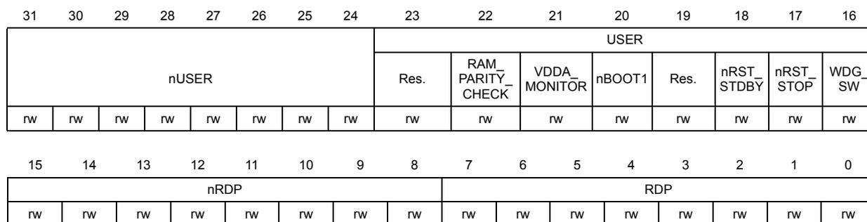
| 31 | 30 | 29 | 28 | 27 | 26 | 25 | 24 | 23 | 22 | 21 | 20 | 19 | 18 | 17 | 16 |
|---|---|---|---|---|---|---|---|---|---|---|---|---|---|---|---|
| nUSER | USER | ||||||||||||||
| Res. | RAM_ PARITY_ CHECK | VDDA_ MONITOR | nBOOT1 | Res. | nRST_ STDBY | nRST_ STOP | WDG_ SW | ||||||||
| rw | rw | rw | rw | rw | rw | rw | rw | rw | rw | rw | rw | rw | rw | rw | rw |
| 15 | 14 | 13 | 12 | 11 | 10 | 9 | 8 | 7 | 6 | 5 | 4 | 3 | 2 | 1 | 0 |
|---|---|---|---|---|---|---|---|---|---|---|---|---|---|---|---|
| nRDP | RDP | ||||||||||||||
| rw | rw | rw | rw | rw | rw | rw | rw | rw | rw | rw | rw | rw | rw | rw | rw |
Bits 31:24 nUSER : User option byte complement
Bit 23 Reserved, must be kept as “1”
Bits 22:20 USER : User option byte (stored in FLASH_OBR[15:8])
Bit 22: RAM_PARITY_CHECK
0: RAM parity check enabled
1: RAM parity check disabled
Bit 21: VDDA_MONITOR
0: V DDA power supply supervisor disabled
1: V DDA power supply supervisor enabled
Bit 20: nBOOT1
Together with the BOOT0 signal, it selects the device boot mode. Refer to Section 2.5: Boot configuration for more details.
Section 2.5: Boot configuration
Bit 19 Reserved, must be kept as “1”
Bits 18:16 Bit 18: nRST_STDBY
0: Reset generated when entering Standby mode.
1: No reset generated.
Bit 17: nRST_STOP
0: Reset generated when entering Stop mode
1: No reset generated
Bit 16: WDG_SW
0: Hardware watchdog
1: Software watchdog
Bits 15:8 nRDP : Read protection option byte complement
Bits 7:0 RDP : Read protection option byte
The value of this byte defines the flash memory protection level
0xAA: level 0 (ST production configuration)
0xXX (except 0xAA & 0xCC): Level 1
0xCC: Level 2
Note: Read protection level status is stored in bits RDPRT[1:0] of the Flash Option byte register (FLASH_OBR) . For more details about read protection, refer to Section 3.3.1: Read protection .
4.1.2 User data option byte
Flash memory address: 0x1FFF F804
ST production value: 0x00FF 00FF
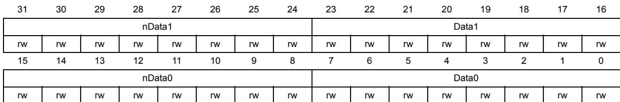
| 31 | 30 | 29 | 28 | 27 | 26 | 25 | 24 | 23 | 22 | 21 | 20 | 19 | 18 | 17 | 16 |
| nData1 | Data1 | ||||||||||||||
| rw | rw | rw | rw | rw | rw | rw | rw | rw | rw | rw | rw | rw | rw | rw | rw |
| 15 | 14 | 13 | 12 | 11 | 10 | 9 | 8 | 7 | 6 | 5 | 4 | 3 | 2 | 1 | 0 |
| nData0 | Data0 | ||||||||||||||
| rw | rw | rw | rw | rw | rw | rw | rw | rw | rw | rw | rw | rw | rw | rw | rw |
Bits 31:24 nData1 : User data byte 1 complement
Bits 23:16 Data1 : User data byte 1 value (stored in FLASH_OBR[31:24])
Bits 15:8 nData0 : User data byte 0 complement
Bits 7:0 Data0 : User data byte 0 value (stored in FLASH_OBR[23:16])
4.1.3 Write protection option byte
This set of registers is used to write-protect the flash memory. Clearing a bit in WRPx field (and at the same time setting a corresponding bit in nWRPx field) write-protects the given memory sector.
For STM32F030x4, STM32F030x6, STM32F070x6, STM32F030x8 and STM32F070xB devices, WRP bits from 0 to 31 are protecting the flash memory by sector of 4 kB.
For STM32F030xC devices, WRP bits from 0 to 30 are protecting the first 124 kB by sector of 4 kB and the bit 31 is protecting the last 132 kB.
Refer to Section 3.3.2: Write protection for more details.
Flash memory address: 0x1FFF F808
ST production value: 0x00FF 00FF
| 31 | 30 | 29 | 28 | 27 | 26 | 25 | 24 | 23 | 22 | 21 | 20 | 19 | 18 | 17 | 16 |
|---|---|---|---|---|---|---|---|---|---|---|---|---|---|---|---|
| nWRP1 | WRP1 | ||||||||||||||
| rw | rw | rw | rw | rw | rw | rw | rw | rw | rw | rw | rw | rw | rw | rw | rw |
| 15 | 14 | 13 | 12 | 11 | 10 | 9 | 8 | 7 | 6 | 5 | 4 | 3 | 2 | 1 | 0 |
| nWRP0 | WRP0 | ||||||||||||||
| rw | rw | rw | rw | rw | rw | rw | rw | rw | rw | rw | rw | rw | rw | rw | rw |
Bits 31:24 nWRP1 : Flash memory write protection option byte 1 complement
Bits 23:16 WRP1 : Flash memory write protection option byte 1 value (stored in FLASH_WRPR[15:8])
Bits 15:8 nWRP0 : Flash memory write protection option byte 0 complement
Bits 7:0 WRP0 : Flash memory write protection option byte 0 value (stored in FLASH_WRPR[7:0])
Note: STM32F030x4, STM32F030x6 and STM32F070x6 devices embed WRP0 and nWRP0 only.
The following Option byte are available on STM32F070xB and STM32F030xC devices only.
Flash memory address: 0x1FFF F80C
ST production value: 0x00FF 00FF
4.1.4 Option byte map
The following table summarizes the option bytes.
Table 12. Option byte map and ST production values
| Offset | Option byte | 31 | 30 | 29 | 28 | 27 | 26 | 25 | 24 | 23 | 22 | 21 | 20 | 19 | 18 | 17 | 16 | 15 | 14 | 13 | 12 | 11 | 10 | 9 | 8 | 7 | 6 | 5 | 4 | 3 | 2 | 1 | 0 |
|---|---|---|---|---|---|---|---|---|---|---|---|---|---|---|---|---|---|---|---|---|---|---|---|---|---|---|---|---|---|---|---|---|---|
| 0x00 | User and read protection | nUSER | USER | nRDP | RDP | ||||||||||||||||||||||||||||
| ST production value | Res. | RAM_PARITY_CHECK | VDDA_MONITOR | nBOOT1 | Res. | nRST_STDBY | nRST_STOP | WDG_SW | |||||||||||||||||||||||||
| 0x04 | User data | nData1 | Data1 | nData0 | Data0 | ||||||||||||||||||||||||||||
| 0x08 | Write protection | nWRP1 | WRP1 | nWRP0 | WRP0 | ||||||||||||||||||||||||||||
| ST production value | 0 | 0 | 0 | 0 | 0 | 0 | 0 | 0 | 1 | 1 | 1 | 1 | 1 | 1 | 1 | 1 | 0 | 0 | 0 | 0 | 0 | 0 | 0 | 0 | 0 | 0 | 1 | 1 | 1 | 1 | 1 | 1 | |
| 0x0C | Write protection | nWRP3 | WRP3 | nWRP2 | WRP2 | ||||||||||||||||||||||||||||
| ST production value | 0 | 0 | 0 | 0 | 0 | 0 | 0 | 0 | 1 | 1 | 1 | 1 | 1 | 1 | 1 | 1 | 0 | 0 | 0 | 0 | 0 | 0 | 0 | 0 | 0 | 0 | 1 | 1 | 1 | 1 | 1 | 1 | |