2. System and memory overview
2.1 System architecture
The main system consists of:
- • Two masters:
- – Arm ® Cortex ® -M0 core
- – General-purpose DMA
- • Four slaves:
- – Internal SRAM
- – Internal flash memory
- – AHB1 with AHB to APB bridge, which connects all the APB peripherals
- – AHB2 dedicated to GPIO ports
These are interconnected using a multilayer AHB bus architecture, as shown in Figure 1 :
Figure 1. System architecture
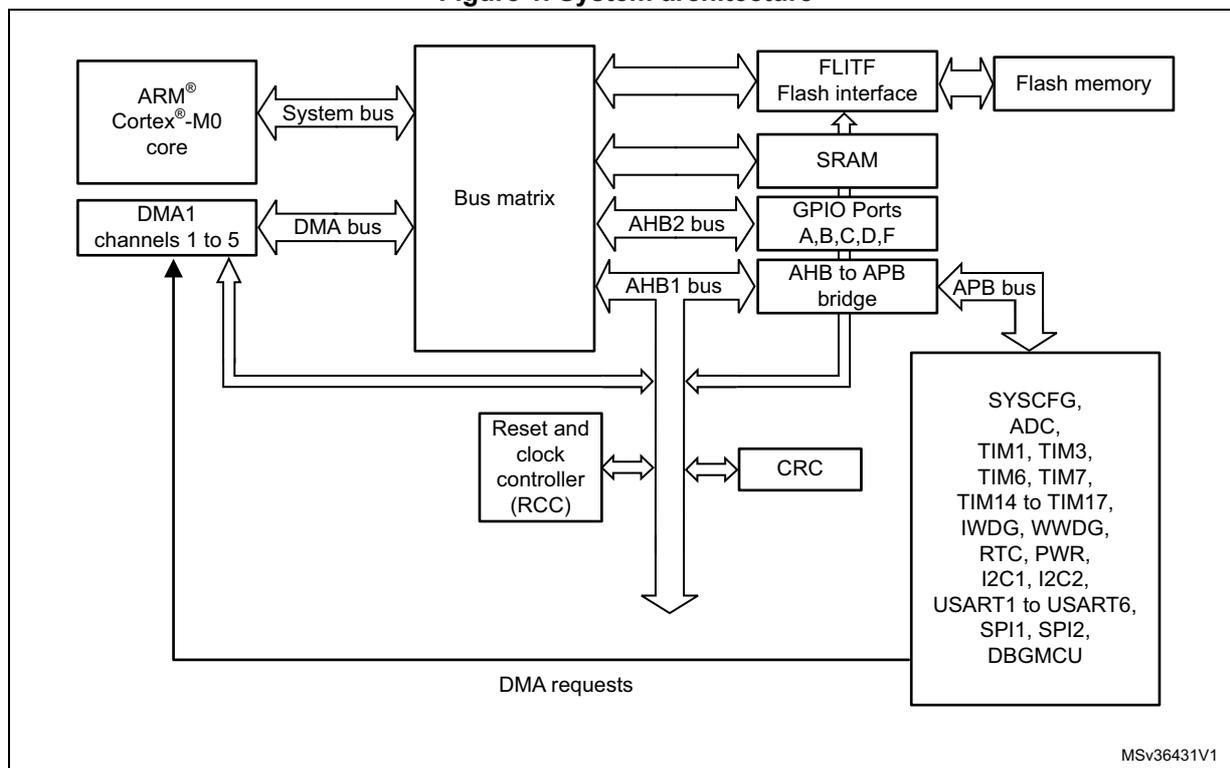
The diagram illustrates the system architecture. At the top left, the ARM ® Cortex ® -M0 core and DMA1 channels 1 to 5 are connected to a central Bus matrix via a System bus and a DMA bus, respectively. The Bus matrix is connected to several components: FLITF Flash interface (which connects to Flash memory), SRAM, GPIO Ports A,B,C,D,F (connected via the AHB2 bus), and an AHB to APB bridge (connected via the AHB1 bus). The AHB to APB bridge connects to a large block of APB peripherals, which includes SYSCFG, ADC, TIM1, TIM3, TIM6, TIM7, TIM14 to TIM17, IWDG, WWDG, RTC, PWR, I2C1, I2C2, USART1 to USART6, SPI1, SPI2, and DBGMCU. Below the Bus matrix, the Reset and clock controller (RCC) and CRC are connected to the AHB1 bus. DMA requests are shown as arrows from the APB peripherals block back to the DMA1 channels. The diagram is labeled MSV36431V1 in the bottom right corner.
System bus
This bus connects the system bus of the Arm ® Cortex ® -M0 core (peripherals bus) to a BusMatrix which manages the arbitration between the core and the DMA.
DMA bus
This bus connects the AHB master interface of the DMA to the BusMatrix which manages the access of CPU and DMA to SRAM, flash memory and peripherals.
BusMatrix
The BusMatrix manages the access arbitration between the core system bus and the DMA master bus. The arbitration uses a Round Robin algorithm. The BusMatrix is composed of two masters (CPU, DMA) and four slaves (FLITF, SRAM, AHB1 with AHB to APB bridge and AHB2).
AHB peripherals are connected on system bus through a BusMatrix to allow DMA access.
AHB to APB bridge (APB)
The AHB to APB bridge provides full synchronous connections between the AHB and the APB bus.
Refer to Section 2.2.2: Memory map and register boundary addresses for the address mapping of the peripherals connected to this bridge.
After each device reset, all peripheral clocks are disabled (except for the SRAM and flash). Before using a peripheral you have to enable its clock in the RCC_AHBENR, RCC_APB2ENR or RCC_APB1ENR register.
Note: When a 16- or 8-bit access is performed on an APB register, the access is transformed into a 32-bit access: the bridge duplicates the 16- or 8-bit data to feed the 32-bit vector.
2.2 Memory organization
2.2.1 Introduction
Program memory, data memory, registers and I/O ports are organized within the same linear 4-Gbyte address space.
The bytes are coded in memory in Little Endian format. The lowest numbered byte in a word is considered the word's least significant byte and the highest numbered byte the most significant.
The addressable memory space is divided into eight main blocks, of 512 Mbytes each.
2.2.2 Memory map and register boundary addresses
Figure 2. Memory map
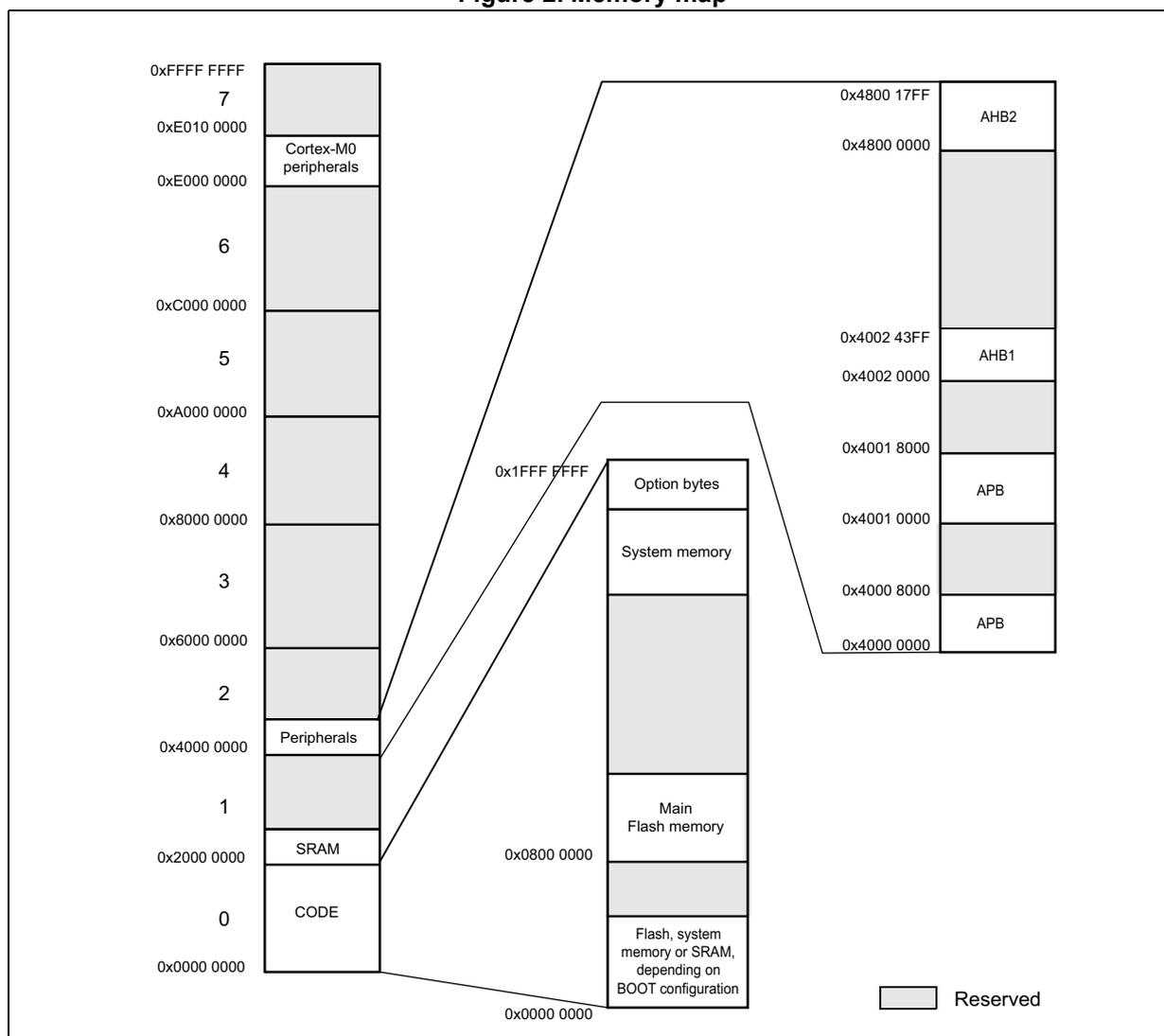
Memory map details:
- Main Memory Map (Left Column):
- 0x0000 0000 to 0x2000 0000: CODE
- 0x2000 0000 to 0x4000 0000: SRAM
- 0x4000 0000 to 0x6000 0000: Reserved
- 0x6000 0000 to 0x8000 0000: Reserved
- 0x8000 0000 to 0xA000 0000: Reserved
- 0xA000 0000 to 0xC000 0000: Reserved
- 0xC000 0000 to 0xE000 0000: Reserved
- 0xE000 0000 to 0xFFFF FFFF: Cortex-M0 peripherals
- Peripheral Memory Map (Right Column):
- 0x4000 0000 to 0x4001 8000: APB
- 0x4001 8000 to 0x4002 0000: Reserved
- 0x4002 0000 to 0x4002 43FF: AHB1
- 0x4002 43FF to 0x4800 0000: Reserved
- 0x4800 0000 to 0x4800 17FF: AHB2
- Internal Structure of Segment 0 (Callout):
- 0x0000 0000 to 0x0800 0000: Flash, system memory or SRAM, depending on BOOT configuration
- 0x0800 0000 to 0x1000 0000: Main Flash memory
- 0x1000 0000 to 0x1800 0000: System memory
- 0x1800 0000 to 0x1FFF FFFF: Option bytes
Legend: Reserved
All the memory map areas not allocated to on-chip memories and peripherals are considered “Reserved”. For the detailed mapping of available memory and register areas, refer to the following table, which gives the boundary addresses of the available peripherals.
Table 1. STM32F0x0 memory boundary addresses
| Device | Boundary address | Size | Memory Area | Register description |
|---|---|---|---|---|
| STM32F030x4, STM32F030x6 | 0x2000 1000 - 0x3FFF FFFF | ~512 MB | Reserved | - |
| 0x2000 0000 - 0x2000 0FFF | 4 KB | SRAM | Section 2.3 on page 42 | |
| 0x1FFF FC00 - 0x1FFF FFFF | 1 KB | Reserved | - | |
| 0x1FFF F800 - 0x1FFF FBFF | 1 KB | Option bytes | Section 4 on page 66 | |
| 0x1FFF EC00 - 0x1FFF F7FF | 3 KB | System memory | - | |
| 0x0800 8000 - 0x1FFF EBFF | ~384 MB | Reserved | - | |
| 0x0800 0000 - 0x0800 7FFF | 32 KB (1) | Main flash memory | Section 3 on page 46 | |
| 0x0000 8000 - 0x07FF FFFF | ~128 MB | Reserved | - | |
| 0x0000 0000 - 0x0000 7FFF | 32 KB (1) | Main flash memory, system memory or SRAM depending on BOOT configuration | - | |
| STM32F070x6 | 0x2000 1800 - 0x3FFF FFFF | ~512 MB | Reserved | - |
| 0x2000 0000 - 0x2000 17FF | 6 KB | SRAM | Section 2.3 on page 42 | |
| 0x1FFF FC00 - 0x1FFF FFFF | 1 KB | Reserved | - | |
| 0x1FFF F800 - 0x1FFF FBFF | 1 KB | Option bytes | Section 4 on page 66 | |
| 0x1FFF C400 - 0x1FFF F7FF | 13 KB | System memory | - | |
| 0x0801 8000 - 0x1FFF C7FF | ~384 MB | Reserved | - | |
| 0x0800 0000 - 0x0801 7FFF | 32 KB | Main flash memory | Section 3 on page 46 | |
| 0x0001 8000 - 0x07FF FFFF | ~128 MB | Reserved | - | |
| 0x0000 0000 - 0x0000 7FFF | 32 KB | Main flash memory, system memory or SRAM depending on BOOT configuration | - | |
| STM32F030x8 | 0x2000 2000 - 0x3FFF FFFF | ~512 MB | Reserved | - |
| 0x2000 0000 - 0x2000 1FFF | 8 KB | SRAM | Section 2.3 on page 42 | |
| 0x1FFF FC00 - 0x1FFF FFFF | 1 KB | Reserved | - | |
| 0x1FFF F800 - 0x1FFF FBFF | 1 KB | Option bytes | Section 4 on page 66 | |
| 0x1FFF EC00 - 0x1FFF F7FF | 3 KB | System memory | - | |
| 0x0801 0000 - 0x1FFF EBFF | ~384 MB | Reserved | - | |
| 0x0800 0000 - 0x0800 FFFF | 64 KB | Main flash memory | Section 3 on page 46 | |
| 0x0001 0000 - 0x07FF FFFF | ~128 MB | Reserved | - | |
| 0x0000 0000 - 0x0000 FFFF | 64 KB | Main flash memory, system memory or SRAM depending on BOOT configuration | - |
| Device | Boundary address | Size | Memory Area | Register description |
|---|---|---|---|---|
| STM32F070xB | 0x2000 4000 - 0x3FFF FFFF | ~512 MB | Reserved | - |
| 0x2000 0000 - 0x2000 3FFF | 16 KB | SRAM | Section 2.3 on page 42 | |
| 0x1FFF F800 - 0x1FFF FFFF | 2 KB | Option bytes | Section 4 on page 66 | |
| 0x1FFF C800 - 0x1FFF F7FF | 12 KB | System memory | - | |
| 0x0802 0000 - 0x1FFF C7FF | ~384 MB | Reserved | - | |
| 0x0800 0000 - 0x0801 FFFF | 128 KB | Main flash memory | Section 3 on page 46 | |
| 0x0002 0000 - 0x07FF FFFF | ~128 MB | Reserved | - | |
| 0x0000 0000 - 0x0001 FFFF | 128 KB | Main flash memory, system memory or SRAM depending on BOOT configuration | - | |
| STM32F030xC | 0x2000 8000 - 0x3FFF FFFF | ~512 MB | Reserved | - |
| 0x2000 0000 - 0x2000 7FFF | 32 KB | SRAM | Section 2.3 on page 42 | |
| 0x1FFF F800 - 0x1FFF FFFF | 2 KB | Option bytes | Section 4 on page 66 | |
| 0x1FFF D800 - 0x1FFF F7FF | 8 KB | System memory | - | |
| 0x0804 0000 - 0x1FFF D7FF | ~384 MB | Reserved | - | |
| 0x0800 0000 - 0x0803 FFFF | 256 KB | Main flash memory | Section 3 on page 46 | |
| 0x0004 0000 - 0x07FF FFFF | ~128 MB | Reserved | - | |
| 0x0000 0000 - 0x0003 FFFF | 256 KB | Main flash memory, system memory or SRAM depending on BOOT configuration | - |
1. Limited to 16 KB on STM32F030x4 devices.
Table 2. STM32F0x0 peripheral register boundary addresses| Bus | Boundary address | Size | Peripheral | Peripheral register map |
|---|---|---|---|---|
| - | 0xE000 0000 - 0xE00F FFFF | 1MB | Cortex ® -M0 internal peripherals | - |
| - | 0x4800 1800 - 0x5FFF FFFF | ~384 MB | Reserved | - |
| AHB2 | 0x4800 1400 - 0x4800 17FF | 1KB | GPIOF | Section 8.4.11 on page 139 |
| 0x4800 1000 - 0x4800 13FF | 1KB | Reserved | - | |
| 0x4800 0C00 - 0x4800 0FFF | 1KB | GPIOE | Section 8.4.11 on page 139 | |
| 0x4800 0800 - 0x4800 0BFF | 1KB | GPIOC | Section 8.4.11 on page 139 | |
| 0x4800 0400 - 0x4800 07FF | 1KB | GPIOB | Section 8.4.11 on page 139 | |
| 0x4800 0000 - 0x4800 03FF | 1KB | GPIOA | Section 8.4.11 on page 139 | |
| - | 0x4002 4400 - 0x47FF FFFF | ~128 MB | Reserved | - |
Table 2. STM32F0x0 peripheral register boundary addresses (continued)
| Bus | Boundary address | Size | Peripheral | Peripheral register map |
|---|---|---|---|---|
| AHB1 | 0x4002 3400 - 0x4002 43FF | 4 KB | Reserved | - |
| 0x4002 3000 - 0x4002 33FF | 1 KB | CRC | Section 5.4.5 on page 75 | |
| 0x4002 2400 - 0x4002 2FFF | 3 KB | Reserved | - | |
| 0x4002 2000 - 0x4002 23FF | 1 KB | FLASH interface | Section 3.5.9 on page 65 | |
| 0x4002 1400 - 0x4002 1FFF | 3 KB | Reserved | - | |
| 0x4002 1000 - 0x4002 13FF | 1 KB | RCC | Section 7.4.15 on page 123 | |
| 0x4002 0400 - 0x4002 0FFF | 3 KB | Reserved | - | |
| 0x4002 0000 - 0x4002 03FF | 1 KB | DMA | Section 10.6.8 on page 169 | |
| - | 0x4001 8000 - 0x4001 FFFF | 32 KB | Reserved | - |
| APB | 0x4001 5C00 - 0x4001 7FFF | 9 KB | Reserved | - |
| 0x4001 5800 - 0x4001 5BFF | 1 KB | DBGMCU | - | |
| 0x4001 4C00 - 0x4001 57FF | 3 KB | Reserved | - | |
| 0x4001 4800 - 0x4001 4BFF | 1 KB | TIM17 | Section 17.6.17 on page 466 | |
| 0x4001 4400 - 0x4001 47FF | 1 KB | TIM16 | Section 17.6.17 on page 466 | |
| 0x4001 4000 - 0x4001 43FF | 1 KB | TIM15 | Section 17.5.19 on page 449 | |
| 0x4001 3C00 - 0x4001 3FFF | 1 KB | Reserved | - | |
| 0x4001 3800 - 0x4001 3BFF | 1 KB | USART1 | Section 23.7.11 on page 635 | |
| 0x4001 3400 - 0x4001 37FF | 1 KB | Reserved | - | |
| 0x4001 3000 - 0x4001 33FF | 1 KB | SPI1 | Section 24.6.8 on page 671 | |
| 0x4001 2C00 - 0x4001 2FFF | 1 KB | TIM1 | Section 13.4.21 on page 299 | |
| 0x4001 2800 - 0x4001 2BFF | 1 KB | Reserved | - | |
| 0x4001 2400 - 0x4001 27FF | 1 KB | ADC | Section 12.11 on page 223 | |
| 0x4001 1800 - 0x4001 23FF | 4 KB | Reserved | - | |
| 0x4001 1400 - 0x4001 17FF | 1 KB | USART6 | Section 23.7.11 on page 635 | |
| 0x4001 0800 - 0x4001 23FF | 7 KB | Reserved | - | |
| 0x4001 0400 - 0x4001 07FF | 1 KB | EXTI | Section 11.3.7 on page 181 | |
| 0x4001 0000 - 0x4001 03FF | 1 KB | SYSCFG | Section 9.1.7 on page 148 | |
| - | 0x4000 8000 - 0x4000 FFFF | 32 KB | Reserved | - |
| Bus | Boundary address | Size | Peripheral | Peripheral register map |
|---|---|---|---|---|
| APB | 0x4000 7400 - 0x4000 7FFF | 3 KB | Reserved | - |
| 0x4000 7000 - 0x4000 73FF | 1 KB | PWR | Section 6.4.3 on page 87 | |
| 0x4000 63FF - 0x4000 6FFF | 3 KB | Reserved | - | |
| 0x4000 6000 - 0x4000 63FF | 1 KB | USB/SRAM | Section 25.6.3 on page 703 | |
| 0x4000 5C00 - 0x4000 5FFF | 1 KB | USB | Section 25.6.3 on page 703 | |
| 0x4000 5800 - 0x4000 5BFF | 1 KB | I2C2 | Section 22.7.12 on page 588 | |
| 0x4000 5400 - 0x4000 57FF | 1 KB | I2C1 | Section 22.7.12 on page 588 | |
| 0x4000 5000 - 0x4000 53FF | 1 KB | USART5 | Section 23.7.11 on page 635 | |
| 0x4000 4C00 - 0x4000 4FFF | 1 KB | USART4 | Section 23.7.11 on page 635 | |
| 0x4000 4800 - 0x4000 4BFF | 1 KB | USART3 | Section 23.7.11 on page 635 | |
| 0x4000 4400 - 0x4000 47FF | 1 KB | USART2 | Section 23.7.11 on page 635 | |
| 0x4000 3C00 - 0x4000 43FF | 2 KB | Reserved | - | |
| 0x4000 3800 - 0x4000 3BFF | 1 KB | SPI2 | Section 24.6.8 on page 671 | |
| 0x4000 3400 - 0x4000 37FF | 1 KB | Reserved | - | |
| 0x4000 3000 - 0x4000 33FF | 1 KB | IWDG | Section 19.4.6 on page 477 | |
| 0x4000 2C00 - 0x4000 2FFF | 1 KB | WWDG | Section 20.5.4 on page 483 | |
| 0x4000 2800 - 0x4000 2BFF | 1 KB | RTC | Section 21.7.17 on page 521 | |
| 0x4000 2400 - 0x4000 27FF | 1 KB | Reserved | - | |
| 0x4000 2000 - 0x4000 23FF | 1 KB | TIM14 | Section 16.4.13 on page 399 | |
| 0x4000 1800 - 0x4000 1FFF | 2 KB | Reserved | - | |
| 0x4000 1400 - 0x4000 17FF | 1 KB | TIM7 | Section 15.4.8 on page 379 | |
| 0x4000 1000 - 0x4000 13FF | 1 KB | TIM6 | Section 15.4.8 on page 379 | |
| 0x4000 0800 - 0x4000 0FFF | 2 KB | Reserved | - | |
| 0x4000 0400 - 0x4000 07FF | 1 KB | TIM3 | Section 14.4.19 on page 365 | |
| 0x4000 0000 - 0x4000 03FF | 1 KB | Reserved | - |
2.3 Embedded SRAM
STM32F030x4 and STM32F030x6 devices feature 4 Kbytes of SRAM. STM32F030x8 devices feature 8 Kbytes of SRAM. STM32F030xC devices feature 32 Kbytes of SRAM. STM32F070x6 devices feature 6 Kbytes of SRAM. STM32F070xB devices feature 16 Kbytes of SRAM.
The SRAM can be accessed by bytes, half-words (16 bits) or full words (32 bits), at maximum system clock frequency without wait state and thus by both CPU and DMA.
Parity check
The user can enable the parity check using the option bit RAM_PARITY_CHECK in the user option byte (refer to Section 4: Option bytes ).
The data bus width is 36 bits because 4 bits are available for parity check (1 bit per byte) in order to increase memory robustness, as required for instance by Class B or SIL norms.
The parity bits are computed and stored when writing into the SRAM. Then, they are automatically checked when reading. If one bit fails, an NMI is generated. In addition, to get the SRAM parity error at the same cycle time that it is occurring, a bus error is generated (triggering a HardFault exception) together with the NMI. This avoids the use of corrupted data by the application, but with the side effect of having both NMI and HardFault interrupts generated. The same error can also be linked to the BRK_IN Break input of TIM1/15/16/17, with the SRAM_PARITY_LOCK control bit in the SYSCFG configuration register 2 (SYSCFG_CFGR2) . The SRAM Parity Error flag (SRAM_PEF) is available in the SYSCFG configuration register 2 (SYSCFG_CFGR2) .
Note: When enabling the RAM parity check, it is advised to initialize by software the whole RAM memory at the beginning of the code, to avoid getting parity errors when reading non-initialized locations.
2.4 Flash memory overview
The flash memory is composed of two distinct physical areas:
- • The main flash memory block. It contains the application program and user data if necessary.
- • The information block. It is composed of two parts:
- – option bytes for hardware and memory protection user configuration
- – system memory which contains the proprietary boot loader code (refer to Section 3: Embedded flash memory for more details.)
The flash interface implements instruction access and data access based on the AHB protocol. It implements the prefetch buffer that speeds up CPU code execution. It also implements the logic necessary to carry out the flash memory operations (Program/Erase) controlled through the flash registers.
2.5 Boot configuration
In the STM32F0x0, three different boot modes can be selected through the BOOT0 pin and boot configuration bits nBOOT1 in the User option byte, as shown in the following table.
Table 3. Boot modes
| Boot mode configuration | Mode | |
|---|---|---|
| nBOOT1 bit | BOOT0 pin | |
| x | 0 | Main Flash memory is selected as boot area (1) |
| 1 | 1 | System memory is selected as boot area |
| 0 | 1 | Embedded SRAM is selected as boot area |
1. For STM32F070x6 and STM32F030xC devices, see also Empty check description.
The boot mode configuration is latched on the 4th rising edge of SYSCLK after a reset. It is up to the user to set boot mode configuration related to the required boot mode.
The boot mode configuration is also re-sampled when exiting from Standby mode. Consequently they must be kept in the required Boot mode configuration in Standby mode. After this startup delay has elapsed, the CPU fetches the top-of-stack value from address 0x0000 0000, then starts code execution from the boot memory at 0x0000 0004.
Depending on the selected boot mode, main flash memory, system memory or SRAM is accessible as follows:
- • Boot from main flash memory: the main flash memory is aliased in the boot memory space (0x0000 0000), but still accessible from its original memory space (0x0800 0000). In other words, the flash memory contents can be accessed starting from address 0x0000 0000 or 0x0800 0000.
- • Boot from system memory: the system memory is aliased in the boot memory space (0x0000 0000), but still accessible from its original memory space (0x1FFF EC00 on STM32F030x4, STM32F030x6 and STM32F030x8 devices, 0x1FFF C400 on STM32F070x6 devices, 0x1FFF C800 on STM32F070xB and 0x1FFF D800 on STM32F030xC devices).
- • Boot from the embedded SRAM: the SRAM is aliased in the boot memory space (0x0000 0000), but it is still accessible from its original memory space (0x2000 0000).
Empty check
On STM32F070x6 and STM32F030xC devices only, internal empty check flag is implemented to allow easy programming of virgin devices by the boot loader. This flag is used when BOOT0 pin is defining Main flash memory as the target boot area. When the flag is set, the device is considered as empty and System memory (boot loader) is selected instead of the main flash as a boot area to allow user to program the flash memory.
Therefore, some of the GPIOs are reconfigured from the High-Z state. Refer to AN2606 for more details concerning the boot loader and GPIO configuration in System memory boot mode. It is possible to disable this feature by configuring the option bytes, to force boot from the Main flash memory (nSWBOOT0 = 0, nBOOT0 = 1).
The empty check flag is updated only during the loading of option bytes: it is set when the content of the address 0x0800 0000 is read as 0xFFFF FFFF, otherwise it is cleared. It
means a power reset or setting of OBL_LAUNCH bit in FLASH_CR register is needed to clear this flag after programming of a virgin device to execute user code after System reset.
Note: If the device is programmed for a first time but the option bytes are not reloaded, the device still selects System memory as a boot area after a System reset. In the STM32F070x6, the boot loader code is able to detect this situation. It then changes the boot memory mapping to main flash and performs a jump to user code programmed there. In the STM32F030xC, a POR must be performed or the Option bytes reloaded before applying the system reset.
Physical remap
Once the boot mode is selected, the application software can modify the memory accessible in the code area. This modification is performed by programming the MEM_MODE bits in the SYSCFG configuration register 1 (SYSCFG_CFGR1) . Unlike Cortex ® M3 and M4, the M0 CPU does not support the vector table relocation. For application code which is located in a different address than 0x0800 0000, some additional code must be added in order to be able to serve the application interrupts. A solution is to relocate by software the vector table to the internal SRAM:
- • Copy the vector table from the flash (mapped at the base of the application load address) to the base address of the SRAM at 0x2000 0000.
- • Remap SRAM at address 0x0000 0000, using SYSCFG configuration register 1.
- • Then once an interrupt occurs, the Cortex ® -M0 processor fetches the interrupt handler start address from the relocated vector table in SRAM, then it jumps to execute the interrupt handler located in the flash.
This operation should be done at the initialization phase of the application. Please refer to AN4065 and attached IAP code from www.st.com for more details.
Embedded boot loader
The embedded boot loader is located in the System memory, programmed by ST during production. It is used to reprogram the flash memory using one of the following serial interfaces:
- • USART on pins PA14/PA15 or PA9/PA10
- • I2C on pins PB6/PB7 (STM32F070xx and STM32F030xC devices only)
- • USB DFU interface (STM32F070xx devices only)
For further details, refer to the application note AN2606.