28. AES hardware accelerator (AES)
This section applies to STM32L486/L4A6 devices only.
28.1 Introduction
The AES hardware accelerator (AES) encrypts or decrypts data, using an algorithm and implementation fully compliant with the advanced encryption standard (AES) defined in Federal information processing standards (FIPS) publication 197.
Multiple chaining modes are supported (ECB, CBC, CTR, GCM, GMAC, CCM), for key sizes of 128 or 256 bits.
The AES accelerator is a 32-bit AHB peripheral. It supports DMA single transfers for incoming and outgoing data (two DMA channels required).
The AES peripheral provides hardware acceleration to AES cryptographic algorithms packaged in STM32 cryptographic library.
AES is an AMBA AHB slave peripheral, accessible through 32-bit word single accesses only (otherwise an AHB bus error is generated and write accesses are ignored).
28.2 AES main features
- • Compliance with NIST “ Advanced encryption standard (AES), FIPS publication 197 ” from November 2001
- • 128-bit data block processing
- • Support for cipher key lengths of 128-bit and 256-bit
- • Encryption and decryption with multiple chaining modes:
- – Electronic codebook (ECB) mode
- – Cipher block chaining (CBC) mode
- – Counter (CTR) mode
- – Galois counter mode (GCM)
- – Galois message authentication code (GMAC) mode
- – Counter with CBC-MAC (CCM) mode
- • 51 or 75 clock cycle latency in ECB mode for processing one 128-bit block of data with, respectively, 128-bit or 256-bit key
- • Integrated key scheduler with its key derivation stage (ECB or CBC decryption only)
- • AMBA AHB slave peripheral, accessible through 32-bit word single accesses only
- • 256-bit register for storing the cryptographic key (eight 32-bit registers)
- • 128-bit register for storing initialization vector (four 32-bit registers)
- • 32-bit buffer for data input and output
- • Automatic data flow control with support of single-transfer direct memory access (DMA) using two channels (one for incoming data, one for processed data)
- • Data-swapping logic to support 1-, 8-, 16- or 32-bit data
- • Possibility for software to suspend a message if AES needs to process another message with a higher priority, then resume the original message
28.3 AES implementation
The device has a single instance of AES peripheral.
28.4 AES functional description
28.4.1 AES block diagram
Figure 190 shows the block diagram of AES.
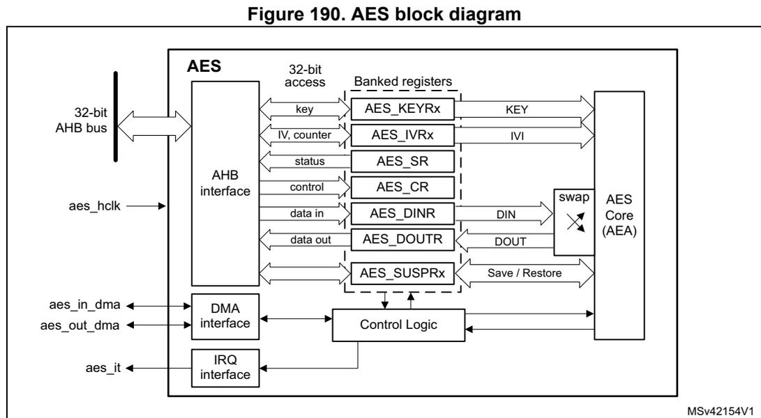
28.4.2 AES internal signals
Table 179 describes the user relevant internal signals interfacing the AES peripheral.
Table 179. AES internal input/output signals
| Signal name | Signal type | Description |
|---|---|---|
| aes_hclk | digital input | AHB bus clock |
| aes_it | digital output | AES interrupt request |
| aes_in_dma | digital input/output | Input DMA single request/acknowledge |
| aes_out_dma | digital input/output | Output DMA single request/acknowledge |
28.4.3 AES cryptographic core
Overview
The AES cryptographic core consists of the following components:
- • AES algorithm (AEA)
- • multiplier over a binary Galois field (GF2mul)
- • key input
- • initialization vector (IV) input
- • chaining algorithm logic (XOR, feedback/counter, mask)
The AES core works on 128-bit data blocks (four words) with 128-bit or 256-bit key length. Depending on the chaining mode, the AES requires zero or one 96-bit initialization vector IV (and a 32-bit counter field).
The AES features the following modes of operation:
- •
Mode 1:
Plaintext encryption using a key stored in the AES_KEYRx registers - •
Mode 2:
ECB or CBC decryption key preparation. It must be used prior to selecting Mode 3 with ECB or CBC chaining modes. The key prepared for decryption is stored automatically in the AES_KEYRx registers. Now the AES peripheral is ready to switch to Mode 3 for executing data decryption. - •
Mode 3:
Ciphertext decryption using a key stored in the AES_KEYRx registers. When ECB and CBC chaining modes are selected, the key must be prepared beforehand, through Mode 2. - •
Mode 4:
ECB or CBC ciphertext single decryption using the key stored in the AES_KEYRx registers (the initial key is derived automatically).
Note: Mode 2 and mode 4 are only used when performing ECB and CBC decryption. When Mode 4 is selected only one decryption can be done, therefore usage of Mode 2 and Mode 3 is recommended instead.
The operating mode is selected by programming the MODE[1:0] bitfield of the AES_CR register. It may be done only when the AES peripheral is disabled.
Typical data processing
Typical usage of the AES is described in Section 28.4.4: AES procedure to perform a cipher operation on page 828 .
Note: The outputs of the intermediate AEA stages are never revealed outside the cryptographic boundary, with the exclusion of the IVI bitfield.
Chaining modes
The following chaining modes are supported by AES, selected through the CHMOD[2:0] bitfield of the AES_CR register:
- • Electronic code book (ECB)
- • Cipher block chaining (CBC)
- • Counter (CTR)
- • Galois counter mode (GCM)
- • Galois message authentication code (GMAC)
- • Counter with CBC-MAC (CCM)
Note: The chaining mode may be changed only when AES is disabled (bit EN of the AES_CR register set).
Principle of each AES chaining mode is provided in the following subsections.
Detailed information is in dedicated sections, starting from Section 28.4.8: AES basic chaining modes (ECB, CBC) .
Electronic codebook (ECB) mode
Figure 191. ECB encryption and decryption principle
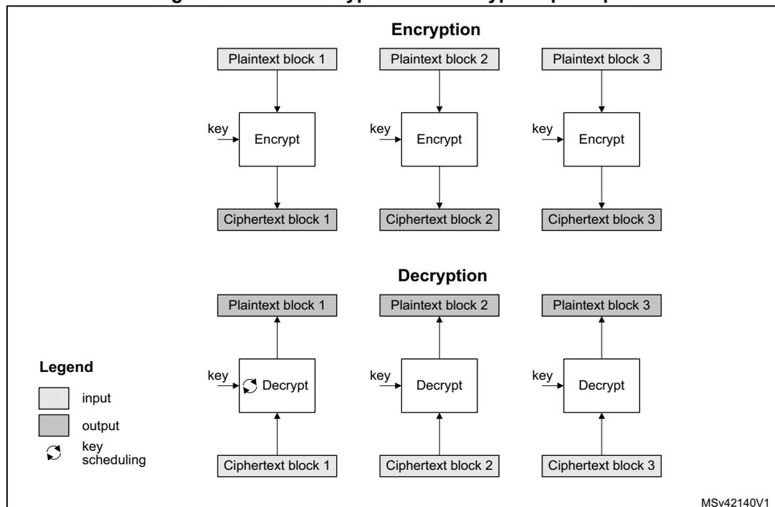
The diagram illustrates the ECB encryption and decryption process. It is divided into two horizontal sections: Encryption and Decryption .
Encryption: Three separate processing paths are shown. Each path starts with a Plaintext block (1, 2, or 3) entering an Encrypt block. A key is also input to each Encrypt block. The output of each Encrypt block is a Ciphertext block (1, 2, or 3).
Decryption: Three separate processing paths are shown. Each path starts with a Ciphertext block (1, 2, or 3) entering a Decrypt block. A key is also input to each Decrypt block. The output of each Decrypt block is a Plaintext block (1, 2, or 3). Notably, the first Decrypt block shows a circular arrow icon indicating key scheduling.
Legend:
- input (light gray box)
- output (dark gray box)
- key scheduling (circular arrow)
MSV42140V1
ECB is the simplest mode of operation. There are no chaining operations, and no special initialization stage. The message is divided into blocks and each block is encrypted or decrypted separately.
Note: For decryption, a special key scheduling is required before processing the first block.
Cipher block chaining (CBC) mode Figure 192. CBC encryption and decryption principle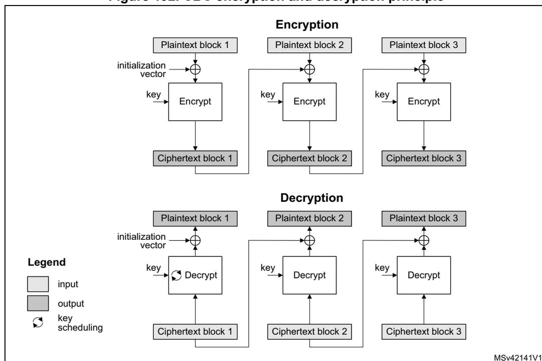
Encryption
Plaintext block 1, Plaintext block 2, Plaintext block 3
initialization vector
key
Encrypt
Ciphertext block 1, Ciphertext block 2, Ciphertext block 3
Decryption
Plaintext block 1, Plaintext block 2, Plaintext block 3
initialization vector
key
Decrypt
Ciphertext block 1, Ciphertext block 2, Ciphertext block 3
Legend
- input
- output
- key scheduling
MSv42141V1
In CBC mode the output of each block chains with the input of the following block. To make each message unique, an initialization vector is used during the first block processing.
Note: For decryption, a special key scheduling is required before processing the first block.
Counter (CTR) mode
Figure 193. CTR encryption and decryption principle
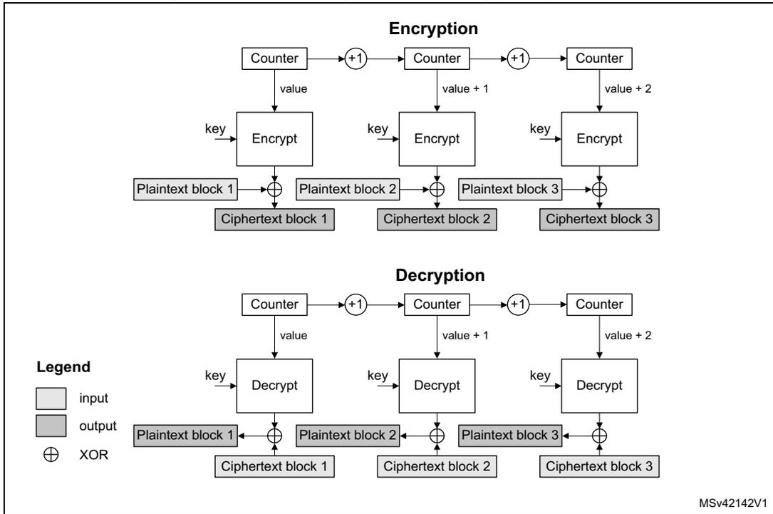
Encryption
Counter → (+1) → Counter → (+1) → Counter
value → Encrypt, key → Encrypt, Plaintext block 1 → XOR → Ciphertext block 1
value + 1 → Encrypt, key → Encrypt, Plaintext block 2 → XOR → Ciphertext block 2
value + 2 → Encrypt, key → Encrypt, Plaintext block 3 → XOR → Ciphertext block 3
Decryption
Counter → (+1) → Counter → (+1) → Counter
value → Decrypt, key → Decrypt, Ciphertext block 1 → XOR → Plaintext block 1
value + 1 → Decrypt, key → Decrypt, Ciphertext block 2 → XOR → Plaintext block 2
value + 2 → Decrypt, key → Decrypt, Ciphertext block 3 → XOR → Plaintext block 3
Legend
input (white rectangle)
output (gray rectangle)
XOR (circle with cross symbol)
MSv42142V1
The CTR mode uses the AES core to generate a key stream. The keys are then XORed with the plaintext to obtain the ciphertext as specified in NIST Special Publication 800-38A, Recommendation for Block Cipher Modes of Operation .
Note: Unlike with ECB and CBC modes, no key scheduling is required for the CTR decryption, since in this chaining scheme the AES core is always used in encryption mode for producing the key stream, or counter blocks.
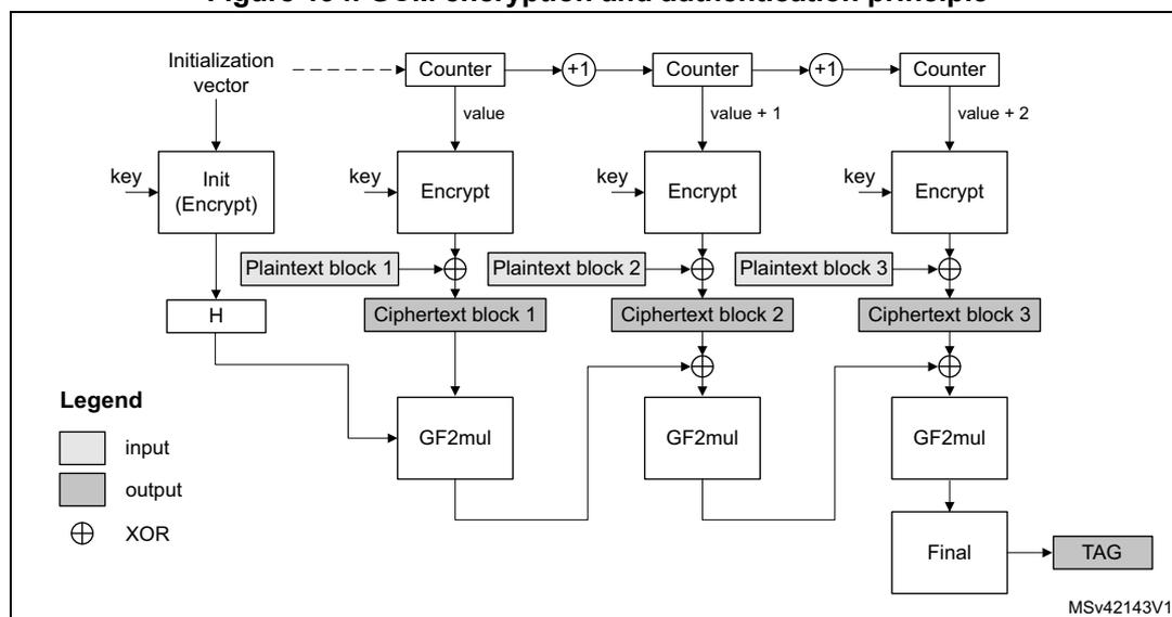
Galois/counter mode (GCM)
Figure 194. GCM encryption and authentication principle
Legend
- input
- output
- \( \oplus \) XOR
MSv42143V1
In Galois/counter mode (GCM), the plaintext message is encrypted while a message authentication code (MAC) is computed in parallel, thus generating the corresponding ciphertext and its MAC (also known as authentication tag). It is defined in NIST Special Publication 800-38D, Recommendation for Block Cipher Modes of Operation - Galois/Counter Mode (GCM) and GMAC .
GCM mode is based on AES in counter mode for confidentiality. It uses a multiplier over a fixed finite field for computing the message authentication code. It requires an initial value and a particular 128-bit block at the end of the message.
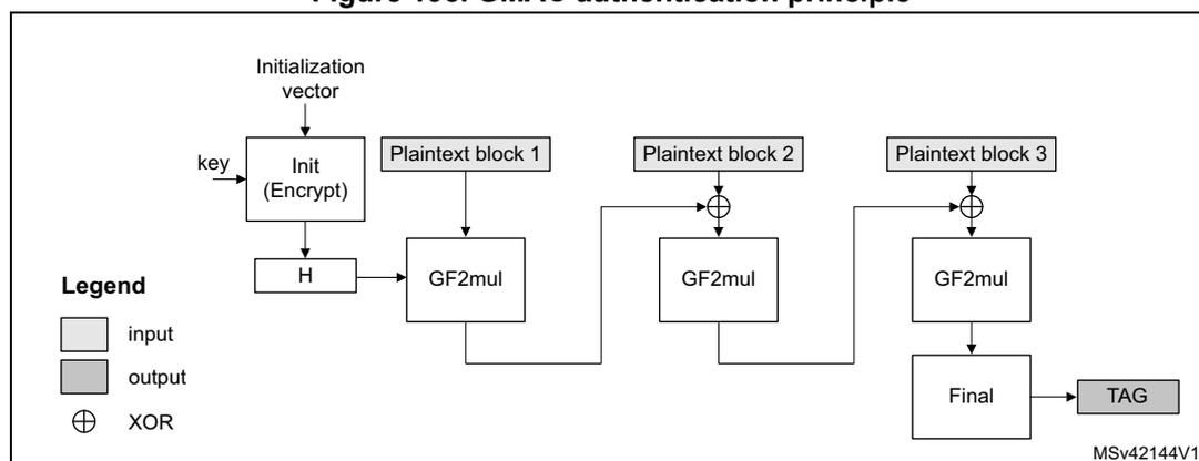
Galois message authentication code (GMAC) principle
Figure 195. GMAC authentication principle
Legend
- input
- output
- \( \oplus \) XOR
MSv42144V1
Galois message authentication code (GMAC) allows authenticating a message and generating the corresponding message authentication code (MAC). It is defined in NIST Special Publication 800-38D, Recommendation for Block Cipher Modes of Operation - Galois/Counter Mode (GCM) and GMAC .
GMAC is similar to GCM, except that it is applied on a message composed only by plaintext authenticated data (that is, only header, no payload).
Counter with CBC-MAC (CCM) principle
Figure 196. CCM encryption and authentication principle
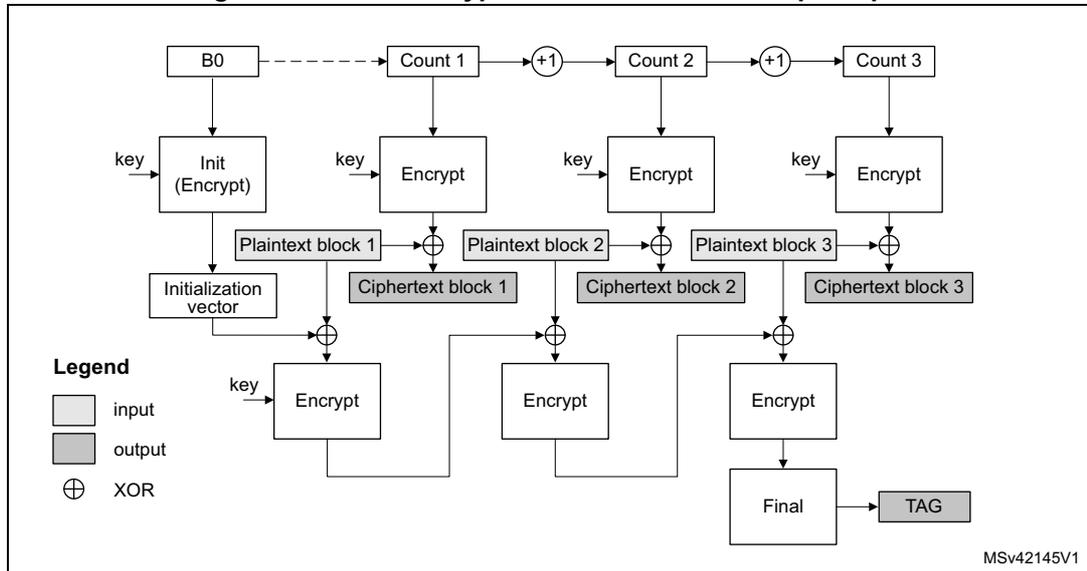
In Counter with cipher block chaining-message authentication code (CCM) mode, the plaintext message is encrypted while a message authentication code (MAC) is computed in parallel, thus generating the corresponding ciphertext and the corresponding MAC (also known as tag). It is described by NIST in Special Publication 800-38C, Recommendation for Block Cipher Modes of Operation - The CCM Mode for Authentication and Confidentiality .
CCM mode is based on AES in counter mode for confidentiality and it uses CBC for computing the message authentication code. It requires an initial value.
Like GCM, the CCM chaining mode can be applied on a message composed only by plaintext authenticated data (that is, only header, no payload). Note that this way of using CCM is not called CMAC (it is not similar to GCM/GMAC), and its usage is not recommended by NIST.
28.4.4 AES procedure to perform a cipher operation
Introduction
A typical cipher operation is explained below. Detailed information is provided in sections starting from Section 28.4.8: AES basic chaining modes (ECB, CBC) .
The flowcharts shown in Figure 197 and Figure 198 describe the way STM32 cryptographic library implements the AES algorithm. AES accelerates the execution of the AES-128 and AES-256 cryptographic algorithms in ECB, CBC, CTR, CCM, and GCM operating modes.
Note: For more details on the cryptographic library, refer to the UM1924 user manual “STM32 crypto library” available from www.st.com .
Figure 197. STM32 cryptolib AES flowchart examples
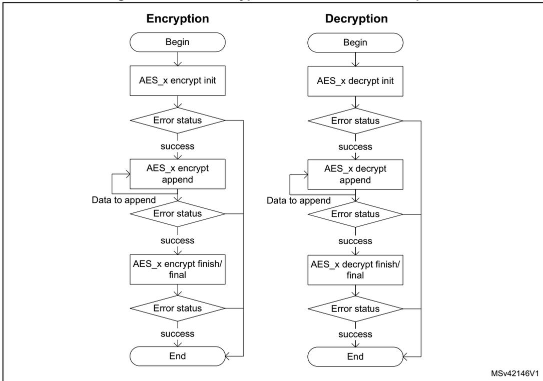
graph TD; subgraph Encryption; E1([Begin]) --> E2[AES_x encrypt init]; E2 --> E3{Error status}; E3 -- success --> E4[AES_x encrypt append]; E4 -- "Data to append" --> E5{Error status}; E5 -- success --> E6[AES_x encrypt finish/final]; E6 --> E7{Error status}; E7 -- success --> E8([End]); E3 --> E8; E5 --> E8; E7 --> E8; subgraph Decryption; D1([Begin]) --> D2[AES_x decrypt init]; D2 --> D3{Error status}; D3 -- success --> D4[AES_x decrypt append]; D4 -- "Data to append" --> D5{Error status}; D5 -- success --> D6[AES_x decrypt finish/final]; D6 --> D7{Error status}; D7 -- success --> D8([End]); D3 --> D8; D5 --> D8; D7 --> D8;MSv42146V1
Figure 198. STM32 cryptolib AES flowchart examples (continued)
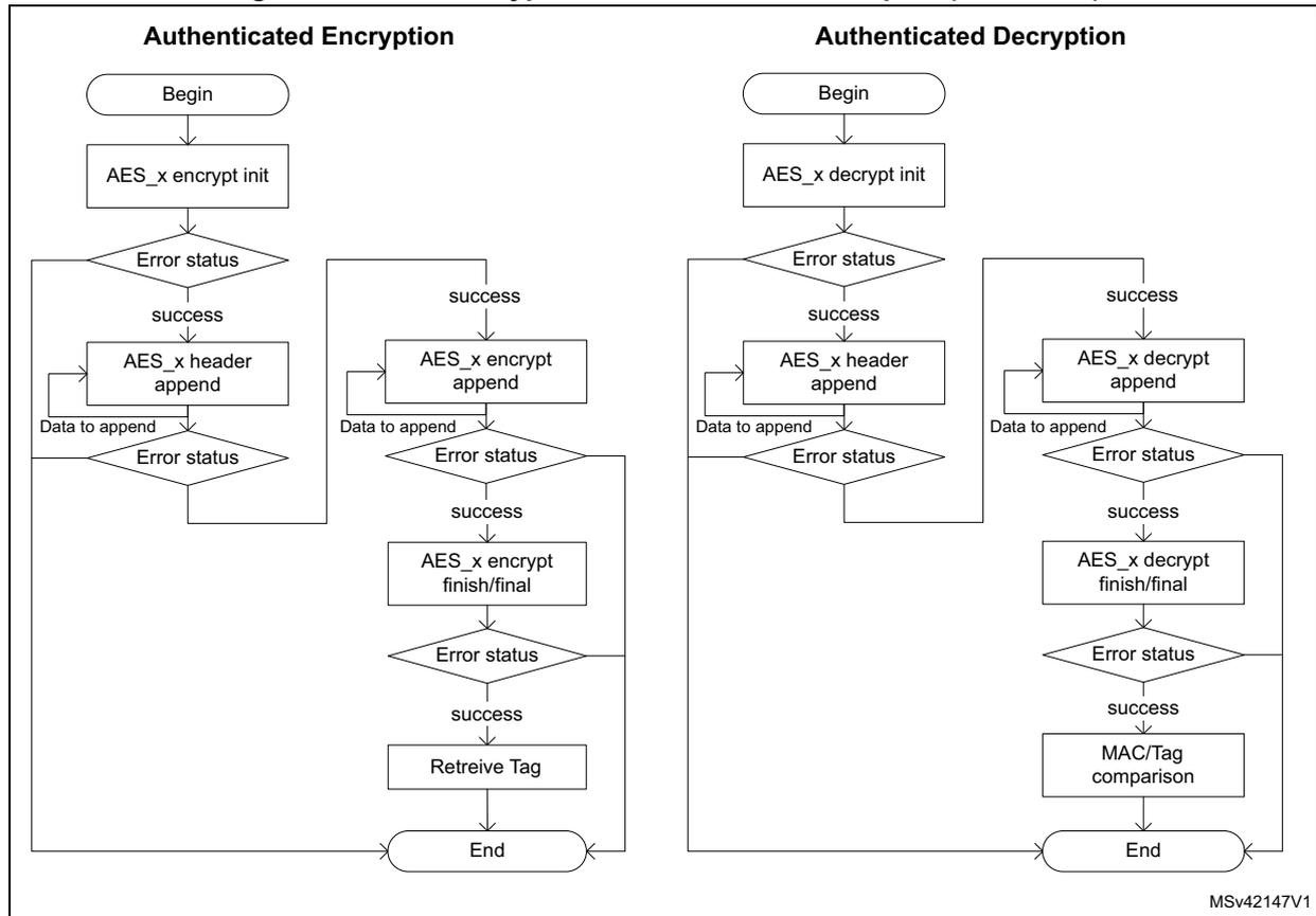
graph TD
    subgraph Authenticated Encryption
        AE_B([Begin]) --> AE_I[AES_x encrypt init]
        AE_I --> AE_ES1{Error status}
        AE_ES1 -- success --> AE_HA[AES_x header append]
        AE_HA -- Data to append --> AE_ES2{Error status}
        AE_ES2 -- success --> AE_AE[AES_x encrypt append]
        AE_AE -- Data to append --> AE_ES3{Error status}
        AE_ES3 -- success --> AE_F[AES_x encrypt finish/final]
        AE_F --> AE_ES4{Error status}
        AE_ES4 -- success --> AE_RT[Retreive Tag]
        AE_RT --> AE_E([End])
        AE_ES1 -- error --> AE_E
        AE_ES2 -- error --> AE_E
        AE_ES3 -- error --> AE_E
        AE_ES4 -- error --> AE_E
    end
    subgraph Authenticated Decryption
        AD_B([Begin]) --> AD_I[AES_x decrypt init]
        AD_I --> AD_ES1{Error status}
        AD_ES1 -- success --> AD_HA[AES_x header append]
        AD_HA -- Data to append --> AD_ES2{Error status}
        AD_ES2 -- success --> AD_AE[AES_x decrypt append]
        AD_AE -- Data to append --> AD_ES3{Error status}
        AD_ES3 -- success --> AD_F[AES_x decrypt finish/final]
        AD_F --> AD_ES4{Error status}
        AD_ES4 -- success --> AD_MTC[MAC/Tag comparison]
        AD_MTC --> AD_E([End])
        AD_ES1 -- error --> AD_E
        AD_ES2 -- error --> AD_E
        AD_ES3 -- error --> AD_E
        AD_ES4 -- error --> AD_E
    end
MSv42147V1
Initialization of AES
To initialize AES, first disable it by clearing the EN bit of the AES_CR register. Then perform the following steps in any order:
- • Configure the AES mode, by programming the MODE[1:0] bitfield of the AES_CR register.
- – For encryption, Mode 1 must be selected (MODE[1:0] = 00).
- – For decryption, Mode 3 must be selected (MODE[1:0] = 10), unless ECB or CBC chaining modes are used. In this latter case, an initial key derivation of the encryption key must be performed, as described in Section 28.4.5: AES decryption key preparation .
- • Select the chaining mode, by programming the CHMOD[2:0] bitfield of the AES_CR register
- • Configure the key size (128-bit or 256-bit), with the KEYSIZE bitfield of the AES_CR register.
- • Write a symmetric key into the AES_KEYRx registers (4 or 8 registers depending on the key size).
- • Configure the data type (1-, 8-, 16- or 32-bit), with the DATATYPE[1:0] bitfield in the AES_CR register.
- • When it is required (for example in CBC or CTR chaining modes), write the initialization vectors into the AES_IVRx register.
Data append
This section describes different ways of appending data for processing, where the size of data to process is not a multiple of 128 bits.
For ECB, CBC and GCM encryption mode, refer to Section 28.4.6: AES ciphertext stealing and data padding . The second-last and the last block management in these cases is more complex than in the sequence described in this section.
Data append through polling
This method uses flag polling to control the data append.
For all other cases, the data is appended through the following sequence:
- 1. Enable the AES peripheral by setting the EN bit of the AES_CR register.
- 2. Repeat the following sub-sequence until the payload is entirely processed:
- a) Write four input data words into the AES_DINR register.
- b) Wait until the status flag CCF is set in the AES_SR, then read the four data words from the AES_DOUTR register.
- c) Clear the CCF flag, by setting the CCFC bit of the AES_CR register.
- d) If the data block just processed is the second-last block of the message and the significant data in the last block to process is inferior to 128 bits, pad the remainder of the last block with zeros
- 3. Discard the data that is not part of the payload, then disable the AES peripheral by clearing the EN bit of the AES_CR register.
Note: Up to three wait cycles are automatically inserted between two consecutive writes to the AES_DINR register, to allow sending the key to the AES processor.
Data append using interrupt
The method uses interrupt from the AES peripheral to control the data append, through the following sequence:
- 1. Enable interrupts from AES by setting the CCFIE bit of the AES_CR register.
- 2. Enable the AES peripheral by setting the EN bit of the AES_CR register.
- 3. Write first four input data words into the AES_DINR register.
- 4. Handle the data in the AES interrupt service routine, upon interrupt:
- a) Read four output data words from the AES_DOUTR register.
- b) Clear the CCF flag and thus the pending interrupt, by setting the CCFC bit of the AES_CR register
- c) If the data block just processed is the second-last block of an message and the significant data in the last block to process is inferior to 128 bits, pad the remainder of the last block with zeros. Then proceed with point 4e).
- d) If the data block just processed is the last block of the message, discard the data that is not part of the payload, then disable the AES peripheral by clearing the EN bit of the AES_CR register and quit the interrupt service routine.
- e) Write next four input data words into the AES_DINR register and quit the interrupt service routine.
Note: AES is tolerant of delays between consecutive read or write operations, which allows, for example, an interrupt from another peripheral to be served between two AES computations.
Data append using DMA
With this method, all the transfers and processing are managed by DMA and AES. To use the method, proceed as follows:
- 1. Prepare the last four-word data block (if the data to process does not fill it completely), by padding the remainder of the block with zeros.
- 2. Configure the DMA controller so as to transfer the data to process from the memory to the AES peripheral input and the processed data from the AES peripheral output to the memory, as described in Section 28.4.16: AES DMA interface . Configure the DMA controller so as to generate an interrupt on transfer completion.
- 3. Enable the AES peripheral by setting the EN bit of the AES_CR register
- 4. Enable DMA requests by setting the DMAINEN and DMAOUTEN bits of the AES_CR register.
- 5. Upon DMA interrupt indicating the transfer completion, get the AES-processed data from the memory.
Note: The CCF flag has no use with this method, because the reading of the AES_DOUTR register is managed by DMA automatically, without any software action, at the end of the computation phase.
28.4.5 AES decryption key preparation
For an ECB or CBC decryption, a key for the first round of decryption must be derived from the key of the last round of encryption. This is why a complete key schedule of encryption is required before performing the decryption. This key preparation is not required for AES decryption in modes other than ECB or CBC.
Recommended method is to select the Mode 2 by setting to 01 the MODE[1:0] bitfield of the AES_CR (key process only), then proceed with the decryption by setting MODE[1:0] to 10 (Mode 3, decryption only). Mode 2 usage is described below:
- 1. Disable the AES peripheral by clearing the EN bit of the AES_CR register.
- 2. Select Mode 2 by setting to 01 the MODE[1:0] bitfield of the AES_CR. The CHMOD[2:0] bitfield is not significant in this case because this key derivation mode is independent of the chaining algorithm selected.
- 3. Set key length to 128 or 256 bits, via KEYSIZE bit of AES_CR register.
- 4. Write the AES_KEYRx registers (128 or 256 bits) with encryption key, as shown in Figure 199 . Writes to the AES_IVRx registers have no effect.
- 5. Enable the AES peripheral, by setting the EN bit of the AES_CR register.
- 6. Wait until the CCF flag is set in the AES_SR register.
- 7. Derived key is available in AES core, ready to use for decryption. Application can also read the AES_KEYRx register to obtain the derived key if needed, as shown in Figure 199 (the processed key is loaded automatically into the AES_KEYRx registers).
Note: The AES is disabled by hardware when the derivation key is available.
To restart a derivation key computation, repeat steps 4, 5, 6 and 7.
Figure 199. Encryption key derivation for ECB/CBC decryption (Mode 2)
![Figure 199. Encryption key derivation for ECB/CBC decryption (Mode 2). The diagram shows a sequence of operations: Input phase (4 write operations into AES_KEYRx[31:0] with WR EK3, WR EK2, WR EK1, WR EK0), Computation phase (Wait until flag CCF = 1, with EN = 1 into AES_CR), and Output phase (optional, 4 read operations of AES_KEYRx[31:0] with RD DK3, RD DK2, RD DK1, RD DK0). The input phase is labeled MSB to LSB, and the output phase is also labeled MSB to LSB. A note indicates that EK = encryption key = 4 words (EK3, ..., EK0) and DK = decryption key = 4 words (DK3, ..., DK0). The diagram is labeled MS18937V2.](/RM0351-STM32L47-48-49-4A/7b6343da2947b9ee07599a49ae19311a_img.jpg)
The diagram illustrates the key derivation process for ECB/CBC decryption (Mode 2). It is divided into three main phases:
- Input phase:
4 write operations into
AES_KEYRx[31:0]. The words areWR EK3(MSB),WR EK2,WR EK1, andWR EK0(LSB). - Computation phase:
Wait until flag
CCF = 1. This phase is triggered by settingEN = 1intoAES_CR. - Output phase (optional):
4 read operations of
AES_KEYRx[31:0]. The words areRD DK3(MSB),RD DK2,RD DK1, andRD DK0(LSB). The 128-bit derivation key is stored intoAES_KEYRx.
EK = encryption key = 4 words (EK3, ..., EK0)
DK = decryption key = 4 words (DK3, ..., DK0)
MS18937V2
If the software stores the initial key prepared for decryption, it is enough to do the key schedule operation only once for all the data to be decrypted with a given cipher key.
Note: The operation of the key preparation lasts 80 or 109 clock cycles, depending on the key size (128- or 256-bit).
Note:
Alternative key preparation is to select Mode 4 by setting to 11 the
MODE[1:0]
bitfield of the
AES_CR
register. In this case Mode 3 cannot be used.
28.4.6 AES ciphertext stealing and data padding
When using AES in ECB or CBC modes to manage messages the size of which is not a multiple of the block size (128 bits), ciphertext stealing techniques are used, such as those described in NIST Special Publication 800-38A, Recommendation for Block Cipher Modes of Operation: Three Variants of Ciphertext Stealing for CBC Mode . Since the AES peripheral on the device does not support such techniques, the last two blocks of input data must be handled in a special way by the application.
Note: Ciphertext stealing techniques are not documented in this reference manual.
Similarly, when AES is used in other modes than ECB or CBC, an incomplete input data block (that is, block with input data shorter than 128 bits) must be padded with zeros prior to encryption (that is, extra bits must be appended to the trailing end of the data string). After decryption, the extra bits must be discarded. As AES does not implement automatic data padding operation to the last block , the application must follow the recommendation given in Section 28.4.4: AES procedure to perform a cipher operation on page 828 to manage messages the size of which is not a multiple of 128 bits.
Note:
Padding data are swapped in a similar way as normal data, according to the
DATATYPE[1:0]
field of the
AES_CR
register (see
Section 28.4.13: .AES data registers and data swapping on page 854
for details).
A workaround is required in order to properly compute authentication tags for GCM encryption , when the input data in the last block is inferior to 128 bits . During GCM encryption payload phase and before inserting a last plaintext block smaller than 128 bits, then application must apply the following steps:
- 1. Disable the AES peripheral by clearing the EN bit of the AES_CR register
- 2. Change the mode to CTR by writing 010 to the CHMOD[2:0] bitfield of the AES_CR register.
- 3. Pad the last block (smaller than 128 bits) with zeros to have a complete block of 128 bits, then write it into AES_DINR register.
- 4. Upon encryption completion, read the 128-bit ciphertext from the AES_DOUTR register and store it as intermediate data.
- 5. Change again the mode to GCM by writing 011 to the CHMOD[2:0] bitfield of the AES_CR register.
- 6. Select Final phase by writing 11 to the GCMPH[1:0] bitfield of the AES_CR register.
- 7. In the intermediate data, set to zero the bits corresponding to the padded bits of the last block of payload, then insert the resulting data into AES_DINR register.
- 8. Wait for operation completion, and read data on AES_DOUTR. This data is to be discarded.
- 9. Apply the normal Final phase as described in Section 28.4.10: AES Galois/counter mode (GCM) on page 842
28.4.7 AES task suspend and resume
A message can be suspended if another message with a higher priority must be processed. When this highest priority message is sent, the suspended message can resume in both encryption or decryption mode.
Suspend/resume operations do not break the chaining operation and the message processing can resume as soon as AES is enabled again to receive the next data block.
Figure 200 gives an example of suspend/resume operation: Message 1 is suspended in order to send a shorter and higher-priority Message 2.
Figure 200. Example of suspend mode management
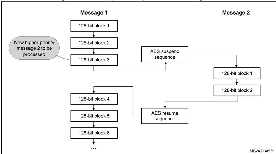
The diagram shows two message processing paths. Message 1 starts with '128-bit block 1', followed by '128-bit block 2', and '128-bit block 3'. After block 3, an arrow points to a box labeled 'AES suspend sequence'. From this box, an arrow points to the start of Message 2. Message 2 consists of '128-bit block 1' and '128-bit block 2'. After block 2, an arrow points to a box labeled 'AES resume sequence'. From this box, an arrow points back to the continuation of Message 1, which shows '128-bit block 4', '128-bit block 5', and '128-bit block 6', followed by an ellipsis. A callout bubble on the left points to the transition between Message 1 and Message 2, containing the text 'New higher-priority message 2 to be processed'. The diagram is labeled 'MSv42148V1' in the bottom right corner.
A detailed description of suspend/resume operations is in the sections dedicated to each AES mode.
28.4.8 AES basic chaining modes (ECB, CBC)
Overview
This section gives a brief explanation of the four basic operation modes provided by the AES computing core: ECB encryption, ECB decryption, CBC encryption and CBC decryption. For detailed information, refer to the FIPS publication 197 from November 26, 2001.
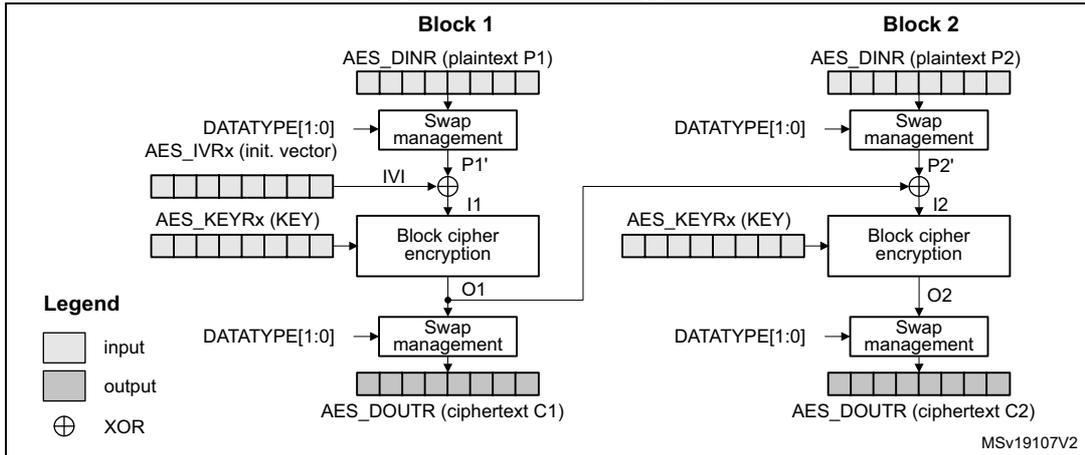
Figure 201 illustrates the electronic codebook (ECB) encryption.
![Diagram of ECB encryption showing two parallel processing paths for Block 1 and Block 2. Each path starts with AES_DINR (plaintext), goes through Swap management (controlled by DATATYPE[1:0]), then an Encrypt block (using AES_KEYRx), then another Swap management block, and ends at AES_DOUTR (ciphertext).](/RM0351-STM32L47-48-49-4A/0a2f8f26374399333950d95d7cd5559f_img.jpg)
Figure 201. ECB encryption
The diagram shows the encryption flow for two blocks.
- Block 1: Plaintext P1 enters AES_DINR , undergoes Swap management (DATATYPE[1:0]) to become I1 , is processed by the Encrypt block (using AES_KEYRx ) to become O1 , undergoes another Swap management , and is output as ciphertext C1 in AES_DOUTR .
- Block 2: Plaintext P2 follows the same path through AES_DINR , Swap management (I2), Encrypt (O2), and Swap management to become ciphertext C2 in AES_DOUTR .
In ECB encrypt mode, the 128-bit plaintext input data block \( P_x \) in the AES_DINR register first goes through bit/byte/half-word swapping. The swap result \( I_x \) is processed with the AES core set in encrypt mode, using a 128- or 256-bit key. The encryption result \( O_x \) goes through bit/byte/half-word swapping, then is stored in the AES_DOUTR register as 128-bit ciphertext output data block \( C_x \) . The ECB encryption continues in this way until the last complete plaintext block is encrypted.
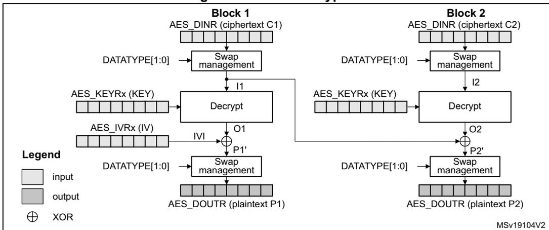
Figure 202 illustrates the electronic codebook (ECB) decryption.
![Diagram of ECB decryption showing two parallel processing paths for Block 1 and Block 2. Each path starts with AES_DINR (ciphertext), goes through Swap management (controlled by DATATYPE[1:0]), then a Decrypt block (using AES_KEYRx), then another Swap management block, and ends at AES_DOUTR (plaintext).](/RM0351-STM32L47-48-49-4A/6e43883331f53f650df5d2d080e7c487_img.jpg)
Figure 202. ECB decryption
The diagram shows the decryption flow for two blocks.
- Block 1: Ciphertext C1 enters AES_DINR , undergoes Swap management (DATATYPE[1:0]) to become I1 , is processed by the Decrypt block (using AES_KEYRx ) to become O1 , undergoes another Swap management , and is output as plaintext P1 in AES_DOUTR .
- Block 2: Ciphertext C2 follows the same path through AES_DINR , Swap management (I2), Decrypt (O2), and Swap management to become plaintext P2 in AES_DOUTR .
To perform an AES decryption in the ECB mode, the secret key has to be prepared by collecting the last-round encryption key (which requires to first execute the complete key schedule for encryption), and using it as the first-round key for the decryption of the ciphertext. This preparation is supported by the AES core.
In ECB decrypt mode, the 128-bit ciphertext input data block C1 in the AES_DINR register first goes through bit/byte/half-word swapping. The keying sequence is reversed compared to that of the ECB encryption. The swap result I1 is processed with the AES core set in decrypt mode, using the formerly prepared decryption key. The decryption result goes through bit/byte/half-word swapping, then is stored in the AES_DOUTR register as 128-bit plaintext output data block P1. The ECB decryption continues in this way until the last complete ciphertext block is decrypted.
Figure 203 illustrates the cipher block chaining (CBC) encryption mode.
Figure 203. CBC encryption
In CBC encrypt mode, the first plaintext input block, after bit/byte/half-word swapping (P1'), is XOR-ed with a 128-bit IVI bitfield (initialization vector and counter), producing the I1 input data for encrypt with the AES core, using a 128- or 256-bit key. The resulting 128-bit output block O1, after swapping operation, is used as ciphertext C1. The O1 data is then XOR-ed with the second-block plaintext data P2' to produce the I2 input data for the AES core to produce the second block of ciphertext data. The chaining of data blocks continues in this way until the last plaintext block in the message is encrypted.
If the message size is not a multiple of 128 bits, the final partial data block is encrypted in the way explained in Section 28.4.6: AES ciphertext stealing and data padding .
Figure 204 illustrates the cipher block chaining (CBC) decryption mode.
Figure 204. CBC decryption
In CBC decrypt mode, like in ECB decrypt mode, the secret key must be prepared to perform an AES decryption.
After the key preparation process, the decryption goes as follows: the first 128-bit ciphertext block (after the swap operation) is used directly as the AES core input block I1 for decrypt operation, using the 128-bit or 256-bit key. Its output O1 is XOR-ed with the 128-bit IVI field (that must be identical to that used during encryption) to produce the first plaintext block P1.
The second ciphertext block is processed in the same way as the first block, except that the I1 data from the first block is used in place of the initialization vector.
The decryption continues in this way until the last complete ciphertext block is decrypted.
If the message size is not a multiple of 128 bits, the final partial data block is decrypted in the way explained in Section 28.4.6: AES ciphertext stealing and data padding .
For more information on data swapping, refer to Section 28.4.13: .AES data registers and data swapping .
ECB/CBC encryption sequence
The sequence of events to perform an ECB/CBC encryption (more detail in Section 28.4.4 ):
- 1. Disable the AES peripheral by clearing the EN bit of the AES_CR register.
- 2. Select the Mode 1 by to 00 the MODE[1:0] bitfield of the AES_CR register and select ECB or CBC chaining mode by setting the CHMOD[2:0] bitfield of the AES_CR register to 000 or 001, respectively. Data type can also be defined, using DATATYPE[1:0] bitfield.
- 3. Select 128- or 256-bit key length through the KEYSIZE bit of the AES_CR register.
- 4. Write the AES_KEYRx registers (128 or 256 bits) with encryption key. Fill the AES_IVRx registers with the initialization vector data if CBC mode has been selected.
- 5. Enable the AES peripheral by setting the EN bit of the AES_CR register.
- 6. Write the AES_DINR register four times to input the plaintext (MSB first), as shown in Figure 205 .
- 7. Wait until the CCF flag is set in the AES_SR register.
- 8. Read the AES_DOUTR register four times to get the ciphertext (MSB first) as shown in Figure 205 . Then clear the CCF flag by setting the CCFC bit of the AES_CR register.
- 9. Repeat steps 6,7,8 to process all the blocks with the same encryption key.
Figure 205. ECB/CBC encryption (Mode 1)
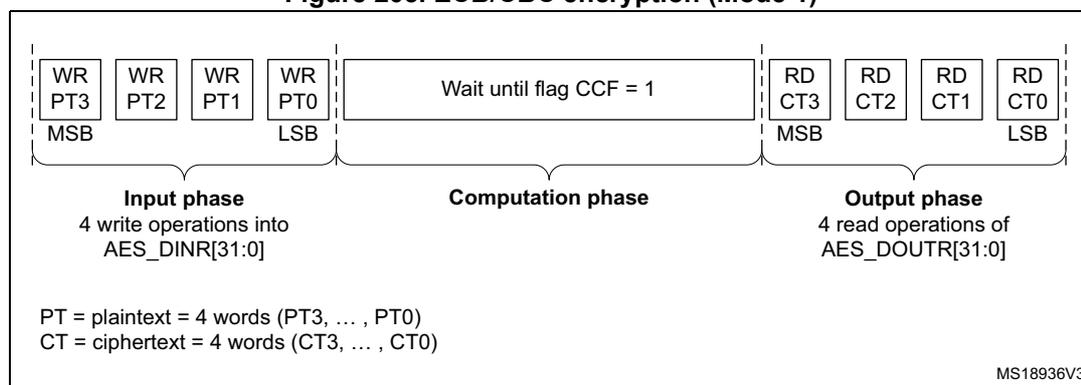
The diagram illustrates the sequence of operations for ECB/CBC encryption (Mode 1) across three phases:
- Input phase: Four write operations into the AES_DINR[31:0] register. The plaintext words are written in order: PT3 (MSB), PT2, PT1, and PT0 (LSB).
- Computation phase: A period where the user waits until the CCF flag is set to 1.
- Output phase: Four read operations from the AES_DOUTR[31:0] register. The ciphertext words are read in order: CT3 (MSB), CT2, CT1, and CT0 (LSB).
Legend:
PT = plaintext = 4 words (PT3, ..., PT0)
CT = ciphertext = 4 words (CT3, ..., CT0)
Reference: MS18936V3
ECB/CBC decryption sequence
The sequence of events to perform an AES ECB/CBC decryption is as follows (more detail in Section 28.4.4 ):
- 1. Follow the steps described in Section 28.4.5: AES decryption key preparation on page 832 , in order to prepare the decryption key in AES core.
- 2. Disable the AES peripheral by clearing the EN bit of the AES_CR register.
- 3. Select the Mode 3 by setting to 10 the MODE[1:0] bitfield of the AES_CR register and select ECB or CBC chaining mode by setting the CHMOD[2:0] bitfield of the AES_CR register to 000 or 001, respectively. Data type can also be defined, using DATATYPE[1:0] bitfield.
- 4. Select key length of 128 or 256 bits via KEYSIZE bitfield of the AES_CR register.
- 5. Write the AES_IVRx registers with the initialization vector (required in CBC mode only).
- 6. Enable AES by setting the EN bit of the AES_CR register.
- 7. Write the AES_DINR register four times to input the cipher text (MSB first), as shown in Figure 206 .
- 8. Wait until the CCF flag is set in the AES_SR register.
- 9. Read the AES_DOUTR register four times to get the plain text (MSB first), as shown in Figure 206 . Then clear the CCF flag by setting the CCFC bit of the AES_CR register.
- 10. Repeat steps 7,8,9 to process all the blocks encrypted with the same key.
Figure 206. ECB/CBC decryption (Mode 3)
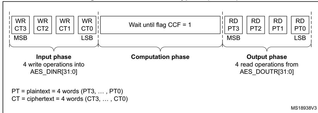
The diagram illustrates the sequence of operations for ECB/CBC decryption in Mode 3. It is divided into three main phases:
- Input phase: Labeled "4 write operations into AES_DINR[31:0]". It shows four write operations (WR) into the AES_DINR register. The data is written in four words: CT3, CT2, CT1, and CT0. CT3 is the Most Significant Byte (MSB) and CT0 is the Least Significant Byte (LSB).
- Computation phase: Labeled "Wait until flag CCF = 1". This phase occurs after the input phase and before the output phase.
- Output phase: Labeled "4 read operations from AES_DOUTR[31:0]". It shows four read operations (RD) from the AES_DOUTR register. The data is read in four words: PT3, PT2, PT1, and PT0. PT3 is the MSB and PT0 is the LSB.
Legend:
PT = plaintext = 4 words (PT3, ... , PT0)
CT = ciphertext = 4 words (CT3, ... , CT0)
Reference: MS18938V3
Suspend/resume operations in ECB/CBC modes
To suspend the processing of a message, proceed as follows:
- 1. If DMA is used, stop the AES DMA transfers to the IN FIFO by clearing the MAINEN bit of the AES_CR register.
- 2. If DMA is not used, read four times the AES_DOUTR register to save the last processed block. If DMA is used, wait until the CCF flag is set in the AES_SR register
then stop the DMA transfers from the OUT FIFO by clearing the DMAOUTEN bit of the AES_CR register.
- 1. If DMA is not used, poll the CCF flag of the AES_SR register until it becomes 1 (computation completed).
- 2. Clear the CCF flag by setting the CCFC bit of the AES_CR register.
- 3. Save initialization vector registers (only required in CBC mode as AES_IVRx registers are altered during the data processing).
- 4. Disable the AES peripheral by clearing the bit EN of the AES_CR register.
- 5. Save the current AES configuration in the memory (except AES initialization vector values).
- 6. If DMA is used, save the DMA controller status (pointers for IN and OUT data transfers, number of remaining bytes, and so on).
Note: In point 7, the derived key information stored in AES_KEYRx registers can optionally be saved in memory if the interrupted process is a decryption. Otherwise those registers do not need to be saved as the original key value is known by the application
To resume the processing of a message , proceed as follows:
- 1. If DMA is used, configure the DMA controller so as to complete the rest of the FIFO IN and FIFO OUT transfers.
- 2. Ensure that AES is disabled (the EN bit of the AES_CR must be 0).
- 3. Restore the AES_CR and AES_KEYRx register setting, using the values of the saved configuration. In case of decryption, derived key information can be written in AES_KEYRx register instead of the original key value.
- 4. Prepare the decryption key as described in Section 28.4.5: AES decryption key preparation (only required for ECB or CBC decryption). This step is not necessary if derived key information has been loaded in AES_KEYRx registers.
- 5. Restore AES_IVRx registers using the saved configuration (only required in CBC mode).
- 6. Enable the AES peripheral by setting the EN bit of the AES_CR register.
- 7. If DMA is used, enable AES DMA transfers by setting the DMAINEN and DMAOUTEN bits of the AES_CR register.
Alternative single ECB/CBC decryption using Mode 4
The sequence of events to perform a single round of ECB/CBC decryption using Mode 4 is:
- 1. Disable the AES peripheral by clearing the EN bit of the AES_CR register.
- 2. Select the Mode 4 by setting to 11 the MODE[1:0] bitfield of the AES_CR register and select ECB or CBC chaining mode by setting the CHMOD[2:0] bitfield of the AES_CR register to 000 or 001, respectively.
- 3. Select key length of 128 or 256 bits via KEYSIZE bitfield of the AES_CR register.
- 4. Write the AES_KEYRx registers with the encryption key. Write the AES_IVRx registers if the CBC mode is selected.
- 5. Enable the AES peripheral by setting the EN bit of the AES_CR register.
- 6. Write the AES_DINR register four times to input the cipher text (MSB first).
- 7. Wait until the CCF flag is set in the AES_SR register.
- 8. Read the AES_DOUTR register four times to get the plain text (MSB first). Then clear the CCF flag by setting the CCFC bit of the AES_CR register.
Note: When mode 4 is selected mode 3 cannot be used.
In mode 4, the AES_KEYRx registers contain the encryption key during all phases of the processing. No derivation key is stored in these registers. It is stored internally in AES.
28.4.9 AES counter (CTR) mode
Overview
The counter mode (CTR) uses AES as a key-stream generator. The generated keys are then XOR-ed with the plaintext to obtain the ciphertext.
CTR chaining is defined in NIST Special Publication 800-38A, Recommendation for Block Cipher Modes of Operation . A typical message construction in CTR mode is given in Figure 207 .
Figure 207. Message construction in CTR mode
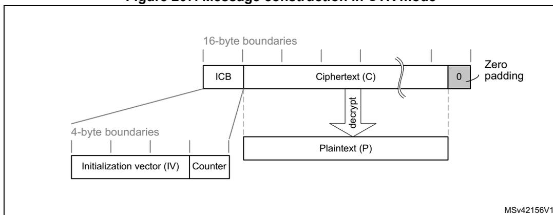
The diagram illustrates the message construction in CTR mode. At the top, a horizontal bar represents the message structure, divided into 16-byte boundaries. The first 16-byte block is the Initial Counter Block (ICB). This is followed by the Ciphertext (C), which is shown as a series of blocks. The last block of the ciphertext is followed by a '0' representing zero padding. Below the ICB, a callout shows its internal structure: it is composed of two fields, 'Initialization vector (IV)' and 'Counter', each with 4-byte boundaries. A vertical arrow labeled 'decrypt' points from the Ciphertext (C) block to a 'Plaintext (P)' block, indicating the decryption process.
The structure of this message is:
- • A 16-byte initial counter block (ICB), composed of two distinct fields:
- – Initialization vector (IV) : a 96-bit value that must be unique for each encryption cycle with a given key.
- – Counter : a 32-bit big-endian integer that is incremented each time a block processing is completed. The initial value of the counter should be set to 1.
- • The plaintext P is encrypted as ciphertext C, with a known length. This length can be non-multiple of 16 bytes, in which case a plaintext padding is required.
CTR encryption and decryption
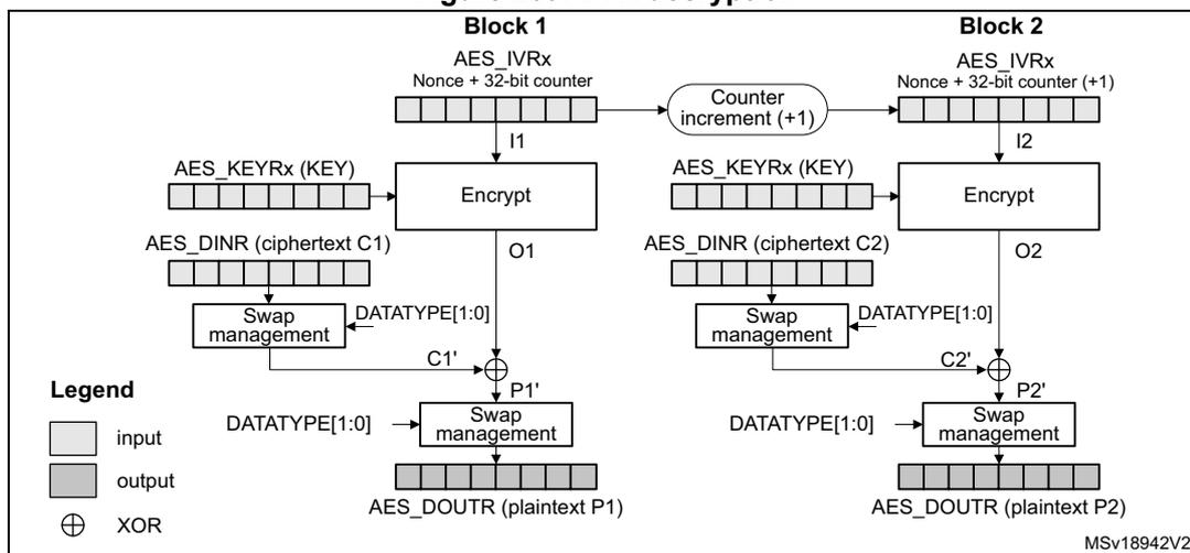
Figure 208 and Figure 209 describe the CTR encryption and decryption process, respectively, as implemented in the AES peripheral. The CTR mode is selected by writing 010 to the CHMOD[2:0] bitfield of AES_CR register.
Figure 208. CTR encryption
Block 1
AES_IVRx (IV + 32-bit counter)
I1
AES_KEYRx (KEY)
Encrypt
O1
AES_DINR (plaintext P1)
Swap management
DATATYPE[1:0]
P1'
XOR
C1'
Swap management
DATATYPE[1:0]
AES_DOUTr (ciphertext C1)
Block 2
Counter increment (+1)
AES_IVRx (Nonce + 32-bit counter (+1))
I2
AES_KEYRx (KEY)
Encrypt
O2
AES_DINR (plaintext P2)
Swap management
DATATYPE[1:0]
P2'
XOR
C2'
Swap management
DATATYPE[1:0]
AES_DOUTr (ciphertext C2)
Legend
input
output
XOR
MSv19102V2
Figure 209. CTR decryption
Block 1
AES_IVRx (Nonce + 32-bit counter)
I1
AES_KEYRx (KEY)
Encrypt
O1
AES_DINR (ciphertext C1)
Swap management
DATATYPE[1:0]
C1'
XOR
P1'
Swap management
DATATYPE[1:0]
AES_DOUTr (plaintext P1)
Block 2
Counter increment (+1)
AES_IVRx (Nonce + 32-bit counter (+1))
I2
AES_KEYRx (KEY)
Encrypt
O2
AES_DINR (ciphertext C2)
Swap management
DATATYPE[1:0]
C2'
XOR
P2'
Swap management
DATATYPE[1:0]
AES_DOUTr (plaintext P2)
Legend
input
output
XOR
MSv18942V2
In CTR mode, the cryptographic core output (also called keystream) \( O_x \) is XOR-ed with relevant input block ( \( P_x' \) for encryption, \( C_x' \) for decryption), to produce the correct output block ( \( C_x' \) for encryption, \( P_x' \) for decryption). Initialization vectors in AES must be initialized as shown in Table 180 .
Table 180. CTR mode initialization vector definition
| AES_IVR3[31:0] | AES_IVR2[31:0] | AES_IVR1[31:0] | AES_IVR0[31:0] |
|---|---|---|---|
| Nonce[31:0] | Nonce[63:32] | Nonce[95:64] | 32-bit counter = 0x0001 |
Unlike in CBC mode that uses the AES_IVRx registers only once when processing the first data block, in CTR mode AES_IVRx registers are used for processing each data block, and the AES peripheral increments the counter bits of the initialization vector (leaving the nonce bits unchanged).
CTR decryption does not differ from CTR encryption, since the core always encrypts the current counter block to produce the key stream that is then XOR-ed with the plaintext (CTR
encryption) or ciphertext (CTR decryption) input. In CTR mode, the MODE[1:0] bitfield settings 11, 10 or 00 default all to encryption mode, and the setting 01 (key derivation) is forbidden.
The sequence of events to perform an encryption or a decryption in CTR chaining mode:
- 1. Ensure that AES is disabled (the EN bit of the AES_CR must be 0).
- 2. Select CTR chaining mode by setting to 010 the CHMOD[2:0] bitfield of the AES_CR register. Set MODE[1:0] bitfield to any value other than 01.
- 3. Initialize the AES_KEYRx registers, and load the AES_IVRx registers as described in Table 180 .
- 4. Set the EN bit of the AES_CR register, to start encrypting the current counter (EN is automatically reset when the calculation finishes).
- 5. If it is the last block, pad the data with zeros to have a complete block, if needed.
- 6. Append data in AES, and read the result. The three possible scenarios are described in Section 28.4.4: AES procedure to perform a cipher operation .
- 7. Repeat the previous step till the second-last block is processed. For the last block, apply the two previous steps and discard the bits that are not part of the payload (if the size of the significant data in the last input block is less than 16 bytes).
Suspend/resume operations in CTR mode
Like for the CBC mode, it is possible to interrupt a message to send a higher priority message, and resume the message that was interrupted. Detailed CBC suspend/resume sequence is described in Section 28.4.8: AES basic chaining modes (ECB, CBC) .
Note: Like for CBC mode, the AES_IVRx registers must be reloaded during the resume operation.
28.4.10 AES Galois/counter mode (GCM)
Overview
The AES Galois/counter mode (GCM) allows encrypting and authenticating a plaintext message into the corresponding ciphertext and tag (also known as message authentication code). To ensure confidentiality, GCM algorithm is based on AES counter mode. It uses a multiplier over a fixed finite field to generate the tag.
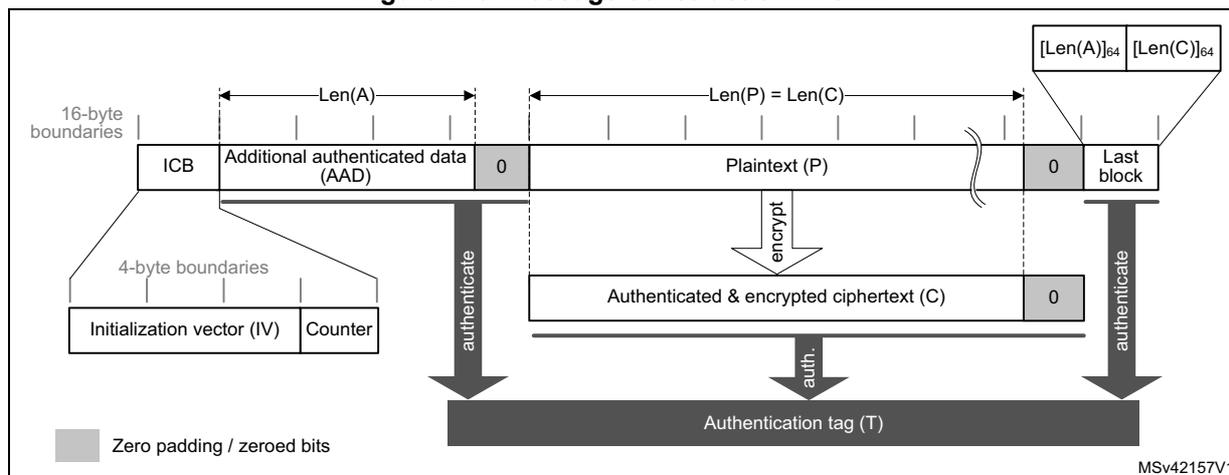
GCM chaining is defined in NIST Special Publication 800-38D, Recommendation for Block Cipher Modes of Operation - Galois/Counter Mode (GCM) and GMAC . A typical message construction in GCM mode is given in Figure 210 .
Figure 210. Message construction in GCM
The diagram illustrates the message construction process in GCM. It shows the following components and flow:
- ICB (Initial Counter Block): A 16-byte block composed of a 96-bit Initialization vector (IV) and a 32-bit Counter . It is used for authentication.
- Additional authenticated data (AAD): A variable-length block of length \( Len(A) \) . It is also used for authentication.
- Plaintext (P): A variable-length block of length \( Len(P) = Len(C) \) . It is both encrypted and authenticated.
- Authenticated & encrypted ciphertext (C): The result of encrypting the plaintext. It has the same length as the plaintext.
- Authentication tag (T): A 128-bit tag generated from the ICB, AAD, and ciphertext. It is used for verification.
- Last block: The final block of the message, containing length information for the AAD and the payload. It is shown as a 128-bit block with two 64-bit length fields: \( [Len(A)]_{64} \) and \( [Len(C)]_{64} \) .
Arrows indicate the flow: ICB and AAD are input to the authenticate function. Plaintext (P) is input to the encrypt function to produce ciphertext (C). Ciphertext (C) and the Last block are input to the auth. function to produce the Authentication tag (T).
Legend: Gray boxes represent zero padding / zeroed bits.
The message has the following structure:
- •
16-byte initial counter block (ICB)
, composed of two distinct fields:
- – Initialization vector (IV): a 96-bit value that must be unique for each encryption cycle with a given key. Note that the GCM standard supports IVs with less than 96 bits, but in this case strict rules apply.
- – Counter: a 32-bit big-endian integer that is incremented each time a block processing is completed. According to NIST specification, the counter value is 0x2 when processing the first block of payload.
- • Authenticated header AAD (also knows as additional authentication data) has a known length \( Len(A) \) that may be a non-multiple of 16 bytes, and must not exceed \( 2^{64} - 1 \) bits. This part of the message is only authenticated, not encrypted.
- • Plaintext message P is both authenticated and encrypted as ciphertext C, with a known length \( Len(P) \) that may be non-multiple of 16 bytes, and cannot exceed \( 2^{32} - 2 \) 128-bit blocks.
- • Last block contains the AAD header length (bits [32:63]) and the payload length (bits [96:127]) information, as shown in Table 181 .
The GCM standard specifies that ciphertext C has the same bit length as the plaintext P.
When a part of the message (AAD or P) has a length that is a non-multiple of 16-bytes a special padding scheme is required.
Table 181. GCM last block definition
| Endianness | Bit[0] ---------- Bit[31] | Bit[32]---------- Bit[63] | Bit[64] ---------- Bit[95] | Bit[96] ---------- Bit[127] |
|---|---|---|---|---|
| Input data | 0x0 | AAD length[31:0] | 0x0 | Payload length[31:0] |
GCM processing
Figure 211 describes the GCM implementation in the AES peripheral. The GCM is selected by writing 011 to the CHMOD[2:0] bitfield of the AES_CR register.
Figure 211. GCM authenticated encryption
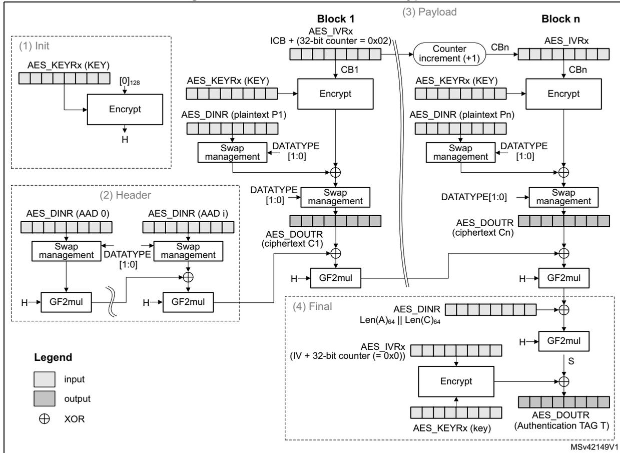
The diagram illustrates the GCM authenticated encryption process, divided into four main stages:
- (1) Init: The process starts with AES_KEYRx (KEY) input to an Encrypt block, which outputs H . This H value is used as input to a GF2mul block.
- (2) Header: AES_DINR (AAD 0) and AES_DINR (AAD i) are processed through Swap management blocks with DATATYPE [1:0] settings. The outputs are then processed by GF2mul blocks using the H value. The results are XORed together.
- (3) Payload:
This stage involves multiple blocks, from
Block 1
to
Block n
.
- Block 1: AES_DINR (plaintext P1) is processed through Swap management with DATATYPE [1:0] . The output is XORed with the counter block CB1 (derived from ICB + (32-bit counter = 0x02) via AES_IVRx ). This result is then processed by Encrypt using AES_KEYRx (KEY) to produce ciphertext C1 . C1 is processed through Swap management with DATATYPE [1:0] to produce AES_DOUTR (ciphertext C1) . This ciphertext is then processed by GF2mul using H and XORed with the output from the Header stage.
- Block n: Similar to Block 1, but the counter block is CBn , which is derived from the previous counter block via a Counter increment (+1) function and AES_IVRx .
- (4) Final: The final stage calculates the authentication tag T . It takes AES_DINR (Len(A)64 || Len(C)64) and processes it through GF2mul using H and XORs it with the accumulated payload authentication value S . The result is processed by Encrypt using AES_IVRx (IV + 32-bit counter (= 0x0)) and AES_KEYRx (key) to produce the final AES_DOUTR (Authentication TAG T) .
Legend:
- input (light gray rectangle)
- output (dark gray rectangle)
- XOR (circle with cross)
MSv42149V1
The mechanism for the confidentiality of the plaintext in GCM mode is similar to that in the Counter mode, with a particular increment function (denoted 32-bit increment) that generates the sequence of input counter blocks.
AES_IVRx registers keeping the counter block of data are used for processing each data block. The AES peripheral automatically increments the Counter[31:0] bitfield. The first counter block (CB1) is derived from the initial counter block ICB by the application software (see Table 182).
Table 182. GCM mode IVI bitfield initialization
| Register | AES_IVR3[31:0] | AES_IVR2[31:0] | AES_IVR1[31:0] | AES_IVR0[31:0] |
|---|---|---|---|---|
| Input data | ICB[31:0] | ICB[63:32] | ICB[95:64] | Counter[31:0] = 0x2 |
Note: In GCM mode, the settings 01 and 11 of the MODE[1:0] bitfield are forbidden.
The authentication mechanism in GCM mode is based on a hash function called GF2mul that performs multiplication by a fixed parameter, called hash subkey (H), within a binary Galois field.
A GCM message is processed through the following phases, further described in next subsections:
- • Init phase: AES prepares the GCM hash subkey (H).
- • Header phase: AES processes the additional authenticated data (AAD), with hash computation only.
- • Payload phase: AES processes the plaintext (P) with hash computation, counter block encryption and data XOR-ing. It operates in a similar way for ciphertext (C).
- • Final phase: AES generates the authenticated tag (T) using the last block of the message.
GCM init phase
During this first step, the GCM hash subkey (H) is calculated and saved internally, to be used for processing all the blocks. The recommended sequence is:
- 1. Ensure that AES is disabled (the EN bit of the AES_CR must be 0).
- 2. Select GCM chaining mode, by setting to 011 the CHMOD[2:0] bitfield of the AES_CR register, and set to 00 (no data swapping) the DATATYPE[1:0] bitfield.
- 3. Indicate the Init phase, by setting to 00 the GCMPH[1:0] bitfield of the AES_CR register.
- 4. Set the MODE[1:0] bitfield of the AES_CR register to 00 or 10.
- 5. Initialize the AES_KEYRx registers with a key, and initialize AES_IVRx registers with the information as defined in Table 182 .
- 6. Start the calculation of the hash key, by setting to 1 the EN bit of the AES_CR register (EN is automatically reset when the calculation finishes).
- 7. Wait until the end of computation, indicated by the CCF flag of the AES_SR transiting to 1. Alternatively, use the corresponding interrupt.
- 8. Clear the CCF flag of the AES_SR register, by setting to 1 the CCFC bit of the AES_CR register, and optionally set the data type (1-, 8- or 16-bit) using the DATATYPE[1:0] bitfield.
GCM header phase
This phase coming after the GCM Init phase must be completed before the payload phase. The sequence to execute, identical for encryption and decryption, is:
- 1. Indicate the header phase, by setting to 01 the GCMPH[1:0] bitfield of the AES_CR register. Do not modify the MODE[1:0] bitfield as set in the Init phase.
- 2. Enable the AES peripheral by setting the EN bit of the AES_CR register.
- 3. If it is the last block and the AAD size in the block is inferior to 128 bits, pad the remainder of the block with zeros. Then append the data block into AES in one of ways described in Section 28.4.4: AES procedure to perform a cipher operation on page 828 .
- 4. Repeat the step 3 until the last additional authenticated data block is processed.
Note: The header phase can be skipped if there is no AAD, that is, Len(A) = 0.
GCM payload phase
This phase, identical for encryption and decryption, is executed after the GCM header phase. During this phase, the encrypted/decrypted payload is stored in the AES_DOUTR register. The sequence to execute is:
- 1. If the header phase was skipped, enable the AES peripheral by setting the EN bit of the AES_CR register.
- 2. Indicate the payload phase, by setting to 10 the GCMPH[1:0] bitfield of the AES_CR register. Do not modify the MODE[1:0] bitfield as set in the Init phase.
- 3. If it is the last block and the plaintext (encryption) or ciphertext (decryption) size in the block is inferior to 128 bits, pad the remainder of the block with zeros.
- 4. Append the data block into AES in one of ways described in Section 28.4.4: AES procedure to perform a cipher operation on page 828 , and read the result.
- 5. Repeat the previous step till the second-last plaintext block is encrypted or till the last block of ciphertext is decrypted. For the last block of plaintext (encryption only), execute the two previous steps. For the last block, discard the bits that are not part of the payload when the last block size is less than 16 bytes.
Note: The payload phase can be skipped if there is no payload data, that is, Len(C) = 0 (see GMAC mode).
GCM final phase
In this last phase, the AES peripheral generates the GCM authentication tag and stores it in the AES_DOUTR register. The sequence to execute is:
- 1. Indicate the final phase, by setting to 11 the GCMPH[1:0] bitfield of the AES_CR register. Select encrypt mode by setting to 00 the MODE[1:0] bitfield of the AES_CR register.
- 2. Compose the data of the block, by concatenating the AAD bit length and the payload bit length, as shown in Table 181 . Write the block into the AES_DINR register.
- 3. Wait until the end of computation, indicated by the CCF flag of the AES_SR transiting to 1.
- 4. Get the GCM authentication tag, by reading the AES_DOUTR register four times.
- 5. Clear the CCF flag in the AES_SR register, by setting to 1 the CCFC bit of the AES_CR register.
- 6. Disable the AES peripheral, by clearing the bit EN of the AES_CR register. If it is an authenticated decryption, compare the generated tag with the expected tag passed with the message.
Note: In the final phase, data must be swapped according to the data type set in the DATATYPE[1:0] bitfield of the AES_CR register.
When transiting from the header or the payload phase to the final phase, the AES peripheral must not be disabled, otherwise the result is wrong.
Suspend/resume operations in GCM mode
To suspend the processing of a message, proceed as follows:
- 1. If DMA is used, stop the AES DMA transfers to the IN FIFO by clearing the DMAINEN bit of the AES_CR register. If DMA is not used, make sure that the current computation is completed, which is indicated by the CCF flag of the AES_SR register set to 1.
- 2. In the payload phase, if DMA is not used, read four times the AES_DOUTR register to save the last-processed block. If DMA is used, wait until the CCF flag is set in the AES_SR register then stop the DMA transfers from the OUT FIFO by clearing the DMAOUTEN bit of the AES_CR register.
- 3. Clear the CCF flag of the AES_SR register, by setting to 1 the CCFC bit of the AES_CR register. In the payload phase (encryption mode only), verify that the BUSY flag of the AES_SR register is cleared, to ensure that GF2mul hash function is completed.
- 4. Save the AES_SUSPxR registers in the memory, where x is from 0 to 7.
- 5. In the payload phase, save the AES_IVRx registers as, during the data processing, they changed from their initial values. In the header phase, this step is not required.
- 6. Disable the AES peripheral, by clearing the EN bit of the AES_CR register.
- 7. Save the current AES configuration in the memory, excluding the initialization vector registers AES_IVRx. Key registers do not need to be saved as the original key value is known by the application.
- 8. If DMA is used, save the DMA controller status (pointers for IN data transfers, number of remaining bytes, and so on). In the payload phase, pointers for OUT data transfers must also be saved.
To resume the processing of a message, proceed as follows:
- 1. If DMA is used, configure the DMA controller in order to complete the rest of the FIFO IN transfers. In the payload phase, the rest of the FIFO OUT transfers must also be configured in the DMA controller.
- 2. Ensure that the AES peripheral is disabled (the EN bit of the AES_CR register must be 0).
- 3. Write the suspend register values, previously saved in the memory, back into their corresponding AES_SUSPxR registers, where x is from 0 to 7.
- 4. In the payload phase, write the initialization vector register values, previously saved in the memory, back into their corresponding AES_IVRx registers. In the header phase, write initial setting values back into the AES_IVRx registers.
- 5. Restore the initial setting values in the AES_CR and AES_KEYRx registers.
- 6. Enable the AES peripheral by setting the EN bit of the AES_CR register.
- 7. If DMA is used, enable AES DMA requests by setting the DMAINEN bit (and DMAOUTEN bit if in payload phase) of the AES_CR register.
28.4.11 AES Galois message authentication code (GMAC)
Overview
The Galois message authentication code (GMAC) allows the authentication of a plaintext, generating the corresponding tag information (also known as message authentication code). It is based on GCM algorithm, as defined in NIST Special Publication 800-38D, Recommendation for Block Cipher Modes of Operation - Galois/Counter Mode (GCM) and GMAC .
A typical message construction for GMAC is given in Figure 212.
Figure 212. Message construction in GMAC mode
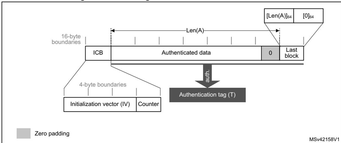
The diagram illustrates the message construction for GMAC. It shows a sequence of blocks: an Initialization Vector (IV) and Counter (ICB) followed by Authenticated data and a Last block. The ICB is split into a 16-byte boundary (Initialization vector (IV)) and a 4-byte boundary (Counter). The Authenticated data is split into 16-byte boundaries. The Last block contains zero padding and length fields: [Len(A)] 64 and [0] 64 . An arrow labeled 'auth.' points from the Authenticated data to an Authentication tag (T). A legend indicates that grey boxes represent zero padding. The identifier MSv42158V1 is present in the bottom right corner.
AES GMAC processing
Figure 213 describes the GMAC mode implementation in the AES peripheral. This mode is selected by writing 011 to the CHMOD[2:0] bitfield of the AES_CR register.
Figure 213. GMAC authentication mode
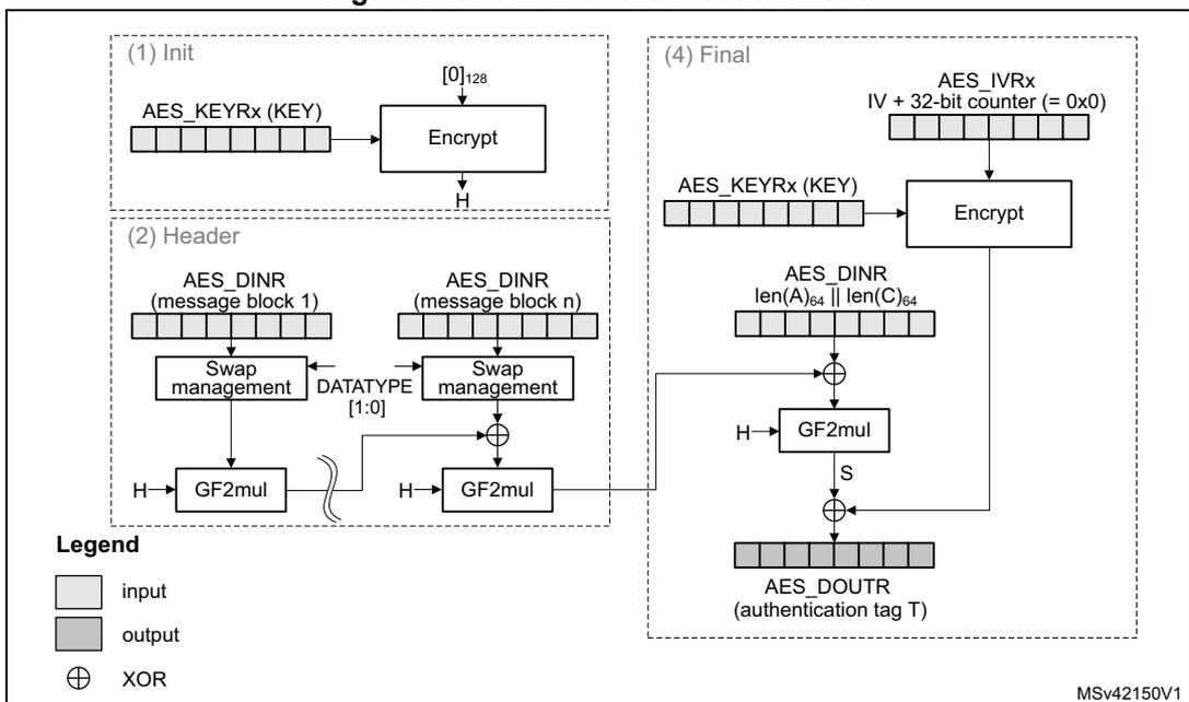
The flowchart details the GMAC authentication mode implementation in four stages: (1) Init, (2) Header, (3) Payload (omitted), and (4) Final.
(1) Init: AES_KEYRx (KEY) and [0]
128
are input to an Encrypt block, which outputs H.
(2) Header: AES_DINR (message block 1) and AES_DINR (message block n) are processed through Swap management blocks (controlled by DATATYPE [1:0]) and GF2mul blocks (taking H as input). The outputs are XORed together.
(4) Final: The XORed header data is input to a GF2mul block (taking H as input). The output S is XORed with the output of an Encrypt block (taking AES_KEYRx (KEY) and IV + 32-bit counter (= 0x0) as input). The final result is AES_DOUTR (authentication tag T).
A legend indicates: white boxes for input, grey boxes for output, and a circle with a cross for XOR. The identifier MSv42150V1 is present in the bottom right corner.
The GMAC algorithm corresponds to the GCM algorithm applied on a message only containing a header. As a consequence, all steps and settings are the same as with the GCM, except that the payload phase is omitted.
Suspend/resume operations in GMAC
In GMAC mode, the sequence described for the GCM applies except that only the header phase can be interrupted.
28.4.12 AES counter with CBC-MAC (CCM)
Overview
The AES counter with cipher block chaining-message authentication code (CCM) algorithm allows encryption and authentication of plaintext, generating the corresponding ciphertext and tag (also known as message authentication code). To ensure confidentiality, the CCM algorithm is based on AES in counter mode. It uses cipher block chaining technique to generate the message authentication code. This is commonly called CBC-MAC.
Note: NIST does not approve this CBC-MAC as an authentication mode outside the context of the CCM specification.
CCM chaining is specified in NIST Special Publication 800-38C, Recommendation for Block Cipher Modes of Operation - The CCM Mode for Authentication and Confidentiality . A typical message construction for CCM is given in Figure 214 .
Figure 214. Message construction in CCM mode
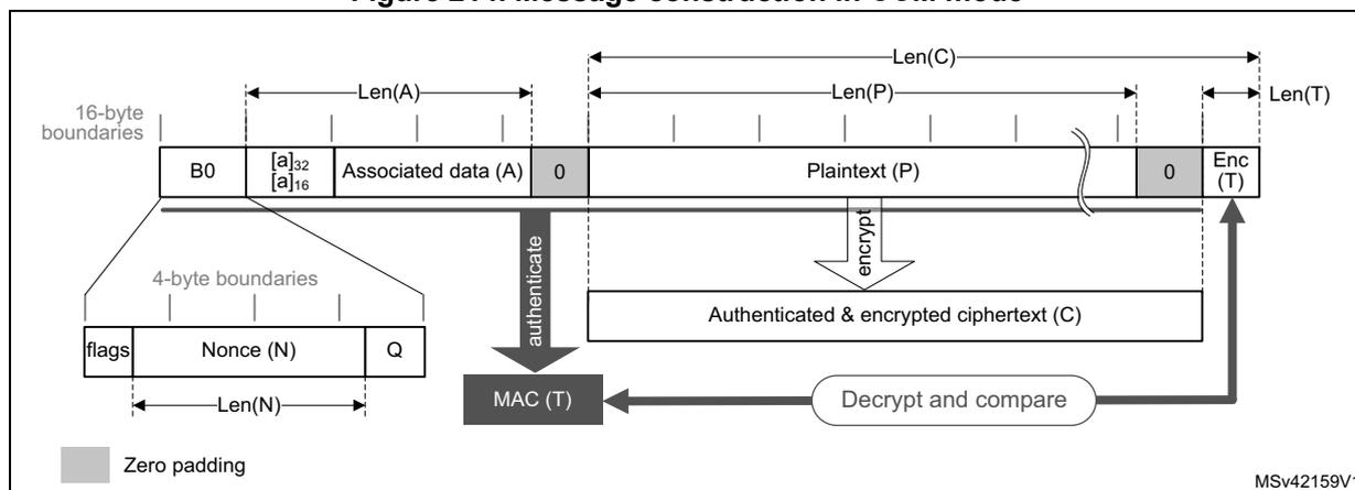
The structure of the message is:
- •
16-byte first authentication block (B0)
, composed of three distinct fields:
- – Q: a bit string representation of the octet length of P (Len(P))
- – Nonce (N): a single-use value (that is, a new nonce should be assigned to each new communication) of Len(N) size. The sum Len(N) + Len(P) must be equal to 15 bytes.
- – Flags: most significant octet containing four flags for control information, as specified by the standard. It contains two 3-bit strings to encode the values t (MAC length expressed in bytes) and Q (plaintext length such that \( \text{Len}(P) < 2^{8Q} \) bytes). The counter blocks range associated to Q is equal to \( 2^{8Q-4} \) , that is, if the maximum value of Q is 8, the counter blocks used in cipher shall be on 60 bits.
- •
16-byte blocks (B)
associated to the Associated Data (A).
This part of the message is only authenticated, not encrypted. This section has a known length Len(A) that can be a non-multiple of 16 bytes (see Figure 214 ). The
standard also states that, on MSB bits of the first message block (B1), the associated data length expressed in bytes (a) must be encoded as follows:
- – If \( 0 < a < 2^{16} - 2^8 \) , then it is encoded as \( [a]_{16} \) , that is, on two bytes.
- – If \( 2^{16} - 2^8 < a < 2^{32} \) , then it is encoded as 0xff || 0xfe || \( [a]_{32} \) , that is, on six bytes.
- – If \( 2^{32} < a < 2^{64} \) , then it is encoded as 0xff || 0xff || \( [a]_{64} \) , that is, on ten bytes.
- • 16-byte blocks (B) associated to the plaintext message P, which is both authenticated and encrypted as ciphertext C, with a known length Len(P). This length can be a non-multiple of 16 bytes (see Figure 214 ).
- • Encrypted MAC (T) of length Len(T) appended to the ciphertext C of overall length Len(C).
When a part of the message (A or P) has a length that is a non-multiple of 16-bytes, a special padding scheme is required.
Note: CCM chaining mode can also be used with associated data only (that is, no payload).
As an example, the C.1 section in NIST Special Publication 800-38C gives the following values (hexadecimal numbers):
N: 10111213 141516 (Len(N)= 56 bits or 7 bytes)
A: 00010203 04050607 (Len(A)= 64 bits or 8 bytes)
P:
20212223
(Len(P)= 32 bits or 4 bytes)
T: 6084341B (Len(T)= 32 bits or t = 4)
B0: 4F101112 13141516 00000000 00000004
B1: 0008
0001
02030405
06070000 00000000
B2:
20212223
00000000 00000000 00000000
CTR0: 0710111213 141516 00000000 00000000
CTR1: 0710111213 141516 00000000 00000001
Generation of formatted input data blocks B x (especially B0 and B1) must be managed by the application.
CCM processing
Figure 215 describes the CCM implementation within the AES peripheral (decryption example).
Figure 215. CCM mode authenticated decryption
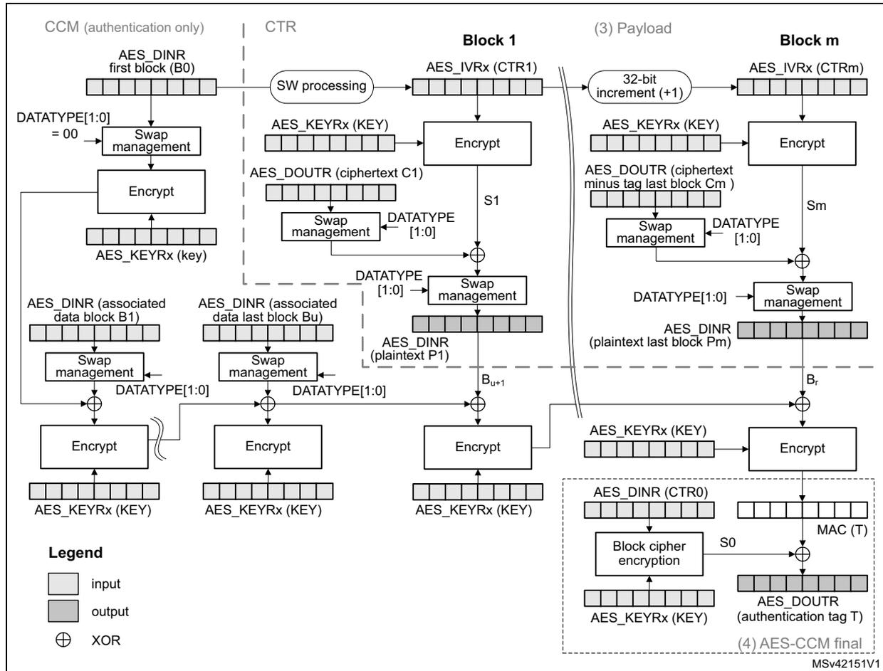
The data input to the generation-encryption process are a valid nonce, a valid payload string, and a valid associated data string, all properly formatted. The CBC chaining mechanism is applied to the formatted plaintext data to generate a MAC, with a known length. Counter mode encryption that requires a sufficiently long sequence of counter blocks as input, is applied to the payload string and separately to the MAC. The resulting ciphertext C is the output of the generation-encryption process on plaintext P.
AES_IVRx registers are used for processing each data block, AES automatically incrementing the CTR counter with a bit length defined by the first block B0. Table 183 shows how the application must load the B0 data.
Table 183. Initialization of AES_IVRx registers in CCM mode
| Register | AES_IVR3[31:0] | AES_IVR2[31:0] | AES_IVR1[31:0] | AES_IVR0[31:0] |
|---|---|---|---|---|
| Input data | B0[31:0] | B0[63:32] | B0[95:64] | B0[127:96] |
A CCM message is processed through two distinct processes - first, payload encryption or decryption , in which the AES peripheral is configured in CTR mode, then associated data and payload authentication , in which the AES peripheral first executes the CCM header phase, then the CCM final phase.
Payload encryption/decryption
This step is performed independently of the tag computation. It uses standard CTR chaining mode. Refer to Section 28.4.9: AES counter (CTR) mode for details. The construction of the CTR1 initialization vector (see Figure 215 ) to load into AES_IVRx registers is defined in NIST Special Publication 800-38C.
Note: This phase can be skipped if there is no payload data, that is, when \( Len(P) = 0 \) or \( Len(C) = Len(T) \) .
Remove \( LSB_{Len(T)}(C) \) encrypted tag information when decrypting ciphertext C.
Associated data and payload authentication
In order to compute the CCM authentication tag associated with the plaintext message, it is recommended to execute the following header phase sequence:
- 1. Ensure that the AES peripheral is disabled (the EN bit of the AES_CR must be 0).
- 2. Select CCM chaining mode, by setting to 100 the CHMOD[2:0] bitfield of the AES_CR register, and optionally, set the DATATYPE[1:0] bitfield.
- 3. Indicate the header phase, by setting to 01 the GCMPH[1:0] bitfield of the AES_CR register. Select encrypt mode by setting to 00 the MODE[1:0] bitfield of the AES_CR register.
- 4. Initialize the AES_KEYRx registers with a key, and initialize AES_IVRx registers with zero values.
- 5. Enable the AES peripheral by setting the EN bit of the AES_CR register.
- 6. Write the AES_DINR register with B0, as shown in Table 183 . B0 data must be swapped according to the DATATYPE[1:0] bitfield of the AES_CR register.
- 7. Wait until the end-of-computation flag CCF of the AES_SR register is set to 1.
- 8. Clear the CCF flag of the AES_SR register by setting the CCFC bit of the AES_CR register.
- 9. Process data block. If it is the last block of associated data or plaintext and data size in the block is inferior to 128 bits, pad the remainder of the block with zeros. Then append the data block into AES in one of ways described in Section 28.4.4: AES procedure to perform a cipher operation on page 828 .
- 10. Repeat the previous step to process all data blocks, starting from the first block of associated data and ending with the last block of plaintext payload data.
In final phase, the AES peripheral generates the CCM authentication tag and stores it in the AES_DOUTR register:
- 11. Indicate the final phase, by setting to 11 the GCMPH[1:0] bitfield of the AES_CR register. Keep as-is the encryption mode in the MODE[1:0] bitfield.
- 12. Write four times the last data input into the AES_DIN register. This input must be the 128-bit value CTR0, formatted from the original B0 packet (that is, 5 flag bits set to 0, and Q length bits set to 0).
- 13. Wait until the end-of-computation flag CCF of the AES_SR register is set.
- 14. Read four times the AES_DOUTR register: the output corresponds to the encrypted CCM authentication tag.
- 15. Clear the CCF flag of the AES_SR register by setting the CCFC bit of the AES_CR register.
- 16. Disable the AES peripheral, by clearing the EN bit of the AES_CR register.
- 17. For authenticated decryption, compare the generated encrypted tag with the encrypted tag padded in the ciphertext.
Note: In this final phase, data must be swapped according to the DATATYPE[1:0] bitfield of the AES_CR register.
When transiting from the header phase to the final phase, the AES peripheral must not be disabled, otherwise the result is wrong.
Application must mask the authentication tag output with tag length to obtain a valid tag.
Suspend/resume operations in CCM mode
To suspend the authentication of the associated data and payload (GCMPH[1:0]= 01), proceed as follows. Suspending the message during the encryption/decryption phase is described in Section 28.4.9: AES counter (CTR) mode on page 840 .
- 1. If DMA is used, stop the AES DMA transfers to the IN FIFO by clearing the DMAINEN bit of the AES_CR register. If DMA is not used, make sure that the current computation is completed, which is indicated by the CCF flag of the AES_SR register set to 1.
- 2. Clear the CCF flag of the AES_SR register, by setting to 1 the CCFC bit of the AES_CR register.
- 3. Save the AES_SUSPxR registers (where x is from 0 to 7) in the memory.
- 4. Save the AES_IVRx registers, as during the data processing they changed from their initial values.
- 5. Disable the AES peripheral, by clearing the bit EN of the AES_CR register.
- 6. Save the current AES configuration in the memory, excluding the initialization vector registers AES_IVRx. Key registers do not need to be saved as the original key value is known by the application.
- 7. If DMA is used, save the DMA controller status (pointers for IN data transfers, number of remaining bytes, and so on).
To resume the authentication of the associated data and payload (GCM PH [1:0]= 01 or 11), proceed as follows:
- 1. If DMA is used, configure the DMA controller in order to complete the rest of the FIFO IN transfers.
- 2. Ensure that AES processor is disabled (the EN bit of the AES_CR register must be 0).
- 3. Write the suspend register values, previously saved in the memory, back into their corresponding AES_SUSPxR registers (where x is from 0 to 7).
- 4. Write the initialization vector register values, previously saved in the memory, back into their corresponding AES_IVRx registers.
- 5. Restore the initial setting values in the AES_CR and AES_KEYRx registers.
- 6. Enable the AES peripheral by setting the EN bit of the AES_CR register.
- 7. If DMA is used, enable AES DMA requests by setting the DMAINEN bit of the AES_CR register.
Note: In CCM mode the MODE[1:0] bitfield settings 01 and 11 (key derivation) are forbidden.
28.4.13 .AES data registers and data swapping
Data input and output
A 128-bit data block is entered into the AES peripheral with four successive 32-bit word writes into the AES_DINR register (bitfield DIN[127:0]), the most significant word (bits [127:96]) first, the least significant word (bits [31:0]) last.
A 128-bit data block is retrieved from the AES peripheral with four successive 32-bit word reads from the AES_DOUTR register (bitfield DOUT[127:0]), the most significant word (bits [127:96]) first, the least significant word (bits [31:0]) last.
The 32-bit data word for AES_DINR register or from AES_DOUTR register is organized in big endian order, that is:
- • the most significant byte of a word to write into AES_DINR must be put on the lowest address out of the four adjacent memory locations keeping the word to write, or
- • the most significant byte of a word read from AES_DOUTR goes to the lowest address out of the four adjacent memory locations receiving the word
For using DMA for input data block write into AES, the four words of the input block must be stored in the memory consecutively and in big-endian order, that is, the most significant word on the lowest address. See Section 28.4.16: AES DMA interface .
Data swapping
The AES peripheral can be configured to perform a bit-, a byte-, a half-word-, or no swapping on the input data word in the AES_DINR register, before loading it to the AES processing core, and on the data output from the AES processing core, before sending it to the AES_DOUTR register. The choice depends on the type of data. For example, a byte swapping is used for an ASCII text stream.
The data swap type is selected through the DATATYPE[1:0] bitfield of the AES_CR register. The selection applies both to the input and the output of the AES core.
For different data swap types, Figure 216 shows the construction of AES processing core input buffer data P127..0, from the input data entered through the AES_DINR register, or the construction of the output data available through the AES_DOUTR register, from the AES processing core output buffer data P127..0.
Figure 216. 128-bit block construction with respect to data swap
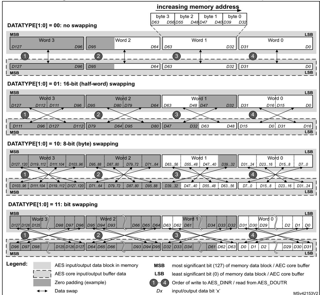
increasing memory address →
DATATYPE[1:0] = 00: no swapping
byte 3 (D63..D56), byte 2 (D55..D48), byte 1 (D47..D40), byte 0 (D39..D32)
MSB Word 3 (D127..D96) Word 2 (D95..D64) Word 1 (D63..D32) Word 0 (D31..D0) LSB
① ② ③ ④
D127 D96 D95 D64 D63 D32 D31 D0
MSB LSB
DATATYPE[1:0] = 01: 16-bit (half-word) swapping
MSB Word 3 (D127..D112, D111..D96) Word 2 (D95..D80, D79..D64) Word 1 (D63..D48, D47..D32) Word 0 (D31..D16, D15..D0) LSB
① ② ③ ④
D111 D96 D127 D112 D79 D64 D95 D80 D47 D32 D63 D48 D15 D0 D31 D16
MSB LSB
DATATYPE[1:0] = 10: 8-bit (byte) swapping
MSB Word 3 (D127..120, D119..112, D111..104, D103..96) Word 2 (D95..88, D87..80, D79..72, D71..64) Word 1 (D63..56, D55..48, D47..40, D39..32) Word 0 (D31..24, D23..16, D15..8, D7..0) LSB
① ② ③ ④
D103..96 D111..104 D119..112 D127..120 D71..64 D79..72 D87..80 D95..88 D39..32 D47..40 D55..48 D63..56 D7..0 D15..8 D23..16 D31..24
MSB LSB
DATATYPE[1:0] = 11: bit swapping
MSB Word 3 (D127, D126, D125, D98, D97, D96) Word 2 (D95, D94, D93, D66, D65, D64) Word 1 (D63, D62, D61, D34, D33, D32) Word 0 (D31, D30, D29, D2, D1, D0) LSB
① ② ③ ④
D96 D97 D98 D125 D126 D127 D64 D65 D66 D93 D94 D95 D32 D33 D34 D61 D62 D63 D0 D1 D2 D29 D30 D31
MSB LSB
Legend:
- AES input/output data block in memory
- AES core input/output buffer data
- Zero padding (example)
- Data swap
- MSB most significant bit (127) of memory data block / AEC core buffer
- LSB least significant bit (0) of memory data block / AEC core buffer
- ①..④ Order of write to AES_DINR / read from AES_DOUTR
- D x input/output data bit 'x'
Note: The data in AES key registers (AES_KEYRx) and initialization registers (AES_IVRx) are not sensitive to the swap mode selection.
Data padding
Figure 216 also gives an example of memory data block padding with zeros such that the zeroed bits after the data swap form a contiguous zone at the MSB end of the AES core input buffer. The example shows the padding of an input data block containing:
- • 48 message bits, with DATATYPE[1:0] = 01
- • 56 message bits, with DATATYPE[1:0] = 10
- • 34 message bits, with DATATYPE[1:0] = 11
28.4.14 AES key registers
The AES_KEYRx registers store the encryption or decryption key bitfield KEY[127:0] or KEY[255:0]. The data to write to or to read from each register is organized in the memory in little-endian order, that is, with most significant byte on the highest address.
The key is spread over the eight registers as shown in Table 184 .
Table 184. Key endianness in AES_KEYRx registers (128- or 256-bit key length)
| AES_KEYR7 [31:0] | AES_KEYR6 [31:0] | AES_KEYR5 [31:0] | AES_KEYR4 [31:0] | AES_KEYR3 [31:0] | AES_KEYR2 [31:0] | AES_KEYR1 [31:0] | AES_KEYR0 [31:0] |
|---|---|---|---|---|---|---|---|
| - | - | - | - | KEY[127:96] | KEY[95:64] | KEY[63:32] | KEY[31:0] |
| KEY[255:224] | KEY[223:192] | KEY[191:160] | KEY[159:128] | KEY[127:96] | KEY[95:64] | KEY[63:32] | KEY[31:0] |
The key for encryption or decryption may be written into these registers when the AES peripheral is disabled.
The key registers are not affected by the data swapping controlled by DATATYPE[1:0] bitfield of the AES_CR register.
28.4.15 AES initialization vector registers
The four AES_IVRx registers keep the initialization vector input bitfield IVI[127:0]. The data to write to or to read from each register is organized in the memory in little-endian order, that is, with most significant byte on the highest address. The registers are also ordered from lowest address (AES_IVR0) to highest address (AES_IVR3).
The signification of data in the bitfield depends on the chaining mode selected. When used, the bitfield is updated upon each computation cycle of the AES core.
Write operations to the AES_IVRx registers when the AES peripheral is enabled have no effect to the register contents. For modifying the contents of the AES_IVRx registers, the EN bit of the AES_CR register must first be cleared.
Reading the AES_IVRx registers returns the latest counter value (useful for managing suspend mode).
The AES_IVRx registers are not affected by the data swapping feature controlled by the DATATYPE[1:0] bitfield of the CRYP_CR register.
28.4.16 AES DMA interface
The AES peripheral provides an interface to connect to the DMA (direct memory access) controller. The DMA operation is controlled through the AES_CR register.
Data input using DMA
Setting the DMAINEN bit of the AES_CR register enables DMA writing into AES. The AES peripheral then initiates a DMA request during the input phase each time it requires a word to be written to the AES_DINR register. It asserts four DMA requests to transfer one 128-bit (four-word) input data block from memory, as shown in Figure 217 .
See Table 185 for recommended DMA configuration.
Table 185. DMA channel configuration for memory-to-AES data transfer
| DMA channel control register field | Recommended configuration |
|---|---|
| Transfer size | Message length: a multiple of 128 bits. According to the algorithm and the mode selected, special padding/ciphertext stealing might be required. Refer to Section 28.4.6: AES ciphertext stealing and data padding on page 833 for details. |
| Source burst size (memory) | Single |
| Destination burst size (peripheral) | Single |
| DMA FIFO size | AES_FIFO_size = 4 bytes. |
| Source transfer width (memory) | 32-bit words |
| Destination transfer width (peripheral) | 32-bit words |
| Source address increment (memory) | Yes, after each 32-bit transfer |
| Destination address increment (peripheral) | Fixed address of AES_DINR (no increment) |
Figure 217. DMA transfer of a 128-bit data block during input phase
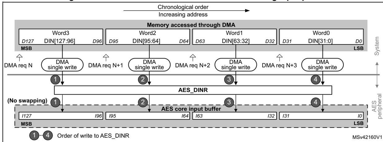
The diagram illustrates the DMA transfer of a 128-bit data block during the input phase. At the top, a horizontal arrow indicates 'Chronological order' and 'Increasing address'. Below this, a section titled 'Memory accessed through DMA' shows four words: Word3 (D127 to D96), Word2 (D95 to D64), Word1 (D63 to D32), and Word0 (D31 to D0). Each word is associated with a 'DMA single write' operation, triggered by DMA requests N, N+1, N+2, and N+3. Arrows show the data being written from these DMA operations into the 'AES_DINR' register. From the AES_DINR register, the data is then transferred into the 'AES core input buffer'. The buffer is shown with bit positions: 1127, 196, 195, 164, 163, 132, 131, and 10. A dashed line indicates 'No swapping'. At the bottom, a sequence of four numbered circles (1 to 4) indicates the 'Order of write to AES_DINR'. The diagram is labeled 'MSV42160V1' in the bottom right corner.
Data output using DMA
Setting the DMAOUTEN bit of the AES_CR register enables DMA reading from AES. The AES peripheral then initiates a DMA request during the Output phase each time it requires a word to be read from the AES_DOUTR register. It asserts four DMA requests to transfer one 128-bit (four-word) output data block to memory, as shown in Figure 218 .
See Table 186 for recommended DMA configuration.
Table 186. DMA channel configuration for AES-to-memory data transfer
| DMA channel control register field | Recommended configuration |
|---|---|
| Transfer size | It is the message length multiple of AES block size (4 words). According to the case extra bytes will have to be discarded. |
| Source burst size (peripheral) | Single |
| Destination burst size (memory) | Single |
| DMA FIFO size | AES_FIFO_size = 4 bytes |
| Source transfer width (peripheral) | 32-bit words |
| Destination transfer width (memory) | 32-bit words |
| Source address increment (peripheral) | Fixed address of AES_DINR (no increment) |
| Destination address increment (memory) | Yes, after each 32-bit transfer |
Figure 218. DMA transfer of a 128-bit data block during output phase
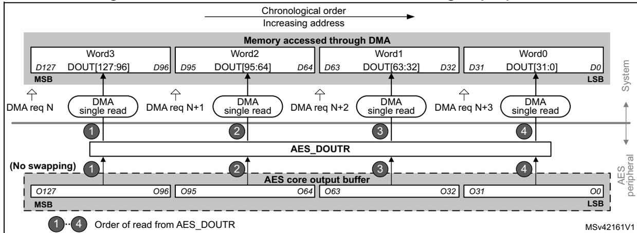
The diagram illustrates the data flow during the output phase of a 128-bit data block. At the top, 'Memory accessed through DMA' shows four words: Word3 (D127:DOUT[127:96]), Word2 (D95:DOUT[95:64]), Word1 (D63:DOUT[63:32]), and Word0 (D31:DOUT[31:0]). Below this, four 'DMA single read' operations are shown, triggered by DMA requests N, N+1, N+2, and N+3. These reads transfer data from the 'AES_DOUTR' register to the memory. The 'AES core output buffer' at the bottom shows the internal data organization (O127 to O0) which is read in the same order (1 to 4) as it is transferred to memory. A note indicates '(No swapping)'. The diagram is labeled 'System' on the right and 'AES peripheral' on the right. Reference MSV42161V1 is at the bottom right.
DMA operation in different operating modes
DMA operations are usable when Mode 1 (encryption) or Mode 3 (decryption) are selected via the MODE[1:0] bitfield of the register AES_CR. As in Mode 2 (key derivation) the AES_KEYRx registers must be written by software, enabling the DMA transfer through the DMAINEN and DMAOUTEN bits of the AES_CR register have no effect in that mode.
DMA single requests are generated by AES until it is disabled. So, after the data output phase at the end of processing of a 128-bit data block, AES switches automatically to a new data input phase for the next data block, if any.
When the data transferring between AES and memory is managed by DMA, the CCF flag is not relevant and can be ignored (left set) by software. It must only be cleared when
transiting back to data transferring managed by software. See Suspend/resume operations in ECB/CBC modes in Section 28.4.8: AES basic chaining modes (ECB, CBC) as example.
28.4.17 AES error management
The read error flag (RDERR) and write error flag (WRERR) of the AES_SR register are set when an unexpected read or write operation, respectively, is detected. An interrupt can be generated if the error interrupt enable (ERRIE) bit of the AES_CR register is set. For more details, refer to Section 28.5: AES interrupts .
Note: AES is not disabled after an error detection and continues processing.
AES can be re-initialized at any moment by clearing then setting the EN bit of the AES_CR register.
Read error flag (RDERR)
When an unexpected read operation is detected during the computation phase or during the input phase, the AES read error flag (RDERR) is set in the AES_SR register. An interrupt is generated if the ERRIE bit of the AES_CR register is set.
The RDERR flag is cleared by setting the corresponding ERRC bit of the AES_CR register.
Write error flag (WDERR)
When an unexpected write operation is detected during the computation phase or during the output phase, the AES write error flag (WRERR) is set in the AES_SR register. An interrupt is generated if the ERRIE bit of the AES_CR register is set.
The WDERR flag is cleared by setting the corresponding ERRC bit of the AES_CR register.
28.5 AES interrupts
There are three individual maskable interrupt sources generated by the AES peripheral, to signal the following events:
- • computation completed
- • read error, see Section 28.4.17
- • write error, see Section 28.4.17
These three sources are combined into a common interrupt signal aes_it that connects to NVIC (nested vectored interrupt controller).
Figure 219. AES interrupt signal generation
The diagram illustrates the logic for generating the AES interrupt signal (aes_it). It shows three pairs of inputs, each consisting of a flag from the AES_SR register and a corresponding enable bit from the AES_CR register. These pairs are: (CCF, CCFIE), (WRERR, ERRIE), and (RDERR, ERRIE). Each pair is connected to an AND gate. The outputs of these three AND gates are then connected to a single OR gate. The output of the OR gate is the aes_it signal, which is directed to the NVIC. A label on the left side of the diagram groups the inputs as 'Flags in AES_SR register' and 'Bits of AES_CR register'. A small code 'MSV42162V1' is visible in the bottom right corner of the diagram box.
Each AES interrupt source can individually be enabled/disabled, by setting/clearing the corresponding enable bit of the AES_CR register. See Figure 219 .
The status of the individual maskable interrupt sources can be read from the AES_SR register.
Table 187 gives a summary of the interrupt sources, their event flags and enable bits.
Table 187. AES interrupt requests
| AES interrupt event | Event flag | Enable bit |
|---|---|---|
| computation completed flag | CCF | CCFIE |
| read error flag | RDERR | ERRIE |
| write error flag | WRERR | ERRIE |
28.6 AES processing latency
The tables below summarize the latency to process a 128-bit block for each mode of operation.
Table 188. Processing latency (in clock cycle) for ECB, CBC and CTR
| Key size | Mode of operation | Algorithm | Input phase | Computation phase | Output phase | Total |
|---|---|---|---|---|---|---|
| 128-bit | Mode 1: Encryption | ECB, CBC, CTR | 8 | 202 | 4 | 214 |
| Mode 2: Key derivation | - | - | 80 | - | 80 | |
| Mode 3: Decryption | ECB, CBC, CTR | 8 | 202 | 4 | 214 | |
| Mode 4: Key derivation then decryption | ECB, CBC | 8 | 276 | 4 | 288 | |
| 256-bit | Mode 1: Encryption | ECB, CBC, CTR | 8 | 286 | 4 | 298 |
| Mode 2: Key derivation | - | - | 109 | - | 109 | |
| Mode 3: Decryption | ECB, CBC, CTR | 8 | 286 | 4 | 298 | |
| Mode 4: Key derivation then decryption | ECB, CBC | 8 | 380 | 4 | 392 |
Table 189. Processing latency for GCM and CCM (in clock cycle)
| Key size | Mode of operation | Algorithm | Init Phase | Header phase | Payload phase | Tag phase |
|---|---|---|---|---|---|---|
| 128-bit | Mode 1: Encryption/ Mode 3: Decryption | GCM | 215 | 67 | 202 | 202 |
| - | CCM authentication | - | 206 | - | 202 | |
| 256-bit | Mode 1: Encryption/ Mode 3: Decryption | GCM | 299 | 67 | 286 | 286 |
| - | CCM authentication | - | 290 | - | 286 |
Note: Data insertion can include wait states forced by AES on the AHB bus (maximum 3 cycles, typical 1 cycle). This applies to all header/payload/tag phases.
28.7 AES registers
28.7.1 AES control register (AES_CR)
Address offset: 0x00
Reset value: 0x0000 0000
| 31 | 30 | 29 | 28 | 27 | 26 | 25 | 24 | 23 | 22 | 21 | 20 | 19 | 18 | 17 | 16 |
|---|---|---|---|---|---|---|---|---|---|---|---|---|---|---|---|
| Res. | Res. | Res. | Res. | Res. | Res. | Res. | Res. | Res. | Res. | Res. | Res. | Res. | KEYSIZE | Res. | CHMOD[2] |
| rw | rw | ||||||||||||||
| 15 | 14 | 13 | 12 | 11 | 10 | 9 | 8 | 7 | 6 | 5 | 4 | 3 | 2 | 1 | 0 |
| Res. | GCMPH[1:0] | DMAOUTEN | DMAINEN | ERRIE | CCFIE | ERRC | CCFC | CHMOD[1:0] | MODE[1:0] | DATATYPE[1:0] | EN | ||||
| rw | rw | rw | rw | rw | rw | rw | rw | rw | rw | rw | rw | rw | rw | rw | |
Bits 31:19 Reserved, must be kept at zero
Bit 18 KEYSIZE : Key size selection
This bitfield defines the length of the key used in the AES cryptographic core, in bits:
0: 128
1: 256
The bit value change is allowed only when AES is disabled, so as to avoid an unpredictable behavior.
Bit 17 Reserved, must be kept at zero
Bit 16 CHMOD[2] : Chaining mode selection, bit [2]
Refer to the bits [5:6] of the register for the description of the CHMOD[2:0] bitfield
Bit 15 Reserved, must be kept at zero
Bits 14:13 GCMPH[1:0] : GCM or CCM phase selection
This bitfield selects the phase of GCM, GMAC or CCM algorithm:
00: Init phase
01: Header phase
10: Payload phase
11: Final phase
The bitfield has no effect if other than GCM, GMAC or CCM algorithms are selected (through the ALGOMODE bitfield).
Bit 12 DMAOUTEN: DMA output enableThis bit enables/disables data transferring with DMA, in the output phase:
0: Disable
1: Enable
When the bit is set, DMA requests are automatically generated by AES during the output data phase. This feature is only effective when Mode 1 or Mode 3 is selected through the MODE[1:0] bitfield. It is not effective for Mode 2 (key derivation).
Usage of DMA with Mode 4 (single decryption) is not recommended.
Bit 11 DMAINEN: DMA input enableThis bit enables/disables data transferring with DMA, in the input phase:
0: Disable
1: Enable
When the bit is set, DMA requests are automatically generated by AES during the input data phase. This feature is only effective when Mode 1 or Mode 3 is selected through the MODE[1:0] bitfield. It is not effective for Mode 2 (key derivation).
Usage of DMA with Mode 4 (single decryption) is not recommended.
Bit 10 ERRIE: Error interrupt enableThis bit enables or disables (masks) the AES interrupt generation when RDERR and/or WRERR is set:
0: Disable (mask)
1: Enable
Bit 9 CCFIE: CCF interrupt enableThis bit enables or disables (masks) the AES interrupt generation when CCF (computation complete flag) is set:
0: Disable (mask)
1: Enable
Bit 8 ERRRC: Error flag clearUpon written to 1, this bit clears the RDERR and WRERR error flags in the AES_SR register:
0: No effect
1: Clear RDERR and WRERR flags
Reading the flag always returns zero.
Bit 7 CCFC: Computation complete flag clearUpon written to 1, this bit clears the computation complete flag (CCF) in the AES_SR register:
0: No effect
1: Clear CCF
Reading the flag always returns zero.
Bits 6:5 CHMOD[1:0] : Chaining mode selection, bits [1:0]
These bits, together with the bit CHMOD[2] (see bit 16 of this register), form CHMOD[2:0] bitfield that selects the AES chaining mode:
- 000: Electronic codebook (ECB)
- 001: Cipher-Block Chaining (CBC)
- 010: Counter Mode (CTR)
- 011: Galois Counter Mode (GCM) and Galois Message Authentication Code (GMAC)
- 100: Counter with CBC-MAC (CCM)
- >100: Reserved
The bitfield value change is allowed only when AES is disabled, so as to avoid an unpredictable behavior.
Bits 4:3 MODE[1:0] : AES operating mode
This bitfield selects the AES operating mode:
- 00: Mode 1: encryption
- 01: Mode 2: key derivation (or key preparation for ECB/CBC decryption)
- 10: Mode 3: decryption
- 11: Mode 4: key derivation then single decryption
The bitfield value change is allowed only when AES is disabled, so as to avoid an unpredictable behavior. Any attempt to selecting Mode 4 while either ECB or CBC chaining mode is not selected, defaults to effective selection of Mode 3. It is not possible to select a Mode 3 following a Mode 4.
Bits 2:1 DATATYPE[1:0] : Data type selection
This bitfield defines the format of data written in the AES_DINR register or read from the AES_DOUTR register, through selecting the mode of data swapping:
- 00: None
- 01: Half-word (16-bit)
- 10: Byte (8-bit)
- 11: Bit
For more details, refer to Section 28.4.13: .AES data registers and data swapping .
The bitfield value change is allowed only when AES is disabled, so as to avoid an unpredictable behavior.
Bit 0 EN : AES enable
This bit enables/disables the AES peripheral:
- 0: Disable
- 1: Enable
At any moment, clearing then setting the bit re-initializes the AES peripheral.
This bit is automatically cleared by hardware when the key preparation process ends (Mode 2).
28.7.2 AES status register (AES_SR)
Address offset: 0x04
Reset value: 0x0000 0000
| 31 | 30 | 29 | 28 | 27 | 26 | 25 | 24 | 23 | 22 | 21 | 20 | 19 | 18 | 17 | 16 |
| Res. | Res. | Res. | Res. | Res. | Res. | Res. | Res. | Res. | Res. | Res. | Res. | Res. | Res. | Res. | Res. |
| r | r | r | r | r | r | r | r | r | r | r | r | r | r | r | r |
| 15 | 14 | 13 | 12 | 11 | 10 | 9 | 8 | 7 | 6 | 5 | 4 | 3 | 2 | 1 | 0 |
| Res. | Res. | Res. | Res. | Res. | Res. | Res. | Res. | Res. | Res. | Res. | Res. | BUSY | WRERR | RDERR | CCF |
| r | r | r | r | r | r | r | r | r | r | r | r | r | r | r | r |
Bits 31:4 Reserved, must be kept at zero
Bit 3 BUSY : Busy
This flag indicates whether AES is idle or busy during GCM payload encryption phase:
0: Idle
1: Busy
The flag is controlled by hardware. When the flag indicates “idle”, the current message processing may be suspended to process a higher-priority message.
This flag is effective only in GCM payload encryption phase. In other chaining modes, or in GCM phases other than payload encryption, the flag must be ignored.
Bit 2 WRERR : Write error
This flag indicates the detection of an unexpected write operation to the AES_DINR register (during computation or data output phase):
0: Not detected
1: Detected
The flag is set by hardware. It is cleared by software upon setting the ERRRC bit of the AES_CR register.
Upon the flag setting, an interrupt is generated if enabled through the ERRRIE bit of the AES_CR register.
The flag setting has no impact on the AES operation.
The flag is not effective when key derivation mode, or GCM/CCM Init phase is selected.
Bit 1 RDERR : Read error flag
This flag indicates the detection of an unexpected read operation from the AES_DOUTR register (during computation or data input phase):
0: Not detected
1: Detected
The flag is set by hardware. It is cleared by software upon setting the ERRRC bit of the AES_CR register.
Upon the flag setting, an interrupt is generated if enabled through the ERRRIE bit of the AES_CR register.
The flag setting has no impact on the AES operation.
The flag is not effective when key derivation mode, nor GCM/CCM init/header phase is selected.
Bit 0 CCF : Computation completed flag
This flag indicates whether the computation is completed:
0: Not completed
1: Completed
The flag is set by hardware upon the completion of the computation. It is cleared by software, upon setting the CCFC bit of the AES_CR register.
Upon the flag setting, an interrupt is generated if enabled through the CCFIE bit of the AES_CR register.
The flag is significant only when the DMAOUTEN bit is 0. It may stay high when DMA_EN is 1.
28.7.3 AES data input register (AES_DINR)
Address offset: 0x08
Reset value: 0x0000 0000
Only 32-bit access type is supported.
| 31 | 30 | 29 | 28 | 27 | 26 | 25 | 24 | 23 | 22 | 21 | 20 | 19 | 18 | 17 | 16 |
|---|---|---|---|---|---|---|---|---|---|---|---|---|---|---|---|
| DIN[x+31:x+16] | |||||||||||||||
| rw | rw | rw | rw | rw | rw | rw | rw | rw | rw | rw | rw | rw | rw | rw | rw |
| 15 | 14 | 13 | 12 | 11 | 10 | 9 | 8 | 7 | 6 | 5 | 4 | 3 | 2 | 1 | 0 |
| DIN[x+15:x] | |||||||||||||||
| rw | rw | rw | rw | rw | rw | rw | rw | rw | rw | rw | rw | rw | rw | rw | rw |
Bits 31:0 DIN[x+31:x] : One of four 32-bit words of a 128-bit input data block being written into the peripheral. This bitfield feeds a 32-bit input buffer. A 4-fold sequential write to this bitfield during the input phase virtually writes a complete 128-bit block of input data to the AES peripheral. Upon each write, the data from the input buffer are handled by the data swap block according to the DATATYPE[1:0] bitfield, then written into the AES core 128-bit input buffer. The substitution for “x”, from the first to the fourth write operation, is: 96, 64, 32, and 0. In other words, data from the first to the fourth write operation are: DIN[127:96], DIN[95:64], DIN[63:32], and DIN[31:0]. The data signification of the input data block depends on the AES operating mode:
- - Mode 1 (encryption): plaintext
- - Mode 2 (key derivation): the bitfield is not used (AES_KEYRx registers used for input)
- - Mode 3 (decryption) and Mode 4 (key derivation then single decryption): ciphertext
The data swap operation is described in Section 28.4.13: .AES data registers and data swapping on page 854 .
28.7.4 AES data output register (AES_DOUTr)
Address offset: 0x0C
Reset value: 0x0000 0000
Only 32-bit access type is supported.
| 31 | 30 | 29 | 28 | 27 | 26 | 25 | 24 | 23 | 22 | 21 | 20 | 19 | 18 | 17 | 16 |
|---|---|---|---|---|---|---|---|---|---|---|---|---|---|---|---|
| DOUT[x+31:x+16] | |||||||||||||||
| r | r | r | r | r | r | r | r | r | r | r | r | r | r | r | r |
| 15 | 14 | 13 | 12 | 11 | 10 | 9 | 8 | 7 | 6 | 5 | 4 | 3 | 2 | 1 | 0 |
| DOUT[x+15:0] | |||||||||||||||
| r | r | r | r | r | r | r | r | r | r | r | r | r | r | r | r |
Bits 31:0 DOUT[x+31:x] : One of four 32-bit words of a 128-bit output data block being read from the peripheral. This bitfield fetches a 32-bit output buffer. A 4-fold sequential read of this bitfield, upon the computation completion (CCF set), virtually reads a complete 128-bit block of output data from the AES peripheral. Before reaching the output buffer, the data produced by the AES core are handled by the data swap block according to the DATATYPE[1:0] bitfield. The substitution for DOUT[x+31:x], from the first to the fourth read operation, is: 96, 64, 32, and 0. In other words, data from the first to the fourth read operation are: DOUT[127:96], DOUT[95:64], DOUT[63:32], and DOUT[31:0]. The data signification of the output data block depends on the AES operating mode:
- - Mode 1 (encryption): ciphertext
- - Mode 2 (key derivation): the bitfield is not used (AES_KEYRx registers used for output).
- - Mode 3 (decryption) and Mode 4 (key derivation then single decryption): plaintext
The data swap operation is described in Section 28.4.13: .AES data registers and data swapping on page 854 .
28.7.5 AES key register 0 (AES_KEYR0)
Address offset: 0x10
Reset value: 0x0000 0000
| 31 | 30 | 29 | 28 | 27 | 26 | 25 | 24 | 23 | 22 | 21 | 20 | 19 | 18 | 17 | 16 |
| KEY[31:16] | |||||||||||||||
| rw | rw | rw | rw | rw | rw | rw | rw | rw | rw | rw | rw | rw | rw | rw | rw |
| 15 | 14 | 13 | 12 | 11 | 10 | 9 | 8 | 7 | 6 | 5 | 4 | 3 | 2 | 1 | 0 |
| KEY[15:0] | |||||||||||||||
| rw | rw | rw | rw | rw | rw | rw | rw | rw | rw | rw | rw | rw | rw | rw | rw |
Bits 31:0 KEY[31:0] : Cryptographic key, bits [31:0]
This bitfield contains the bits [31:0] of the AES encryption or decryption key, depending on the operating mode:
- - In Mode 1 (encryption), Mode 2 (key derivation) and Mode 4 (key derivation then single decryption): the value to write into the bitfield is the encryption key.
- - In Mode 3 (decryption): the value to write into the bitfield is the encryption key to be derived before being used for decryption. After writing the encryption key into the bitfield, its reading before enabling AES returns the same value. Its reading after enabling AES and after the CCF flag is set returns the decryption key derived from the encryption key.
Note: In mode 4 (key derivation then decryption) the bitfield always contains the encryption key.
The AES_KEYRx registers may be written only when the AES peripheral is disabled.
Refer to Section 28.4.14: AES key registers on page 856 for more details.
28.7.6 AES key register 1 (AES_KEYR1)
Address offset: 0x14
Reset value: 0x0000 0000

| 31 | 30 | 29 | 28 | 27 | 26 | 25 | 24 | 23 | 22 | 21 | 20 | 19 | 18 | 17 | 16 |
| KEY[63:48] | |||||||||||||||
| rw | rw | rw | rw | rw | rw | rw | rw | rw | rw | rw | rw | rw | rw | rw | rw |
| 15 | 14 | 13 | 12 | 11 | 10 | 9 | 8 | 7 | 6 | 5 | 4 | 3 | 2 | 1 | 0 |
| KEY[47:32] | |||||||||||||||
| rw | rw | rw | rw | rw | rw | rw | rw | rw | rw | rw | rw | rw | rw | rw | rw |
Bits 31:0 KEY[63:32] : Cryptographic key, bits [63:32]
Refer to the AES_KEYR0 register for description of the KEY[255:0] bitfield.
28.7.7 AES key register 2 (AES_KEYR2)
Address offset: 0x18
Reset value: 0x0000 0000
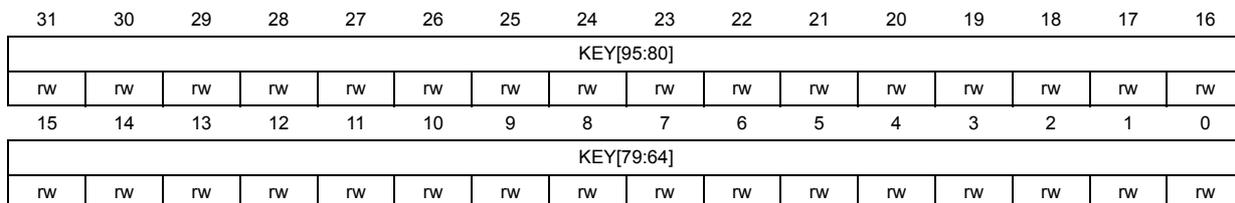
| 31 | 30 | 29 | 28 | 27 | 26 | 25 | 24 | 23 | 22 | 21 | 20 | 19 | 18 | 17 | 16 |
| KEY[95:80] | |||||||||||||||
| rw | rw | rw | rw | rw | rw | rw | rw | rw | rw | rw | rw | rw | rw | rw | rw |
| 15 | 14 | 13 | 12 | 11 | 10 | 9 | 8 | 7 | 6 | 5 | 4 | 3 | 2 | 1 | 0 |
| KEY[79:64] | |||||||||||||||
| rw | rw | rw | rw | rw | rw | rw | rw | rw | rw | rw | rw | rw | rw | rw | rw |
Bits 31:0
KEY[95:64]
: Cryptographic key, bits [95:64]
Refer to the AES_KEYR0 register for description of the KEY[255:0] bitfield.
28.7.8 AES key register 3 (AES_KEYR3)
Address offset: 0x1C
Reset value: 0x0000 0000
| 31 | 30 | 29 | 28 | 27 | 26 | 25 | 24 | 23 | 22 | 21 | 20 | 19 | 18 | 17 | 16 |
| KEY[127:112] | |||||||||||||||
| rw | rw | rw | rw | rw | rw | rw | rw | rw | rw | rw | rw | rw | rw | rw | rw |
| 15 | 14 | 13 | 12 | 11 | 10 | 9 | 8 | 7 | 6 | 5 | 4 | 3 | 2 | 1 | 0 |
| KEY[111:96] | |||||||||||||||
| rw | rw | rw | rw | rw | rw | rw | rw | rw | rw | rw | rw | rw | rw | rw | rw |
Bits 31:0
KEY[127:96]
: Cryptographic key, bits [127:96]
Refer to the AES_KEYR0 register for description of the KEY[255:0] bitfield.
28.7.9 AES initialization vector register 0 (AES_IVR0)
Address offset: 0x20
Reset value: 0x0000 0000
| 31 | 30 | 29 | 28 | 27 | 26 | 25 | 24 | 23 | 22 | 21 | 20 | 19 | 18 | 17 | 16 |
| IVI[31:16] | |||||||||||||||
| rw | rw | rw | rw | rw | rw | rw | rw | rw | rw | rw | rw | rw | rw | rw | rw |
| 15 | 14 | 13 | 12 | 11 | 10 | 9 | 8 | 7 | 6 | 5 | 4 | 3 | 2 | 1 | 0 |
| IVI[15:0] | |||||||||||||||
| rw | rw | rw | rw | rw | rw | rw | rw | rw | rw | rw | rw | rw | rw | rw | rw |
Bits 31:0
IVI[31:0]
: Initialization vector input, bits [31:0]
Refer to
Section 28.4.15: AES initialization vector registers on page 856
for description of the IVI[127:0] bitfield.
The initialization vector is only used in chaining modes other than ECB.
The initialization vector may be written only when the AES peripheral is disabled.
28.7.10 AES initialization vector register 1 (AES_IVR1)
Address offset: 0x24
Reset value: 0x0000 0000
| 31 | 30 | 29 | 28 | 27 | 26 | 25 | 24 | 23 | 22 | 21 | 20 | 19 | 18 | 17 | 16 |
| IVI[63:48] | |||||||||||||||
| rw | rw | rw | rw | rw | rw | rw | rw | rw | rw | rw | rw | rw | rw | rw | rw |
| 15 | 14 | 13 | 12 | 11 | 10 | 9 | 8 | 7 | 6 | 5 | 4 | 3 | 2 | 1 | 0 |
| IVI[47:32] | |||||||||||||||
| rw | rw | rw | rw | rw | rw | rw | rw | rw | rw | rw | rw | rw | rw | rw | rw |
Bits 31:0 IVI[63:32] : Initialization vector input, bits [63:32]
Refer to Section 28.4.15: AES initialization vector registers on page 856 for description of the IVI[127:0] bitfield.
The initialization vector is only used in chaining modes other than ECB.
The initialization vector may be written only when the AES peripheral is disabled.
28.7.11 AES initialization vector register 2 (AES_IVR2)
Address offset: 0x28
Reset value: 0x0000 0000
| 31 | 30 | 29 | 28 | 27 | 26 | 25 | 24 | 23 | 22 | 21 | 20 | 19 | 18 | 17 | 16 |
| IVI[95:80] | |||||||||||||||
| rw | rw | rw | rw | rw | rw | rw | rw | rw | rw | rw | rw | rw | rw | rw | rw |
| 15 | 14 | 13 | 12 | 11 | 10 | 9 | 8 | 7 | 6 | 5 | 4 | 3 | 2 | 1 | 0 |
| IVI[79:64] | |||||||||||||||
| rw | rw | rw | rw | rw | rw | rw | rw | rw | rw | rw | rw | rw | rw | rw | rw |
Bits 31:0 IVI[95:64] : Initialization vector input, bits [95:64]
Refer to Section 28.4.15: AES initialization vector registers on page 856 for description of the IVI[127:0] bitfield.
The initialization vector is only used in chaining modes other than ECB.
The initialization vector may be written only when the AES peripheral is disabled.
28.7.12 AES initialization vector register 3 (AES_IVR3)
Address offset: 0x2C
Reset value: 0x0000 0000
| 31 | 30 | 29 | 28 | 27 | 26 | 25 | 24 | 23 | 22 | 21 | 20 | 19 | 18 | 17 | 16 |
| IVI[127:112] | |||||||||||||||
| rw | rw | rw | rw | rw | rw | rw | rw | rw | rw | rw | rw | rw | rw | rw | rw |
| 15 | 14 | 13 | 12 | 11 | 10 | 9 | 8 | 7 | 6 | 5 | 4 | 3 | 2 | 1 | 0 |
| IVI[111:96] | |||||||||||||||
| rw | rw | rw | rw | rw | rw | rw | rw | rw | rw | rw | rw | rw | rw | rw | rw |
Bits 31:0 IVI[127:96] : Initialization vector input, bits [127:96]
Refer to Section 28.4.15: AES initialization vector registers on page 856 for description of the IVI[127:0] bitfield.
The initialization vector is only used in chaining modes other than ECB.
The initialization vector may be written only when the AES peripheral is disabled.
28.7.13 AES key register 4 (AES_KEYR4)
Address offset: 0x30
Reset value: 0x0000 0000
| 31 | 30 | 29 | 28 | 27 | 26 | 25 | 24 | 23 | 22 | 21 | 20 | 19 | 18 | 17 | 16 |
|---|---|---|---|---|---|---|---|---|---|---|---|---|---|---|---|
| KEY[159:144] | |||||||||||||||
| rw | rw | rw | rw | rw | rw | rw | rw | rw | rw | rw | rw | rw | rw | rw | rw |
| 15 | 14 | 13 | 12 | 11 | 10 | 9 | 8 | 7 | 6 | 5 | 4 | 3 | 2 | 1 | 0 |
| KEY[143:128] | |||||||||||||||
| rw | rw | rw | rw | rw | rw | rw | rw | rw | rw | rw | rw | rw | rw | rw | rw |
Bits 31:0 KEY[159:128] : Cryptographic key, bits [159:128]
Refer to the AES_KEYR0 register for description of the KEY[255:0] bitfield.
28.7.14 AES key register 5 (AES_KEYR5)
Address offset: 0x34
Reset value: 0x0000 0000
| 31 | 30 | 29 | 28 | 27 | 26 | 25 | 24 | 23 | 22 | 21 | 20 | 19 | 18 | 17 | 16 |
|---|---|---|---|---|---|---|---|---|---|---|---|---|---|---|---|
| KEY[191:176] | |||||||||||||||
| rw | rw | rw | rw | rw | rw | rw | rw | rw | rw | rw | rw | rw | rw | rw | rw |
| 15 | 14 | 13 | 12 | 11 | 10 | 9 | 8 | 7 | 6 | 5 | 4 | 3 | 2 | 1 | 0 |
| KEY[175:160] | |||||||||||||||
| rw | rw | rw | rw | rw | rw | rw | rw | rw | rw | rw | rw | rw | rw | rw | rw |
Bits 31:0 KEY[191:160] : Cryptographic key, bits [191:160]
Refer to the AES_KEYR0 register for description of the KEY[255:0] bitfield.
28.7.15 AES key register 6 (AES_KEYR6)
Address offset: 0x38
Reset value: 0x0000 0000
| 31 | 30 | 29 | 28 | 27 | 26 | 25 | 24 | 23 | 22 | 21 | 20 | 19 | 18 | 17 | 16 |
|---|---|---|---|---|---|---|---|---|---|---|---|---|---|---|---|
| KEY[223:208] | |||||||||||||||
| rw | rw | rw | rw | rw | rw | rw | rw | rw | rw | rw | rw | rw | rw | rw | rw |
| 15 | 14 | 13 | 12 | 11 | 10 | 9 | 8 | 7 | 6 | 5 | 4 | 3 | 2 | 1 | 0 |
| KEY[207:192] | |||||||||||||||
| rw | rw | rw | rw | rw | rw | rw | rw | rw | rw | rw | rw | rw | rw | rw | rw |
Bits 31:0 KEY[223:192] : Cryptographic key, bits [223:192]
Refer to the AES_KEYR0 register for description of the KEY[255:0] bitfield.
28.7.16 AES key register 7 (AES_KEYR7)
Address offset: 0x3C
Reset value: 0x0000 0000
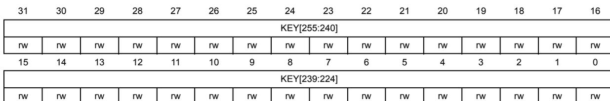
| 31 | 30 | 29 | 28 | 27 | 26 | 25 | 24 | 23 | 22 | 21 | 20 | 19 | 18 | 17 | 16 |
| KEY[255:240] | |||||||||||||||
| rw | rw | rw | rw | rw | rw | rw | rw | rw | rw | rw | rw | rw | rw | rw | rw |
| 15 | 14 | 13 | 12 | 11 | 10 | 9 | 8 | 7 | 6 | 5 | 4 | 3 | 2 | 1 | 0 |
| KEY[239:224] | |||||||||||||||
| rw | rw | rw | rw | rw | rw | rw | rw | rw | rw | rw | rw | rw | rw | rw | rw |
Bits 31:0 KEY[255:224] : Cryptographic key, bits [255:224]
Refer to the AES_KEYR0 register for description of the KEY[255:0] bitfield.
Note: The key registers from 4 to 7 are used only when the key length of 256 bits is selected. They have no effect when the key length of 128 bits is selected (only key registers 0 to 3 are used in that case).
28.7.17 AES suspend registers (AES_SUSPxR)
Address offset: 0x040 + x * 0x4, (x = 0 to 7)
Reset value: 0x0000 0000
These registers contain the complete internal register states of the AES processor when the AES processing of the current task is suspended to process a higher-priority task.
Upon suspend, the software reads and saves the AES_SUSPxR register contents (where x is from 0 to 7) into memory, before using the AES processor for the higher-priority task.
Upon completion, the software restores the saved contents back into the corresponding suspend registers, before resuming the original task.
Note: These registers are used only when GCM, GMAC, or CCM chaining mode is selected.
These registers can be read only when AES is enabled. Reading these registers while AES is disabled returns 0x0000 0000.
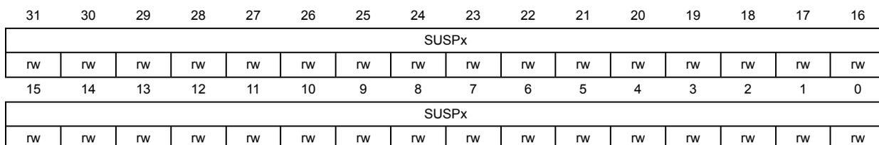
| 31 | 30 | 29 | 28 | 27 | 26 | 25 | 24 | 23 | 22 | 21 | 20 | 19 | 18 | 17 | 16 |
| SUSPx | |||||||||||||||
| rw | rw | rw | rw | rw | rw | rw | rw | rw | rw | rw | rw | rw | rw | rw | rw |
| 15 | 14 | 13 | 12 | 11 | 10 | 9 | 8 | 7 | 6 | 5 | 4 | 3 | 2 | 1 | 0 |
| SUSPx | |||||||||||||||
| rw | rw | rw | rw | rw | rw | rw | rw | rw | rw | rw | rw | rw | rw | rw | rw |
Bits 31:0 SUSPx : AES suspend
Upon suspend operation, this bitfield of every AES_SUSPxR register takes the value of one of internal AES registers.
28.7.18 AES register map
Table 190. AES register map and reset values
| Offset | Register | 31 | 30 | 29 | 28 | 27 | 26 | 25 | 24 | 23 | 22 | 21 | 20 | 19 | 18 | 17 | 16 | 15 | 14 | 13 | 12 | 11 | 10 | 9 | 8 | 7 | 6 | 5 | 4 | 3 | 2 | 1 | 0 |
|---|---|---|---|---|---|---|---|---|---|---|---|---|---|---|---|---|---|---|---|---|---|---|---|---|---|---|---|---|---|---|---|---|---|
| 0x0000 | AES_CR | Res. | Res. | Res. | Res. | Res. | Res. | Res. | Res. | Res. | Res. | Res. | Res. | Res. | KEYSIZE | Res. | CHMOD[2] | Res. | GCMPH[1:0] | DMAOUTEN | DMAINEN | ERRIE | CCFIE | ERRC | CCFC | Res. | CHMOD[1:0] | Res. | MODE[1:0] | Res. | DATATYPE[1:0] | Res. | EN |
| Reset value | 0 | 0 | 0 | 0 | 0 | 0 | 0 | 0 | 0 | 0 | 0 | 0 | 0 | 0 | 0 | 0 | 0 | ||||||||||||||||
| 0x0004 | AES_SR | Res. | Res. | Res. | Res. | Res. | Res. | Res. | Res. | Res. | Res. | Res. | Res. | Res. | Res. | Res. | Res. | Res. | Res. | Res. | Res. | Res. | Res. | Res. | Res. | Res. | Res. | Res. | Res. | BUSY | WRERR | RDERR | CCF |
| Reset value | 0 | 0 | 0 | 0 | |||||||||||||||||||||||||||||
| 0x0008 | AES_DINR x=96,64,32,0 | DIN[x+31:x] | |||||||||||||||||||||||||||||||
| Reset value | 0 | 0 | 0 | 0 | 0 | 0 | 0 | 0 | 0 | 0 | 0 | 0 | 0 | 0 | 0 | 0 | 0 | 0 | 0 | 0 | 0 | 0 | 0 | 0 | 0 | 0 | 0 | 0 | 0 | 0 | 0 | 0 | |
| 0x000C | AES_DOUTR x=96,64,32,0 | DOUT[x+31:x] | |||||||||||||||||||||||||||||||
| Reset value | 0 | 0 | 0 | 0 | 0 | 0 | 0 | 0 | 0 | 0 | 0 | 0 | 0 | 0 | 0 | 0 | 0 | 0 | 0 | 0 | 0 | 0 | 0 | 0 | 0 | 0 | 0 | 0 | 0 | 0 | 0 | 0 | |
| 0x0010 | AES_KEYR0 | KEY[31:0] | |||||||||||||||||||||||||||||||
| Reset value | 0 | 0 | 0 | 0 | 0 | 0 | 0 | 0 | 0 | 0 | 0 | 0 | 0 | 0 | 0 | 0 | 0 | 0 | 0 | 0 | 0 | 0 | 0 | 0 | 0 | 0 | 0 | 0 | 0 | 0 | 0 | 0 | |
| 0x0014 | AES_KEYR1 | KEY[63:32] | |||||||||||||||||||||||||||||||
| Reset value | 0 | 0 | 0 | 0 | 0 | 0 | 0 | 0 | 0 | 0 | 0 | 0 | 0 | 0 | 0 | 0 | 0 | 0 | 0 | 0 | 0 | 0 | 0 | 0 | 0 | 0 | 0 | 0 | 0 | 0 | 0 | 0 | |
| 0x0018 | AES_KEYR2 | KEY[95:64] | |||||||||||||||||||||||||||||||
| Reset value | 0 | 0 | 0 | 0 | 0 | 0 | 0 | 0 | 0 | 0 | 0 | 0 | 0 | 0 | 0 | 0 | 0 | 0 | 0 | 0 | 0 | 0 | 0 | 0 | 0 | 0 | 0 | 0 | 0 | 0 | 0 | 0 | |
| 0x001C | AES_KEYR3 | KEY[127:96] | |||||||||||||||||||||||||||||||
| Reset value | 0 | 0 | 0 | 0 | 0 | 0 | 0 | 0 | 0 | 0 | 0 | 0 | 0 | 0 | 0 | 0 | 0 | 0 | 0 | 0 | 0 | 0 | 0 | 0 | 0 | 0 | 0 | 0 | 0 | 0 | 0 | 0 | |
| 0x0020 | AES_IVR0 | IVI[31:0] | |||||||||||||||||||||||||||||||
| Reset value | 0 | 0 | 0 | 0 | 0 | 0 | 0 | 0 | 0 | 0 | 0 | 0 | 0 | 0 | 0 | 0 | 0 | 0 | 0 | 0 | 0 | 0 | 0 | 0 | 0 | 0 | 0 | 0 | 0 | 0 | 0 | 0 | |
| 0x0024 | AES_IVR1 | IVI[63:32] | |||||||||||||||||||||||||||||||
| Reset value | 0 | 0 | 0 | 0 | 0 | 0 | 0 | 0 | 0 | 0 | 0 | 0 | 0 | 0 | 0 | 0 | 0 | 0 | 0 | 0 | 0 | 0 | 0 | 0 | 0 | 0 | 0 | 0 | 0 | 0 | 0 | 0 | |
| 0x0028 | AES_IVR2 | IVI[95:64] | |||||||||||||||||||||||||||||||
| Reset value | 0 | 0 | 0 | 0 | 0 | 0 | 0 | 0 | 0 | 0 | 0 | 0 | 0 | 0 | 0 | 0 | 0 | 0 | 0 | 0 | 0 | 0 | 0 | 0 | 0 | 0 | 0 | 0 | 0 | 0 | 0 | 0 | |
| 0x002C | AES_IVR3 | IVI[127:96] | |||||||||||||||||||||||||||||||
| Reset value | 0 | 0 | 0 | 0 | 0 | 0 | 0 | 0 | 0 | 0 | 0 | 0 | 0 | 0 | 0 | 0 | 0 | 0 | 0 | 0 | 0 | 0 | 0 | 0 | 0 | 0 | 0 | 0 | 0 | 0 | 0 | 0 | |
| 0x0030 | AES_KEYR4 | KEY[159:128] | |||||||||||||||||||||||||||||||
| Reset value | 0 | 0 | 0 | 0 | 0 | 0 | 0 | 0 | 0 | 0 | 0 | 0 | 0 | 0 | 0 | 0 | 0 | 0 | 0 | 0 | 0 | 0 | 0 | 0 | 0 | 0 | 0 | 0 | 0 | 0 | 0 | 0 | |
| 0x0034 | AES_KEYR5 | KEY[191:160] | |||||||||||||||||||||||||||||||
| Reset value | 0 | 0 | 0 | 0 | 0 | 0 | 0 | 0 | 0 | 0 | 0 | 0 | 0 | 0 | 0 | 0 | 0 | 0 | 0 | 0 | 0 | 0 | 0 | 0 | 0 | 0 | 0 | 0 | 0 | 0 | 0 | 0 | |
| 0x0038 | AES_KEYR6 | KEY[223:192] | |||||||||||||||||||||||||||||||
| Reset value | 0 | 0 | 0 | 0 | 0 | 0 | 0 | 0 | 0 | 0 | 0 | 0 | 0 | 0 | 0 | 0 | 0 | 0 | 0 | 0 | 0 | 0 | 0 | 0 | 0 | 0 | 0 | 0 | 0 | 0 | 0 | 0 | |
Table 190. AES register map and reset values (continued)
| Offset | Register | 31 | 30 | 29 | 28 | 27 | 26 | 25 | 24 | 23 | 22 | 21 | 20 | 19 | 18 | 17 | 16 | 15 | 14 | 13 | 12 | 11 | 10 | 9 | 8 | 7 | 6 | 5 | 4 | 3 | 2 | 1 | 0 |
|---|---|---|---|---|---|---|---|---|---|---|---|---|---|---|---|---|---|---|---|---|---|---|---|---|---|---|---|---|---|---|---|---|---|
| 0x003 C | AES_KEYR7 | KEY[255:224] | |||||||||||||||||||||||||||||||
| Reset value | 0 | 0 | 0 | 0 | 0 | 0 | 0 | 0 | 0 | 0 | 0 | 0 | 0 | 0 | 0 | 0 | 0 | 0 | 0 | 0 | 0 | 0 | 0 | 0 | 0 | 0 | 0 | 0 | 0 | 0 | 0 | 0 | |
| 0x0040 | AES_SUSP0R | SUSP0[31:0] | |||||||||||||||||||||||||||||||
| Reset value | 0 | 0 | 0 | 0 | 0 | 0 | 0 | 0 | 0 | 0 | 0 | 0 | 0 | 0 | 0 | 0 | 0 | 0 | 0 | 0 | 0 | 0 | 0 | 0 | 0 | 0 | 0 | 0 | 0 | 0 | 0 | 0 | |
| 0x0044 | AES_SUSP1R | SUSP1[31:0] | |||||||||||||||||||||||||||||||
| Reset value | 0 | 0 | 0 | 0 | 0 | 0 | 0 | 0 | 0 | 0 | 0 | 0 | 0 | 0 | 0 | 0 | 0 | 0 | 0 | 0 | 0 | 0 | 0 | 0 | 0 | 0 | 0 | 0 | 0 | 0 | 0 | 0 | |
| 0x0048 | AES_SUSP2R | SUSP2[31:0] | |||||||||||||||||||||||||||||||
| Reset value | 0 | 0 | 0 | 0 | 0 | 0 | 0 | 0 | 0 | 0 | 0 | 0 | 0 | 0 | 0 | 0 | 0 | 0 | 0 | 0 | 0 | 0 | 0 | 0 | 0 | 0 | 0 | 0 | 0 | 0 | 0 | 0 | |
| 0x004C | AES_SUSP3R | SUSP3[31:0] | |||||||||||||||||||||||||||||||
| Reset value | 0 | 0 | 0 | 0 | 0 | 0 | 0 | 0 | 0 | 0 | 0 | 0 | 0 | 0 | 0 | 0 | 0 | 0 | 0 | 0 | 0 | 0 | 0 | 0 | 0 | 0 | 0 | 0 | 0 | 0 | 0 | 0 | |
| 0x0050 | AES_SUSP4R | SUSP4[31:0] | |||||||||||||||||||||||||||||||
| Reset value | 0 | 0 | 0 | 0 | 0 | 0 | 0 | 0 | 0 | 0 | 0 | 0 | 0 | 0 | 0 | 0 | 0 | 0 | 0 | 0 | 0 | 0 | 0 | 0 | 0 | 0 | 0 | 0 | 0 | 0 | 0 | 0 | |
| 0x0054 | AES_SUSP5R | SUSP5[31:0] | |||||||||||||||||||||||||||||||
| Reset value | 0 | 0 | 0 | 0 | 0 | 0 | 0 | 0 | 0 | 0 | 0 | 0 | 0 | 0 | 0 | 0 | 0 | 0 | 0 | 0 | 0 | 0 | 0 | 0 | 0 | 0 | 0 | 0 | 0 | 0 | 0 | 0 | |
| 0x0058 | AES_SUSP6R | SUSP6[31:0] | |||||||||||||||||||||||||||||||
| Reset value | 0 | 0 | 0 | 0 | 0 | 0 | 0 | 0 | 0 | 0 | 0 | 0 | 0 | 0 | 0 | 0 | 0 | 0 | 0 | 0 | 0 | 0 | 0 | 0 | 0 | 0 | 0 | 0 | 0 | 0 | 0 | 0 | |
| 0x005C | AES_SUSP7R | SUSP7[31:0] | |||||||||||||||||||||||||||||||
| Reset value | 0 | 0 | 0 | 0 | 0 | 0 | 0 | 0 | 0 | 0 | 0 | 0 | 0 | 0 | 0 | 0 | 0 | 0 | 0 | 0 | 0 | 0 | 0 | 0 | 0 | 0 | 0 | 0 | 0 | 0 | 0 | 0 | |
Refer to Section 2.2 on page 75 for the register boundary addresses.