19. Digital-to-analog converter (DAC)
19.1 Introduction
The DAC module is a 12-bit, voltage output digital-to-analog converter. The DAC can be configured in 8- or 12-bit mode and may be used in conjunction with the DMA controller. In 12-bit mode, the data can be left- or right-aligned. The DAC features two output channels, each with its own converter. In dual DAC channel mode, conversions can be done independently or simultaneously when both channels are grouped together for synchronous update operations. An input reference pin, \( V_{REF+} \) (shared with other analog peripherals) is available for better resolution. An internal reference can also be set on the same input. Refer to voltage reference buffer (VREFBUF) section.
The DACx_OUTy pin can be used as general purpose input/output (GPIO) when the DAC output is disconnected from output pad and connected to on chip peripheral. The DAC output buffer can be optionally enabled to obtain a high drive output current. An individual calibration can be applied on each DAC output channel. The DAC output channels support a low power mode, the Sample and hold mode.
19.2 DAC main features
The DAC main features are the following (see Figure 137: Dual-channel DAC block diagram )
- • One DAC interface, maximum two output channels
- • Left or right data alignment in 12-bit mode
- • Synchronized update capability
- • Noise-wave and Triangular-wave generation
- • Dual DAC channel for independent or simultaneous conversions
- • DMA capability for each channel including DMA underrun error detection
- • External triggers for conversion
- • DAC output channel buffered/unbuffered modes
- • Buffer offset calibration
- • Each DAC output can be disconnected from the DACx_OUTy output pin
- • DAC output connection to on-chip peripherals
- • Sample and hold mode for low power operation in Stop mode
- • Input voltage reference from \( V_{REF+} \) pin or internal VREFBUF reference
Figure 137 shows the block diagram of a DAC channel and Table 124 gives the pin description.
19.3 DAC implementation
Table 123. DAC features| DAC features | DAC1 |
|---|---|
| Dual channel | X |
| Output buffer | X |
| I/O connection | DAC1_OUT1 on PA4, DAC1_OUT2 on PA5 |
| Maximum sampling time | 1 Msps |
| Autonomous mode | - |
| VREF+ pin | X |
19.4 DAC functional description
19.4.1 DAC block diagram
Figure 137. Dual-channel DAC block diagram
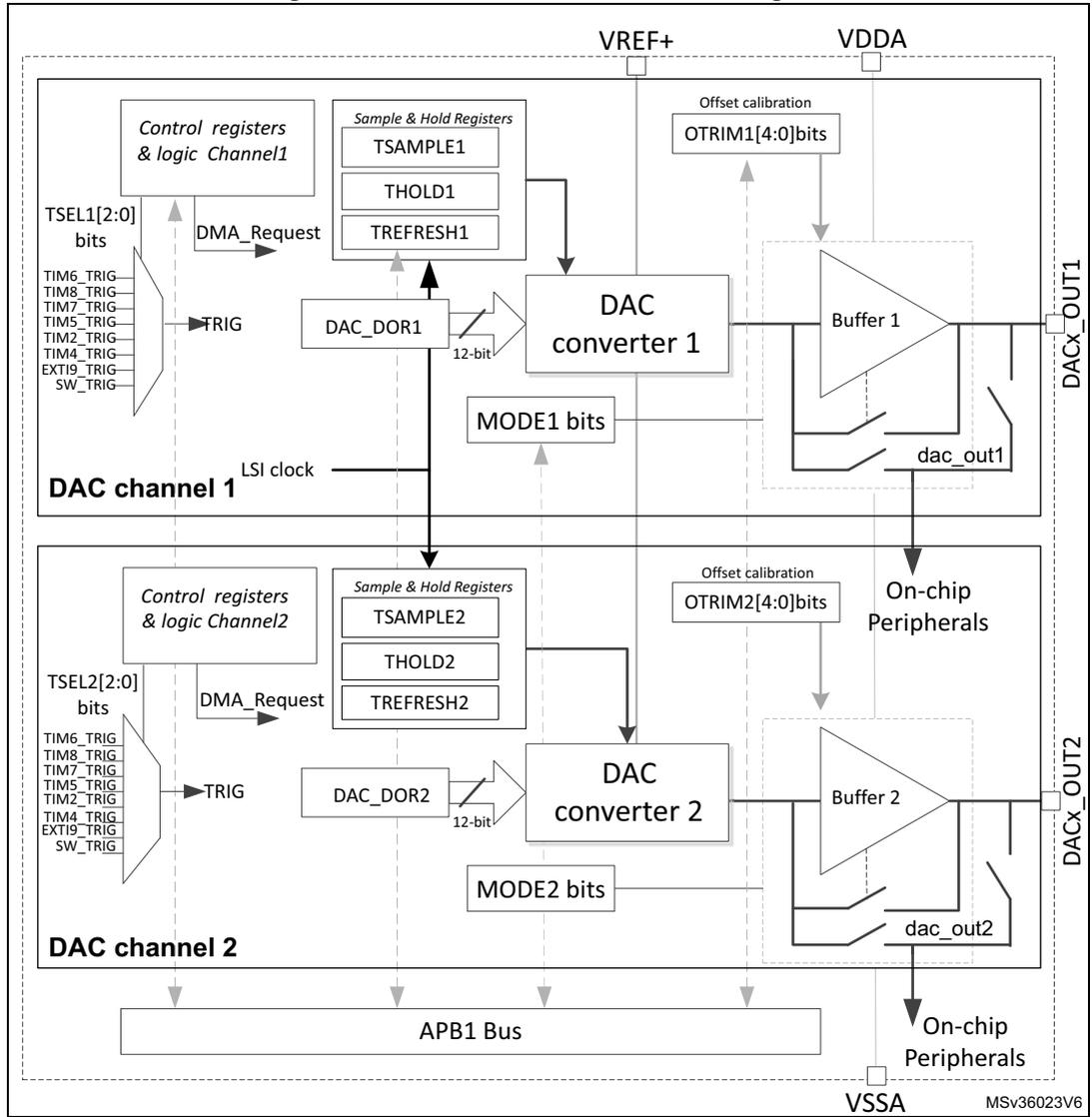
The diagram illustrates the internal architecture of a dual-channel DAC. It is divided into two main sections: DAC channel 1 and DAC channel 2 , both connected to a common APB1 Bus .
- DAC channel 1: Contains Control registers & logic Channel1 and Sample & Hold Registers (TSAMPLE1, THOLD1, TREFRESH1). It features a DAC converter 1 (12-bit) which receives data from DAC_DOR1 . The converter is controlled by MODE1 bits and Offset calibration OTRIM1[4:0] bits . A Buffer 1 is connected to the output DACx_OUT1 (labeled dac_out1 internally). The channel is triggered by TRIG signals from various sources (TIM6_TRIG, TIM8_TRIG, TIM7_TRIG, TIM5_TRIG, TIM2_TRIG, TIM4_TRIG, EXTI9_TRIG, SW_TRIG) selected by TSEL1[2:0] bits . A DMA_Request signal is generated by the control registers. The LSI clock is also connected to this channel.
- DAC channel 2: Similar to Channel 1, it contains Control registers & logic Channel2 and Sample & Hold Registers (TSAMPLE2, THOLD2, TREFRESH2). It features a DAC converter 2 (12-bit) which receives data from DAC_DOR2 . The converter is controlled by MODE2 bits and Offset calibration OTRIM2[4:0] bits . A Buffer 2 is connected to the output DACx_OUT2 (labeled dac_out2 internally). The channel is triggered by TRIG signals from various sources (TIM6_TRIG, TIM8_TRIG, TIM7_TRIG, TIM5_TRIG, TIM2_TRIG, TIM4_TRIG, EXTI9_TRIG, SW_TRIG) selected by TSEL2[2:0] bits . A DMA_Request signal is generated by the control registers.
Power pins VREF+ , VDDA , and VSSA are shown at the top and bottom of the diagram. The identifier MSV36023V6 is located in the bottom right corner.
- 1. MODEx bits in the DAC_MCR control the output mode and allow switching between the Normal mode in buffer/unbuffered configuration and the Sample and hold mode.
- 2. Refer to Section 19.3: DAC implementation for channel2 availability.
The DAC includes:
- • Up to two output channels
- • The DACx_OUTy can be disconnected from the output pin and used as an ordinary GPIO
- • The DAC_OUTx can use an internal pin connection to on-chip peripherals such as comparator, operational amplifier and ADC (if available).
- • DAC output channel buffered or non buffered
- • Sample and hold block and registers operational in Stop mode, using the LSI clock source for static conversion.
The DAC includes up to two separate output channels. Each output channel can be connected to on-chip peripherals such as comparator, operational amplifier and ADC (if available). In this case, the DAC output channel can be disconnected from the DACx_OUTy output pin and the corresponding GPIO can be used for another purpose.
The DAC output can be buffered or not. The Sample and hold block and its associated registers can run in Stop mode using the LSI clock source.
Table 124. DAC input/output pins
| Pin name | Signal type | Remarks |
|---|---|---|
| VREF+ | Input, analog reference positive | The higher/positive reference voltage for the DAC, \( V_{REF+} \leq V_{DDAmax} \) (refer to datasheet) |
| VDDA | Input, analog supply | Analog power supply |
| VSSA | Input, analog supply ground | Ground for analog power supply |
| DACx_OUTy | Analog output signal | DACx channely analog output |
19.4.2 DAC channel enable
Each DAC channel can be powered on by setting its corresponding ENx bit in the DAC_CR register. The DAC channel is then enabled after a \( t_{WAKEUP} \) startup time.
Note: The ENx bit enables the analog DAC channelx only. The DAC channelx digital interface is enabled even if the ENx bit is reset.
19.4.3 DAC data format
Depending on the selected configuration mode, the data have to be written into the specified register as described below:
- • Single DAC channel
There are three possibilities:- – 8-bit right alignment: the software has to load data into the DAC_DHR8Rx[7:0] bits (stored into the DHRx[11:4] bits)
- – 12-bit left alignment: the software has to load data into the DAC_DHR12Lx [15:4] bits (stored into the DHRx[11:0] bits)
- – 12-bit right alignment: the software has to load data into the DAC_DHR12Rx [11:0] bits (stored into the DHRx[11:0] bits)
Depending on the loaded DAC_DHRyyyx register, the data written by the user is shifted and stored into the corresponding DHRx (data holding registerx, which are internal non-memory-
mapped registers). The DHRx register is then loaded into the DORx register either automatically, by software trigger or by an external event trigger.
Figure 138. Data registers in single DAC channel mode
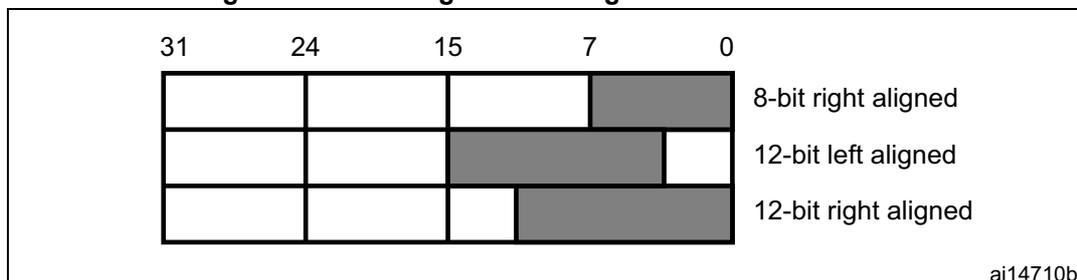
| 31 | 24 | 15 | 7 | 0 | Alignment Mode |
|---|---|---|---|---|---|
| [7:0] | 8-bit right aligned | ||||
| [31:20] | 12-bit left aligned | ||||
| [11:0] | 12-bit right aligned | ||||
ai14710b
- • Dual DAC channels (when available)
There are three possibilities:
- – 8-bit right alignment: data for DAC channel1 to be loaded into the DAC_DHR8RD [7:0] bits (stored into the DHR1[11:4] bits) and data for DAC channel2 to be loaded into the DAC_DHR8RD [15:8] bits (stored into the DHR2[11:4] bits)
- – 12-bit left alignment: data for DAC channel1 to be loaded into the DAC_DHR12LD [15:4] bits (stored into the DHR1[11:0] bits) and data for DAC channel2 to be loaded into the DAC_DHR12LD [31:20] bits (stored into the DHR2[11:0] bits)
- – 12-bit right alignment: data for DAC channel1 to be loaded into the DAC_DHR12RD [11:0] bits (stored into the DHR1[11:0] bits) and data for DAC channel2 to be loaded into the DAC_DHR12RD [27:16] bits (stored into the DHR2[11:0] bits)
Depending on the loaded DAC_DHRyyyD register, the data written by the user is shifted and stored into DHR1 and DHR2 (data holding registers, which are internal non-memory-mapped registers). The DHR1 and DHR2 registers are then loaded into the DAC_DOR1 and DOR2 registers, respectively, either automatically, by software trigger or by an external event trigger.
Figure 139. Data registers in dual DAC channel mode
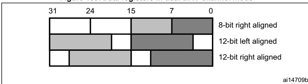
| 31 | 24 | 15 | 7 | 0 | Alignment Mode |
|---|---|---|---|---|---|
| CH2[15:8] | CH1[7:0] | 8-bit right aligned | |||
| CH2[31:20] | CH1[15:4] | 12-bit left aligned | |||
| CH2[27:16] | CH1[11:0] | 12-bit right aligned | |||
ai14709b
19.4.4 DAC conversion
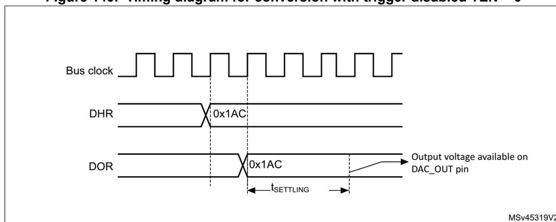
The DAC_DORx cannot be written directly and any data transfer to the DAC channels must be performed by loading the DAC_DHRx register (write operation to DAC_DHR8Rx, DAC_DHR12Lx, DAC_DHR12Rx, DAC_DHR8RD, DAC_DHR12RD or DAC_DHR12LD).
Data stored in the DAC_DHRx register are automatically transferred to the DAC_DORx register after one APB1 clock cycle, if no hardware trigger is selected (TENx bit in DAC_CR register is reset). However, when a hardware trigger is selected (TENx bit in DAC_CR register is set) and a trigger occurs, the transfer is performed three APB1 clock cycles after the trigger signal.
When DAC_DORx is loaded with the DAC_DHRx contents, the analog output voltage becomes available after a time \( t_{\text{SETTLING}} \) that depends on the power supply voltage and the analog output load.
Figure 140. Timing diagram for conversion with trigger disabled TEN = 0
19.4.5 DAC output voltage
Digital inputs are converted to output voltages on a linear conversion between 0 and \( V_{\text{REF+}} \) .
The analog output voltages on each DAC channel pin are determined by the following equation:
19.4.6 DAC trigger selection
If the TENx control bit is set, the conversion can then be triggered by an external event (timer counter, external interrupt line). The TSELx[2:0] control bits determine which out of 8 possible events triggers the conversion as shown in TSELx[2:0] bits of the DAC_CR register. These events can be either the software trigger or hardware triggers.
Each time a DAC interface detects a rising edge on the selected trigger source (refer to the table below), the last data stored into the DAC_DHRx register are transferred into the DAC_DORx register. The DAC_DORx register is updated three APB1 cycles after the trigger occurs.
If the software trigger is selected, the conversion starts once the SWTRIG bit is set. SWTRIG is reset by hardware once the DAC_DORx register has been loaded with the DAC_DHRx register contents.
Note: TSELx[2:0] bit cannot be changed when the ENx bit is set.
When software trigger is selected, the transfer from the DAC_DHRx register to the DAC_DORx register takes only one APB1 clock cycle.
Table 125. DAC trigger selection
| Source | Type | TSELx[2:0] |
|---|---|---|
| TIM6_TRGO | Internal signal from on-chip timers | 000 |
| TIM8_TRGO | Internal signal from on-chip timers | 001 |
| TIM7_TRGO | Internal signal from on-chip timers | 010 |
| TIM5_TRGO | Internal signal from on-chip timers | 011 |
| TIM2_TRGO | Internal signal from on-chip timers | 100 |
| TIM4_TRGO | Internal signal from on-chip timers | 101 |
| EXTI9 | External pin | 110 |
| SWTRIG | Software control bit | 111 |
19.4.7 DMA requests
Each DAC channel has a DMA capability. Two DMA channels are used to service DAC channel DMA requests.
When an external trigger (but not a software trigger) occurs while the DMAENx bit is set, the value of the DAC_DHRx register is transferred into the DAC_DORx register when the transfer is complete, and a DMA request is generated.
In dual mode, if both DMAENx bits are set, two DMA requests are generated. If only one DMA request is needed, only the corresponding DMAENx bit must be set. In this way, the application can manage both DAC channels in dual mode by using one DMA request and a unique DMA channel.
As DAC_DHRx to DAC_DORx data transfer occurred before the DMA request, the very first data has to be written to the DAC_DHRx before the first trigger event occurs.
DMA underrun
The DAC DMA request is not queued so that if a second external trigger arrives before the acknowledgment for the first external trigger is received (first request), then no new request is issued and the DMA channelx underrun flag DMAUDRx in the DAC_SR register is set, reporting the error condition. The DAC channelx continues to convert old data.
The software must clear the DMAUDRx flag by writing 1, clear the DMAEN bit of the used DMA stream and re-initialize both DMA and DAC channelx to restart the transfer correctly. The software must modify the DAC trigger conversion frequency or lighten the DMA workload to avoid a new DMA underrun. Finally, the DAC conversion can be resumed by enabling both DMA data transfer and conversion trigger.
For each DAC channelx, an interrupt is also generated if its corresponding DMAUDRIEx bit in the DAC_CR register is enabled.
19.4.8 Noise generation
In order to generate a variable-amplitude pseudonoise, an LFSR (linear feedback shift register) is available. DAC noise generation is selected by setting WAVEx[1:0] to 01. The preloaded value in LFSR is 0xAAA. This register is updated three APB1 clock cycles after each trigger event, following a specific calculation algorithm.
Figure 141. DAC LFSR register calculation algorithm
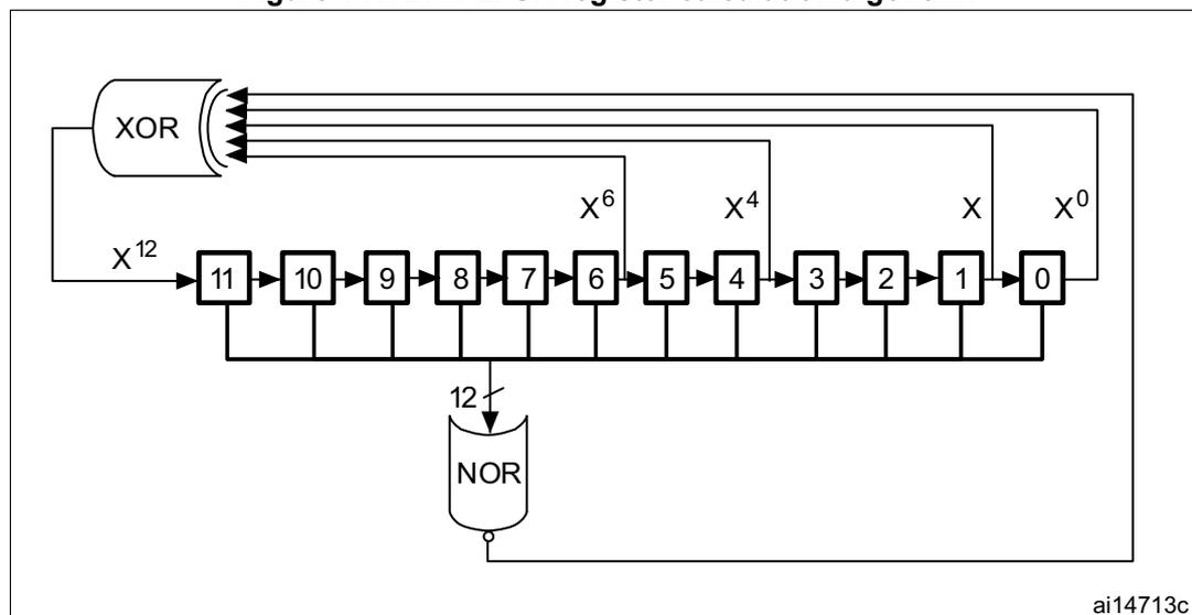
The LFSR value, that may be masked partially or totally by means of the MAMPx[3:0] bits in the DAC_CR register, is added up to the DAC_DHRx contents without overflow and this value is then transferred into the DAC_DORx register.
If LFSR is 0x0000, a '1' is injected into it (antilock-up mechanism).
It is possible to reset LFSR wave generation by resetting the WAVEx[1:0] bits.
Figure 142. DAC conversion (SW trigger enabled) with LFSR wave generation
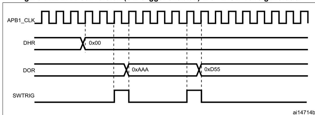
Note: The DAC trigger must be enabled for noise generation by setting the TENx bit in the DAC_CR register.
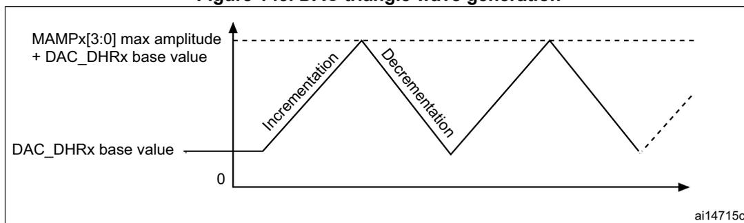
19.4.9 Triangle-wave generation
It is possible to add a small-amplitude triangular waveform on a DC or slowly varying signal. DAC triangle-wave generation is selected by setting WAVEx[1:0] to 10 11 . The amplitude is configured through the MAMPx[3:0] bits in the DAC_CR register. An internal triangle counter is incremented three APB1 clock cycles after each trigger event. The value of this counter is then added to the DAC_DHRx register without overflow and the sum is transferred into the DAC_DORx register. The triangle counter is incremented as long as it is less than the maximum amplitude defined by the MAMPx[3:0] bits. Once the configured amplitude is reached, the counter is decremented down to 0, then incremented again and so on.
It is possible to reset triangle wave generation by resetting the WAVEx[1:0] bits.
Figure 143. DAC triangle wave generation
The graph shows a triangular waveform. The vertical axis represents the DAC output level, with a horizontal line labeled 'DAC_DHRx base value' and a dashed horizontal line at the top labeled 'MAMPx[3:0] max amplitude + DAC_DHRx base value'. The origin is marked '0'. The waveform starts at the base value, rises linearly (labeled 'Incrementation'), reaches the maximum amplitude, falls linearly (labeled 'Decrementation'), reaches a minimum below the base value, and then rises again. The label 'ai14715c' is in the bottom right corner.
Figure 144. DAC conversion (SW trigger enabled) with triangle wave generation
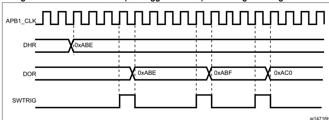
The timing diagram shows four signals over time. The top signal is 'APB1_CLK', a periodic square wave. Below it is 'DHR', which is initially '0xABE' and then changes to '0xABF' and '0xAC0' at specific clock edges. Below 'DHR' is 'DOR', which follows the 'DHR' values. The bottom signal is 'SWTRIG', a pulse that triggers the changes in 'DHR' and 'DOR'. Vertical dashed lines indicate the relationship between clock edges and signal changes. The label 'ai14716b' is in the bottom right corner.
Note: The DAC trigger must be enabled for triangle wave generation by setting the TENx bit in the DAC_CR register.
The MAMPx[3:0] bits must be configured before enabling the DAC, otherwise they cannot be changed.
19.4.10 DAC channel modes
Each DAC channel can be configured in Normal mode or Sample and hold mode. The output buffer can be enabled to obtain a high drive capability. Before enabling output buffer, the voltage offset needs to be calibrated. This calibration is performed at the factory (loaded after reset) and can be adjusted by software during application operation.
Normal mode
In Normal mode, there are four combinations, by changing the buffer state and by changing the DACx_OUTy pin interconnections.
To enable the output buffer, the MODEx[2:0] bits in DAC_MCR register must be:
- • 000: DAC is connected to the external pin
- • 001: DAC is connected to external pin and to on-chip peripherals
To disable the output buffer, the MODEx[2:0] bits in DAC_MCR register must be:
- • 010: DAC is connected to the external pin
- • 011: DAC is connected to on-chip peripherals
Sample and hold mode
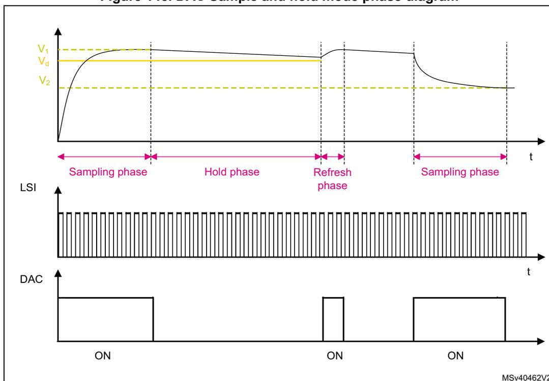
In Sample and hold mode, the DAC core converts data on a triggered conversion, and then holds the converted voltage on a capacitor. When not converting, the DAC cores and buffer are completely turned off between samples and the DAC output is tri-stated, therefore reducing the overall power consumption. A stabilization period, which value depends on the buffer state, is required before each new conversion.
In this mode, the DAC core and all corresponding logic and registers are driven by the LSI low-speed clock in addition to the APB1 clock, allowing using the DAC channels in deep low power modes such as Stop mode.
The LSI low-speed clock must not be stopped when the Sample and hold mode is enabled.
The sample/hold mode operations can be divided into 3 phases:
- 1. Sample phase: the sample/hold element is charged to the desired voltage. The charging time depends on capacitor value (internal or external, selected by the user). The sampling time is configured with the TSAMPLEx[9:0] bits in DAC_SHSRx register. During the write of the TSAMPLEx[9:0] bits, the BWSTx bit in DAC_SR register is set to 1 to synchronize between both clocks domains (APB and low speed clock) and allowing the software to change the value of sample phase during the DAC channel operation
- 2. Hold phase: the DAC output channel is tri-stated, the DAC core and the buffer are turned off, to reduce the current consumption. The hold time is configured with the THOLDx[9:0] bits in DAC_SHHR register
- 3. Refresh phase: the refresh time is configured with the TREFRESHx[7:0] bits in DAC_SHRR register
The timings for the three phases above are in units of LSI clock periods. As an example, to configure a sample time of 350 µs, a hold time of 2 ms and a refresh time of 100 µs assuming LSI ~32 KHz is selected:
12 cycles are required for sample phase: TSAMPLEx[9:0] = 11,
62 cycles are required for hold phase: THOLDx[9:0] = 62,
and 4 cycles are required for refresh period: TREFRESHx[7:0] = 4.
In this example, the power consumption is reduced by almost a factor of 15 versus Normal modes.
The formulas to compute the right sample and refresh timings are described in the table below, the Hold time depends on the leakage current.
Table 126. Sample and refresh timings
| Buffer State | \( t_{\text{SAMP}}^{(1)(2)} \) | \( t_{\text{REFRESH}}^{(2)(3)} \) |
|---|---|---|
| Enable | \( 7 \mu\text{s} + (10 * R_{\text{BON}} * C_{\text{SH}}) \) | \( 7 \mu\text{s} + (R_{\text{BON}} * C_{\text{SH}}) * \ln(2 * N_{\text{LSB}}) \) |
| Disable | \( 3 \mu\text{s} + (10 * R_{\text{BOFF}} * C_{\text{SH}}) \) | \( 3 \mu\text{s} + (R_{\text{BOFF}} * C_{\text{SH}}) * \ln(2 * N_{\text{LSB}}) \) |
- 1. In the above formula the settling to the desired code value with \( \frac{1}{2} \) LSB or accuracy requires 10 constant time for 12 bits resolution. For 8 bits resolution, the settling time is 7 constant time.
- 2. \( C_{\text{SH}} \) is the capacitor in Sample and hold mode.
- 3. The tolerated voltage drop during the hold phase "Vd" is represented by the number of LSBs after the capacitor discharging with the output leakage current. The settling back to the desired value with \( \frac{1}{2} \) LSB error accuracy requires \( \ln(2 * N_{\text{lsb}}) \) constant time of the DAC.
Example of the sample and refresh time calculation with output buffer on
The values used in the example below are provided as indication only. Refer to the product datasheet for product data.
Sampling phase:
(where \( R_{\text{BON}} = 2 \text{ k}\Omega \) )
Refresh phase:
(where \( N_{\text{LSB}} = 10 \) (10 LSB drop during the hold phase))
Hold phase:
Figure 145. DAC Sample and hold mode phase diagram
Like in Normal mode, the Sample and hold mode has different configurations.
To enable the output buffer, MODE x [2:0] bits in DAC_MCR register must be set to:
- • 100: DAC is connected to the external pin
- • 101: DAC is connected to external pin and to on chip peripherals
To disabled the output buffer, MODE x [2:0] bits in DAC_MCR register must be set to:
- • 110: DAC is connected to external pin and to on chip peripherals
- • 111: DAC is connected to on chip peripherals
When MODE x [2:0] bits are equal to 111, an internal capacitor, \( C_{Lint} \) , holds the voltage output of the DAC core and then drive it to on-chip peripherals.
All Sample and hold phases are interruptible, and any change in DAC_DHRx immediately triggers a new sample phase.
Table 127. Channel output modes summary
| MODE x [2:0] | Mode | Buffer | Output connections | ||
|---|---|---|---|---|---|
| 0 | 0 | 0 | Normal mode | Enabled | Connected to external pin |
| 0 | 0 | 1 | Connected to external pin and to on chip-peripherals (such as comparators) | ||
| 0 | 1 | 0 | Disabled | Connected to external pin | |
| 0 | 1 | 1 | Connected to on chip peripherals (such as comparators) | ||
Table 127. Channel output modes summary (continued)
| MODEx[2:0] | Mode | Buffer | Output connections | ||
|---|---|---|---|---|---|
| 1 | 0 | 0 | Sample and hold mode | Enabled | Connected to external pin |
| 1 | 0 | 1 | Connected to external pin and to on chip peripherals (such as comparators) | ||
| 1 | 1 | 0 | Disabled | Connected to external pin and to on chip peripherals (such as comparators) | |
| 1 | 1 | 1 | Connected to on chip peripherals (such as comparators) | ||
19.4.11 DAC channel buffer calibration
The transfer function for an N-bit digital-to-analog converter (DAC) is:
Where \( V_{OUT} \) is the analog output, \( D \) is the digital input, \( G \) is the gain, \( V_{ref} \) is the nominal full-scale voltage, and \( V_{os} \) is the offset voltage. For an ideal DAC channel, \( G = 1 \) and \( V_{os} = 0 \) .
Due to output buffer characteristics, the voltage offset may differ from part-to-part and introduce an absolute offset error on the analog output. To compensate the \( V_{os} \) , a calibration is required by a trimming technique.
The calibration is only valid when the DAC channelx is operating with buffer enabled (MODEx[2:0] = 0b000 or 0b001 or 0b100 or 0b101). if applied in other modes when the buffer is off, it has no effect. During the calibration:
- • The buffer output is disconnected from the pin internal/external connections and put in tristate mode (HiZ).
- • The buffer acts as a comparator to sense the middle-code value 0x800 and compare it to VREF+/2 signal through an internal bridge, then toggle its output signal to 0 or 1 depending on the comparison result (CAL_FLAGx bit).
Two calibration techniques are provided:
- • Factory trimming (default setting)
The DAC buffer offset is factory trimmed. The default value of OTRIMx[4:0] bits in DAC_CCR register is the factory trimming value and it is loaded once DAC digital interface is reset.
- • User trimming
The user trimming can be done when the operating conditions differs from nominal factory trimming conditions and in particular when \( V_{DDA} \) voltage, temperature, VREF+ values change and can be done at any point during application by software.
Note: Refer to the datasheet for more details of the Nominal factory trimming conditions
In addition, when \( V_{DD} \) is removed (example the device enters in STANDBY or VBAT modes) the calibration is required.
The steps to perform a user trimming calibration are as below:
- 1. If the DAC channel is active, write 0 to ENx bit in DAC_CR to disable the channel.
- 2. Select a mode where the buffer is enabled, by writing to DAC_MCR register, MODEx[2:0] = 0b000 or 0b001 or 0b100 or 0b101.
- 3. Start the DAC channelx calibration, by setting the CENx bit in DAC_CR register to 1.
- 4. Apply a trimming algorithm:
- a) Write a code into OTRIMx[4:0] bits, starting by 0b00000.
- b) Wait for \( t_{TRIM} \) delay.
- c) Check if CAL_FLAGx bit in DAC_SR is set to 1.
- d) If CAL_FLAGx is set to 1, the OTRIMx[4:0] trimming code is found and can be used during device operation to compensate the output value, else increment OTRIMx[4:0] and repeat sub-steps from (a) to (d) again.
The software algorithm may use either a successive approximation or dichotomy techniques to compute and set the content of OTRIMx[4:0] bits in a faster way.
The commutation/toggle of CAL_FLAGx bit indicates that the offset is correctly compensated and the corresponding trim code must be kept in the OTRIMx[4:0] bits in DAC_CCR register.
Note: A \( t_{TRIM} \) delay must be respected between the write to the OTRIMx[4:0] bits and the read of the CAL_FLAGx bit in DAC_SR register in order to get a correct value. This parameter is specified into datasheet electrical characteristics section.
If \( V_{DDA} \) , \( V_{REF+} \) and temperature conditions do not change during device operation while it enters more often in standby and VBAT mode, the software may store the OTRIMx[4:0] bits found in the first user calibration in the flash or in back-up registers. then to load/write them directly when the device power is back again thus avoiding to wait for a new calibration time.
When CENx bit is set, it is not allowed to set ENx bit.
19.4.12 Dual DAC channel conversion modes (if dual channels are available)
To efficiently use the bus bandwidth in applications that require the two DAC channels at the same time, three dual registers are implemented: DHR8RD, DHR12RD and DHR12LD. A unique register access is then required to drive both DAC channels at the same time. For the wave generation, no accesses to DHRxxxD registers are required. As a result, two output channels can be used either independently or simultaneously.
11 conversion modes are possible using the two DAC channels and these dual registers. All the conversion modes can nevertheless be obtained using separate DHRx registers if needed.
All modes are described in the paragraphs below.
Independent trigger without wave generation
To configure the DAC in this conversion mode, the following sequence is required:
- 1. Set the two DAC channel trigger enable bits TEN1 and TEN2.
- 2. Configure different trigger sources by setting different values in the TSEL1 and TSEL2 bitfields.
- 3. Load the dual DAC channel data into the desired DHR register (DAC_DHR12RD, DAC_DHR12LD or DAC_DHR8RD).
When a DAC channel1 trigger arrives, the DHR1 register is transferred into DAC_DOR1 (three APB1 clock cycles later).
When a DAC channel2 trigger arrives, the DHR2 register is transferred into DAC_DOR2 (three APB1 clock cycles later).
Independent trigger with single LFSR generation
To configure the DAC in this conversion mode, the following sequence is required:
- 1. Set the two DAC channel trigger enable bits TEN1 and TEN2.
- 2. Configure different trigger sources by setting different values in the TSEL1 and TSEL2 bitfields.
- 3. Configure the two DAC channel WAVEx[1:0] bits as 01 and the same LFSR mask value in the MAMPx[3:0] bits.
- 4. Load the dual DAC channel data into the desired DHR register (DAC_DHR12RD, DAC_DHR12LD or DAC_DHR8RD).
When a DAC channel1 trigger arrives, the LFSR1 counter, with the same mask, is added to the DHR1 register and the sum is transferred into DAC_DOR1 (three APB1 clock cycles later). Then the LFSR1 counter is updated.
When a DAC channel2 trigger arrives, the LFSR2 counter, with the same mask, is added to the DHR2 register and the sum is transferred into DAC_DOR2 (three APB1 clock cycles later). Then the LFSR2 counter is updated.
Independent trigger with different LFSR generation
To configure the DAC in this conversion mode, the following sequence is required:
- 1. Set the two DAC channel trigger enable bits TEN1 and TEN2.
- 2. Configure different trigger sources by setting different values in the TSEL1 and TSEL2 bitfields.
- 3. Configure the two DAC channel WAVEx[1:0] bits as 01 and set different LFSR masks values in the MAMP1[3:0] and MAMP2[3:0] bits.
- 4. Load the dual DAC channel data into the desired DHR register (DAC_DHR12RD, DAC_DHR12LD or DAC_DHR8RD).
When a DAC channel1 trigger arrives, the LFSR1 counter, with the mask configured by MAMP1[3:0], is added to the DHR1 register and the sum is transferred into DAC_DOR1 (three APB1 clock cycles later). Then the LFSR1 counter is updated.
When a DAC channel2 trigger arrives, the LFSR2 counter, with the mask configured by MAMP2[3:0], is added to the DHR2 register and the sum is transferred into DAC_DOR2 (three APB1 clock cycles later). Then the LFSR2 counter is updated.
Independent trigger with single triangle generation
To configure the DAC in this conversion mode, the following sequence is required:
- 1. Set the two DAC channel trigger enable bits TEN1 and TEN2.
- 2. Configure different trigger sources by setting different values in the TSEL1 and TSEL2 bitfields.
- 3. Configure the two DAC channel WAVEx[1:0] bits as 1x and the same maximum amplitude value in the MAMPx[3:0] bits.
- 4. Load the dual DAC channel data into the desired DHR register (DAC_DHR12RD, DAC_DHR12LD or DAC_DHR8RD).
When a DAC channel1 trigger arrives, the DAC channel1 triangle counter, with the same triangle amplitude, is added to the DHR1 register and the sum is transferred into DAC_DOR1 (three APB1 clock cycles later). The DAC channel1 triangle counter is then updated.
When a DAC channel2 trigger arrives, the DAC channel2 triangle counter, with the same triangle amplitude, is added to the DHR2 register and the sum is transferred into DAC_DOR2 (three APB1 clock cycles later). The DAC channel2 triangle counter is then updated.
Independent trigger with different triangle generation
To configure the DAC in this conversion mode, the following sequence is required:
- 1. Set the two DAC channel trigger enable bits TEN1 and TEN2.
- 2. Configure different trigger sources by setting different values in the TSEL1 and TSEL2 bits.
- 3. Configure the two DAC channel WAVEx[1:0] bits as 1x and set different maximum amplitude values in the MAMP1[3:0] and MAMP2[3:0] bits.
- 4. Load the dual DAC channel data into the desired DHR register (DAC_DHR12RD, DAC_DHR12LD or DAC_DHR8RD).
When a DAC channel1 trigger arrives, the DAC channel1 triangle counter, with a triangle amplitude configured by MAMP1[3:0], is added to the DHR1 register and the sum is transferred into DAC_DOR1 (three APB1 clock cycles later). The DAC channel1 triangle counter is then updated.
When a DAC channel2 trigger arrives, the DAC channel2 triangle counter, with a triangle amplitude configured by MAMP2[3:0], is added to the DHR2 register and the sum is transferred into DAC_DOR2 (three APB1 clock cycles later). The DAC channel2 triangle counter is then updated.
Simultaneous software start
To configure the DAC in this conversion mode, the following sequence is required:
- • Load the dual DAC channel data to the desired DHR register (DAC_DHR12RD, DAC_DHR12LD or DAC_DHR8RD).
In this configuration, one APB1 clock cycle later, the DHR1 and DHR2 registers are transferred into DAC_DOR1 and DAC_DOR2, respectively.
Simultaneous trigger without wave generation
To configure the DAC in this conversion mode, the following sequence is required:
- 1. Set the two DAC channel trigger enable bits TEN1 and TEN2.
- 2. Configure the same trigger source for both DAC channels by setting the same value in the TSEL1 and TSEL2 bitfields.
- 3. Load the dual DAC channel data to the desired DHR register (DAC_DHR12RD, DAC_DHR12LD or DAC_DHR8RD).
When a trigger arrives, the DHR1 and DHR2 registers are transferred into DAC_DOR1 and DAC_DOR2, respectively (after three APB1 clock cycles).
Simultaneous trigger with single LFSR generation
- 1. To configure the DAC in this conversion mode, the following sequence is required:
- 2. Set the two DAC channel trigger enable bits TEN1 and TEN2.
- 3. Configure the same trigger source for both DAC channels by setting the same value in the TSEL1 and TSEL2 bitfields.
- 4. Configure the two DAC channel WAVEx[1:0] bits as 01 and the same LFSR mask value in the MAMPx[3:0] bits.
- 5. Load the dual DAC channel data to the desired DHR register (DHR12RD, DHR12LD or DHR8RD).
When a trigger arrives, the LFSR1 counter, with the same mask, is added to the DHR1 register and the sum is transferred into DAC_DOR1 (three APB1 clock cycles later). The LFSR1 counter is then updated. At the same time, the LFSR2 counter, with the same mask, is added to the DHR2 register and the sum is transferred into DAC_DOR2 (three APB1 clock cycles later). The LFSR2 counter is then updated.
Simultaneous trigger with different LFSR generation
To configure the DAC in this conversion mode, the following sequence is required:
- 1. Set the two DAC channel trigger enable bits TEN1 and TEN2
- 2. Configure the same trigger source for both DAC channels by setting the same value in the TSEL1 and TSEL2 bitfields.
- 3. Configure the two DAC channel WAVEx[1:0] bits as 01 and set different LFSR mask values using the MAMP1[3:0] and MAMP2[3:0] bits.
- 4. Load the dual DAC channel data into the desired DHR register (DAC_DHR12RD, DAC_DHR12LD or DAC_DHR8RD).
When a trigger arrives, the LFSR1 counter, with the mask configured by MAMP1[3:0], is added to the DHR1 register and the sum is transferred into DAC_DOR1 (three APB1 clock cycles later). The LFSR1 counter is then updated.
At the same time, the LFSR2 counter, with the mask configured by MAMP2[3:0], is added to the DHR2 register and the sum is transferred into DAC_DOR2 (three APB1 clock cycles later). The LFSR2 counter is then updated.
Simultaneous trigger with single triangle generation
To configure the DAC in this conversion mode, the following sequence is required:
- 1. Set the two DAC channel trigger enable bits TEN1 and TEN2
- 2. Configure the same trigger source for both DAC channels by setting the same value in the TSEL1 and TSEL2 bitfields.
- 3. Configure the two DAC channel WAVEx[1:0] bits as 1x and the same maximum amplitude value using the MAMPx[3:0] bits.
- 4. Load the dual DAC channel data into the desired DHR register (DAC_DHR12RD, DAC_DHR12LD or DAC_DHR8RD).
When a trigger arrives, the DAC channel1 triangle counter, with the same triangle amplitude, is added to the DHR1 register and the sum is transferred into DAC_DOR1 (three APB1 clock cycles later). The DAC channel1 triangle counter is then updated.
At the same time, the DAC channel2 triangle counter, with the same triangle amplitude, is added to the DHR2 register and the sum is transferred into DAC_DOR2 (three APB1 clock cycles later). The DAC channel2 triangle counter is then updated.
Simultaneous trigger with different triangle generation
To configure the DAC in this conversion mode, the following sequence is required:
- 1. Set the two DAC channel trigger enable bits TEN1 and TEN2
- 2. Configure the same trigger source for both DAC channels by setting the same value in the TSEL1 and TSEL2 bitfields.
- 3. Configure the two DAC channel WAVEx[1:0] bits as 1x and set different maximum amplitude values in the MAMP1[3:0] and MAMP2[3:0] bits.
- 4. Load the dual DAC channel data into the desired DHR register (DAC_DHR12RD, DAC_DHR12LD or DAC_DHR8RD).
When a trigger arrives, the DAC channel1 triangle counter, with a triangle amplitude configured by MAMP1[3:0], is added to the DHR1 register and the sum is transferred into DAC_DOR1 (three APB clock cycles later). Then the DAC channel1 triangle counter is updated.
At the same time, the DAC channel2 triangle counter, with a triangle amplitude configured by MAMP2[3:0], is added to the DHR2 register and the sum is transferred into DAC_DOR2 (three APB1 clock cycles later). Then the DAC channel2 triangle counter is updated.
19.5 DAC in low-power modes
Table 128. Effect of low-power modes on DAC
| Mode | Description |
|---|---|
| Sleep | No effect, DAC used with DMA |
| Low-power run | No effect. |
| Low-power sleep | No effect. DAC used with DMA. |
| Stop 0 / Stop 1 | The DAC remains active with a static value if the Sample and hold mode is selected using LSI clock. |
| Stop 2 | The DAC registers content is kept. The DAC must be disabled before entering Stop 2. |
Table 128. Effect of low-power modes on DAC (continued)
| Mode | Description |
|---|---|
| Standby | The DAC peripheral is powered down and must be reinitialized after exiting Standby or Shutdown mode. |
| Shutdown |
19.6 DAC interrupts
Table 129. DAC interrupts
| Interrupt acronym | Interrupt event | Event flag | Enable control bit | Interrupt clear method | Exit Sleep mode | Exit Stop mode | Exit Standby mode |
|---|---|---|---|---|---|---|---|
| DAC | DMA underrun | DMAUDRx | DMAUDRI Ex | Write DMAUDRx = 1 | Yes | No | No |
19.7 DAC registers
Refer to Section 1 on page 69 for a list of abbreviations used in register descriptions.
The peripheral registers have to be accessed by words (32-bit).
19.7.1 DAC control register (DAC_CR)
Address offset: 0x00
Reset value: 0x0000 0000
| 31 | 30 | 29 | 28 | 27 | 26 | 25 | 24 | 23 | 22 | 21 | 20 | 19 | 18 | 17 | 16 |
|---|---|---|---|---|---|---|---|---|---|---|---|---|---|---|---|
| Res. | CEN2 | DMAUDRIE2 | DMAEN2 | MAMP2[3:0] | WAVE2[1:0] | TSEL2[2] | TSEL2[1] | TSEL2[0] | TEN2 | Res. | EN2 | ||||
| rw | rw | rw | rw | rw | rw | rw | rw | rw | rw | rw | rw | rw | rw | ||
| 15 | 14 | 13 | 12 | 11 | 10 | 9 | 8 | 7 | 6 | 5 | 4 | 3 | 2 | 1 | 0 |
|---|---|---|---|---|---|---|---|---|---|---|---|---|---|---|---|
| Res. | CEN1 | DMAUDRIE1 | DMAEN1 | MAMP1[3:0] | WAVE1[1:0] | TSEL1[2] | TSEL1[1] | TSEL1[0] | TEN1 | Res. | EN1 | ||||
| rw | rw | rw | rw | rw | rw | rw | rw | rw | rw | rw | rw | rw | rw | ||
Bit 31 Reserved, must be kept at reset value.
Bit 30 CEN2 : DAC channel2 calibration enable
This bit is set and cleared by software to enable/disable DAC channel2 calibration, it can be written only if EN2 bit is set to 0 into DAC_CR (the calibration mode can be entered/exit only when the DAC channel is disabled) Otherwise, the write operation is ignored.
0: DAC channel2 in Normal operating mode
1: DAC channel2 in calibration mode
Note: This bit is available only on dual-channel DACs. Refer to Section 19.3: DAC implementation .
Bit 29 DMAUDRIE2 : DAC channel2 DMA underrun interrupt enable
This bit is set and cleared by software.
0: DAC channel2 DMA underrun interrupt disabled
1: DAC channel2 DMA underrun interrupt enabled
Note: This bit is available only on dual-channel DACs. Refer to Section 19.3: DAC implementation .
Bit 28 DMAEN2 : DAC channel2 DMA enable
This bit is set and cleared by software.
0: DAC channel2 DMA mode disabled
1: DAC channel2 DMA mode enabled
Note: This bit is available only on dual-channel DACs. Refer to Section 19.3: DAC implementation .
Bits 27:24 MAMP2[3:0] : DAC channel2 mask/amplitude selectorThese bits are written by software to select mask in wave generation mode or amplitude in triangle generation mode.
0000: Unmask bit0 of LFSR/ triangle amplitude equal to 1
0001: Unmask bits[1:0] of LFSR/ triangle amplitude equal to 3
0010: Unmask bits[2:0] of LFSR/ triangle amplitude equal to 7
0011: Unmask bits[3:0] of LFSR/ triangle amplitude equal to 15
0100: Unmask bits[4:0] of LFSR/ triangle amplitude equal to 31
0101: Unmask bits[5:0] of LFSR/ triangle amplitude equal to 63
0110: Unmask bits[6:0] of LFSR/ triangle amplitude equal to 127
0111: Unmask bits[7:0] of LFSR/ triangle amplitude equal to 255
1000: Unmask bits[8:0] of LFSR/ triangle amplitude equal to 511
1001: Unmask bits[9:0] of LFSR/ triangle amplitude equal to 1023
1010: Unmask bits[10:0] of LFSR/ triangle amplitude equal to 2047
≥ 1011: Unmask bits[11:0] of LFSR/ triangle amplitude equal to 4095
Note: These bits are available only on dual-channel DACs. Refer to Section 19.3: DAC implementation .
Bits 23:22 WAVE2[1:0] : DAC channel2 noise/triangle wave generation enableThese bits are set/reset by software.
00: wave generation disabled
01: Noise wave generation enabled
1x: Triangle wave generation enabled
Note: Only used if bit TEN2 = 1 (DAC channel2 trigger enabled)
These bits are available only on dual-channel DACs. Refer to Section 19.3: DAC implementation .
Bits 21:19 TSEL2[2:0] : DAC channel2 trigger selectionThese bits select the external event used to trigger DAC channel2
Refer to the trigger selection tables in Section 19.4.6: DAC trigger selection for details on trigger configuration and mapping.
Note: Only used if bit TEN2 = 1 (DAC channel2 trigger enabled).
These bits are available only on dual-channel DACs. Refer to Section 19.3: DAC implementation .
Bit 18 TEN2 : DAC channel2 trigger enableThis bit is set and cleared by software to enable/disable DAC channel2 trigger
0: DAC channel2 trigger disabled and data written into the DAC_DHR2 register are transferred one APB1 clock cycle later to the DAC_DOR2 register
1: DAC channel2 trigger enabled and data from the DAC_DHR2 register are transferred three APB1 clock cycles later to the DAC_DOR2 register
Note: When software trigger is selected, the transfer from the DAC_DHR2 register to the DAC_DOR2 register takes only one APB1 clock cycle.
These bits are available only on dual-channel DACs. Refer to Section 19.3: DAC implementation .
Bit 17 Reserved, must be kept at reset value.
Bit 16 EN2 : DAC channel2 enableThis bit is set and cleared by software to enable/disable DAC channel2.
0: DAC channel2 disabled
1: DAC channel2 enabled
Note: These bits are available only on dual-channel DACs. Refer to Section 19.3: DAC implementation .
Bit 15 Reserved, must be kept at reset value.
Bit 14 CEN1 : DAC channel1 calibration enable
This bit is set and cleared by software to enable/disable DAC channel1 calibration, it can be written only if bit EN1 = 0 into DAC_CR (the calibration mode can be entered/exit only when the DAC channel is disabled) Otherwise, the write operation is ignored.
0: DAC channel1 in Normal operating mode
1: DAC channel1 in calibration mode
Bit 13 DMAUDRIE1 : DAC channel1 DMA Underrun Interrupt enable
This bit is set and cleared by software.
0: DAC channel1 DMA Underrun Interrupt disabled
1: DAC channel1 DMA Underrun Interrupt enabled
Bit 12 DMAEN1 : DAC channel1 DMA enable
This bit is set and cleared by software.
0: DAC channel1 DMA mode disabled
1: DAC channel1 DMA mode enabled
Bits 11:8 MAMP1[3:0] : DAC channel1 mask/amplitude selector
These bits are written by software to select mask in wave generation mode or amplitude in triangle generation mode.
0000: Unmask bit0 of LFSR/ triangle amplitude equal to 1
0001: Unmask bits[1:0] of LFSR/ triangle amplitude equal to 3
0010: Unmask bits[2:0] of LFSR/ triangle amplitude equal to 7
0011: Unmask bits[3:0] of LFSR/ triangle amplitude equal to 15
0100: Unmask bits[4:0] of LFSR/ triangle amplitude equal to 31
0101: Unmask bits[5:0] of LFSR/ triangle amplitude equal to 63
0110: Unmask bits[6:0] of LFSR/ triangle amplitude equal to 127
0111: Unmask bits[7:0] of LFSR/ triangle amplitude equal to 255
1000: Unmask bits[8:0] of LFSR/ triangle amplitude equal to 511
1001: Unmask bits[9:0] of LFSR/ triangle amplitude equal to 1023
1010: Unmask bits[10:0] of LFSR/ triangle amplitude equal to 2047
≥ 1011: Unmask bits[11:0] of LFSR/ triangle amplitude equal to 4095
Bits 7:6 WAVE1[1:0] : DAC channel1 noise/triangle wave generation enable
These bits are set and cleared by software.
00: wave generation disabled
01: Noise wave generation enabled
1x: Triangle wave generation enabled
Only used if bit TEN1 = 1 (DAC channel1 trigger enabled).
Bits 5:3 TSEL1[2:0] : DAC channel1 trigger selection
These bits select the external event used to trigger DAC channel1
Refer to the trigger selection tables in Section 19.4.6: DAC trigger selection for details on trigger configuration and mapping.
Note: Only used if bit TEN1 = 1 (DAC channel1 trigger enabled).
Bit 2 TEN1 : DAC channel1 trigger enable
This bit is set and cleared by software to enable/disable DAC channel1 trigger.
0: DAC channel1 trigger disabled and data written into the DAC_DHR1 register are transferred one APB1 clock cycle later to the DAC_DOR1 register
1: DAC channel1 trigger enabled and data from the DAC_DHR1 register are transferred three APB1 clock cycles later to the DAC_DOR1 register
Note: When software trigger is selected, the transfer from the DAC_DHR1 register to the DAC_DOR1 register takes only one APB1 clock cycle.
Bit 1 Reserved, must be kept at reset value.
Bit 0 EN1 : DAC channel1 enable
This bit is set and cleared by software to enable/disable DAC channel1.
0: DAC channel1 disabled
1: DAC channel1 enabled
19.7.2 DAC software trigger register (DAC_SWTRGR)
Address offset: 0x04
Reset value: 0x0000 0000
| 31 | 30 | 29 | 28 | 27 | 26 | 25 | 24 | 23 | 22 | 21 | 20 | 19 | 18 | 17 | 16 |
|---|---|---|---|---|---|---|---|---|---|---|---|---|---|---|---|
| Res. | Res. | Res. | Res. | Res. | Res. | Res. | Res. | Res. | Res. | Res. | Res. | Res. | Res. | Res. | Res. |
| 15 | 14 | 13 | 12 | 11 | 10 | 9 | 8 | 7 | 6 | 5 | 4 | 3 | 2 | 1 | 0 |
| Res. | Res. | Res. | Res. | Res. | Res. | Res. | Res. | Res. | Res. | Res. | Res. | Res. | Res. | SWTRIG2 | SWTRIG1 |
| w | w |
Bits 31:2 Reserved, must be kept at reset value.
Bit 1 SWTRIG2 : DAC channel2 software trigger
This bit is set by software to trigger the DAC in software trigger mode.
0: No trigger
1: Trigger
Note: This bit is cleared by hardware (one APB1 clock cycle later) once the DAC_DHR2 register value has been loaded into the DAC_DOR2 register.
This bit is available only on dual-channel DACs. Refer to Section 19.3: DAC implementation .
Bit 0 SWTRIG1 : DAC channel1 software trigger
This bit is set by software to trigger the DAC in software trigger mode.
0: No trigger
1: Trigger
Note: This bit is cleared by hardware (one APB1 clock cycle later) once the DAC_DHR1 register value has been loaded into the DAC_DOR1 register.
19.7.3 DAC channel1 12-bit right-aligned data holding register (DAC_DHR12R1)
Address offset: 0x08
Reset value: 0x0000 0000
| 31 | 30 | 29 | 28 | 27 | 26 | 25 | 24 | 23 | 22 | 21 | 20 | 19 | 18 | 17 | 16 |
|---|---|---|---|---|---|---|---|---|---|---|---|---|---|---|---|
| Res. | Res. | Res. | Res. | Res. | Res. | Res. | Res. | Res. | Res. | Res. | Res. | Res. | Res. | Res. | Res. |
| 15 | 14 | 13 | 12 | 11 | 10 | 9 | 8 | 7 | 6 | 5 | 4 | 3 | 2 | 1 | 0 |
| Res. | Res. | Res. | Res. | DACC1DHR[11:0] | |||||||||||
| rw | rw | rw | rw | rw | rw | rw | rw | rw | rw | rw | rw | ||||
Bits 31:12 Reserved, must be kept at reset value.
Bits 11:0 DACC1DHR[11:0] : DAC channel1 12-bit right-aligned data
These bits are written by software. They specify 12-bit data for DAC channel1.
19.7.4 DAC channel1 12-bit left aligned data holding register (DAC_DHR12L1)
Address offset: 0x0C
Reset value: 0x0000 0000
| 31 | 30 | 29 | 28 | 27 | 26 | 25 | 24 | 23 | 22 | 21 | 20 | 19 | 18 | 17 | 16 |
|---|---|---|---|---|---|---|---|---|---|---|---|---|---|---|---|
| Res. | Res. | Res. | Res. | Res. | Res. | Res. | Res. | Res. | Res. | Res. | Res. | Res. | Res. | Res. | Res. |
| 15 | 14 | 13 | 12 | 11 | 10 | 9 | 8 | 7 | 6 | 5 | 4 | 3 | 2 | 1 | 0 |
| DACC1DHR[11:0] | Res. | Res. | Res. | Res. | |||||||||||
| rw | rw | rw | rw | rw | rw | rw | rw | rw | rw | rw | rw | ||||
Bits 31:16 Reserved, must be kept at reset value.
Bits 15:4 DACC1DHR[11:0] : DAC channel1 12-bit left-aligned data
These bits are written by software.
They specify 12-bit data for DAC channel1.
Bits 3:0 Reserved, must be kept at reset value.
19.7.5 DAC channel1 8-bit right aligned data holding register (DAC_DHR8R1)
Address offset: 0x10
Reset value: 0x0000 0000
| 31 | 30 | 29 | 28 | 27 | 26 | 25 | 24 | 23 | 22 | 21 | 20 | 19 | 18 | 17 | 16 |
|---|---|---|---|---|---|---|---|---|---|---|---|---|---|---|---|
| Res. | Res. | Res. | Res. | Res. | Res. | Res. | Res. | Res. | Res. | Res. | Res. | Res. | Res. | Res. | Res. |
| 15 | 14 | 13 | 12 | 11 | 10 | 9 | 8 | 7 | 6 | 5 | 4 | 3 | 2 | 1 | 0 |
| Res. | Res. | Res. | Res. | Res. | Res. | Res. | Res. | DACC1DHR[7:0] | |||||||
| rw | rw | rw | rw | rw | rw | rw | rw | ||||||||
Bits 31:8 Reserved, must be kept at reset value.
Bits 7:0 DACC1DHR[7:0] : DAC channel1 8-bit right-aligned data
These bits are written by software. They specify 8-bit data for DAC channel1.
19.7.6 DAC channel2 12-bit right aligned data holding register (DAC_DHR12R2)
This register is available only on dual-channel DACs. Refer to Section 19.3: DAC implementation .
Address offset: 0x14
Reset value: 0x0000 0000
| 31 | 30 | 29 | 28 | 27 | 26 | 25 | 24 | 23 | 22 | 21 | 20 | 19 | 18 | 17 | 16 |
|---|---|---|---|---|---|---|---|---|---|---|---|---|---|---|---|
| Res. | Res. | Res. | Res. | Res. | Res. | Res. | Res. | Res. | Res. | Res. | Res. | Res. | Res. | Res. | Res. |
| 15 | 14 | 13 | 12 | 11 | 10 | 9 | 8 | 7 | 6 | 5 | 4 | 3 | 2 | 1 | 0 |
| Res. | Res. | Res. | Res. | DACC2DHR[11:0] | |||||||||||
| rw | rw | rw | rw | rw | rw | rw | rw | rw | rw | rw | rw | ||||
Bits 31:12 Reserved, must be kept at reset value.
Bits 11:0 DACC2DHR[11:0] : DAC channel2 12-bit right-aligned data
These bits are written by software. They specify 12-bit data for DAC channel2.
19.7.7 DAC channel2 12-bit left aligned data holding register (DAC_DHR12L2)
This register is available only on dual-channel DACs. Refer to Section 19.3: DAC implementation .
Address offset: 0x18
Reset value: 0x0000 0000
| 31 | 30 | 29 | 28 | 27 | 26 | 25 | 24 | 23 | 22 | 21 | 20 | 19 | 18 | 17 | 16 |
|---|---|---|---|---|---|---|---|---|---|---|---|---|---|---|---|
| Res. | Res. | Res. | Res. | Res. | Res. | Res. | Res. | Res. | Res. | Res. | Res. | Res. | Res. | Res. | Res. |
| 15 | 14 | 13 | 12 | 11 | 10 | 9 | 8 | 7 | 6 | 5 | 4 | 3 | 2 | 1 | 0 |
| DACC2DHR[11:0] | Res. | Res. | Res. | Res. | |||||||||||
| rw | rw | rw | rw | rw | rw | rw | rw | rw | rw | rw | rw | ||||
Bits 31:16 Reserved, must be kept at reset value.
Bits 15:4 DACC2DHR[11:0] : DAC channel2 12-bit left-aligned data
These bits are written by software which specify 12-bit data for DAC channel2.
Bits 3:0 Reserved, must be kept at reset value.
19.7.8 DAC channel2 8-bit right-aligned data holding register (DAC_DHR8R2)
This register is available only on dual-channel DACs. Refer to Section 19.3: DAC implementation .
Address offset: 0x1C
Reset value: 0x0000 0000
| 31 | 30 | 29 | 28 | 27 | 26 | 25 | 24 | 23 | 22 | 21 | 20 | 19 | 18 | 17 | 16 |
|---|---|---|---|---|---|---|---|---|---|---|---|---|---|---|---|
| Res. | Res. | Res. | Res. | Res. | Res. | Res. | Res. | Res. | Res. | Res. | Res. | Res. | Res. | Res. | Res. |
| 15 | 14 | 13 | 12 | 11 | 10 | 9 | 8 | 7 | 6 | 5 | 4 | 3 | 2 | 1 | 0 |
| Res. | Res. | Res. | Res. | Res. | Res. | Res. | Res. | DACC2DHR[7:0] | |||||||
| rw | rw | rw | rw | rw | rw | rw | rw | ||||||||
Bits 31:8 Reserved, must be kept at reset value.
Bits 7:0 DACC2DHR[7:0] : DAC channel2 8-bit right-aligned data
These bits are written by software which specifies 8-bit data for DAC channel2.
19.7.9 Dual DAC 12-bit right-aligned data holding register (DAC_DHR12RD)
Address offset: 0x20
Reset value: 0x0000 0000
| 31 | 30 | 29 | 28 | 27 | 26 | 25 | 24 | 23 | 22 | 21 | 20 | 19 | 18 | 17 | 16 |
|---|---|---|---|---|---|---|---|---|---|---|---|---|---|---|---|
| Res. | Res. | Res. | Res. | DACC2DHR[11:0] | |||||||||||
| rw | rw | rw | rw | rw | rw | rw | rw | rw | rw | rw | rw | ||||
| 15 | 14 | 13 | 12 | 11 | 10 | 9 | 8 | 7 | 6 | 5 | 4 | 3 | 2 | 1 | 0 |
| Res. | Res. | Res. | Res. | DACC1DHR[11:0] | |||||||||||
| rw | rw | rw | rw | rw | rw | rw | rw | rw | rw | rw | rw | ||||
Bits 31:28 Reserved, must be kept at reset value.
Bits 27:16 DACC2DHR[11:0] : DAC channel2 12-bit right-aligned data
These bits are written by software which specifies 12-bit data for DAC channel2.
Bits 15:12 Reserved, must be kept at reset value.
Bits 11:0 DACC1DHR[11:0] : DAC channel1 12-bit right-aligned data
These bits are written by software which specifies 12-bit data for DAC channel1.
19.7.10 Dual DAC 12-bit left aligned data holding register (DAC_DHR12LD)
Address offset: 0x24
Reset value: 0x0000 0000
| 31 | 30 | 29 | 28 | 27 | 26 | 25 | 24 | 23 | 22 | 21 | 20 | 19 | 18 | 17 | 16 |
|---|---|---|---|---|---|---|---|---|---|---|---|---|---|---|---|
| DACC2DHR[11:0] | Res. | Res. | Res. | Res. | |||||||||||
| rw | rw | rw | rw | rw | rw | rw | rw | rw | rw | rw | rw | ||||
| 15 | 14 | 13 | 12 | 11 | 10 | 9 | 8 | 7 | 6 | 5 | 4 | 3 | 2 | 1 | 0 |
| DACC1DHR[11:0] | Res. | Res. | Res. | Res. | |||||||||||
| rw | rw | rw | rw | rw | rw | rw | rw | rw | rw | rw | rw | ||||
Bits 31:20 DACC2DHR[11:0] : DAC channel2 12-bit left-aligned data
These bits are written by software which specifies 12-bit data for DAC channel2.
Bits 19:16 Reserved, must be kept at reset value.
Bits 15:4 DACC1DHR[11:0] : DAC channel1 12-bit left-aligned data
These bits are written by software which specifies 12-bit data for DAC channel1.
Bits 3:0 Reserved, must be kept at reset value.
19.7.11 Dual DAC 8-bit right aligned data holding register (DAC_DHR8RD)
Address offset: 0x28
Reset value: 0x0000 0000
| 31 | 30 | 29 | 28 | 27 | 26 | 25 | 24 | 23 | 22 | 21 | 20 | 19 | 18 | 17 | 16 |
|---|---|---|---|---|---|---|---|---|---|---|---|---|---|---|---|
| Res. | Res. | Res. | Res. | Res. | Res. | Res. | Res. | Res. | Res. | Res. | Res. | Res. | Res. | Res. | Res. |
| 15 | 14 | 13 | 12 | 11 | 10 | 9 | 8 | 7 | 6 | 5 | 4 | 3 | 2 | 1 | 0 |
| DACC2DHR[7:0] | DACC1DHR[7:0] | ||||||||||||||
| rw | rw | rw | rw | rw | rw | rw | rw | rw | rw | rw | rw | rw | rw | rw | rw |
Bits 31:16 Reserved, must be kept at reset value.
Bits 15:8 DACC2DHR[7:0] : DAC channel2 8-bit right-aligned data
These bits are written by software which specifies 8-bit data for DAC channel2.
Bits 7:0 DACC1DHR[7:0] : DAC channel1 8-bit right-aligned data
These bits are written by software which specifies 8-bit data for DAC channel1.
19.7.12 DAC channel1 data output register (DAC_DOR1)
Address offset: 0x2C
Reset value: 0x0000 0000
| 31 | 30 | 29 | 28 | 27 | 26 | 25 | 24 | 23 | 22 | 21 | 20 | 19 | 18 | 17 | 16 |
|---|---|---|---|---|---|---|---|---|---|---|---|---|---|---|---|
| Res. | Res. | Res. | Res. | Res. | Res. | Res. | Res. | Res. | Res. | Res. | Res. | Res. | Res. | Res. | Res. |
| 15 | 14 | 13 | 12 | 11 | 10 | 9 | 8 | 7 | 6 | 5 | 4 | 3 | 2 | 1 | 0 |
| Res. | Res. | Res. | Res. | DACC1DOR[11:0] | |||||||||||
| r | r | r | r | r | r | r | r | r | r | r | r | ||||
Bits 31:12 Reserved, must be kept at reset value.
Bits 11:0 DACC1DOR[11:0] : DAC channel1 data output
These bits are read-only, they contain data output for DAC channel1.
19.7.13 DAC channel2 data output register (DAC_DOR2)
This register is available only on dual-channel DACs. Refer to Section 19.3: DAC implementation .
Address offset: 0x30
Reset value: 0x0000 0000
| 31 | 30 | 29 | 28 | 27 | 26 | 25 | 24 | 23 | 22 | 21 | 20 | 19 | 18 | 17 | 16 |
|---|---|---|---|---|---|---|---|---|---|---|---|---|---|---|---|
| Res. | Res. | Res. | Res. | Res. | Res. | Res. | Res. | Res. | Res. | Res. | Res. | Res. | Res. | Res. | Res. |
| 15 | 14 | 13 | 12 | 11 | 10 | 9 | 8 | 7 | 6 | 5 | 4 | 3 | 2 | 1 | 0 |
| Res. | Res. | Res. | Res. | DACC2DOR[11:0] | |||||||||||
| r | r | r | r | r | r | r | r | r | r | r | r | ||||
Bits 31:12 Reserved, must be kept at reset value.
Bits 11:0
DACC2DOR[11:0]
: DAC channel2 data output
These bits are read-only, they contain data output for DAC channel2.
19.7.14 DAC status register (DAC_SR)
Address offset: 0x34
Reset value: 0x0000 0000
| 31 | 30 | 29 | 28 | 27 | 26 | 25 | 24 | 23 | 22 | 21 | 20 | 19 | 18 | 17 | 16 |
|---|---|---|---|---|---|---|---|---|---|---|---|---|---|---|---|
| BWST2 | CAL_FLAG2 | DMAU_DR2 | Res. | Res. | Res. | Res. | Res. | Res. | Res. | Res. | Res. | Res. | Res. | Res. | Res. |
| r | r | rc_w1 | |||||||||||||
| 15 | 14 | 13 | 12 | 11 | 10 | 9 | 8 | 7 | 6 | 5 | 4 | 3 | 2 | 1 | 0 |
| BWST1 | CAL_FLAG1 | DMAU_DR1 | Res. | Res. | Res. | Res. | Res. | Res. | Res. | Res. | Res. | Res. | Res. | Res. | Res. |
| r | r | rc_w1 |
This bit is systematically set just after Sample and hold mode enable. It is set each time the software writes the register DAC_SHSR2, It is cleared by hardware when the write operation of DAC_SHSR2 is complete. (It takes about 3 LSI periods of synchronization).
0:There is no write operation of DAC_SHSR2 ongoing: DAC_SHSR2 can be written
1:There is a write operation of DAC_SHSR2 ongoing: DAC_SHSR2 cannot be written
Note: This bit is available only on dual-channel DACs. Refer to Section 19.3: DAC implementation .
Bit 30 CAL_FLAG2 : DAC channel2 calibration offset statusThis bit is set and cleared by hardware
0: calibration trimming value is lower than the offset correction value
1: calibration trimming value is equal or greater than the offset correction value
Note: This bit is available only on dual-channel DACs. Refer to Section 19.3: DAC implementation .
Bit 29 DMAUDR2 : DAC channel2 DMA underrun flagThis bit is set by hardware and cleared by software (by writing it to 1).
0: No DMA underrun error condition occurred for DAC channel2
1: DMA underrun error condition occurred for DAC channel2 (the currently selected trigger is driving DAC channel2 conversion at a frequency higher than the DMA service capability rate).
Note: This bit is available only on dual-channel DACs. Refer to Section 19.3: DAC implementation .
Bit 28 Reserved, must be kept at reset value.
Bit 27 Reserved, must be kept at reset value.
Bits 26:16 Reserved, must be kept at reset value.
Bit 15 BWST1 : DAC channel1 busy writing sample time flagThis bit is systematically set just after Sample and hold mode enable and is set each time the software writes the register DAC_SHSR1, It is cleared by hardware when the write operation of DAC_SHSR1 is complete. (It takes about 3 LSI periods of synchronization).
0:There is no write operation of DAC_SHSR1 ongoing: DAC_SHSR1 can be written
1:There is a write operation of DAC_SHSR1 ongoing: DAC_SHSR1 cannot be written
Bit 14 CAL_FLAG1 : DAC channel1 calibration offset statusThis bit is set and cleared by hardware
0: calibration trimming value is lower than the offset correction value
1: calibration trimming value is equal or greater than the offset correction value
Bit 13 DMAUDR1 : DAC channel1 DMA underrun flagThis bit is set by hardware and cleared by software (by writing it to 1).
0: No DMA underrun error condition occurred for DAC channel1
1: DMA underrun error condition occurred for DAC channel1 (the currently selected trigger is driving DAC channel1 conversion at a frequency higher than the DMA service capability rate)
Bit 12 Reserved, must be kept at reset value.
Bit 11 Reserved, must be kept at reset value.
Bits 10:0 Reserved, must be kept at reset value.
19.7.15 DAC calibration control register (DAC_CCR)
Address offset: 0x38
Reset value: 0x00XX 00XX
| 31 | 30 | 29 | 28 | 27 | 26 | 25 | 24 | 23 | 22 | 21 | 20 | 19 | 18 | 17 | 16 |
|---|---|---|---|---|---|---|---|---|---|---|---|---|---|---|---|
| Res. | Res. | Res. | Res. | Res. | Res. | Res. | Res. | Res. | Res. | Res. | OTRIM2[4:0] | ||||
| rw | rw | rw | rw | rw | |||||||||||
| 15 | 14 | 13 | 12 | 11 | 10 | 9 | 8 | 7 | 6 | 5 | 4 | 3 | 2 | 1 | 0 |
| Res. | Res. | Res. | Res. | Res. | Res. | Res. | Res. | Res. | Res. | Res. | OTRIM1[4:0] | ||||
| rw | rw | rw | rw | rw | |||||||||||
Bits 31:21 Reserved, must be kept at reset value.
Bits 20:16 OTRIM2[4:0] : DAC channel2 offset trimming value
These bits are available only on dual-channel DACs. Refer to Section 19.3: DAC implementation .
Bits 15:5 Reserved, must be kept at reset value.
Bits 4:0 OTRIM1[4:0] : DAC channel1 offset trimming value
19.7.16 DAC mode control register (DAC_MCR)
Address offset: 0x3C
Reset value: 0x0000 0000
| 31 | 30 | 29 | 28 | 27 | 26 | 25 | 24 | 23 | 22 | 21 | 20 | 19 | 18 | 17 | 16 |
|---|---|---|---|---|---|---|---|---|---|---|---|---|---|---|---|
| Res. | Res. | Res. | Res. | Res. | Res. | Res. | Res. | Res. | Res. | Res. | Res. | Res. | MODE2[2:0] | ||
| rw | rw | rw | |||||||||||||
| 15 | 14 | 13 | 12 | 11 | 10 | 9 | 8 | 7 | 6 | 5 | 4 | 3 | 2 | 1 | 0 |
| Res. | Res. | Res. | Res. | Res. | Res. | Res. | Res. | Res. | Res. | Res. | Res. | Res. | MODE1[2:0] | ||
| rw | rw | rw | |||||||||||||
Bits 31:26 Reserved, must be kept at reset value.
Bit 25 Reserved, must be kept at reset value.
Bit 24 Reserved, must be kept at reset value.
Bits 23:19 Reserved, must be kept at reset value.
Bits 18:16 MODE2[2:0] : DAC channel2 modeThese bits can be written only when the DAC is disabled and not in the calibration mode (when bit EN2 = 0 and bit CEN2 = 0 in the DAC_CR register). If EN2 = 1 or CEN2 = 1 the write operation is ignored.
They can be set and cleared by software to select the DAC channel2 mode:
- – DAC channel2 in Normal mode
- 000: DAC channel2 is connected to external pin with Buffer enabled
- 001: DAC channel2 is connected to external pin and to on chip peripherals with buffer enabled
- 010: DAC channel2 is connected to external pin with buffer disabled
- 011: DAC channel2 is connected to on chip peripherals with Buffer disabled
- – DAC channel2 in Sample and hold mode
- 100: DAC channel2 is connected to external pin with Buffer enabled
- 101: DAC channel2 is connected to external pin and to on chip peripherals with Buffer enabled
- 110: DAC channel2 is connected to external pin and to on chip peripherals with Buffer disabled
- 111: DAC channel2 is connected to on chip peripherals with Buffer disabled
Note: This register can be modified only when EN2 = 0.
Refer to Section 19.3: DAC implementation for the availability of DAC channel2.
Bits 15:10 Reserved, must be kept at reset value.
Bit 9 Reserved, must be kept at reset value.
Bit 8 Reserved, must be kept at reset value.
Bits 7:3 Reserved, must be kept at reset value.
Bits 2:0 MODE1[2:0] : DAC channel1 modeThese bits can be written only when the DAC is disabled and not in the calibration mode (when bit EN1 = 0 and bit CEN1 = 0 in the DAC_CR register). If EN1 = 1 or CEN1 = 1 the write operation is ignored.
They can be set and cleared by software to select the DAC channel1 mode:
- – DAC channel1 in Normal mode
- 000: DAC channel1 is connected to external pin with Buffer enabled
- 001: DAC channel1 is connected to external pin and to on chip peripherals with Buffer enabled
- 010: DAC channel1 is connected to external pin with Buffer disabled
- 011: DAC channel1 is connected to on chip peripherals with Buffer disabled
- – DAC channel1 in sample & hold mode
- 100: DAC channel1 is connected to external pin with Buffer enabled
- 101: DAC channel1 is connected to external pin and to on chip peripherals with Buffer enabled
- 110: DAC channel1 is connected to external pin and to on chip peripherals with Buffer disabled
- 111: DAC channel1 is connected to on chip peripherals with Buffer disabled
Note: This register can be modified only when EN1 = 0.
19.7.17 DAC channel1 sample and hold sample time register (DAC_SHSR1)
Address offset: 0x40
Reset value: 0x0000 0000
| 31 | 30 | 29 | 28 | 27 | 26 | 25 | 24 | 23 | 22 | 21 | 20 | 19 | 18 | 17 | 16 |
|---|---|---|---|---|---|---|---|---|---|---|---|---|---|---|---|
| Res. | Res. | Res. | Res. | Res. | Res. | Res. | Res. | Res. | Res. | Res. | Res. | Res. | Res. | Res. | Res. |
| 15 | 14 | 13 | 12 | 11 | 10 | 9 | 8 | 7 | 6 | 5 | 4 | 3 | 2 | 1 | 0 |
| Res. | Res. | Res. | Res. | Res. | Res. | TSAMPLE1[9:0] | |||||||||
| rw | rw | rw | rw | rw | rw | rw | rw | rw | rw | ||||||
Bits 31:10 Reserved, must be kept at reset value.
Bits 9:0 TSAMPLE1[9:0] : DAC channel1 sample time (only valid in Sample and hold mode)
These bits can be written when the DAC channel1 is disabled or also during normal operation. In the latter case, the write can be done only when BWST1 of DAC_SR register is low. If BWST1 = 1, the write operation is ignored.
Note: It represents the number of LSI clocks to perform a sample phase. Sampling time = (TSAMPLE1[9:0] + 1) x LSI clock period.
19.7.18 DAC channel2 sample and hold sample time register (DAC_SHSR2)
This register is available only on dual-channel DACs. Refer to Section 19.3: DAC implementation .
Address offset: 0x44
Reset value: 0x0000 0000
| 31 | 30 | 29 | 28 | 27 | 26 | 25 | 24 | 23 | 22 | 21 | 20 | 19 | 18 | 17 | 16 |
|---|---|---|---|---|---|---|---|---|---|---|---|---|---|---|---|
| Res. | Res. | Res. | Res. | Res. | Res. | Res. | Res. | Res. | Res. | Res. | Res. | Res. | Res. | Res. | Res. |
| 15 | 14 | 13 | 12 | 11 | 10 | 9 | 8 | 7 | 6 | 5 | 4 | 3 | 2 | 1 | 0 |
| Res. | Res. | Res. | Res. | Res. | Res. | TSAMPLE2[9:0] | |||||||||
| rw | rw | rw | rw | rw | rw | rw | rw | rw | rw | ||||||
Bits 31:10 Reserved, must be kept at reset value.
Bits 9:0 TSAMPLE2[9:0] : DAC channel2 sample time (only valid in Sample and hold mode)
These bits can be written when the DAC channel2 is disabled or also during normal operation. In the latter case, the write can be done only when BWST2 of DAC_SR register is low. If BWST2 = 1, the write operation is ignored.
Note: It represents the number of LSI clocks to perform a sample phase. Sampling time = (TSAMPLE1[9:0] + 1) x LSI clock period.
19.7.19 DAC sample and hold time register (DAC_SHHR)
Address offset: 0x48
Reset value: 0x0001 0001
| 31 | 30 | 29 | 28 | 27 | 26 | 25 | 24 | 23 | 22 | 21 | 20 | 19 | 18 | 17 | 16 |
|---|---|---|---|---|---|---|---|---|---|---|---|---|---|---|---|
| Res. | Res. | Res. | Res. | Res. | Res. | THOLD2[9:0] | |||||||||
| rw | rw | rw | rw | rw | rw | rw | rw | rw | rw | ||||||
| 15 | 14 | 13 | 12 | 11 | 10 | 9 | 8 | 7 | 6 | 5 | 4 | 3 | 2 | 1 | 0 |
| Res. | Res. | Res. | Res. | Res. | Res. | THOLD1[9:0] | |||||||||
| rw | rw | rw | rw | rw | rw | rw | rw | rw | rw | ||||||
Bits 31:26 Reserved, must be kept at reset value.
Bits 25:16 THOLD2[9:0] : DAC channel2 hold time (only valid in Sample and hold mode).
Hold time = (THOLD[9:0]) × LSI clock period
Note: This register can be modified only when EN2 = 0.
These bits are available only on dual-channel DACs. Refer to Section 19.3: DAC implementation .
Bits 15:10 Reserved, must be kept at reset value.
Bits 9:0 THOLD1[9:0] : DAC channel1 hold time (only valid in Sample and hold mode)
Hold time = (THOLD[9:0]) × LSI clock period
Note: This register can be modified only when EN1 = 0.
Note: These bits can be written only when the DAC channel is disabled and in Normal operating mode (when bit ENx = 0 and bit CENx = 0 in the DAC_CR register). If ENx = 1 or CENx = 1 the write operation is ignored.
19.7.20 DAC sample and hold refresh time register (DAC_SHRR)
Address offset: 0x4C
Reset value: 0x0001 0001
| 31 | 30 | 29 | 28 | 27 | 26 | 25 | 24 | 23 | 22 | 21 | 20 | 19 | 18 | 17 | 16 |
|---|---|---|---|---|---|---|---|---|---|---|---|---|---|---|---|
| Res. | Res. | Res. | Res. | Res. | Res. | Res. | Res. | TREFRESH2[7:0] | |||||||
| rw | rw | rw | rw | rw | rw | rw | rw | ||||||||
| 15 | 14 | 13 | 12 | 11 | 10 | 9 | 8 | 7 | 6 | 5 | 4 | 3 | 2 | 1 | 0 |
| Res. | Res. | Res. | Res. | Res. | Res. | Res. | Res. | TREFRESH1[7:0] | |||||||
| rw | rw | rw | rw | rw | rw | rw | rw | ||||||||
Bits 31:24 Reserved, must be kept at reset value.
Bits 23:16 TREFRESH2[7:0] : DAC channel2 refresh time (only valid in Sample and hold mode)
Refresh time = (TREFRESH[7:0]) x LSI clock period
Note: This register can be modified only when EN2 = 0.
These bits are available only on dual-channel DACs. Refer to Section 19.3: DAC implementation .
Bits 15:8 Reserved, must be kept at reset value.
Bits 7:0 TREFRESH1[7:0] : DAC channel1 refresh time (only valid in Sample and hold mode)
Refresh time = (TREFRESH[7:0]) x LSI clock period
Note: This register can be modified only when EN1 = 0.
Note: These bits can be written only when the DAC channel is disabled and in Normal operating mode (when bit ENx = 0 and bit CENx = 0 in the DAC_CR register). If ENx = 1 or CENx = 1 the write operation is ignored.
19.7.21 DAC register map
Table 130 summarizes the DAC registers.
Table 130. DAC register map and reset values
| Offset | Register name reset value | 31 | 30 | 29 | 28 | 27 | 26 | 25 | 24 | 23 | 22 | 21 | 20 | 19 | 18 | 17 | 16 | 15 | 14 | 13 | 12 | 11 | 10 | 9 | 8 | 7 | 6 | 5 | 4 | 3 | 2 | 1 | 0 | |
|---|---|---|---|---|---|---|---|---|---|---|---|---|---|---|---|---|---|---|---|---|---|---|---|---|---|---|---|---|---|---|---|---|---|---|
| 0x00 | DAC_CR | Res. | CEN2 | DMAUDRIE2 | DMAEN2 | MAMP2[3:0] | WAVE2[2:0] | TSEL[2:0] | TEN2 | Res. | EN2 | Res. | CEN1 | DMAUDRIE1 | DMAEN1 | MAMP1[3:0] | WAVE1[1:0] | TSEL[2:0] | TEN1 | Res. | EN1 | |||||||||||||
| Reset value | 0 | 0 | 0 | 0 | 0 | 0 | 0 | 0 | 0 | 0 | 0 | 0 | 0 | 0 | 0 | 0 | 0 | 0 | 0 | 0 | 0 | 0 | 0 | 0 | 0 | 0 | ||||||||
| 0x04 | DAC_SWTRGR | Res. | Res. | Res. | Res. | Res. | Res. | Res. | Res. | Res. | Res. | Res. | Res. | Res. | Res. | Res. | Res. | Res. | Res. | Res. | Res. | Res. | Res. | Res. | Res. | Res. | Res. | Res. | Res. | Res. | Res. | SWTRIG2 | SWTRIG1 | |
| Reset value | 0 | 0 | ||||||||||||||||||||||||||||||||
| 0x08 | DAC_DHR12R1 | Res. | Res. | Res. | Res. | Res. | Res. | Res. | Res. | Res. | Res. | Res. | Res. | Res. | Res. | Res. | Res. | Res. | Res. | Res. | Res. | DACC1DHR[11:0] | ||||||||||||
| Reset value | 0 | 0 | 0 | 0 | 0 | 0 | 0 | 0 | 0 | 0 | 0 | 0 | ||||||||||||||||||||||
| 0x0C | DAC_DHR12L1 | Res. | Res. | Res. | Res. | Res. | Res. | Res. | Res. | Res. | Res. | Res. | Res. | Res. | Res. | Res. | Res. | DACC1DHR[11:0] | Res. | Res. | Res. | Res. | ||||||||||||
| Reset value | 0 | 0 | 0 | 0 | 0 | 0 | 0 | 0 | 0 | 0 | 0 | 0 | ||||||||||||||||||||||
| 0x10 | DAC_DHR8R1 | Res. | Res. | Res. | Res. | Res. | Res. | Res. | Res. | Res. | Res. | Res. | Res. | Res. | Res. | Res. | Res. | Res. | Res. | Res. | Res. | Res. | Res. | Res. | Res. | DACC1DHR[7:0] | ||||||||
| Reset value | 0 | 0 | 0 | 0 | 0 | 0 | 0 | 0 | ||||||||||||||||||||||||||
| 0x14 | DAC_DHR12R2 | Res. | Res. | Res. | Res. | Res. | Res. | Res. | Res. | Res. | DACC2DHR[11:0] | |||||||||||||||||||||||
| Reset value | 0 | 0 | 0 | 0 | 0 | 0 | 0 | 0 | 0 | 0 | 0 | 0 | 0 | 0 | 0 | 0 | 0 | 0 | 0 | 0 | 0 | 0 | 0 | 0 | ||||||||||
| 0x18 | DAC_DHR12L2 | Res. | Res. | Res. | Res. | Res. | DACC2DHR[11:0] | Res. | Res. | Res. | Res. | |||||||||||||||||||||||
| Reset value | 0 | 0 | 0 | 0 | 0 | 0 | 0 | 0 | 0 | 0 | 0 | 0 | 0 | 0 | 0 | 0 | 0 | 0 | 0 | 0 | 0 | 0 | 0 | 0 | ||||||||||
| 0x1C | DAC_DHR8R2 | Res. | Res. | Res. | Res. | Res. | Res. | Res. | Res. | Res. | Res. | Res. | Res. | Res. | Res. | Res. | Res. | Res. | DACC2DHR[7:0] | |||||||||||||||
| Reset value | 0 | 0 | 0 | 0 | 0 | 0 | 0 | 0 | 0 | 0 | 0 | 0 | 0 | 0 | 0 | 0 | ||||||||||||||||||
Table 130. DAC register map and reset values (continued)
| Offset | Register name reset value | 31 | 30 | 29 | 28 | 27 | 26 | 25 | 24 | 23 | 22 | 21 | 20 | 19 | 18 | 17 | 16 | 15 | 14 | 13 | 12 | 11 | 10 | 9 | 8 | 7 | 6 | 5 | 4 | 3 | 2 | 1 | 0 |
|---|---|---|---|---|---|---|---|---|---|---|---|---|---|---|---|---|---|---|---|---|---|---|---|---|---|---|---|---|---|---|---|---|---|
| 0x20 | DAC_DHR12RD | Res. | Res. | Res. | Res. | DACC2DHR[11:0] | Res. | Res. | Res. | Res. | DACC1DHR[11:0] | ||||||||||||||||||||||
| Reset value | 0 | 0 | 0 | 0 | 0 | 0 | 0 | 0 | 0 | 0 | 0 | 0 | 0 | 0 | 0 | 0 | 0 | 0 | 0 | 0 | 0 | 0 | 0 | 0 | |||||||||
| 0x24 | DAC_DHR12LD | DACC2DHR[11:0] | Res. | Res. | Res. | Res. | DACC1DHR[11:0] | Res. | Res. | Res. | Res. | Res. | |||||||||||||||||||||
| Reset value | 0 | 0 | 0 | 0 | 0 | 0 | 0 | 0 | 0 | 0 | 0 | 0 | 0 | 0 | 0 | 0 | 0 | 0 | 0 | 0 | 0 | 0 | 0 | 0 | 0 | 0 | 0 | ||||||
| 0x28 | DAC_DHR8RD | Res. | Res. | Res. | Res. | Res. | Res. | Res. | Res. | Res. | Res. | Res. | Res. | Res. | Res. | Res. | Res. | DACC2DHR[7:0] | DACC1DHR[7:0] | ||||||||||||||
| Reset value | 0 | 0 | 0 | 0 | 0 | 0 | 0 | 0 | 0 | 0 | 0 | 0 | 0 | 0 | 0 | ||||||||||||||||||
| 0x2C | DAC_DOR1 | Res. | Res. | Res. | Res. | Res. | Res. | Res. | Res. | Res. | Res. | Res. | Res. | Res. | Res. | Res. | Res. | Res. | Res. | Res. | Res. | DACC1DOR[11:0] | |||||||||||
| Reset value | 0 | 0 | 0 | 0 | 0 | 0 | 0 | 0 | 0 | 0 | 0 | ||||||||||||||||||||||
| 0x30 | DAC_DOR2 | Res. | Res. | Res. | Res. | Res. | Res. | Res. | Res. | Res. | DACC2DOR[11:0] | ||||||||||||||||||||||
| Reset value | 0 | 0 | 0 | 0 | 0 | 0 | 0 | 0 | 0 | 0 | 0 | 0 | 0 | 0 | 0 | 0 | 0 | 0 | 0 | 0 | 0 | 0 | 0 | ||||||||||
| 0x34 | DAC_SR | BWST2 | CAL_FLAG2 | DMAUDR2 | Res. | Res. | Res. | Res. | Res. | Res. | Res. | Res. | Res. | Res. | Res. | Res. | Res. | BWST1 | CAL_FLAG1 | DMAUDR1 | Res. | Res. | Res. | Res. | Res. | Res. | Res. | Res. | Res. | Res. | Res. | Res. | |
| Reset value | 0 | 0 | 0 | 0 | 0 | 0 | |||||||||||||||||||||||||||
| 0x38 | DAC_CCR | Res. | Res. | Res. | Res. | Res. | Res. | Res. | Res. | Res. | Res. | Res. | OTRIM2[4] | OTRIM2[3] | OTRIM2[2] | OTRIM2[1] | OTRIM2[0] | Res. | Res. | Res. | Res. | Res. | Res. | Res. | Res. | Res. | Res. | Res. | OTRIM1[4] | OTRIM1[3] | OTRIM1[2] | OTRIM1[1] | OTRIM1[0] |
| Reset value | X | X | X | X | X | X | X | X | X | X | |||||||||||||||||||||||
| 0x3C | DAC_MCR | Res. | Res. | Res. | Res. | Res. | Res. | Res. | Res. | Res. | Res. | Res. | Res. | Res. | MODE2 [2:0] | Res. | Res. | Res. | Res. | Res. | Res. | Res. | Res. | Res. | Res. | Res. | Res. | Res. | Res. | MODE1 [2:0] | |||
| Reset value | 0 | 0 | 0 | 0 | 0 | 0 | |||||||||||||||||||||||||||
| 0x40 | DAC_SHSR1 | Res. | Res. | Res. | Res. | Res. | Res. | Res. | Res. | Res. | Res. | Res. | Res. | Res. | Res. | Res. | Res. | Res. | Res. | Res. | Res. | Res. | Res. | TSAMPLE1[9:0] | |||||||||
| Reset value | 0 | 0 | 0 | 0 | 0 | 0 | 0 | 0 | 0 | ||||||||||||||||||||||||
| 0x44 | DAC_SHSR2 | Res. | Res. | Res. | Res. | Res. | Res. | Res. | Res. | Res. | Res. | Res. | Res. | Res. | Res. | Res. | Res. | Res. | Res. | Res. | Res. | Res. | Res. | TSAMPLE2[9:0] | |||||||||
| Reset value | 0 | 0 | 0 | 0 | 0 | 0 | 0 | 0 | 0 | ||||||||||||||||||||||||
| 0x48 | DAC_SHHR | Res. | Res. | Res. | Res. | Res. | Res. | THOLD2[9:0] | Res. | Res. | Res. | Res. | Res. | Res. | Res. | THOLD1[9:0] | |||||||||||||||||
| Reset value | 0 | 0 | 0 | 0 | 0 | 0 | 0 | 0 | 0 | 1 | 0 | 0 | 0 | 0 | 0 | 0 | 0 | 0 | 1 | ||||||||||||||
| 0x4C | DAC_SHRR | Res. | Res. | Res. | Res. | Res. | Res. | Res. | TREFRESH2[7:0] | Res. | Res. | Res. | Res. | Res. | Res. | Res. | Res. | TREFRESH1[7:0] | |||||||||||||||
| Reset value | 0 | 0 | 0 | 0 | 0 | 0 | 0 | 0 | 1 | 0 | 0 | 0 | 0 | 0 | 0 | 1 | |||||||||||||||||
| 0x50- 0x54 | Reserved | Res. | |||||||||||||||||||||||||||||||