2. System and memory overview
2.1 System architecture
The main system consists of 32-bit multilayer AHB bus matrix that interconnects:
- • Up to six masters:
- – Cortex ® -M4 with FPU core I-bus
- – Cortex ® -M4 with FPU core D-bus
- – Cortex ® -M4 with FPU core S-bus
- – DMA1
- – DMA2
- – DMA2D (only for STM32L49x/L4Ax devices)
- • Up to eight slaves:
- – Internal Flash memory on the ICode bus
- – Internal Flash memory on DCode bus
- – Internal SRAM1 (96 KB for STM32L47x/L48x devices, 256 KB for STM32L49x/L4Ax devices)
- – Internal SRAM2 (32 KB for STM32L47x/L48x devices, 64 KB for STM32L49x/L4Ax devices)
- – AHB1 peripherals including AHB to APB bridges and APB peripherals (connected to APB1 and APB2)
- – AHB2 peripherals
- – Flexible Memory Controller (FMC) (a)
- – Quad SPI memory interface (QUADSPI) (a)
The bus matrix provides access from a master to a slave, enabling concurrent access and efficient operation even when several high-speed peripherals work simultaneously. This architecture is shown in Figure 1 for STM32L47x/L48x devices, and shown in Figure 2 for STM32L49x/L4Ax devices:
a. On STM32L47x/L48x devices, FMC and QUADSPI slaves are merged into same port.
Figure 1. System architecture for STM32L47x/L48x devices
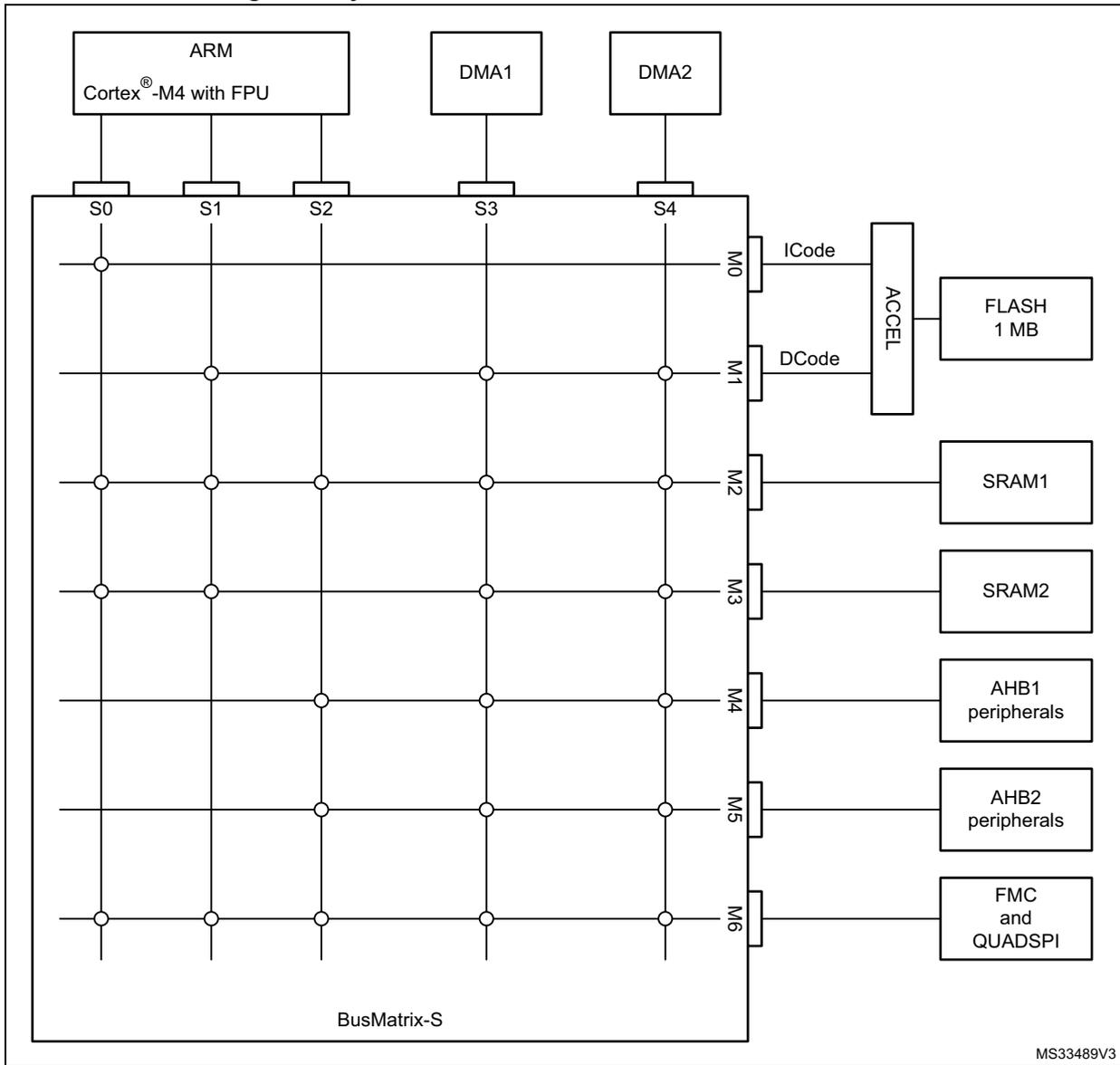
The diagram illustrates the system architecture for STM32L47x/L48x devices, centered around the BusMatrix-S . At the top, three components are connected to the matrix: ARM Cortex® -M4 with FPU (connected to S0, S1, S2), DMA1 (connected to S3), and DMA2 (connected to S4). The matrix itself is a grid with five slave ports (S0-S4) and seven master ports (M0-M6). Connections are as follows: M0 connects to ACCEL (which then connects to FLASH 1 MB ); M1 connects to ACCEL (labeled DCode ); M2 connects to SRAM1 ; M3 connects to SRAM2 ; M4 connects to AHB1 peripherals ; M5 connects to AHB2 peripherals ; and M6 connects to FMC and QUADSPI . The label BusMatrix-S is placed at the bottom of the matrix grid. A small code MS33489V3 is visible in the bottom right corner of the diagram area.
Figure 2. System architecture for STM32L49x/L4Ax
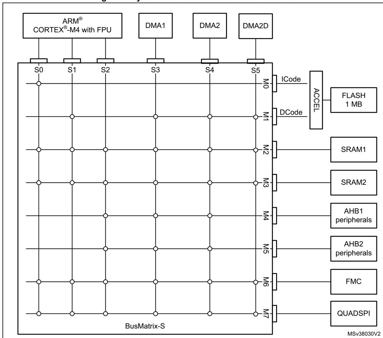
The diagram illustrates the system architecture for STM32L49x/L4Ax, centered around the BusMatrix-S. At the top, four masters are connected to the matrix: ARM® CORTEX®-M4 with FPU, DMA1, DMA2, and DMA2D. The matrix has six slave interfaces (S0 to S5) on the left and eight master interfaces (M0 to M7) on the right. The connections are as follows:
- S0 (I-bus): Connects to the ARM® CORTEX®-M4 with FPU. Targets include FLASH 1 MB (via ICode), SRAM1, SRAM2, AHB1 peripherals, AHB2 peripherals, FMC, and QUADSPI.
- S1 (D-bus): Connects to the ARM® CORTEX®-M4 with FPU. Targets include FLASH 1 MB (via DCode), SRAM1, SRAM2, AHB1 peripherals, AHB2 peripherals, FMC, and QUADSPI.
- S2 (S-bus): Connects to the ARM® CORTEX®-M4 with FPU. Targets include SRAM1, SRAM2, AHB1 peripherals, AHB2 peripherals, FMC, and QUADSPI.
- S3: Connects to DMA1. Targets include SRAM1, SRAM2, AHB1 peripherals, AHB2 peripherals, FMC, and QUADSPI.
- S4: Connects to DMA2. Targets include SRAM1, SRAM2, AHB1 peripherals, AHB2 peripherals, FMC, and QUADSPI.
- S5: Connects to DMA2D. Targets include SRAM1, SRAM2, AHB1 peripherals, AHB2 peripherals, FMC, and QUADSPI.
The matrix itself is labeled BusMatrix-S. A vertical label MSv38030V2 is present in the bottom right corner of the diagram area.
2.1.1 S0: I-bus
This bus connects the instruction bus of the Cortex®-M4 core to the BusMatrix. This bus is used by the core to fetch instructions. The targets of this bus are the internal Flash memory, SRAM1, SRAM2 and external memories through QUADSPI or the FMC.
2.1.2 S1: D-bus
This bus connects the data bus of the Cortex®-M4 core to the BusMatrix. This bus is used by the core for literal load and debug access. The targets of this bus are the internal Flash memory, SRAM1, SRAM2 and external memories through QUADSPI or the FMC.
2.1.3 S2: S-bus
This bus connects the system bus of the Cortex®-M4 core to the BusMatrix. This bus is used by the core to access data located in a peripheral or SRAM area. The targets of this
bus are the SRAM1, the AHB1 peripherals including the APB1 and APB2 peripherals, the AHB2 peripherals and the external memories through the QUADSPI or the FMC.
On STM32L49x/L4Ax devices, the SRAM2 is also accessible on this bus to allow continuous mapping with SRAM1.
2.1.4 S3, S4: DMA-bus
This bus connects the AHB master interface of the DMA to the BusMatrix. The targets of this bus are the SRAM1 and SRAM2, the AHB1 peripherals including the APB1 and APB2 peripherals, the AHB2 peripherals and the external memories through the QUADSPI or the FMC.
2.1.5 S5: DMA2D-bus (a)
This bus connects the AHB master interface of the DMA2D to the BusMatrix. The targets of this bus are the SRAM1 and SRAM2 and external memories through the QUADSPI or the FMC.
2.1.6 BusMatrix
The BusMatrix manages the access arbitration between masters. The arbitration uses a Round Robin algorithm. The BusMatrix is composed of up to six masters (CPU AHB, system bus, DCode bus, ICode bus, DMA1, DMA2 and DMA2D bus) and up to eight slaves (FLASH, SRAM1, SRAM2, AHB1 (including APB1 and APB2), AHB2, QUADSPI and FMC).
AHB/APB bridges
The two AHB/APB bridges provide full synchronous connections between the AHB and the two APB buses, allowing flexible selection of the peripheral frequency.
Refer to Section 2.2: Memory organization on page 75 for the address mapping of the peripherals connected to this bridge.
After each device reset, all peripheral clocks are disabled (except for the SRAM1/2 and Flash memory interface). Before using a peripheral you have to enable its clock in the RCC_AHBxENR and the RCC_APBxENR registers.
Note: When a 16- or 8-bit access is performed on an APB register, the access is transformed into a 32-bit access: the bridge duplicates the 16- or 8-bit data to feed the 32-bit vector.
a. it is present on L496/L4A6 only
2.2 Memory organization
2.2.1 Introduction
Program memory, data memory, registers and I/O ports are organized within the same linear 4-Gbyte address space.
The bytes are coded in memory in Little Endian format. The lowest numbered byte in a word is considered the word's least significant byte and the highest numbered byte the most significant.
The addressable memory space is divided into eight main blocks, of 512 Mbytes each.
2.2.2 Memory map and register boundary addresses
Figure 3. Memory map for STM32L47x/L48x devices
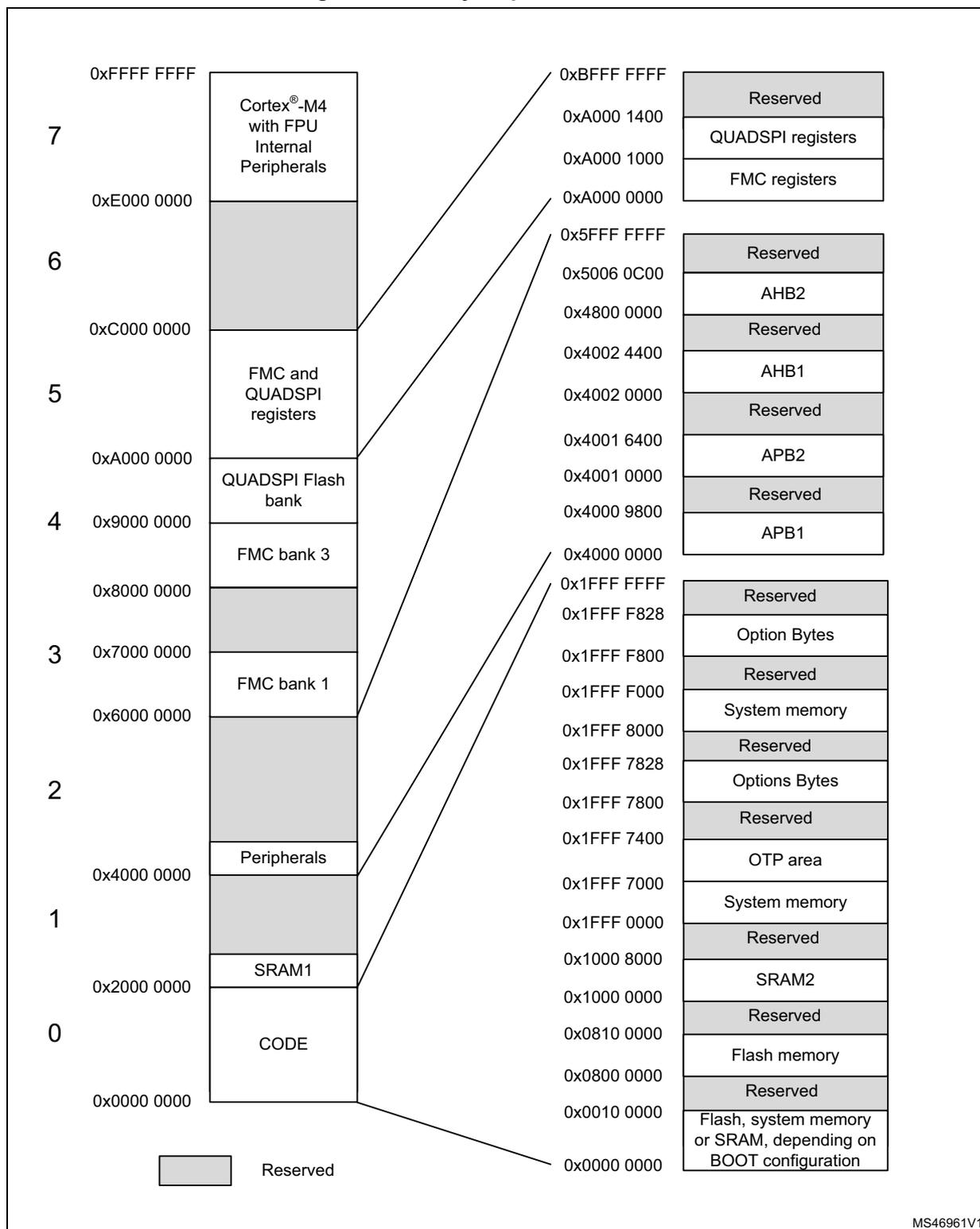
The diagram illustrates the memory map for STM32L47x/L48x devices, organized into 8 banks (0-7). The left side shows the memory bank structure with addresses, and the right side shows the corresponding register and memory content structure with addresses.
Memory Bank Structure (Left Side):
- Bank 7: 0xFFFF FFFF to 0xE000 0000. Contains Cortex®-M4 with FPU Internal Peripherals.
- Bank 6: 0xE000 0000 to 0xC000 0000. Reserved.
- Bank 5: 0xC000 0000 to 0xA000 0000. Contains FMC and QUADSPI registers.
- Bank 4: 0xA000 0000 to 0x8000 0000. Contains QUADSPI Flash bank and FMC bank 3.
- Bank 3: 0x8000 0000 to 0x6000 0000. Reserved, then FMC bank 1.
- Bank 2: 0x6000 0000 to 0x4000 0000. Reserved, then Peripherals.
- Bank 1: 0x4000 0000 to 0x2000 0000. Reserved, then SRAM1.
- Bank 0: 0x2000 0000 to 0x0000 0000. Contains CODE.
Register and Memory Content Structure (Right Side):
- 0xBFFF FFFF to 0xA000 1400: Reserved.
- 0xA000 1400 to 0xA000 1000: QUADSPI registers.
- 0xA000 1000 to 0xA000 0000: FMC registers.
- 0x5FFF FFFF to 0x5006 0C00: Reserved.
- 0x5006 0C00 to 0x4800 0000: AHB2.
- 0x4800 0000 to 0x4002 4400: Reserved.
- 0x4002 4400 to 0x4002 0000: AHB1.
- 0x4002 0000 to 0x4001 6400: Reserved.
- 0x4001 6400 to 0x4001 0000: APB2.
- 0x4001 0000 to 0x4000 9800: Reserved.
- 0x4000 9800 to 0x4000 0000: APB1.
- 0x1FFF FFFF to 0x1FFF F828: Reserved.
- 0x1FFF F828 to 0x1FFF F800: Option Bytes.
- 0x1FFF F800 to 0x1FFF F000: Reserved.
- 0x1FFF F000 to 0x1FFF 8000: System memory.
- 0x1FFF 8000 to 0x1FFF 7828: Reserved.
- 0x1FFF 7828 to 0x1FFF 7800: Options Bytes.
- 0x1FFF 7800 to 0x1FFF 7400: Reserved.
- 0x1FFF 7400 to 0x1FFF 7000: OTP area.
- 0x1FFF 7000 to 0x1FFF 0000: System memory.
- 0x1FFF 0000 to 0x1000 8000: Reserved.
- 0x1000 8000 to 0x1000 0000: SRAM2.
- 0x1000 0000 to 0x0810 0000: Reserved.
- 0x0810 0000 to 0x0800 0000: Flash memory.
- 0x0800 0000 to 0x0010 0000: Reserved.
- 0x0010 0000 to 0x0000 0000: Flash, system memory or SRAM, depending on BOOT configuration.
Legend:
- Reserved (Gray box)
MS46961V1
Figure 4. Memory map for STM32L49x/L4Ax devices
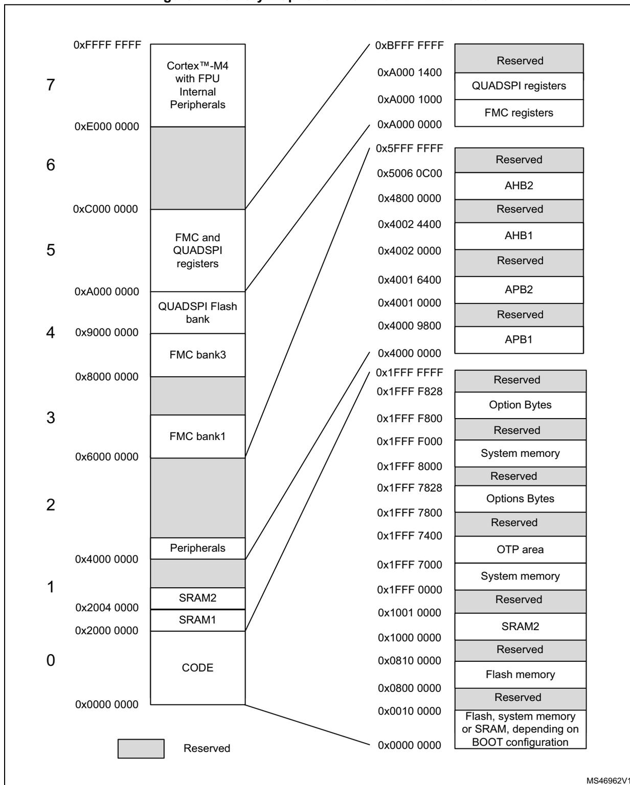
Memory map for STM32L49x/L4Ax devices
The memory map is divided into two columns. The left column shows the main memory map, and the right column shows a detailed view of the memory regions.
Left Column: Main Memory Map
| Bank | Address Range | Region |
|---|---|---|
| 7 | 0xE000 0000 - 0xFFFF FFFF | Cortex™-M4 with FPU Internal Peripherals |
| 6 | 0xC000 0000 - 0xE000 0000 | Reserved |
| 5 | 0xA000 0000 - 0xC000 0000 | FMC and QUADSPI registers |
| 4 | 0x9000 0000 - 0xA000 0000 | QUADSPI Flash bank |
| 3 | 0x8000 0000 - 0x9000 0000 | FMC bank3 |
| 2 | 0x6000 0000 - 0x8000 0000 | Reserved |
| 1 | 0x4000 0000 - 0x6000 0000 | FMC bank1 |
| 0 | 0x0000 0000 - 0x4000 0000 | Peripherals, SRAM2, SRAM1, CODE |
Right Column: Detailed Memory Regions
| Address Range | Region |
|---|---|
| 0xBFFF FFFF - 0xFFFF FFFF | Reserved |
| 0xA000 1400 - 0xA000 FFFF | QUADSPI registers |
| 0xA000 1000 - 0xA000 13FF | FMC registers |
| 0xA000 0000 - 0xA000 09FF | Reserved |
| 0x5FFF FFFF - 0xFFFF FFFF | Reserved |
| 0x5006 0C00 - 0x5FFF FFFF | Reserved |
| 0x4800 0000 - 0x5006 0BFF | AHB2 |
| 0x4002 4400 - 0x4800 0000 | Reserved |
| 0x4002 0000 - 0x4002 43FF | AHB1 |
| 0x4001 6400 - 0x4002 0000 | Reserved |
| 0x4001 0000 - 0x4001 63FF | APB2 |
| 0x4000 9800 - 0x4001 0000 | Reserved |
| 0x4000 0000 - 0x4000 97FF | APB1 |
| 0x1FFF FFFF - 0x1FFF F828 | Reserved |
| 0x1FFF F800 - 0x1FFF F827 | Option Bytes |
| 0x1FFF F000 - 0x1FFF F7FF | Reserved |
| 0x1FFF 8000 - 0x1FFF F000 | System memory |
| 0x1FFF 7828 - 0x1FFF 8000 | Reserved |
| 0x1FFF 7800 - 0x1FFF 7827 | Options Bytes |
| 0x1FFF 7400 - 0x1FFF 7800 | Reserved |
| 0x1FFF 7000 - 0x1FFF 73FF | OTP area |
| 0x1FFF 0000 - 0x1FFF 7000 | System memory |
| 0x1001 0000 - 0x1FFF 0000 | Reserved |
| 0x1000 0000 - 0x1001 0000 | SRAM2 |
| 0x0810 0000 - 0x1000 0000 | Reserved |
| 0x0800 0000 - 0x0810 0000 | Flash memory |
| 0x0010 0000 - 0x0800 0000 | Reserved |
| 0x0000 0000 - 0x0010 0000 | Flash, system memory or SRAM, depending on BOOT configuration |
Legend: Reserved
MS46962V1
It is forbidden to access QUADSPI Flash bank area before having properly configured and enabled the QUADSPI peripheral.
All the memory map areas that are not allocated to on-chip memories and peripherals are considered “Reserved”. For the detailed mapping of available memory and register areas, refer to the following table.
The following table gives the boundary addresses of the peripherals available in the devices.
Table 1. STM32L47x/L48x devices memory map and peripheral register boundary addresses (1)
| Bus | Boundary address | Size (bytes) | Peripheral | Peripheral register map |
|---|---|---|---|---|
| AHB2 | 0x5006 0800 - 0x5006 0BFF | 1 KB | RNG | Section 27.7.4: RNG register map |
| 0x5006 0400 - 0x5006 07FF | 1 KB | Reserved | - | |
| 0x5006 0000 - 0x5006 03FF | 1 KB | AES (2) | Section 28.7.18: AES register map | |
| 0x5004 0400 - 0x5005 FFFF | 127 KB | Reserved | - | |
| 0x5004 0000 - 0x5004 03FF | 1 KB | ADC | Section 18.9: ADC register map | |
| 0x5000 0000 - 0x5003 FFFF | 256 KB | OTG_FS (3) | Section 47.15.57: OTG_FS register map | |
| 0x4800 2000 - 0x4FFF FFFF | ~127 MB | Reserved | - | |
| 0x4800 1C00 - 0x4800 1FFF | 1 KB | GPIOH | Section 8.5.13: GPIO register map | |
| 0x4800 1800 - 0x4800 1BFF | 1 KB | GPIOG | Section 8.5.13: GPIO register map | |
| 0x4800 1400 - 0x4800 17FF | 1 KB | GPIOF | Section 8.5.13: GPIO register map | |
| 0x4800 1000 - 0x4800 13FF | 1 KB | GPIOE | Section 8.5.13: GPIO register map | |
| 0x4800 0C00 - 0x4800 0FFF | 1 KB | GPIO D | Section 8.5.13: GPIO register map | |
| 0x4800 0800 - 0x4800 0BFF | 1 KB | GPIOC | Section 8.5.13: GPIO register map | |
| 0x4800 0400 - 0x4800 07FF | 1 KB | GPIOB | Section 8.5.13: GPIO register map | |
| 0x4800 0000 - 0x4800 03FF | 1 KB | GPIOA | Section 8.5.13: GPIO register map | |
| 0x4002 4400 - 0x47FF FFFF | ~127 MB | Reserved | - |
Table 1. STM32L47x/L48x devices memory map and peripheral register boundary addresses (1) (continued)
| Bus | Boundary address | Size (bytes) | Peripheral | Peripheral register map |
|---|---|---|---|---|
| AHB1 | 0x4002 4000 - 0x4002 43FF | 1 KB | TSC | Section 26.6.11: TSC register map |
| 0x4002 3400 - 0x4002 3FFF | 3 KB | Reserved | - | |
| 0x4002 3000 - 0x4002 33FF | 1 KB | CRC | Section 15.4.6: CRC register map | |
| 0x4002 2400 - 0x4002 2FFF | 3 KB | Reserved | - | |
| 0x4002 2000 - 0x4002 23FF | 1 KB | FLASH registers | Section 3.7.17: FLASH register map | |
| 0x4002 1400 - 0x4002 1FFF | 3 KB | Reserved | - | |
| 0x4002 1000 - 0x4002 13FF | 1 KB | RCC | Section 6.4.33: RCC register map | |
| 0x4002 0800 - 0x4002 0FFF | 2 KB | Reserved | - | |
| 0x4002 0400 - 0x4002 07FF | 1 KB | DMA2 | Section 11.6.8: DMA register map | |
| 0x4002 0000 - 0x4002 03FF | 1 KB | DMA1 | Section 11.6.8: DMA register map | |
| APB2 | 0x4001 6400 - 0x4001 FFFF | 39 KB | Reserved | - |
| 0x4001 6000 - 0x4001 63FF | 1 KB | DFSDM1 | Section 24.8.16: DFSDM register map | |
| 0x4001 5C00 - 0x4001 5FFF | 1 KB | Reserved | - | |
| 0x4001 5800 - 0x4001 5BFF | 1 KB | SAI2 | Section 43.5.18: SAI register map | |
| 0x4001 5400 - 0x4001 57FF | 1 KB | SAI1 | Section 43.5.18: SAI register map | |
| 0x4001 4C00 - 0x4001 53FF | 2 KB | Reserved | - |
Table 1. STM32L47x/L48x devices memory map and peripheral register boundary addresses (1) (continued)
| Bus | Boundary address | Size (bytes) | Peripheral | Peripheral register map |
|---|---|---|---|---|
| APB2 | 0x4001 4800 - 0x4001 4BFF | 1 KB | TIM17 | Section 32.7.21: TIM16/TIM17 register map |
| 0x4001 4400 - 0x4001 47FF | 1 KB | TIM16 | Section 32.7.21: TIM16/TIM17 register map | |
| 0x4001 4000 - 0x4001 43FF | 1 KB | TIM15 | Section 32.7.21: TIM16/TIM17 register map | |
| 0x4001 3C00 - 0x4001 3FFF | 1 KB | Reserved | - | |
| 0x4001 3800 - 0x4001 3BFF | 1 KB | USART1 | Section 40.8.12: USART register map | |
| 0x4001 3400 - 0x4001 37FF | 1 KB | TIM8 | Section 30.4.33: TIM8 register map | |
| 0x4001 3000 - 0x4001 33FF | 1 KB | SPI1 | Section 42.6.8: SPI register map | |
| 0x4001 2C00 - 0x4001 2FFF | 1 KB | TIM1 | Section 30.4.32: TIM1 register map | |
| 0x4001 2800 - 0x4001 2BFF | 1 KB | SDMMC1 | Section 45.8.16: SDMMC register map | |
| 0x4001 2000 - 0x4001 27FF | 2 KB | Reserved | - | |
| 0x4001 1C00 - 0x4001 1FFF | 1 KB | FIREWALL | Section 4.4.8: Firewall register map | |
| 0x4001 0800 - 0x4001 1BFF | 5 KB | Reserved | - | |
| 0x4001 0400 - 0x4001 07FF | 1 KB | EXTI | Section 14.5.13: EXTI register map | |
| 0x4001 0200 - 0x4001 03FF | 1 KB | COMP | Section 22.6.3: COMP register map | |
| 0x4001 0030 - 0x4001 01FF | VREFBUF | Section 21.4.3: VREFBUF register map | ||
| 0x4001 0000 - 0x4001 002F | SYSCFG | Section 9.2.12: SYSCFG register map |
Table 1. STM32L47x/L48x devices memory map and peripheral register boundary addresses (1) (continued)
| Bus | Boundary address | Size (bytes) | Peripheral | Peripheral register map |
|---|---|---|---|---|
| APB1 | 0x4000 9800 - 0x4000 FFFF | 26 KB | Reserved | - |
| 0x4000 9400 - 0x4000 97FF | 1 KB | LPTIM2 | Section 34.7.11: LPTIM register map | |
| 0x4000 8C00 - 0x4000 93FF | 2 KB | Reserved | - | |
| 0x4000 8800 - 0x4000 8BFF | 1 KB | SWPMI1 | Section 44.6.10: SWPMI register map and reset value table | |
| 0x4000 8400 - 0x4000 87FF | 1 KB | Reserved | - | |
| 0x4000 8000 - 0x4000 83FF | 1 KB | LPUART1 | Section 41.7.10: LPUART register map | |
| 0x4000 7C00 - 0x4000 7FFF | 1 KB | LPTIM1 | Section 34.7.11: LPTIM register map | |
| 0x4000 7800 - 0x4000 7BFF | 1 KB | OPAMP | Section 23.5.7: OPAMP register map | |
| 0x4000 7400 - 0x4000 77FF | 1 KB | DAC1 | Section 19.7.21: DAC register map | |
| 0x4000 7000 - 0x4000 73FF | 1 KB | PWR | Section 5.4.26: PWR register map and reset value table | |
| 0x4000 6800 - 0x4000 6FFF | 2 KB | Reserved | - | |
| 0x4000 6400 - 0x4000 67FF | 1 KB | CAN1 | Section 46.9.5: bxCAN register map | |
| 0x4000 6000 - 0x4000 63FF | 1 KB | Reserved | - | |
| 0x4000 5C00 - 0x4000 5FFF | 1 KB | I2C3 | Section 39.9.12: I2C register map | |
| 0x4000 5800 - 0x4000 5BFF | 1 KB | I2C2 | Section 39.9.12: I2C register map | |
| 0x4000 5400 - 0x4000 57FF | 1 KB | I2C1 | Section 39.9.12: I2C register map |
Table 1. STM32L47x/L48x devices memory map and peripheral register boundary addresses (1) (continued)
| Bus | Boundary address | Size (bytes) | Peripheral | Peripheral register map |
|---|---|---|---|---|
| APB1 | 0x4000 5000 - 0x4000 53FF | 1 KB | UART5 | Section 40.8.12: USART register map |
| 0x4000 4C00 - 0x4000 4FFF | 1 KB | UART4 | Section 40.8.12: USART register map | |
| 0x4000 4800 - 0x4000 4BFF | 1 KB | USART3 | Section 40.8.12: USART register map | |
| 0x4000 4400 - 0x4000 47FF | 1 KB | USART2 | Section 40.8.12: USART register map | |
| 0x4000 4000 - 0x4000 43FF | 1 KB | Reserved | - | |
| 0x4000 3C00 - 0x4000 3FFF | 1 KB | SPI3 | Section 42.6.8: SPI register map | |
| 0x4000 3800 - 0x4000 3BFF | 1 KB | SPI2 | Section 42.6.8: SPI register map | |
| 0x4000 3400 - 0x4000 37FF | 1 KB | Reserved | - | |
| 0x4000 3000 - 0x4000 33FF | 1 KB | IWDG | Section 36.4.6: IWDG register map | |
| 0x4000 2C00 - 0x4000 2FFF | 1 KB | WWDG | Section 37.5.4: WWDG register map | |
| 0x4000 2800 - 0x4000 2BFF | 1 KB | RTC | Section 38.6.21: RTC register map | |
| 0x4000 2400 - 0x4000 27FF | 1 KB | LCD (4) | Section 25.6.8: LCD register map | |
| 0x4000 1800 - 0x4000 2400 | 3 KB | Reserved | - | |
| 0x4000 1400 - 0x4000 17FF | 1 KB | TIM7 | Section 33.4.9: TIMx register map | |
| 0x4000 1000 - 0x4000 13FF | 1 KB | TIM6 | Section 33.4.9: TIMx register map | |
| 0x4000 0C00 - 0x4000 0FFF | 1 KB | TIM5 | Section 31.4.26: TIMx register map | |
| 0x4000 0800 - 0x4000 0BFF | 1 KB | TIM4 | Section 31.4.26: TIMx register map | |
| 0x4000 0400 - 0x4000 07FF | 1 KB | TIM3 | Section 31.4.26: TIMx register map | |
| 0x4000 0000 - 0x4000 03FF | 1 KB | TIM2 | Section 31.4.26: TIMx register map |
1. The gray color is used for reserved boundary addresses.
2. Available on STM32L48x devices only.
3. Available on STM32L4x5/L4x6 devices only.
4. Available on STM32L4x6 devices only.
Table 2. STM32L49x/L4Ax devices memory map and peripheral register boundary addresses (1)
| Bus | Boundary address | Size (bytes) | Peripheral | Peripheral register map |
|---|---|---|---|---|
| AHB4 | 0xA000 1000 - 0xA000 13FF | 1 KB | QUADSPI | Section 17.6.14: QUADSPI register map |
| AHB3 | 0xA000 0400 - 0xA000 0FFF | 3 KB | Reserved | - |
| 0xA000 0000 - 0xA000 03FF | 1 KB | FMC | Section 16.7.8: FMC register map | |
| - | 0x5006 0C00 - 0x5FFF FFFF | ~260 MB | Reserved | - |
| AHB2 | 0x5006 0800 - 0x5006 0BFF | 1 KB | RNG | Section 27.7.4: RNG register map |
| 0x5006 0400 - 0x5006 07FF | 1 KB | HASH | Section 29.7.8: HASH register map | |
| 0x5006 0000 - 0x5006 03FF | 1 KB | AES (2) | Section 28.7.18: AES register map | |
| 0x5005 0400 - 0x5005 FFFF | 63 KB | Reserved | - | |
| 0x5005 0000 - 0x5005 03FF | 1 KB | DCMI | Section 20.5.12: DCMI register map | |
| 0x5004 0400 - 0x5004 FFFF | 63 KB | Reserved | - | |
| 0x5004 0000 - 0x5004 03FF | 1 KB | ADC | Section 18.9: ADC register map | |
| 0x5000 0000 - 0x5003 FFFF | 256 KB | OTG_FS | Section 47.15.57: OTG_FS register map | |
| 0x4800 2400 - 0x4FFF FFFF | ~127 MB | Reserved | - | |
| 0x4800 2000 - 0x4800 23FF | 1 KB | GPIOI | Section 8.5.13: GPIO register map | |
| 0x4800 1C00 - 0x4800 1FFF | 1 KB | GPIOH | Section 8.5.13: GPIO register map | |
| 0x4800 1800 - 0x4800 1BFF | 1 KB | GPIOG | Section 8.5.13: GPIO register map | |
| 0x4800 1400 - 0x4800 17FF | 1 KB | GPIOF | Section 8.5.13: GPIO register map | |
| 0x4800 1000 - 0x4800 13FF | 1 KB | GPIOE | Section 8.5.13: GPIO register map | |
| 0x4800 0C00 - 0x4800 0FFF | 1 KB | GPIO_D | Section 8.5.13: GPIO register map | |
| 0x4800 0800 - 0x4800 0BFF | 1 KB | GPIOC | Section 8.5.13: GPIO register map | |
| 0x4800 0400 - 0x4800 07FF | 1 KB | GPIOB | Section 8.5.13: GPIO register map | |
| 0x4800 0000 - 0x4800 03FF | 1 KB | GPIOA | Section 8.5.13: GPIO register map | |
| - | 0x4002 BC00 - 0x47FF FFFF | ~127 MB | Reserved | - |
Table 2. STM32L49x/L4Ax devices memory map and peripheral register boundary addresses (1) (continued)
| Bus | Boundary address | Size (bytes) | Peripheral | Peripheral register map |
|---|---|---|---|---|
| AHB1 | 0x4002 B000 - 0x4002 BBFF | 3 KB | DMA2D | Section 12.5.26: DMA2D register map |
| 0x4002 4400 - 0x4002 AFFF | 27 KB | Reserved | - | |
| 0x4002 4000 - 0x4002 43FF | 1 KB | TSC | Section 26.6.11: TSC register map | |
| 0x4002 3400 - 0x4002 3FFF | 1 KB | Reserved | - | |
| 0x4002 3000 - 0x4002 33FF | 1 KB | CRC | Section 15.4.6: CRC register map | |
| 0x4002 2400 - 0x4002 2FFF | 3 KB | Reserved | - | |
| 0x4002 2000 - 0x4002 23FF | 1 KB | FLASH registers | Section 3.7.17: FLASH register map | |
| 0x4002 1400 - 0x4002 1FFF | 3 KB | Reserved | - | |
| 0x4002 1000 - 0x4002 13FF | 1 KB | RCC | Section 6.4.33: RCC register map | |
| 0x4002 0800 - 0x4002 0FFF | 2 KB | Reserved | - | |
| 0x4002 0400 - 0x4002 07FF | 1 KB | DMA2 | Section 11.6.8: DMA register map | |
| 0x4002 0000 - 0x4002 03FF | 1 KB | DMA1 | Section 11.6.8: DMA register map | |
| APB2 | 0x4001 6400 - 0x4001 FFFF | 39 KB | Reserved | - |
| 0x4001 6000 - 0x4001 63FF | 1 KB | DFSDM1 | Section 24.8.16: DFSDM register map | |
| 0x4001 5C00 - 0x4001 5FFF | 1 KB | Reserved | - | |
| 0x4001 5800 - 0x4001 5BFF | 1 KB | SAI2 | Section 43.5: SAI registers | |
| 0x4001 5400 - 0x4001 57FF | 1 KB | SAI1 | Section 43.5: SAI registers | |
| 0x4001 4C00 - 0x4001 53FF | 2 KB | Reserved | - | |
| 0x4001 4800 - 0x4001 4BFF | 1 KB | TIM17 | Section 32.7.21: TIM16/TIM17 register map | |
| 0x4001 4400 - 0x4001 47FF | 1 KB | TIM16 | Section 32.7.21: TIM16/TIM17 register map | |
| 0x4001 4000 - 0x4001 43FF | 1 KB | TIM15 | Section 32.6.21: TIM15 register map | |
| 0x4001 3C00 - 0x4001 3FFF | 1 KB | Reserved | - | |
| 0x4001 3800 - 0x4001 3BFF | 1 KB | USART1 | Section 40.8.12: USART register map | |
| 0x4001 3400 - 0x4001 37FF | 1 KB | TIM8 | Section 30.4.33: TIM8 register map | |
| 0x4001 3000 - 0x4001 33FF | 1 KB | SPI1 | Section 42.6.8: SPI register map | |
| 0x4001 2C00 - 0x4001 2FFF | 1 KB | TIM1 | Section 30.4.32: TIM1 register map | |
| 0x4001 2800 - 0x4001 2BFF | 1 KB | SDMMC1 | Section 45.8.16: SDMMC register map | |
| 0x4001 2000 - 0x4001 27FF | 2 KB | Reserved | - | |
| 0x4001 1C00 - 0x4001 1FFF | 1 KB | FIREWALL | Section 4.4.8: Firewall register map | |
| 0x4001 0800 - 0x4001 1BFF | 5 KB | Reserved | - | |
| 0x4001 0400 - 0x4001 07FF | 1 KB | EXTI | Section 14.5.13: EXTI register map |
Table 2. STM32L49x/L4Ax devices memory map and peripheral register boundary addresses (1) (continued)
| Bus | Boundary address | Size (bytes) | Peripheral | Peripheral register map |
|---|---|---|---|---|
| APB2 | 0x4001 0200 - 0x4001 03FF | 1 KB | COMP | Section 22.6.3: COMP register map |
| 0x4001 0030 - 0x4001 01FF | VREFBUF | Section 21.4.3: VREFBUF register map | ||
| 0x4001 0000 - 0x4001 002F | SYSCFG | Section 9.2.12: SYSCFG register map | ||
| APB1 | 0x4000 9800 - 0x4000 FFFF | 26 KB | Reserved | - |
| 0x4000 9400 - 0x4000 97FF | 1 KB | LPTIM2 | Section 34.7.11: LPTIM register map | |
| 0x4000 8C00 - 0x4000 93FF | 2 KB | Reserved | - | |
| 0x4000 8800 - 0x4000 8BFF | 1 KB | SWPMI1 | Section 44.6.10: SWPMI register map and reset value table | |
| 0x4000 8400 - 0x4000 87FF | 1 KB | I2C4 | Section 39.9.12: I2C register map | |
| 0x4000 8000 - 0x4000 83FF | 1 KB | LPUART1 | Section 41.7.10: LPUART register map | |
| 0x4000 7C00 - 0x4000 7FFF | 1 KB | LPTIM1 | Section 34.7.11: LPTIM register map | |
| 0x4000 7800 - 0x4000 7BFF | 1 KB | OPAMP | Section 23.5.7: OPAMP register map | |
| 0x4000 7400 - 0x4000 77FF | 1 KB | DAC1 | Section 19.7.21: DAC register map | |
| 0x4000 7000 - 0x4000 73FF | 1 KB | PWR | Section 5.4.26: PWR register map and reset value table | |
| 0x4000 6C00 - 0x4000 6FFF | 1 KB | Reserved | - | |
| 0x4000 6800 - 0x4000 6BFF | 1 KB | CAN2 | Section 46.9.5: bxCAN register map | |
| 0x4000 6400 - 0x4000 67FF | 1 KB | CAN1 | Section 46.9.5: bxCAN register map | |
| 0x4000 6000 - 0x4000 63FF | 1 KB | CRS | Section 7.7.5: CRS register map | |
| 0x4000 5C00 - 0x4000 5FFF | 1 KB | I2C3 | Section 39.9.12: I2C register map | |
| 0x4000 5800 - 0x4000 5BFF | 1 KB | I2C2 | Section 39.9.12: I2C register map | |
| 0x4000 5400 - 0x4000 57FF | 1 KB | I2C1 | Section 39.9.12: I2C register map | |
| 0x4000 5000 - 0x4000 53FF | 1 KB | UART5 | Section 40.8.12: USART register map | |
| 0x4000 4C00 - 0x4000 4FFF | 1 KB | UART4 | Section 40.8.12: USART register map |
Table 2. STM32L49x/L4Ax devices memory map and peripheral register boundary addresses (1) (continued)
| Bus | Boundary address | Size (bytes) | Peripheral | Peripheral register map |
|---|---|---|---|---|
| APB1 | 0x4000 4800 - 0x4000 4BFF | 1 KB | USART3 | Section 40.8.12: USART register map |
| 0x4000 4400 - 0x4000 47FF | 1 KB | USART2 | Section 40.8.12: USART register map | |
| 0x4000 4000 - 0x4000 43FF | 1 KB | Reserved | - | |
| 0x4000 3C00 - 0x4000 3FFF | 1 KB | SPI3 | Section 42.6.8: SPI register map | |
| 0x4000 3800 - 0x4000 3BFF | 1 KB | SPI2 | Section 42.6.8: SPI register map | |
| 0x4000 3400 - 0x4000 37FF | 1 KB | Reserved | - | |
| 0x4000 3000 - 0x4000 33FF | 1 KB | IWDG | Section 36.4.6: IWDG register map | |
| 0x4000 2C00 - 0x4000 2FFF | 1 KB | WWDG | Section 37.5.4: WWDG register map | |
| 0x4000 2800 - 0x4000 2BFF | 1 KB | RTC | Section 38.6.21: RTC register map | |
| 0x4000 2400 - 0x4000 27FF | 1 KB | LCD | Section 25.6.8: LCD register map | |
| 0x4000 1800 - 0x4000 23FF | 3 KB | Reserved | - | |
| 0x4000 1400 - 0x4000 17FF | 1 KB | TIM7 | Section 33.4.9: TIMx register map | |
| 0x4000 1000 - 0x4000 13FF | 1 KB | TIM6 | Section 33.4.9: TIMx register map | |
| 0x4000 0C00 - 0x4000 0FFF | 1 KB | TIM5 | Section 31.4.26: TIMx register map | |
| 0x4000 0800 - 0x4000 0BFF | 1 KB | TIM4 | Section 31.4.26: TIMx register map | |
| 0x4000 0400 - 0x4000 07FF | 1 KB | TIM3 | Section 31.4.26: TIMx register map | |
| 0x4000 0000 - 0x4000 03FF | 1 KB | TIM2 | Section 31.4.26: TIMx register map |
1. The gray color is used for reserved boundary addresses.
2. Available on STM32L4Ax only.
2.3 Bit banding
The Cortex ® -M4 memory map includes two bit-band regions. These regions map each word in an alias region of memory to a bit in a bit-band region of memory. Writing to a word in the alias region has the same effect as a read-modify-write operation on the targeted bit in the bit-band region.
In the STM32L4x6 devices both the peripheral registers and the SRAM1 are mapped to a bit-band region, so that single bit-band write and read operations are allowed. The operations are only available for Cortex ® -M4 accesses, and not from other bus masters (e.g. DMA).
A mapping formula shows how to reference each word in the alias region to a corresponding bit in the bit-band region. The mapping formula is:
where:
- – bit_word_addr is the address of the word in the alias memory region that maps to the targeted bit
- – bit_band_base is the starting address of the alias region
- – byte_offset is the number of the byte in the bit-band region that contains the targeted bit
- – bit_number is the bit position (0-7) of the targeted bit
Example
The following example shows how to map bit 2 of the byte located at SRAM1 address 0x20000300 to the alias region:
Writing to address 0x22006008 has the same effect as a read-modify-write operation on bit 2 of the byte at SRAM1 address 0x20000300.
Reading address 0x22006008 returns the value (0x01 or 0x00) of bit 2 of the byte at SRAM1 address 0x20000300 (0x01: bit set; 0x00: bit reset).
For more information on bit-banding, refer to the Cortex®-M4 programming manual (see Related documents on page 1 ).
2.4 Embedded SRAM
The STM32L47x/L48x/L49x/L4Ax devices feature up to 320 Kbytes SRAM:
- • 96 Kbytes SRAM1 and 32 Kbyte SRAM2 on STM32L47x/L48x.
- • 256 Kbyte SRAM1 and 64 Kbyte SRAM2 on STM32L49x/L4Ax devices.
These SRAM can be accessed as bytes, half-words (16 bits) or full words (32 bits). These memories can be addressed at maximum system clock frequency without wait state and thus by both CPU and DMA.
The CPU can access the SRAM1 through the system bus or through the ICode/DCode buses when boot from SRAM1 is selected or when physical remap is selected ( Section 9.2.1: SYSCFG memory remap register (SYSCFG_MEMRMP) in the SYSCFG controller). To get the maximum performance on SRAM1 execution, physical remap should be selected (boot or software selection).
Execution can be performed from SRAM2 with maximum performance without any remap thanks to access through ICode bus.
On STM32L49x/L4Ax devices, the SRAM2 is aliased at address 0x2004 0000, offering a continuous address space with the SRAM1.
2.4.1 SRAM2 parity check
The user can enable the SRAM2 parity check using the option bit SRAM2_PE in the user option byte (refer to Section 3.4.1: Option bytes description ).
The data bus width is 36 bits because 4 bits are available for parity check (1 bit per byte) in order to increase memory robustness, as required for instance by Class B or SIL norms.
The parity bits are computed and stored when writing into the SRAM2. Then, they are automatically checked when reading. If one bit fails, an NMI is generated. The same error can also be linked to the BRK_IN Break input of TIM1/TIM8/TIM15/TIM16/TIM17, with the SPL control bit in the SYSCFG configuration register 2 (SYSCFG_CFGR2) . The SRAM2 Parity Error flag (SPF) is available in the SYSCFG configuration register 2 (SYSCFG_CFGR2) .
Note: When enabling the RAM parity check, it is advised to initialize by software the whole RAM memory at the beginning of the code, to avoid getting parity errors when reading non-initialized locations.
2.4.2 SRAM2 Write protection
The SRAM2 can be write protected with a page granularity of 1 Kbyte.
Table 3. SRAM2 organization
| Page number | Start address | End address |
|---|---|---|
| Page 0 | 0x1000 0000 | 0x1000 03FF |
| Page 1 | 0x1000 0400 | 0x1000 07FF |
| Page 2 | 0x1000 0800 | 0x1000 0BFF |
| Page 3 | 0x1000 0C00 | 0x1000 0FFF |
| Page 4 | 0x1000 1000 | 0x1000 13FF |
| Page 5 | 0x1000 1400 | 0x1000 17FF |
| Page 6 | 0x1000 1800 | 0x1000 1BFF |
| Page 7 | 0x1000 1C00 | 0x1000 1FFF |
| Page 8 | 0x1000 2000 | 0x1000 23FF |
| Page 9 | 0x1000 2400 | 0x1000 27FF |
| Page 10 | 0x1000 2800 | 0x1000 2BFF |
| Page 11 | 0x1000 2C00 | 0x1000 2FFF |
| Page 12 | 0x1000 3000 | 0x1000 33FF |
| Page 13 | 0x1000 3400 | 0x1000 37FF |
| Page 14 | 0x1000 3800 | 0x1000 3BFF |
| Page 15 | 0x1000 3C00 | 0x1000 3FFF |
| Page 16 | 0x1000 4000 | 0x1000 43FF |
| Page 17 | 0x1000 4400 | 0x1000 47FF |
| Page 18 | 0x1000 4800 | 0x1000 4BFF |
| Page 19 | 0x1000 4C00 | 0x1000 4FFF |
| Page 20 | 0x1000 5000 | 0x1000 53FF |
| Page 21 | 0x1000 5400 | 0x1000 57FF |
| Page 22 | 0x1000 5800 | 0x1000 5BFF |
Table 3. SRAM2 organization (continued)
| Page number | Start address | End address |
|---|---|---|
| Page 23 | 0x1000 5C00 | 0x1000 5FFF |
| Page 24 | 0x1000 6000 | 0x1000 63FF |
| Page 25 | 0x1000 6400 | 0x1000 67FF |
| Page 26 | 0x1000 6800 | 0x1000 6BFF |
| Page 27 | 0x1000 6C00 | 0x1000 6FFF |
| Page 28 | 0x1000 7000 | 0x1000 73FF |
| Page 29 | 0x1000 7400 | 0x1000 77FF |
| Page 30 | 0x1000 7800 | 0x1000 7BFF |
| Page 31 | 0x1000 7C00 | 0x1000 7FFF |
| STM32L49x/L4Ax devices only | ||
| Page 32 | 0x1000 8000 | 0x1000 83FF |
| Page 33 | 0x1000 8400 | 0x1000 87FF |
| Page 34 | 0x1000 8800 | 0x1000 8BFF |
| Page 35 | 0x1000 8C00 | 0x1000 8FFF |
| Page 36 | 0x1000 9000 | 0x1000 93FF |
| Page 37 | 0x1000 9400 | 0x1000 97FF |
| Page 38 | 0x1000 9800 | 0x1000 9BFF |
| Page 39 | 0x1000 9C00 | 0x1000 9FFF |
| Page 40 | 0x1000 A000 | 0x1000 A3FF |
| Page 41 | 0x1000 A400 | 0x1000 A7FF |
| Page 42 | 0x1000 A800 | 0x1000 ABFF |
| Page 43 | 0x1000 AC00 | 0x1000 AFFF |
| Page 44 | 0x1000 B000 | 0x1000 B3FF |
| Page 45 | 0x1000 B400 | 0x1000 B7FF |
| Page 46 | 0x1000 B800 | 0x1000 BBFF |
| Page 47 | 0x1000 BC00 | 0x1000 BFFF |
| Page 48 | 0x1000 C000 | 0x1000 C3FF |
| Page 49 | 0x1000 C400 | 0x1000 C7FF |
| Page 50 | 0x1000 C800 | 0x1000 CBFF |
| Page 51 | 0x1000 CC00 | 0x1000 CFFF |
| Page 52 | 0x1000 D000 | 0x1000 D3FF |
| Page 53 | 0x1000 D400 | 0x1000 D7FF |
| Page 54 | 0x1000 D800 | 0x1000 DBFF |
| Page 55 | 0x1000 DC00 | 0x1000 DFFF |
| Page 56 | 0x1000 E000 | 0x1000 E3FF |
| Page number | Start address | End address |
|---|---|---|
| Page 57 | 0x1000 E400 | 0x1000 E7FF |
| Page 58 | 0x1000 E800 | 0x1000 EBFF |
| Page 59 | 0x1000 EC00 | 0x1000 EFFF |
| Page 60 | 0x1000 F000 | 0x1000 F3FF |
| Page 61 | 0x1000 F400 | 0x1000 F7FF |
| Page 62 | 0x1000 F800 | 0x1000 FBFF |
| Page 63 | 0x1000 FC00 | 0x1000 FFFF |
The write protection can be enabled in SYSCFG SRAM2 write protection register (SYSCFG_SWPR) in the SYSCFG block. This is a register with write '1' once mechanism, which means by writing '1' on a bit it will setup the write protection for that page of SRAM and it can be removed/cleared by a system reset only.
2.4.3 SRAM2 Read protection
The SRAM2 is protected with the Read protection (RDP). Refer to Section 3.5.1: Read protection (RDP) for more details.
2.4.4 SRAM2 Erase
The SRAM2 can be erased with a system reset using the option bit SRAM2_RST in the user option byte (refer to Section 3.4.1: Option bytes description ).
The SRAM2 erase can also be requested by software by setting the bit SRAM2ER in the SYSCFG SRAM2 control and status register (SYSCFG_SCSR) .
2.5 Flash memory overview
The Flash memory is composed of two distinct physical areas:
- • The main Flash memory block. It contains the application program and user data if necessary.
- • The information block. It is composed of three parts:
- – Option bytes for hardware and memory protection user configuration.
- – System memory that contains the ST proprietary code.
- – OTP (one-time programmable) area
The Flash interface implements instruction access and data access based on the AHB protocol. It also implements the logic necessary to carry out the Flash memory operations (program/erase) controlled through the Flash registers Refer to Section 3: Embedded Flash memory (FLASH) for more details.
2.6 Boot configuration
2.6.1 Boot configuration for STM32L47x/L48x devices
In the STM32L47x/L48x devices, three different boot modes can be selected through the BOOT0 pin and nBOOT1 bit in the User option byte, as shown in the following table.
Table 4. Boot modes
| Boot mode selection | Boot mode | Aliasings | |
|---|---|---|---|
| BOOT1 (1) | BOOT0 | ||
| x | 0 | Main Flash memory | Main Flash memory is selected as boot area |
| 0 | 1 | System memory | System memory is selected as boot area |
| 1 | 1 | Embedded SRAM1 | Embedded SRAM1 is selected as boot area |
1. The BOOT1 value is the opposite of the nBOOT1 Option Bit.
The values on both BOOT0 pin and nBOOT1 bit are latched after a reset. It is up to the user to set nBOOT1 and BOOT0 to select the required boot mode.
The BOOT0 pin and nBOOT1 bit are also re-sampled when exiting from Standby mode. Consequently they must be kept in the required Boot mode configuration in Standby mode. After this startup delay has elapsed, the CPU fetches the top-of-stack value from address 0x0000 0000, then starts code execution from the boot memory at 0x0000 0004.
Depending on the selected boot mode, main Flash memory, system memory or SRAM1 is accessible as follows:
- • Boot from main Flash memory: the main Flash memory is aliased in the boot memory space (0x0000 0000), but still accessible from its original memory space (0x0800 0000). In other words, the Flash memory contents can be accessed starting from address 0x0000 0000 or 0x0800 0000.
- • Boot from system memory: the system memory is aliased in the boot memory space (0x0000 0000), but still accessible from its original memory space (0x1FFF 0000).
- • Boot from the embedded SRAM1: the SRAM1 is aliased in the boot memory space (0x0000 0000), but it is still accessible from its original memory space (0x2000 0000).
Note: When the device boots from SRAM, in the application initialization code, you have to relocate the vector table in SRAM using the NVIC exception table and the offset register.
When booting from the main Flash memory, the application software can either boot from bank 1 or from bank 2. By default, boot from bank 1 is selected.
To select boot from Flash memory bank 2, set the BFB2 bit in the user option bytes. When this bit is set and the boot pins are in the “boot from main Flash memory” configuration, the device boots from system memory, and the boot loader jumps to execute the user application programmed in Flash memory bank 2. The system memory remains aliased to the boot memory space (0x0000 0000). For further details, please refer to AN2606.
Note: When booting from bank 2, the boot loader will swap the Flash memory banks. Consequently, in the application initialization code, you have to relocate the vector table to bank 2 swapped base address (0x0800 0000) using the NVIC exception table and offset register.
Physical remap
Once the boot pins are selected, the application software can modify the memory accessible in the code area (in this way the code can be executed through the ICode bus in place of the System bus). This modification is performed by programming the SYSCFG memory remap register (SYSCFG_MEMRMP) in the SYSCFG controller.
The following memories can thus be remapped:
- • Main Flash memory
- • System memory
- • Embedded SRAM1 (96 KB)
- • FSMC bank 1 (NOR/PSRAM 1 and 2)
- • Quad-SPI memory
Table 5. Memory mapping versus boot mode/physical remap
| Addresses | Boot/remap in main Flash memory | Boot/remap in embedded SRAM 1 | Boot/remap in system memory | Remap in FSMC | Remap in QUADSPI |
|---|---|---|---|---|---|
| 0x2000 0000 - 0x2001 7FFF | SRAM1 | SRAM1 | SRAM1 | SRAM1 | SRAM1 |
| 0x1FFF 0000 - 0x1FFF FFFF | System memory/OTP/Options bytes | System memory/OTP/Options bytes | System memory/OTP/Options bytes | System memory/OTP/Options bytes | System memory/OTP/Options bytes |
| 0x1000 8000 - 0x1FFE FFFF | Reserved | Reserved | Reserved | Reserved | Reserved |
| 0x1000 0000 - 0x1000 7FFF | SRAM2 | SRAM2 | SRAM2 | SRAM2 | SRAM2 |
| 0x0810 0000 - 0x0FFF FFFF | Reserved | Reserved | Reserved | Reserved | Reserved |
| 0x0800 0000 - 0x080F FFFF | Flash memory | Flash memory | Flash memory | Flash memory | Flash memory |
| 0x0400 0000 - 0x07FF FFFF | Reserved | Reserved | Reserved | FSMC bank 1 NOR/PSRAM 2 (128 MB) Aliased | QUADSPI bank (128 MB) Aliased |
| 0x0010 0000 - 0x03FF FFFF | Reserved | Reserved | Reserved | FSMC bank 1 NOR/PSRAM 1 (128 MB) Aliased | QUADSPI bank (128 MB) Aliased |
| 0x0000 0000 - 0x000F FFFF (1) (2) | Flash (1 MB) Aliased | SRAM1 (96 KB) Aliased | System memory (28 KB) Aliased | FSMC bank 1 NOR/PSRAM 1 (128 MB) Aliased | QUADSPI bank (128 MB) Aliased |
1. When the FSMC is remapped at address 0x0000 0000, only the first two regions of bank 1 memory controller (bank 1 NOR/PSRAM 1 and NOR/PSRAM 2) can be remapped. When the QUADSPI is remapped at address 0x0000 0000, only 128 MB are remapped. In remap mode, the CPU can access the external memory via ICode bus instead of system bus, which boosts up the performance.
2. Even when aliased in the boot memory space, the related memory is still accessible at its original memory space.
Embedded boot loader
The embedded boot loader is located in the System memory, programmed by ST during production. Refer to AN2606 STM32 microcontroller system memory boot mode.
2.6.2 Boot configuration for STM32L49x/L4Ax devices
In the STM32L49x/L4Ax devices, three different boot modes can be selected through the BOOT0 pin or the nBOOT0 bit into the FLASH_OPTR register (if the nSWBOOT0 bit is cleared into the FLASH_OPTR register), and nBOOT1 bit in FLASH_OPTR register, as shown in the following table.
Table 6. Boot modes
| nBOOT1 FLASH_OPTR[23] | nBOOT0 FLASH_OPTR[27] | BOOT0 pin PH3 | nSWBOOT0 FLASH_OPTR[26] | Boot Memory Space Alias |
|---|---|---|---|---|
| X | X | 0 | 1 | Main Flash memory is selected as boot area (1) |
| X | 1 | X | 0 | Main Flash memory is selected as boot area (2) |
| 0 | X | 1 | 1 | Embedded SRAM1 is selected as boot area |
| 0 | 0 | X | 0 | Embedded SRAM1 is selected as boot area |
| 1 | X | 1 | 1 | System memory is selected as boot area |
| 1 | 0 | X | 0 | System memory is selected as boot area |
1. Empty flash will be handled by the bootloader.
2. Empty flash will generate a hard fault.
The values on both BOOT0 pin (coming from the pin or the option bit) and nBOOT1 bit are latched upon reset release. It is up to the user to set nBOOT1 and BOOT0 to select the required boot mode.
The BOOT0 pin or user option bit (depending on the nSWBOOT0 bit value in the FLASH_OPTR register), and nBOOT1 bit are also re-sampled when exiting from Standby mode. Consequently, they must be kept in the required Boot mode configuration in Standby mode. After this startup delay has elapsed, the CPU fetches the top-of-stack value from address 0x0000 0000, then starts code execution from the boot memory at 0x0000 0004.
Depending on the selected boot mode, main Flash memory, system memory or SRAM1 is accessible as follows:
- • Boot from main Flash memory: the main Flash memory is aliased in the boot memory space (0x0000 0000), but still accessible from its original memory space
(0x0800 0000). In other words, the Flash memory contents can be accessed starting from address 0x0000 0000 or 0x0800 0000.
- • Boot from system memory: the system memory is aliased in the boot memory space (0x0000 0000), but still accessible from its original memory space (0x1FFF 0000).
- • Boot from the embedded SRAM1: the SRAM1 is aliased in the boot memory space (0x0000 0000), but it is still accessible from its original memory space (0x2000 0000).
PH3/BOOT0 GPIO is configured in:
- • Input mode during the complete reset phase if the option bit nSWBOOT0 is set into the FLASH_OPTR register and then switches automatically in analog mode after reset is released (BOOT0 pin).
- • Input mode from the reset phase to the completion of the option byte loading if the bit nSWBOOT0 is cleared into the FLASH_OPTR register (BOOT0 value coming from the option bit). It switches then automatically to the analog mode even if the reset phase is not complete.
Note: When the device boots from SRAM, in the application initialization code, you have to relocate the vector table in SRAM using the NVIC exception table and the offset register. When booting from the main Flash memory, the application software can either boot from bank 1 or from bank 2. By default, boot from bank 1 is selected. To select boot from Flash memory bank 2, set the BFB2 bit in the user option bytes. When this bit is set and the boot pins are in the boot from main Flash memory configuration, the device boots from system memory, and the boot loader jumps to execute the user application programmed in Flash memory bank 2. For further details, please refer to AN2606.
Physical remap
Once the boot pins mode is selected, the application software can modify the memory accessible in the code area (in this way the code can be executed through the ICode bus in place of the System bus). This modification is performed by programming the SYSCFG memory remap register (SYSCFG_MEMRMP) in the SYSCFG controller.
The following memories can thus be remapped:
- • Main Flash memory
- • System memory
- • Embedded SRAM1 (256 KB)
- • FSMC bank 1 (NOR/PSRAM 1 and 2)
- • QUADSPI memory
Table 7. Memory mapping versus boot mode/physical remap
| Addresses | Boot/remap in main Flash memory | Boot/remap in embedded SRAM 1 | Boot/remap in system memory | Remap in FSMC | Remap in QUADSPI |
|---|---|---|---|---|---|
| 0x2000 0000 - 0x2003 FFFF | SRAM1 | SRAM1 | SRAM1 | SRAM1 | SRAM1 |
| 0x1FFF 0000 - 0x1FFF FFFF | System memory/OTP/Options bytes | System memory/OTP/Options bytes | System memory/OTP/Options bytes | System memory/OTP/Options bytes | System memory/OTP/Options bytes |
| 0x1000 8000 - 0x1FFE FFFF | Reserved | Reserved | Reserved | Reserved | Reserved |
Table 7. Memory mapping versus boot mode/physical remap (continued)
| Addresses | Boot/remap in main Flash memory | Boot/remap in embedded SRAM 1 | Boot/remap in system memory | Remap in FSMC | Remap in QUADSPI |
|---|---|---|---|---|---|
| 0x1000 0000 - 0x1000 FFFF | SRAM2 | SRAM2 | SRAM2 | SRAM2 | SRAM2 |
| 0x0810 0000 - 0x0FFF FFFF | Reserved | Reserved | Reserved | Reserved | Reserved |
| 0x0800 0000 - 0x080F FFFF | Flash memory | Flash memory | Flash memory | Flash memory | Flash memory |
| 0x0400 0000 - 0x07FF FFFF | Reserved | Reserved | Reserved | FSMC bank 1 NOR/ PSRAM 2 (128 MB) Aliased | QUADSPI bank (128 MB) Aliased |
| 0x0010 0000 - 0x03FF FFFF | Reserved | Reserved | Reserved | FSMC bank 1 NOR/ PSRAM 1 (128 MB) Aliased | QUADSPI bank (128 MB) Aliased |
| 0x0000 0000 - 0x000F FFFF (1) (2) | Flash (1 MB) Aliased | SRAM1 (256 KB) Aliased | System memory (28 KB) Aliased | FSMC bank 1 NOR/ PSRAM 1 (128 MB) Aliased | QUADSPI bank (128 MB) Aliased |
- 1. When the FSMC is remapped at address 0x0000 0000, only the first two regions of bank 1 memory controller (bank 1 NOR/PSRAM 1 and NOR/PSRAM 2) can be remapped. When the QUADSPI is remapped at address 0x0000 0000, only 128 MB are remapped. In remap mode, the CPU can access the external memory via ICode bus instead of system bus, which boosts up the performance.
- 2. Even when aliased in the boot memory space, the related memory is still accessible at its original memory space.
Embedded boot loader
The embedded boot loader is located in the system memory, programmed by ST during production. Refer to AN2606 STM32 microcontroller system memory boot mode.