18. Operational amplifier (OPAMP)
18.1 OPAMP introduction
STM32F303xB/C/D/E, STM32F358xC and STM32F398xE devices embed 4 operational amplifiers OPAMP1, OPAMP2, OPAMP3 and OPAMP4 and STM32F303x6/8 and STM32F328x8 devices embed 1 operational amplifier OPAMP2. They can either be used as standalone amplifiers or as follower / programmable gain amplifiers.
The operational amplifier output is internally connected to an ADC channel for measurement purposes.
18.2 OPAMP main features
- • Rail-to-rail input voltage range
- • Low offset voltage
- • Capability of being configured as a standalone operational amplifier or as a programmable gain amplifier (PGA)
- • Access to all terminals
- • Input multiplexer on inverting and non-inverting input
- • Input multiplexer can be triggered by a timer and synchronized with a PWM signal.
18.3 OPAMP functional description
18.3.1 General description
On every OPAMP, there is one 4:1 multiplexer on the non-inverting input and one 2:1 multiplexer on the inverting input.
The inverting and non inverting inputs selection is made using the VM_SEL and VP_SEL bits respectively in the OPAMPx_CSR register.
The I/Os used as OPAMP input/outputs must be configured in analog mode in the GPIOs registers.
The connections with dedicated I/O are summarized in the table below and in Figure 127 , Figure 128 and Figure 129 .
Table 110. Connections with dedicated I/O on STM32F303xB/C/D/E, STM32F358xC and STM32F398xE
| OPAMP1 inverting input | OPAMP1 non inverting input | OPAMP2 inverting input | OPAMP2 non inverting input | OPAMP3 inverting input | OPAMP3 non inverting input | OPAMP4 inverting input | OPAMP4 non inverting input |
|---|---|---|---|---|---|---|---|
| PA3 (VM1) | PA1 (VP0) | PA5 (VM1) | PA7 (VP0) | PB2 (VM1) | PB0 (VP0) | PB10 (VM0) | PB13 (VP0) |
| PC5 (VM0) | PA7 (VP1) | PC5 (VM0) | PD14 (VP1) | PB10 (VM0) | PB13 (VP1) | PD8 (VM1) | PD11 (VP1) |
| - | PA3 (VP2) | - | PB0 (VP2) | - | PA1 (VP2) | - | PA4 (VP2) |
| - | PA5 (VP3) | - | PB14 (VP3) | - | PA5 (VP3) | - | PB11(VP3) |
Table 111. Connections with dedicated I/O on STM32F303x6/8 and STM32F328x8
| OPAMP2 inverting input | OPAMP2 non inverting input |
|---|---|
| PA5 (VM1) | PA7 (VP0) |
| PC5 (VM0) | PD14 (VP1) |
| - | PB0 (VP2) |
18.3.2 Clock
The OPAMP clock provided by the clock controller is synchronized with the PCLK2 (APB2 clock). There is no clock enable control bit provided in the RCC controller. To use a clock source for the OPAMP, the SYSCFG clock enable control bit must be set in the RCC controller.
18.3.3 Operational amplifiers and comparators interconnections
Internal connections between the operational amplifiers and the comparators are useful in motor control applications. These connections are summarized in the following figures.
Figure 127. STM32F303xB/C/D/E, STM32F358xC and STM32F398xE Comparators and operational amplifiers interconnections (part 1)
The diagram illustrates the internal architecture of operational amplifiers (OPAMP1, OPAMP2) and comparators (COMP1, COMP2, COMP3) and their interconnections. Key components and connections include:
- OPAMP1:
- Inputs: PA1, PA3, DAC1_CH2/PA5, PA3, PA2, PA3 (1) .
- Outputs: + output to COMP1, - output to COMP1, and an output to ADC.
- OPAMP2:
- Inputs: PA7, PB0, PC5, PA5, PA6, PB14, PD14 (1) .
- Outputs: + output to COMP2, - output to COMP2, and an output to ADC.
- COMP1:
- Inputs: + input from OPAMP1 output, - input from a multiplexer (DAC1_CH2/PA5, DAC1_CH1/PA4, VREFINT, 3/4 VREFINT, 1/2 VREFINT, 1/4 VREFINT).
- Output: PA0/PF4/PA6/PA11/PB8.
- Interrupts: COMP interrupt.
- TIM signals: TIM1_BKIN, TIM1_OCrefClear, TIM1_IC1, TIM2_IC4, TIM2_OCrefClear, TIM3_IC1, TIM3_OCrefClear, TIM8_BKIN, TIM1_BKIN2, TIM8_BKIN2, TIM1_BKIN2 + TIM8_BKIN2, TIM20_BKIN, TIM20_BKIN2, TIM1_BKIN2 + TIM8_BKIN2 + TIM20_BKIN2.
- COMP2:
- Inputs: + input from OPAMP2 output, - input from a multiplexer (PA2, DAC1_CH2/PA5, DAC1_CH1/PA4, VREFINT, 3/4 VREFINT, 1/2 VREFINT, 1/4 VREFINT).
- Output: PA2/PA7/PA12/PB9.
- Interrupts: COMP interrupt.
- TIM signals: TIM1_BKIN, TIM1_OCrefClear, TIM1_IC1, TIM2_IC4, TIM2_OCrefClear, TIM3_IC1, TIM3_OCrefClear, TIM8_BKIN, TIM1_BKIN2, TIM8_BKIN2, TIM1_BKIN2 + TIM8_BKIN2, TIM20_BKIN, TIM20_BKIN2, TIM1_BKIN2 + TIM8_BKIN2 + TIM20_BKIN2, TIM20_OCrefClear.
- COMP3:
- Inputs: + input from OPAMP2 output, - input from a multiplexer (PB12, PD15, DAC1_CH2/PA5, DAC1_CH1/PA4, VREFINT, 3/4 VREFINT, 1/2 VREFINT, 1/4 VREFINT).
- Output: PC8/PA8.
- Interrupts: COMP interrupt.
- TIM signals: TIM1_BKIN, TIM1_OCrefClear, TIM3_IC2, TIM4_IC1, TIM2_OCrefClear, TIM15_IC1, TIM15_BKIN, TIM1_BKIN2, TIM8_BKIN, TIM8_BKIN2, TIM1_BKIN2 + TIM8_BKIN2, TIM20_BKIN, TIM20_BKIN2, TIM1_BKIN2 + TIM8_BKIN2 + TIM20_BKIN2.
MS32689V2
Figure 128. STM32F303xB/C/D/E and STM32F358xC comparators and operational amplifiers interconnections (part 2 )
The diagram illustrates the internal interconnections for three comparators (COMP 4, 5, 6) and two operational amplifiers (OPAMP3, 4). Each component has a non-inverting input (+), an inverting input (-), and a polarity selection switch. The inputs are connected to various internal and external sources, and the outputs are connected to external pins, internal ADCs, or interrupt lines.
- COMP 4:
- Non-inverting input (+): Connected to PE7 (1) , PB0, PA1, DAC1_CH2/PA5, and PB2.
- Inverting input (-): Connected to PB2, PE8 (1) , DAC1_CH2/PA5, DAC1_CH1/PA4, VREFINT, 3/4 VREFINT, 1/2 VREFINT, and 1/4 VREFINT.
- Output: Connected to PB1, COMP interrupt, and a list of TIM inputs: TIM1_BKIN, TIM8_OCrefClear, TIM3_IC3, TIM4_IC2, TIM3_OCrefClear, TIM15_IC2, TIM15_OCrefClear, TIM8_BKIN, TIM1_BKIN2, TIM8_BKIN2, TIM1_BKIN2+TIM8_BKIN2, TIM20_BKIN, TIM20_BKIN2, TIM1_BKIN2+TIM8_BKIN2+TIM20_BKIN2.
- OPAMP3:
- Non-inverting input (+): Connected to PB1, PD12 (1) , PB10, PD13, DAC1_CH2/PA5, DAC1_CH1/PA4, VREFINT, 3/4 VREFINT, 1/2 VREFINT, and 1/4 VREFINT.
- Inverting input (-): Connected to PB13, DAC1, PB10, PD8, and PB12.
- Output: Connected to ADC.
- COMP 5:
- Non-inverting input (+): Connected to PB1, PD12 (1) , PB10, PD13, DAC1_CH2/PA5, DAC1_CH1/PA4, VREFINT, 3/4 VREFINT, 1/2 VREFINT, and 1/4 VREFINT.
- Inverting input (-): Connected to PB10, PD13, DAC1_CH2/PA5, DAC1_CH1/PA4, VREFINT, 3/4 VREFINT, 1/2 VREFINT, and 1/4 VREFINT.
- Output: Connected to PC7/PA9, COMP interrupt, and a list of TIM inputs: TIM1_BKIN, TIM8_OCrefClear, TIM2_IC1, TIM4_IC3, TIM3_OCrefClear, TIM1_6_BKIN, TIM17_IC1, TIM8_BKIN, TIM1_BKIN2, TIM8_BKIN2, TIM1_BKIN2 + TIM8_BKIN2, TIM20_BKIN, TIM20_BKIN2, TIM1_BKIN2+TIM8_BKIN2+TIM20_BKIN2.
- OPAMP4:
- Non-inverting input (+): Connected to PB13, DAC1, PB10, PD8, and PB12.
- Inverting input (-): Connected to PB11, PD11 (1) , PB15, PD10, DAC1_CH2/PA5, DAC1_CH1/PA4, VREFINT, 3/4 VREFINT, 1/2 VREFINT, and 1/4 VREFINT.
- Output: Connected to PA10/PC6, COMP interrupt, and a list of TIM inputs: TIM1_BKIN, TIM8_OCrefClear, TIM2_IC2, TIM16_IC1, TIM2_OCrefClear, TIM4_IC4, TIM16_OCrefClear, TIM1_BKIN2, TIM8_BKIN, TIM8_BKIN2, TIM1_BKIN2 + TIM8_BKIN2, TIM20_BKIN, TIM20_BKIN2, TIM1_BKIN2+TIM8_BKIN2+TIM20_BKIN2.
- COMP 6:
- Non-inverting input (+): Connected to PB11, PD11 (1) , PB15, PD10, DAC1_CH2/PA5, DAC1_CH1/PA4, VREFINT, 3/4 VREFINT, 1/2 VREFINT, and 1/4 VREFINT.
- Inverting input (-): Connected to PB15, PD10, DAC1_CH2/PA5, DAC1_CH1/PA4, VREFINT, 3/4 VREFINT, 1/2 VREFINT, and 1/4 VREFINT.
- Output: Connected to PA10/PC6, COMP interrupt, and a list of TIM inputs: TIM1_BKIN, TIM8_OCrefClear, TIM2_IC2, TIM16_IC1, TIM2_OCrefClear, TIM4_IC4, TIM16_OCrefClear, TIM1_BKIN2, TIM8_BKIN, TIM8_BKIN2, TIM1_BKIN2 + TIM8_BKIN2, TIM20_BKIN, TIM20_BKIN2, TIM1_BKIN2+TIM8_BKIN2+TIM20_BKIN2.
MSv32690V2
1. Only in STM32F303xB/C and STM32F358 devices.
Figure 129. STM32F303x6/8 and STM32F328x8 comparator and operational amplifier connections
- 1. DAC1_CH2 and DAC2_CH1 outputs are connected directly, thus PA5 and PA6 are not available as inputs as COMP2_INM. They can be used as GPIOs.
18.3.4 Using the OPAMP outputs as ADC inputs
In order to use OPAMP outputs as ADC inputs, the operational amplifiers must be enabled and the ADC must use the OPAMP output channel number:
- • For OPAMP1, ADC1 channel 3 is used (only in STM32F303xB/C/D/E, STM32F358xC and STM32F398xE).
- • For OPAMP2, ADC2 channel 3 is used.
- • For OPAMP3, ADC3 channel 1 is used (only in STM32F303xB/C/D/E, STM32F358xC and STM32F398xE).
- • For OPAMP4, ADC4 channel 3 is used (only in STM32F303xB/C/D/E, STM32F358xC and STM32F398xE).
18.3.5 Calibration
The OPAMP interface continuously sends trimmed offset values to the 4 operational amplifiers. At startup, these values are initialized with the preset 'factory' trimming value.
Furthermore each operational amplifier offset can be trimmed by the user.
The user can switch from the 'factory' values to the 'user' trimmed values using the USER_TRIM bit in the OPAMP control register. This bit is reset at startup ('factory' values are sent to the operational amplifiers).
The rail-to-rail input stage of the OPAMP is composed of two differential pairs:
- • One pair composed of NMOS transistors
- • One pair composed of PMOS transistors.
As these two pairs are independent, the trimming procedure calibrates each one separately. The TRIMOFFSETN bits calibrate the NMOS differential pair offset and the TRIMOFFSETP bits calibrate the PMOS differential pair offset.
To calibrate the NMOS differential pair, the following conditions must be met: CALON=1 and CALSEL=11. In this case, an internal high voltage reference ( \( 0.9 \times V_{DDA} \) ) is generated and
applied on the inverting and non inverting OPAMP inputs connected together. The voltage applied to both inputs of the OPAMP can be measured (the OPAMP reference voltage can be output through the TSTREF bit and connected internally to an ADC channel; refer to Section 15: Analog-to-digital converters (ADC) on page 310 ). The software should increment the TRIMOFFSETN bits in the OPAMP control register from 0x00 to the first value that causes the OUTCAL bit to change from 1 to 0 in the OPAMP register. If the OUTCAL bit is reset, the offset is calibrated correctly and the corresponding trimming value must be stored.
The calibration of the PMOS differential pair is performed in the same way, with two differences: the TRIMOFFSETP bits-fields are used and the CALSEL bits must be programmed to '01' (an internal low voltage reference ( \( 0.1 \times V_{DDA} \) ) is generated and applied on the inverting and non inverting OPAMP inputs connected together).
Note: During calibration mode, to get the correct OUTCAL value, please make sure the OFFTRIMmax delay (specified in the datasheet electrical characteristics section) has elapsed between the write of a trimming value (TRIMOFFSETP or TRIMOFFSETN) and the read of the OUTCAL value,
To calibrate the NMOS differential pair, use the following software procedure:
- 1. Enable OPAMP by setting the OPAMPxEN bit
- 2. Enable the user offset trimming by setting the USERTRIM bit
- 3. Connect VM and VP to the internal reference voltage by setting the CALON bit
- 4. Set CALSEL to 11 (OPAMP internal reference \( = 0.9 \times V_{DDA} \) )
- 5. In a loop, increment the TRIMOFFSETN value. To exit from the loop, the OUTCAL bit must be reset. In this case, the TRIMOFFSETN value must be stored.
The same software procedure must be applied for PMOS differential pair calibration with CALSEL = 01 (OPAMP internal reference \( = 0.1 \times V_{DDA} \) ).
18.3.6 Timer controlled Multiplexer mode
The selection of the OPAMP inverting and non inverting inputs can be done automatically. In this case, the switch from one input to another is done automatically. This automatic switch is triggered by the TIM1 CC6 output arriving on the OPAMP input multiplexers.
This is useful for dual motor control with a need to measure the currents on the 3 phases instantaneously on a first motor and then on the second motor.
The automatic switch is enabled by setting the TCM_EN bit in the OPAMP control register. The inverting and non inverting inputs selection is performed using the VPS_SEL and VMS_SEL bit fields in the OPAMP control register. If the TCM_EN bit is cleared, the selection is done using the VP_SEL and VM_SEL bit fields in the OPAMP control register.
Figure 130. Timer controlled Multiplexer mode
CCR6
T1 counter
T8 counter
ADC sampling points
T1 output (1 out of 3)
T8 output (1 out of 3)
T1 CC6 output arriving on OPAMP input mux
OPAMP input selection:
Def = default OPAMP input selection
Sec = secondary OPAMP input selection
Legend: Sec OPAMP input selection type
MS192230V2
18.3.7 OPAMP modes
The operational amplifier inputs and outputs are all accessible on terminals. The amplifiers can be used in multiple configuration environments:
- • Standalone mode (external gain setting mode)
- • Follower configuration mode
- • PGA modes
Important note: the amplifier output pin is directly connected to the output pad to minimize the output impedance. It cannot be used as a general purpose I/O, even if the amplifier is configured as a PGA and only connected to the ADC channel.
Note: The impedance of the signal must be maintained below a level which avoids the input leakage to create significant artefacts (due to a resistive drop in the source). Please refer to the electrical characteristics section in the datasheet for further details.
Standalone mode (external gain setting mode)
The external gain setting mode gives full flexibility to choose the amplifier configuration and feedback networks. This mode is enabled by writing the VM_SEL bits in the OPAMPx_CR register to 00 or 01, to connect the inverting inputs to one of the two possible I/Os.
Figure 131. Standalone mode: external gain setting mode
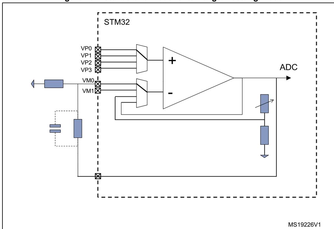
The diagram illustrates an operational amplifier (OPAMP) configured in an inverting mode with external gain setting. The OPAMP is represented by a triangle with '+' and '-' inputs. The non-inverting input (+) is connected to a multiplexer that selects between four reference voltages: VP0, VP1, VP2, and VP3. The inverting input (-) is connected to a summing node. The output of the OPAMP is connected to an ADC and to a feedback network. The feedback network consists of a resistor connected between the output and the summing node, and a capacitor connected between the summing node and ground. An external input signal is applied to the summing node through a resistor and a capacitor. The summing node is also connected to the inverting input (-) of the OPAMP. The entire circuit is enclosed in a dashed box labeled 'STM32'. The diagram is labeled 'MS19226V1' in the bottom right corner.
- 1. This figure gives an example in an inverting configuration. Any other option is possible, including comparator mode.
Follower configuration mode
The amplifier can be configured as a follower, by setting the VM_SEL bits to 11 in the OPAMPx_CR register. This allows you for instance to buffer signals with a relatively high impedance. In this case, the inverting inputs are free and the corresponding ports can be used as regular I/Os.
Figure 132. Follower configuration
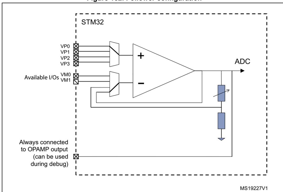
- 1. This figure gives an example in an inverting configuration. Any other option is possible, including comparator mode.
Programmable Gain Amplifier mode
The Programmable Gain Amplifier (PGA) mode is enabled by writing the VM_SEL bits to 10 in the OPAMPx_CR register. The gain is set using the PGA_GAIN bits which must be set to 0x00..0x11 for gains ranging from 2 to 16.
In this case, the inverting inputs are internally connected to the central point of a built-in gain setting resistive network. Figure 133: PGA mode, internal gain setting (x2/x4/x8/x16), inverting input not used shows the internal connection in this mode.
An alternative option in PGA mode allows you to route the central point of the resistive network on one of the I/Os connected to the non-inverting input. This is enabled using the PGA_GAIN bits in OPAMPx_CR register:
- • 10xx values are setting the gain and connect the central point to one of the two available inputs
- • 11xx values are setting the gain and connect the central point to the second available input
This feature can be used for instance to add a low-pass filter to PGA, as shown in Figure 134: PGA mode, internal gain setting (x2/x4/x8/x16), inverting input used for filtering . Please note that the cut-off frequency is changed if the gain is modified (refer to the electrical characteristics section of the datasheet for details on resistive network elements).
Figure 133. PGA mode, internal gain setting (x2/x4/x8/x16), inverting input not used
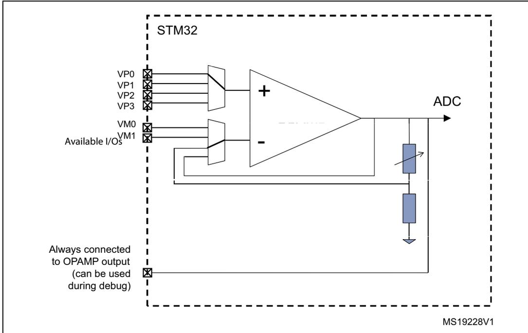
STM32
VP0
VP1
VP2
VP3
Available I/Os
VM0
VM1
ADC
Always connected to OPAMP output (can be used during debug)
MS19228V1
Figure 134. PGA mode, internal gain setting (x2/x4/x8/x16), inverting input used for filtering
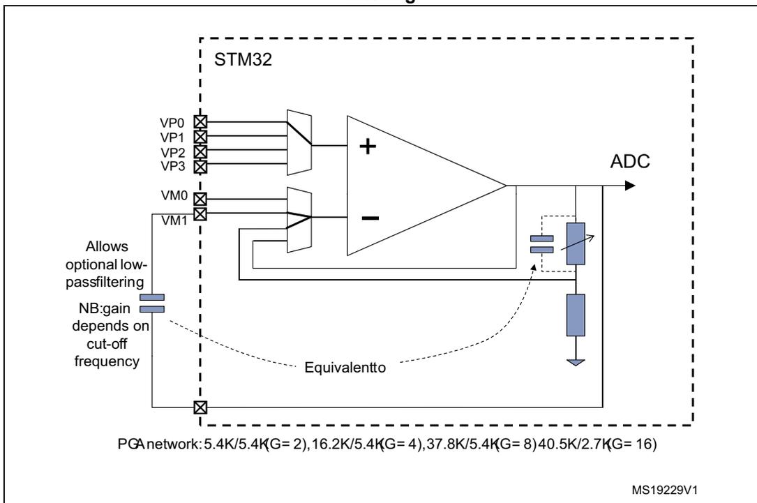
STM32
VP0
VP1
VP2
VP3
VM0
VM1
ADC
Allows optional low-pass filtering
NB: gain depends on cut-off frequency
Equivalent to
PGA network: \( 5.4\text{K}/5.4\text{K} (G=2) \) , \( 16.2\text{K}/5.4\text{K} (G=4) \) , \( 37.8\text{K}/5.4\text{K} (G=8) \) , \( 40.5\text{K}/2.7\text{K} (G=16) \)
MS19229V1
18.4 OPAMP registers
18.4.1 OPAMP1 control register (OPAMP1_CSR)
Note: This register is only available in STM32F303xB/C/D/E, STM32F358xC and STM32F398xE devices.
Address offset : 0x38
Reset value: 0xXXXX 0000
| 31 | 30 | 29 | 28 | 27 | 26 | 25 | 24 | 23 | 22 | 21 | 20 | 19 | 18 | 17 | 16 |
|---|---|---|---|---|---|---|---|---|---|---|---|---|---|---|---|
| LOCK | OUTCAL | TSTR EF | TRIMOFFSETN | TRIMOFFSETP | USER_ TRIM | PGA_GAIN | |||||||||
| rw | r | rw | rw | rw | rw | rw | |||||||||
| 15 | 14 | 13 | 12 | 11 | 10 | 9 | 8 | 7 | 6 | 5 | 4 | 3 | 2 | 1 | 0 |
| PGA_GAIN | CALSEL | CAL ON | VPS_SEL | VMS_SE L | TCM_ EN | VM_SEL | Res. | VP_SEL | FORCE _VP | OPAMP 1EN | |||||
| rw | rw | rw | rw | rw | rw | rw | rw | rw | rw | ||||||
Bit 31 LOCK: OPAMP 1 lock
This bit is write-once. It is set by software. It can only be cleared by a system reset.
This bit is used to configure the OPAMP1_CSR register as read-only.
0: OPAMP1_CSR is read-write.
1: OPAMP1_CSR is read-only.
Bit 30 OUTCAL:
OPAMP output status flag, when the OPAMP is used as comparator during calibration.
0: Non-inverting < inverting
1: Non-inverting > inverting.
Bit 29 TSTREF:
This bit is set and cleared by software. It is used to output the internal reference voltage ( \( V_{REFOPAMP1} \) ).
0: \( V_{REFOPAMP1} \) is output.
1: \( V_{REFOPAMP1} \) is not output.
Bits 28:24 TRIMOFFSETN: Offset trimming value (NMOS)
Bits 23:19 TRIMOFFSETP: Offset trimming value (PMOS)
Bit 18 USER_TRIM: User trimming enable.
This bit is used to configure the OPAMP offset.
0: User trimming disabled.
1: User trimming enabled.
Bits 17:14 PGA_GAIN : Gain in PGA mode
0X00 = Non-inverting gain = 2
0X01 = Non-inverting gain = 4
0X10 = Non-inverting gain = 8
0X11 = Non-inverting gain = 16
1000 = Non-inverting gain = 2 - Internal feedback connected to VM0
1001 = Non-inverting gain = 4 - Internal feedback connected to VM0
1010 = Non-inverting gain = 8 - Internal feedback connected to VM0
1011 = Non-inverting gain = 16 - Internal feedback connected to VM0
1100 = Non-inverting gain = 2 - Internal feedback connected to VM1
1101 = Non-inverting gain = 4 - Internal feedback connected to VM1
1110 = Non-inverting gain = 8 - Internal feedback connected to VM1
1111 = Non-inverting gain = 16 - Internal feedback connected to VM1
Bits 13:12 CALSEL : Calibration selection
This bit is set and cleared by software. It is used to select the offset calibration bus used to generate the internal reference voltage when CALON = 1 or FORCE_VP= 1.
00 = \( V_{REFOPAMP} = 3.3\% V_{DDA} \)
01 = \( V_{REFOPAMP} = 10\% V_{DDA} \)
10 = \( V_{REFOPAMP} = 50\% V_{DDA} \)
11 = \( V_{REFOPAMP} = 90\% V_{DDA} \)
Bit 11 CALON : Calibration mode enable
This bit is set and cleared by software. It is used to enable the calibration mode connecting VM and VP to the OPAMP internal reference voltage.
0: Calibration mode disabled.
1: Calibration mode enabled.
Bits 10:9 VPS_SEL : OPAMP1 Non inverting input secondary selection.
These bits are set and cleared by software. They are used to select the OPAMP1 non inverting input when TCM_EN = 1.
00: PA7 used as OPAMP1 non inverting input
01: PA5 used as OPAMP1 non inverting input
10: PA3 used as OPAMP1 non inverting input
11: PA1 used as OPAMP1 non inverting input
Bit 8 VMS_SEL : OPAMP1 inverting input secondary selection
This bit is set and cleared by software. It is used to select the OPAMP1 inverting input when TCM_EN = 1.
0: PC5 (VM0) used as OPAMP1 inverting input
1: PA3 (VM1) used as OPAMP1 inverting input
Bit 7 TCM_EN : Timer controlled Mux mode enable
This bit is set and cleared by software. It is used to control automatically the switch between the default selection (VP_SEL and VM_SEL) and the secondary selection (VPS_SEL and VMS_SEL) of the inverting and non inverting inputs.
Bits 6:5 VM_SEL : OPAMP1 inverting input selection.
These bits are set and cleared by software. They are used to select the OPAMP1 inverting input.
00: PC5 (VM0) used as OPAMP1 inverting input
01: PA3 (VM1) used as OPAMP1 inverting input
10: Resistor feedback output (PGA mode)
11: follower mode
Bit 4 Reserved, must be kept at reset value.
Bits 3:2 VP_SEL : OPAMP1 Non inverting input selection.
These bits are set and cleared by software. They are used to select the OPAMP1 non inverting input.
- 00: PA7 used as OPAMP1 non inverting input
- 01: PA5 used as OPAMP1 non inverting input
- 10: PA3 used as OPAMP1 non inverting input
- 11: PA1 used as OPAMP1 non inverting input
Bit 1 FORCE_VP :
This bit forces a calibration reference voltage on non-inverting input and disables external connections.
- 0: Normal operating mode. Non-inverting input connected to inputs.
- 1: Calibration mode. Non-inverting input connected to calibration reference voltage.
Bit 0 OPAMP1EN : OPAMP1 enable.
This bit is set and cleared by software. It is used to enable the OPAMP1.
- 0: OPAMP1 is disabled.
- 1: OPAMP1 is enabled.
18.4.2 OPAMP2 control register (OPAMP2_CSR)
Address offset: 0x3C
Reset value: 0xXXXX 0000
| 31 | 30 | 29 | 28 | 27 | 26 | 25 | 24 | 23 | 22 | 21 | 20 | 19 | 18 | 17 | 16 |
|---|---|---|---|---|---|---|---|---|---|---|---|---|---|---|---|
| LOCK | OUT CAL | TSTREF | TRIMOFFSETN | TRIMOFFSETP | USER_TRIM | PGA_GAIN | |||||||||
| rw | r | rw | rw | rw | rw | rw | |||||||||
| 15 | 14 | 13 | 12 | 11 | 10 | 9 | 8 | 7 | 6 | 5 | 4 | 3 | 2 | 1 | 0 |
|---|---|---|---|---|---|---|---|---|---|---|---|---|---|---|---|
| PGA_GAIN | CALSEL | CAL ON | VPS_SEL | VMS_SEL | TCM_EN | VM_SEL | Res. | VP_SEL | FORCE_VP | OPAMP2EN | |||||
| rw | rw | rw | rw | rw | rw | rw | rw | rw | rw | ||||||
Bit 31 LOCK : OPAMP 2 lock
This bit is write-once. It is set by software. It can only be cleared by a system reset.
This bit is used to configure the OPAMP2_CSR register as read-only.
- 0: OPAMP2_CSR is read-write.
- 1: OPAMP2_CSR is read-only.
Bit 30 OUTCAL :
OPAMP output status flag, when the OPAMP is used as comparator during calibration.
- 0: Non-inverting < inverting
- 1: Non-inverting > inverting.
Bit 29 TSTREF :
This bit is set and cleared by software. It is used to output the internal reference voltage ( \( V_{REFOPAMP2} \) ).
- 0: \( V_{REFOPAMP2} \) is output.
- 1: \( V_{REFOPAMP2} \) is not output.
Bits 28:24 TRIMOFFSETN : Offset trimming value (NMOS)
Bits 23:19 TRIMOFFSETP : Offset trimming value (PMOS)
Bit 18 USER_TRIM : User trimming enable.
This bit is used to configure the OPAMP offset.
0: User trimming disabled.
1: User trimming enabled.
Bits 17:14 PGA_GAIN : gain in PGA mode
0X00 = Non-inverting gain = 2
0X01 = Non-inverting gain = 4
0X10 = Non-inverting gain = 8
0X11 = Non-inverting gain = 16
1000 = Non-inverting gain = 2 - Internal feedback connected to VM0
1001 = Non-inverting gain = 4 - Internal feedback connected to VM0
1010 = Non-inverting gain = 8 - Internal feedback connected to VM0
1011 = Non-inverting gain = 16 - Internal feedback connected to VM0
1100 = Non-inverting gain = 2 - Internal feedback connected to VM1
1101 = Non-inverting gain = 4 - Internal feedback connected to VM1
1110 = Non-inverting gain = 8 - Internal feedback connected to VM1
1111 = Non-inverting gain = 16 - Internal feedback connected to VM1
Bits 13:12 CALSEL : Calibration selection
This bit is set and cleared by software. It is used to select the offset calibration bus used to generate the internal reference voltage when CALON = 1 or FORCE_VP= 1.
00 = \( V_{REFOPAMP} = 3.3\% V_{DDA} \)
01 = \( V_{REFOPAMP} = 10\% V_{DDA} \)
10 = \( V_{REFOPAMP} = 50\% V_{DDA} \)
11 = \( V_{REFOPAMP} = 90\% V_{DDA} \)
Bit 11 CALON : Calibration mode enable
This bit is set and cleared by software. It is used to enable the calibration mode connecting VM and VP to the OPAMP internal reference voltage.
0: calibration mode disabled.
1: calibration mode enabled.
Bits 10:9 VPS_SEL : OPAMP2 Non inverting input secondary selection.
These bits are set and cleared by software. They are used to select the OPAMP2 non inverting input when TCM_EN = 1.
00: PD14 used as OPAMP2 non inverting input (STM32F303xB/C and STM32F358C devices only)
01: PB14 used as OPAMP2 non inverting input
10: PB0 used as OPAMP2 non inverting input
11: PA7 used as OPAMP2 non inverting input
Bit 8 VMS_SEL : OPAMP2 inverting input secondary selection
This bit is set and cleared by software. It is used to select the OPAMP2 inverting input when TCM_EN = 1.
0: PC5 (VM0) used as OPAMP2 inverting input
1: PA5 (VM1) used as OPAMP2 inverting input
Bit 7 TCM_EN : Timer controlled Mux mode enable.
This bit is set and cleared by software. It is used to control automatically the switch between the default selection (VP_SEL and VM_SEL) and the secondary selection (VPS_SEL and VMS_SEL) of the inverting and non inverting inputs.
Bits 6:5 VM_SEL : OPAMP2 inverting input selection.
Theses bits are set and cleared by software. They are used to select the OPAMP2 inverting input.
00: PC5 (VM0) used as OPAMP2 inverting input
01: PA5 (VM1) used as OPAMP2 inverting input
10: Resistor feedback output (PGA mode)
11: follower mode
Bit 4 Reserved, must be kept at reset value.
Bits 3:2 VP_SEL : OPAMP2 non inverting input selection.
Theses bits are set/reset by software. They are used to select the OPAMP2 non inverting input.
00: PD14 used as OPAMP2 non inverting input (STM32F303xB/C/D/E, STM32F358xC and STM32F398xE devices only)
01: PB14 used as OPAMP2 non inverting input
10: PB0 used as OPAMP2 non inverting input
11: PA7 used as OPAMP2 non inverting input
Bit 1 FORCE_VP :
This bit forces a calibration reference voltage on non-inverting input and disables external connections.
0: Normal operating mode. Non-inverting input connected to inputs.
1: Calibration mode. Non-inverting input connected to calibration reference voltage.
Bit 0 OPAMP2EN : OPAMP2 enable.
This bit is set and cleared by software. It is used to select the OPAMP2.
0: OPAMP2 is disabled.
1: OPAMP2 is enabled.
18.4.3 OPAMP3 control register (OPAMP3_CSR)
Note: This register is only available in STM32F303xB/C/D/E, STM32F358xC and STM32F398xE devices.
Address offset: 0x40
Reset value: 0xXXXX 0000
| 31 | 30 | 29 | 28 | 27 | 26 | 25 | 24 | 23 | 22 | 21 | 20 | 19 | 18 | 17 | 16 |
|---|---|---|---|---|---|---|---|---|---|---|---|---|---|---|---|
| LOCK | OUT_CAL | TSTR_EF | TRIMOFFSETN | TRIMOFFSETP | USER_TRIM | PGA_GAIN | |||||||||
| rw | r | rw | rw | rw | rw | rw | |||||||||
| 15 | 14 | 13 | 12 | 11 | 10 | 9 | 8 | 7 | 6 | 5 | 4 | 3 | 2 | 1 | 0 |
|---|---|---|---|---|---|---|---|---|---|---|---|---|---|---|---|
| PGA_GAIN | CALSEL | CAL_ON | VPS_SEL | VMS_SEL | TCM_EN | VM_SEL | Res. | VP_SEL | FORCE_VP | OPAMP3EN | |||||
| rw | rw | rw | rw | rw | rw | rw | rw | rw | rw | ||||||
This bit is write-once. It is set by software. It can only be cleared by a system reset.
This bit is used to configure the OPAMP3_CSR register as read-only.
0: OPAMP3_CSR is read-write.
1: OPAMP3_CSR is read-only.
Bit 30 OUTCAL:OPAMP output status flag, when the OPAMP is used as comparator during calibration.
0: Non-inverting < inverting
1: Non-inverting > inverting.
Bit 29 TSTREF:This bit is set and cleared by software. It is used to output the internal reference voltage ( \( V_{REFOPAMP3} \) ).
0: \( V_{REFOPAMP3} \) is output.
1: \( V_{REFOPAMP3} \) is not output.
Bits 28:24 TRIMOFFSETN: Offset trimming value (NMOS) Bits 23:19 TRIMOFFSETP: Offset trimming value (PMOS) Bit 18 USER_TRIM: User trimming enable.This bit is used to configure the OPAMP offset.
0: User trimming disabled.
1: User trimming enabled.
Bits 17:14 PGA_GAIN: gain in PGA mode0X00 = Non-inverting gain = 2
0X01 = Non-inverting gain = 4
0X10 = Non-inverting gain = 8
0X11 = Non-inverting gain = 16
1000 = Non-inverting gain = 2 - Internal feedback connected to VM0
1001 = Non-inverting gain = 4 - Internal feedback connected to VM0
1010 = Non-inverting gain = 8 - Internal feedback connected to VM0
1011 = Non-inverting gain = 16 - Internal feedback connected to VM0
1100 = Non-inverting gain = 2 - Internal feedback connected to VM1
1101 = Non-inverting gain = 4 - Internal feedback connected to VM1
1110 = Non-inverting gain = 8 - Internal feedback connected to VM1
1111 = Non-inverting gain = 16 - Internal feedback connected to VM1
Bits 13:12 CALSEL: Calibration selectionThis bit is set and cleared by software. It is used to select the offset calibration bus used to generate the internal reference voltage when CALON = 1 or FORCE_VP= 1.
00 = \( V_{REFOPAMP} = 3.3\% V_{DDA} \)
01 = \( V_{REFOPAMP} = 10\% V_{DDA} \)
10 = \( V_{REFOPAMP} = 50\% V_{DDA} \)
11 = \( V_{REFOPAMP} = 90\% V_{DDA} \)
Bit 11 CALON: Calibration mode enableThis bit is set/cleared by software. It allows enabling the calibration mode connecting VM and VP to internal reference voltage.
0: calibration mode disabled.
1: calibration mode enabled.
Bits 10:9 VPS_SEL : OPAMP3 non inverting input secondary selection.
These bits are set/reset by software. They allow selecting the OPAMP3 non inverting input when \( TCM\_EN = 1 \) .
00: PB13 used as OPAMP3 non inverting input
01: PA5 used as OPAMP3 non inverting input
10: PA1 used as OPAMP3 non inverting input
11: PB0 used as OPAMP3 non inverting input
Bit 8 VMS_SEL : OPAMP3 inverting input secondary selection
This bit is set and cleared by software. It is used to select the OPAMP3 inverting input when \( TCM\_EN = 1 \) .
0: PB10 (VM0) used as OPAMP3 inverting input
1: PB2 (VM1) used as OPAMP3 inverting input
Bit 7 TCM_EN : Timer controlled multiplexer mode enable.
This bit is set and cleared by software. It is used to control automatically the switch between the default selection (VP_SEL and VM_SEL) and the secondary selection (VPS_SEL and VMS_SEL) of the inverting and non inverting inputs.
Bits 6:5 VM_SEL : OPAMP3 inverting input selection.
These bits are set/reset by software. They allow selecting the OPAMP3 inverting input.
00: PB10 (VM0) used as OPAMP3 inverting input
01: PB2 (VM1) used as OPAMP3 inverting input
10: Resistor feedback output (PGA mode)
11: follower mode
Bit 4 Reserved, must be kept at reset value.
Bits 3:2 VP_SEL : OPAMP3 Non inverting input selection.
These bits are set and cleared by software. They are used to select the OPAMP3 non inverting input.
00: PB13 used as OPAMP3 non inverting input
01: PA5 used as OPAMP3 non inverting input
10: PA1 used as OPAMP3 non inverting input
11: PB0 used as OPAMP3 non inverting input
Bit 1 FORCE_VP :
This bit forces a calibration reference voltage on non-inverting input and disables external connections.
0: Normal operating mode. Non-inverting input connected to inputs.
1: Calibration mode. Non-inverting input connected to calibration reference voltage.
Bit 0 OPAMP3EN : OPAMP3 enable.
This bit is set and cleared by software. It is used to enable the OPAMP3.
0: OPAMP3 is disabled.
1: OPAMP3 is enabled.
18.4.4 OPAMP4 control register (OPAMP4_CSR)
Note: This register is only available in STM32F303xB/C/D/E, STM32F358xC and STM32F398xE devices.
Address offset: 0x44
Reset value: 0xXXXX 0000
| 31 | 30 | 29 | 28 | 27 | 26 | 25 | 24 | 23 | 22 | 21 | 20 | 19 | 18 | 17 | 16 |
|---|---|---|---|---|---|---|---|---|---|---|---|---|---|---|---|
| LOCK | OUT CAL | TSTR EF | TRIMOFFSETN | TRIMOFFSETP | USER_ TRIM | PGA_GAIN | |||||||||
| rw | r | rw | rw | rw | rw | rw | |||||||||
| 15 | 14 | 13 | 12 | 11 | 10 | 9 | 8 | 7 | 6 | 5 | 4 | 3 | 2 | 1 | 0 |
| PGA_GAIN | CALSEL | CAL ON | VPS_SEL | VMS_ SEL | TCM_ EN | VM_SEL | Res. | VP_SEL | FORCE _VP | OPAMP 4EN | |||||
| rw | rw | rw | rw | rw | rw | rw | rw | rw | rw | ||||||
Bit 31 LOCK: OPAMP 4 lock
This bit is write-once. It is set by software. It can only be cleared by a system reset.
This bit is used to configure the OPAMP4_CSR register as read-only.
0: OPAMP4_CSR is read-write.
1: OPAMP4_CSR is read-only.
Bit 30 OUTCAL:
OPAMP output status flag, when the OPAMP is used as comparator during calibration.
0: Non-inverting < inverting
1: Non-inverting > inverting.
Bit 29 TSTREF:
This bit is set and cleared by software. It is used to output the internal reference voltage ( \( V_{REFOPAMP4} \) ).
0: \( V_{REFOPAMP4} \) is output.
1: \( V_{REFOPAMP4} \) is not output.
Bits 28:24 TRIMOFFSETN: Offset trimming value (NMOS)
Bits 23:19 TRIMOFFSETP: Offset trimming value (PMOS)
Bit 18 USER_TRIM: User trimming enable.
This bit is used to configure the OPAMP offset.
0: User trimming disabled.
1: User trimming enabled.
Bits 17:14 PGA_GAIN : Gain in PGA mode
0X00 = Non-inverting gain = 2
0X01 = Non-inverting gain = 4
0X10 = Non-inverting gain = 8
0X11 = Non-inverting gain = 16
1000 = Non-inverting gain = 2 - Internal feedback connected to VM0
1001 = Non-inverting gain = 4 - Internal feedback connected to VM0
1010 = Non-inverting gain = 8 - Internal feedback connected to VM0
1011 = Non-inverting gain = 16 - Internal feedback connected to VM0
1100 = Non-inverting gain = 2 - Internal feedback connected to VM1
1101 = Non-inverting gain = 4 - Internal feedback connected to VM1
1110 = Non-inverting gain = 8 - Internal feedback connected to VM1
1111 = Non-inverting gain = 16 - Internal feedback connected to VM1
Bits 13:12 CALSEL : Calibration selection
This bit is set and cleared by software. It is used to select the offset calibration bus used to generate the internal reference voltage when CALON = 1 or FORCE_VP= 1.
00 =
\(
V_{REFOPAMP} = 3.3\% V_{DDA}
\)
01 =
\(
V_{REFOPAMP} = 10\% V_{DDA}
\)
10 =
\(
V_{REFOPAMP} = 50\% V_{DDA}
\)
11 =
\(
V_{REFOPAMP} = 90\% V_{DDA}
\)
Bit 11 CALON : Calibration mode enable
This bit is set and cleared by software. It is used to enable the calibration mode connecting VM and VP to the OPAMP internal reference voltage.
0: Calibration mode disabled.
1: Calibration mode enabled.
Bits 10:9 VPS_SEL : OPAMP4 Non inverting input secondary selection.
These bits are se and cleared by software. They allow selecting the OPAMP4 non inverting input, when TCM_EN = 1.
00: PD11 used as OPAMP4 non inverting input
01: PB11 used as OPAMP4 non inverting input
10: PA4 used as OPAMP4 non inverting input
11: PB13 used as OPAMP4 non inverting input
Bit 8 VMS_SEL : OPAMP4 inverting input secondary selection
This bit is set and cleared by software. It allows selecting the OPAMP4 inverting input, when TCM_EN = 1.
0: PB10 (VM0) used as OPAMP4 inverting input
1: PD8 (VM1) used as OPAMP4 inverting input
Bit 7 TCM_EN : Timer controlled Mux mode enable
This bit is set and cleared by software. It is used to control automatically the switch between the default selection (VP_SEL and VM_SEL) and the secondary selection (VPS_SEL and VMS_SEL) of the inverting and non inverting inputs.
Bits 6:5 VM_SEL : OPAMP4 inverting input selection.
Theses bits are set/reset by software. They allow selecting the OPAMP4 inverting input.
00: PB10 (VM0) used as OPAMP4 inverting input
01: PD8 (VM1) used as OPAMP4 inverting input
10: Resistor feedback output (PGA mode)
11: follower mode
Bit 4 Reserved, must be kept at reset value.
Bits 3:2 VP_SEL : OPAMP4 Non inverting input selection.
These bits are set and cleared by software. They allow selecting the OPAMP4 non inverting input.
00: PD11 used as OPAMP4 non inverting input
01: PB11 used as OPAMP4 non inverting input
10: PA4 used as OPAMP4 non inverting input
11: PB13 used as OPAMP4 non inverting input
Bit 1 FORCE_VP :
This description will be given in a future version of this document.
Bit 0 OPAMP4EN : OPAMP4 enable.
This bit is set and cleared by software. It allows enabling the OPAMP4.
0: OPAMP4 is disabled.
1: OPAMP4 is enabled.
18.4.5 OPAMP register map
The following table summarizes the OPAMP registers.
Table 112. OPAMP register map and reset values
| Offset | Register | 31 | 30 | 29 | 28 | 27 | 26 | 25 | 24 | 23 | 22 | 21 | 20 | 19 | 18 | 17 | 16 | 15 | 14 | 13 | 12 | 11 | 10 | 9 | 8 | 7 | 6 | 5 | 4 | 3 | 2 | 1 | 0 |
|---|---|---|---|---|---|---|---|---|---|---|---|---|---|---|---|---|---|---|---|---|---|---|---|---|---|---|---|---|---|---|---|---|---|
| 0x38 | OPAMP1_CSR | LOCK | OUTCAL | TSTREF | TRIMOFFSETH | TRIMOFFSETL | USER_TRIM | PGA_GAIN | CALSEL | CALON | VPS_SEL | VMS_SEL | TOM_EN | VM_SEL | Res | VP_SEL | FORCE_VP | OPAMP1EN | |||||||||||||||
| Reset value | X | X | X | X | X | X | X | X | X | X | X | X | X | X | X | X | 0 | 0 | 0 | 0 | 0 | 0 | 0 | 0 | 0 | 0 | 0 | 0 | 0 | 0 | 0 | 0 | |
| 0x3C | OPAMP2_CSR | LOCK | OUTCAL | TSTREF | TRIMOFFSETH | TRIMOFFSETL | USER_TRIM | PGA_GAIN | CALSEL | CALON | VPS_SEL | VMS_SEL | TOM_EN | VM_SEL | Res | VP_SEL | FORCE_VP | OPAMP2EN | |||||||||||||||
| Reset value | X | X | X | X | X | X | X | X | X | X | X | X | X | X | X | X | 0 | 0 | 0 | 0 | 0 | 0 | 0 | 0 | 0 | 0 | 0 | 0 | 0 | 0 | 0 | 0 | |
| 0x40 | OPAMP3_CSR | LOCK | OUTCAL | TSTREF | TRIMOFFSETH | TRIMOFFSETL | USER_TRIM | PGA_GAIN | CALSEL | CALON | VPS_SEL | VMS_SEL | TOM_EN | VM_SEL | Res | VP_SEL | FORCE_VP | OPAMP3EN | |||||||||||||||
| Reset value | X | X | X | X | X | X | X | X | X | X | X | X | X | X | X | X | 0 | 0 | 0 | 0 | 0 | 0 | 0 | 0 | 0 | 0 | 0 | 0 | 0 | 0 | 0 | 0 | |
| 0x44 | OPAMP4_CSR | LOCK | OUTCAL | TSTREF | TRIMOFFSETH | TRIMOFFSETL | USER_TRIM | PGA_GAIN | CALSEL | CALON | VPS_SEL | VMS_SEL | TOM_EN | VM_SEL | Res | VP_SEL | FORCE_VP | OPAMP4EN | |||||||||||||||
| Reset value | X | X | X | X | X | X | X | X | X | X | X | X | X | X | X | X | 0 | 0 | 0 | 0 | 0 | 0 | 0 | 0 | 0 | 0 | 0 | 0 | 0 | 0 | 0 | 0 |
Refer to Section 3.2 on page 53 for the register boundary addresses.