17. Comparator (COMP)
17.1 Introduction
STM32F303xB/C/D/E, STM32F358xx and STM32F398xx embed seven general purpose comparators that can be used either as standalone devices (all terminal are available on I/Os) or combined with the timers. STM32F303x6/8 and STM32F328x8 embed three comparators, COMP2, COMP4 and COMP6.
The comparators can be used for a variety of functions including:
- • Wake-up from low-power mode triggered by an analog signal,
- • Analog signal conditioning,
- • Cycle-by-cycle current control loop when combined with the DAC and a PWM output from a timer.
17.2 COMP main features
- • Rail-to-rail comparators
- • Each comparator has positive and configurable negative inputs used for flexible voltage selection:
- – Multiplexed I/O pins
- – DAC1 channel 1, DAC1 channel 2, DAC2 channel1 on STM32F303x6/8 and STM32F328x8 devices and DAC1 channel 1, DAC1 channel 2 on STM32F303xB/C/D/E, STM32F358xx and STM32F398xx devices.
- – Internal reference voltage and three submultiple values (1/4, 1/2, 3/4) provided by scaler (buffered voltage divider)
- • Programmable hysteresis (on STM32F303xB/C and STM32F358xC only)
- • Programmable speed / consumption (on STM32F303xB/C and STM32F358xC only)
- • The outputs can be redirected to an I/O or to timer inputs for triggering:
- – Capture events
- – OCREF_CLR events (for cycle-by-cycle current control)
- – Break events for fast PWM shutdowns
- • COMP1/COMP2, COMP3/COMP4 and COMP5/COMP6 comparators can be combined in a window comparator. This applies to STM32F303xB/C and STM32F358xC devices only. COMP7 does not support the window mode.
- • Comparator outputs with blanking source
- • Each comparator has interrupt generation capability with wake-up from Sleep and Stop modes (through the EXTI controller)
17.3 COMP functional description
17.3.1 COMP block diagram
The block diagram of the comparators is shown in Figure 122: Comparator 1 and 2 block diagrams (STM32F303xB/C/D/E, STM32F358xC and STM32F398xE) and Figure 123: STM32F303xB/C/D/E, STM32F358xC and STM32F398xE comparator 7 block diagram .
Figure 122. Comparator 1 and 2 block diagrams (STM32F303xB/C/D/E, STM32F358xC and STM32F398xE)
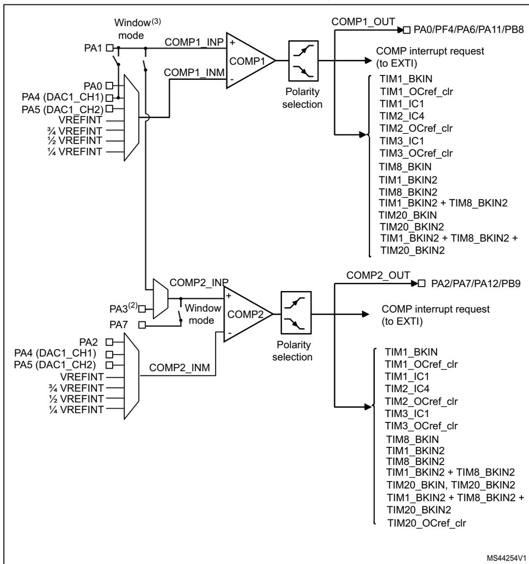
- 1. For a complete block diagram of comparators 1 to 6, refer to Section 18: Operational amplifier (OPAMP) , where all block diagrams and interconnections between comparators 1 to 6 and operational amplifiers are given.
- 2. Only on STM32F303xB/C and STM32F358xC.
- 3. Window mode is not supported in STM32F303xD/E and STM32F398xE.
Figure 123. STM32F303xB/C/D/E, STM32F358xC and STM32F398xE comparator 7 block diagram
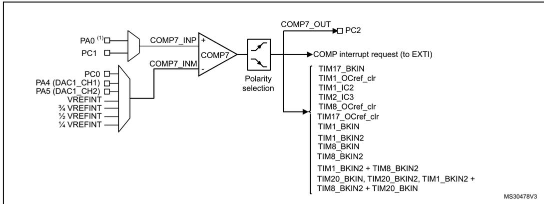
The diagram illustrates the internal structure of comparator 7 (COMP7). The non-inverting input (COMP7_INP) is connected to PA0 (1) or PC1. The inverting input (COMP7_INM) is connected to a multiplexer that selects between PC0, PA4 (DAC1_CH1), PA5 (DAC1_CH2), VREFINT, 3/4 VREFINT, 1/2 VREFINT, and 1/4 VREFINT. The output (COMP7_OUT) is connected to PC2 and provides a COMP interrupt request (to EXTI). The output is also connected to a list of timer and interrupt signals: TIM17_BKIN, TIM1_OCref_clr, TIM1_IC2, TIM2_IC3, TIM8_OCref_clr, TIM17_OCref_clr, TIM1_BKIN, TIM1_BKIN2, TIM8_BKIN, TIM8_BKIN2, TIM1_BKIN2 + TIM8_BKIN2, TIM20_BKIN, TIM20_BKIN2, TIM1_BKIN2 + TIM8_BKIN2 + TIM20_BKIN. The identifier MS30478V3 is shown in the bottom right corner.
1. Only for STM32F303xB/C and STM32F358xC
Figure 124. STM32F303x6/8 and STM32F328x8 comparators 2/4/6 block diagrams
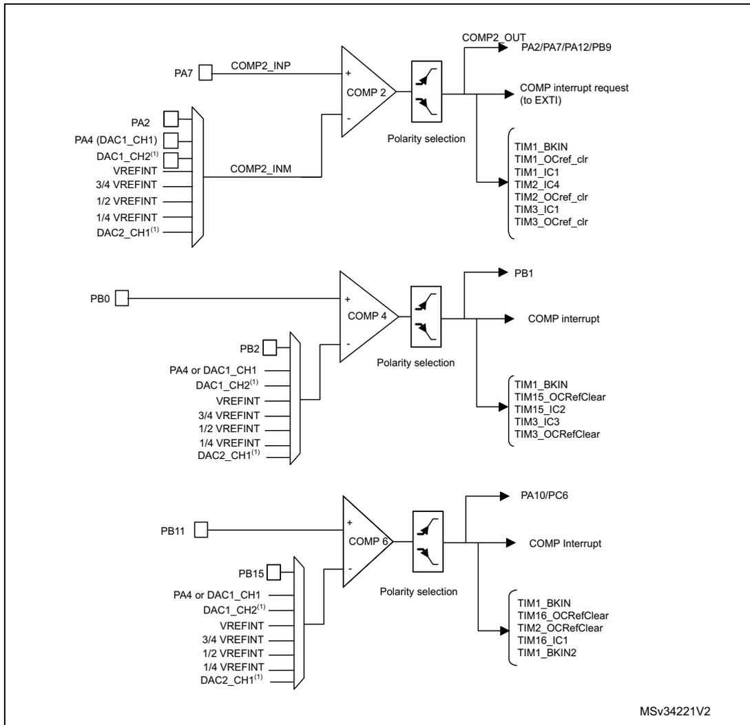
The diagram shows three comparator blocks: COMP2, COMP4, and COMP6.
- COMP2: INP is PA7, INM is a multiplexer (PA2, PA4 (DAC1_CH1), DAC1_CH2
(1)
, VREFINT, 3/4 VREFINT, 1/2 VREFINT, 1/4 VREFINT, DAC2_CH1
(1)
). Output (COMP2_OUT) is PA2/PA7/PA12/PB9. Signals include TIM1_BKIN, TIM1_OCref_clr, TIM1_IC1, TIM2_IC4, TIM2_OCref_clr, TIM3_IC1, TIM3_OCref_clr.
- COMP4: INP is PB0, INM is a multiplexer (PB2, PA4 or DAC1_CH1, DAC1_CH2
(1)
, VREFINT, 3/4 VREFINT, 1/2 VREFINT, 1/4 VREFINT, DAC2_CH1
(1)
). Output (COMP4_OUT) is PB1. Signals include TIM1_BKIN, TIM15_OCRefClear, TIM15_IC2, TIM3_IC3, TIM3_OCRefClear.
- COMP6: INP is PB11, INM is a multiplexer (PB15, PA4 or DAC1_CH1, DAC1_CH2
(1)
, VREFINT, 3/4 VREFINT, 1/2 VREFINT, 1/4 VREFINT, DAC2_CH1
(1)
). Output (COMP6_OUT) is PA10/PC6. Signals include TIM1_BKIN, TIM16_OCRefClear, TIM2_OCRefClear, TIM16_IC1, TIM1_BKIN2.
The identifier MSv34221V2 is shown in the bottom right corner.
1. In STM32F303x6/8 and STM32F328x8 devices, DAC1_CH2 and DAC2_CH1 outputs are connected
directly, thus PA5 and PA6 are not available as COMP x _INM (x = 2,4,6) inputs. When DAC1_OUT2 and DAC2_OUT1 are connected internally to comparator non inverting input, the I/Os on which the DAC1_OUT and DAC2_OUT1 are mapped (PA5 and PA6) can be used as GPIOs.
17.3.2 COMP pins and internal signals
The I/Os used as comparators inputs must be configured in analog mode in the GPIOs registers.
The comparator output can be connected to the I/Os using the alternate function channel given in “Alternate function mapping” table in the datasheet.
The table below summarizes the I/Os that can be used as comparators inputs and outputs.
The output can also be internally redirected to a variety of timer input for the following purposes:
- • Emergency shut-down of PWM signals, using BKIN and BKIN2 inputs
- • Cycle-by-cycle current control, using OCREF_CLR inputs
- • Input capture for timing measures
It is possible to have the comparator output simultaneously redirected internally and externally.
Table 108. Comparator input/output summary
| Comparator inputs/outputs | |||||||
|---|---|---|---|---|---|---|---|
| COMP1 | COMP2 | COMP3 | COMP4 | COMP5 | COMP6 | COMP7 (3) | |
| Comparator inverting input: connection to internal signals | DAC1_CH1 DAC1_CH2 DAC2_CH1 (1) Vrefint \( \frac{3}{4} \) Vrefint \( \frac{1}{2} \) Vrefint \( \frac{1}{4} \) Vrefint | ||||||
| Comparator inputs connected to I/Os (+: non inverting input; -: inverting input) | +: PA1 -: PA0 | +: PA3
(2) +: PA7 -: PA2 | -: PB12 -: PD15 (3) +: PB14 +: PD14 (2) | +: PB0 +: PE7 (2) -: PB2 -: PE8 (3) | -: PB10 -: PD13 (3) +: PB13 +: PD12 (2) | +: PB11 +: PD11 -: PB15 -: PD10 (3) | +: PC1 +: PA0 (2) -: PC0 |
| Comparator outputs (motor control protection) | T1BKIN T1BKIN2 T8BKIN T8BKIN2 T1BKIN2+ T8BKIN2 TIM20BKIN TIM20BKIN2 TIM1BKIN2 + TIM8BKIN2 + TIM20BKIN2 | ||||||
Table 108. Comparator input/output summary (continued)
| Comparator inputs/outputs | |||||||
|---|---|---|---|---|---|---|---|
| COMP1 | COMP2 | COMP3 | COMP4 | COMP5 | COMP6 | COMP7 (3) | |
| Outputs on I/Os | PA0 PF4 PA6 PA11 PB8 | PA2 PA7 (2) PA12 PB9 | PC8 PA8 | PB1 | PC7 PA9 | PA10 PC6 | PC2 |
| Outputs to internal signals | TIM1_OCrefClear TIM1_IC1 TIM2_IC4 TIM2_OCrefClear TIM3_IC1 TIM3_OCrefClear TIM20_OCref_clr (4) | TIM1_OCrefClear TIM2_OCrefClear TIM3_IC2 TIM4_IC1 TIM15_IC1 TIM15_BKIN | TIM8_OCrefClear TIM3_IC3 TIM3_OCrefClear TIM4_IC2 TIM15_OCrefClear TIM15_IC2 | TIM8_OCrefClear TIM2_IC1 TIM3_OCrefClear TIM4_IC3 TIM16_BKIN TIM17_IC1 | TIM8_OCrefClear TIM2_IC2 TIM2_OCrefClear TIM16_OCrefClear TIM16_IC1 TIM4_IC4 | TIM1_OCrefClear TIM8_OCrefClear TIM2_IC3 TIM1_IC2 TIM17_OCrefClear TIM17_BKIN | |
- 1. Only on STM32F303x6/8 and STM32F328x8 devices
- 2. Only on STM32F303xB/C and STM32F358xC devices.
- 3. Only on STM32F303xB/C/D/E, STM32F358xC and STM32F398xE devices.
- 4. Only on COMP2 on STM32F303x/D/E and STM32F398xE devices.
17.3.3 COMP reset and clocks
The COMP clock provided by the clock controller is synchronous with the PCLK2 (APB2 clock).
There is no clock enable control bit provided in the RCC controller. To use a clock source for the comparator, the SYSCFG clock enable control bit must be set in the RCC controller.
Important: The polarity selection logic and the output redirection to the port works independently from the PCLK2 clock. This allows the comparator to work even in Stop mode.
17.3.4 Comparator LOCK mechanism
The comparators can be used for safety purposes, such as over-current or thermal protection. For applications having specific functional safety requirements, it is necessary to insure that the comparator programming cannot be altered in case of spurious register access or program counter corruption.
For this purpose, the comparator control and status registers can be write-protected (read-only).
Once the programming is completed, using bits 30:0 of COMPx_CSR, the COMPx LOCK bit can be set to 1. This causes the whole COMPx_CSR register to become read-only, including the COMPx LOCK bit.
The write protection can only be reset by a MCU reset.
17.3.5 Hysteresis (on STM32F303xB/C and STM32F358xC only)
The comparator includes a programmable hysteresis to avoid spurious output transitions in case of noisy signals. The hysteresis can be disabled if it is not needed (for instance when exiting from low-power mode) to be able to force the hysteresis value using external components.
Figure 125. Comparator hysteresis
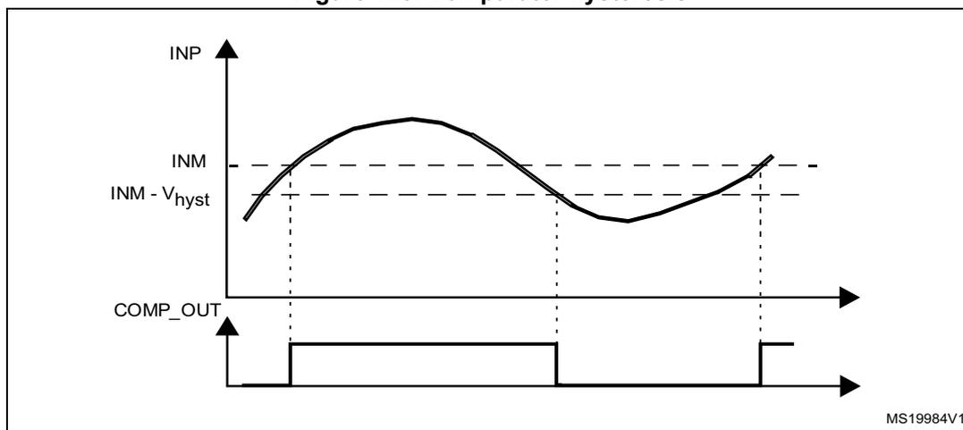
The figure illustrates the hysteresis effect in a comparator. The top graph shows the non-inverting input (INP) as a smooth curve and the inverting input (INM) as a dashed horizontal reference line. A second dashed horizontal line, labeled \( INM - V_{hyst} \) , represents the lower threshold for the hysteresis. The bottom graph shows the COMP_OUT signal as a square wave. The output transitions from low to high when INP rises above INM and from high to low when INP falls below \( INM - V_{hyst} \) . Vertical dashed lines connect the input transitions to the output transitions. The identifier MS19984V1 is in the bottom right corner.
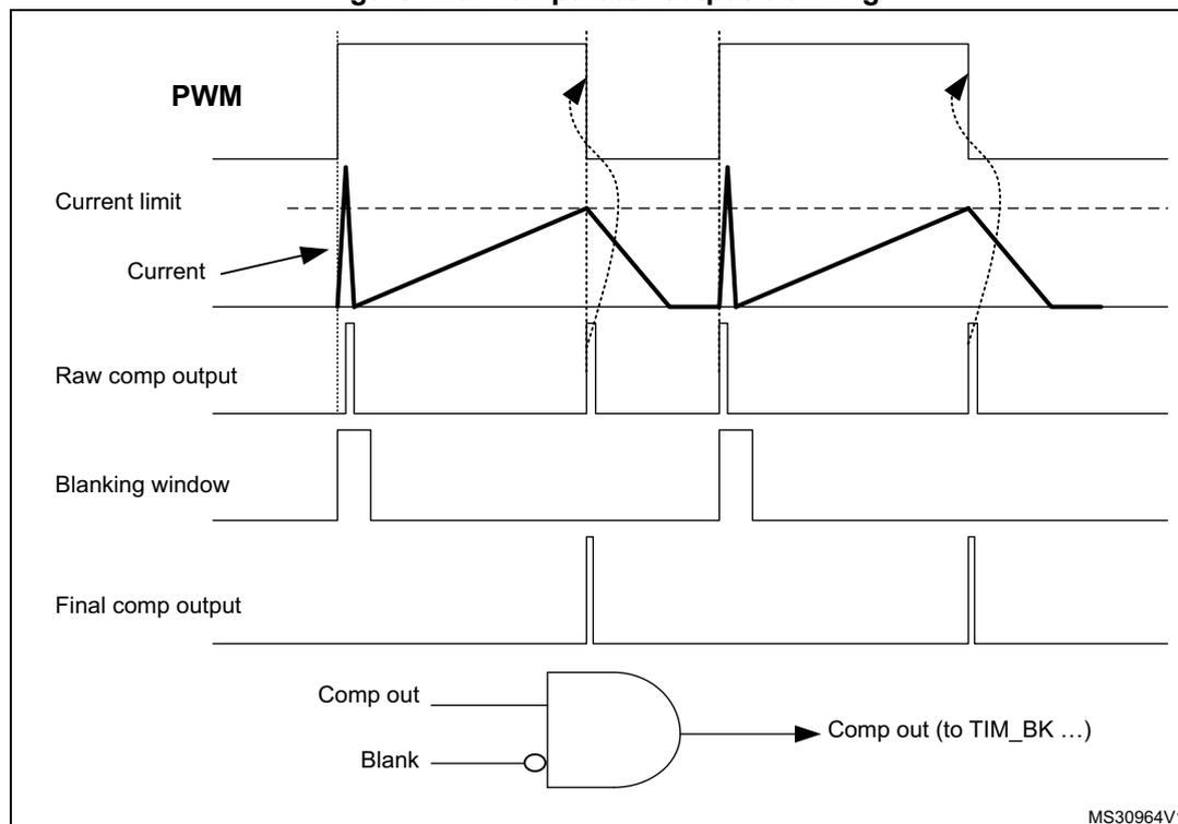
17.3.6 Comparator output blanking function
The purpose of the blanking function is to prevent the current regulation to trip upon short current spikes at the beginning of the PWM period (typically the recovery current in power switches anti parallel diodes). It consists of a selection of a blanking window which is a timer output compare signal. The selection is done by software (refer to the comparator register description for possible blanking signals). Then, the complementary of the blanking signal is ANDed with the comparator output to provide the wanted comparator output. See the example provided in the figure below.
Figure 126. Comparator output blanking
17.3.7 Power mode (STM32F303xB/C and STM32F358xC only)
The comparator power consumption versus propagation delay can be adjusted to have the optimum trade-off for a given application. The bits COMPxMODE[1:0] in COMPx_CSR registers can be programmed as follows:
- • 00: High speed / full power
- • 01: Medium speed / medium power
- • 10: Low speed / low-power
- • 11: Very-low speed / ultra-low-power
17.4 COMP interrupts
The comparator outputs are internally connected to the Extended interrupts and events controller. Each comparator has its own EXTI line and can generate either interrupts or events. The same mechanism is used to exit from low-power modes.
Refer to Interrupt and events section for more details.
17.5 COMP registers
17.5.1 COMP1 control and status register (COMP1_CSR)
Note: This register is available in STM32F303xB/C/D/E, STM32F358xC and STM32F398xE only
Address offset: 0x1C
Reset value: 0x0000 0000
| 31 | 30 | 29 | 28 | 27 | 26 | 25 | 24 | 23 | 22 | 21 | 20 | 19 | 18 | 17 | 16 |
|---|---|---|---|---|---|---|---|---|---|---|---|---|---|---|---|
| COMP1 LOCK | COMP1 OUT | Res. | Res. | Res. | Res. | Res. | Res. | Res. | Res. | Res. | COMP1_ BLANKING | COMP1HYST [1:0] (1) | |||
| rwo | r | rw | rw | rw | rw | rw | |||||||||
| 15 | 14 | 13 | 12 | 11 | 10 | 9 | 8 | 7 | 6 | 5 | 4 | 3 | 2 | 1 | 0 |
|---|---|---|---|---|---|---|---|---|---|---|---|---|---|---|---|
| COMP1 POL | Res. | COMP1OUTSEL | Res. | Res. | Res. | COMP1INMSEL[2:0] | COMP1MODE [1:0] (1) | COMP 1_INP_ DAC | COMP 1EN | ||||||
| rw | rw | rw | rw | rw | rw | rw | rw | rw | rw | rw | rw | ||||
1. Only in STM32F303xB/C and STM32F358xC.
Bit 31 COMP1LOCK : Comparator 1 lock
This bit is write-once. It is set by software. It can only be cleared by a system reset.
It allows to have COMP1_CSR register as read-only.
0: COMP1_CSR is read-write.
1: COMP1_CSR is read-only.
Bit 30 COMP1OUT : Comparator 1 output
This read-only bit is a copy of comparator 1 output state.
0: Output is low (non-inverting input below inverting input).
1: Output is high (non-inverting input above inverting input).
Bits 29:21 Reserved, must be kept at reset value.
Bits 20:18 COMP1_BLANKING : Comparator 1 blanking source
These bits select which Timer output controls the comparator 1 output blanking.
000: No blanking
001: TIM1_OC5 selected as blanking source
010: TIM2_OC3 selected as blanking source
011: TIM3_OC3 selected as blanking source
Other configurations: reserved
Bits 17:16 COMP1HYST[1:0] Comparator 1 hysteresis
On the STM32F303xB/C and STM32F358xC, these bits control the hysteresis level.
00: No hysteresis
01: Low hysteresis
10: Medium hysteresis
11: High hysteresis
Please refer to the electrical characteristics for the hysteresis values.
On the STM32F303xD/E and STM32F398xE, these bits are reserved and must be kept at reset value.
Bit 15 COMP1POL : Comparator 1 output polarity
This bit is used to invert the comparator 1 output.
0: Output is not inverted
1: Output is inverted
Bit 14 Reserved, must be kept at reset value.
Bits 13:10 COMP1OUTSEL[3:0] : Comparator 1 output selectionThese bits select which Timer input must be connected with the comparator1 output.
0000: No selection
0001: (BRK_ACTH) Timer 1 break input
0010: (BRK2) Timer 1 break input 2
0011: Timer 8 break input 1
0100: Timer 8 break input 2
0101: Timer 1 break input 2 + Timer 8 break input 2
0110: Timer 1 OCrefclear input
0111: Timer 1 input capture 1
1000: Timer 2 input capture 4
1001: Timer 2 OCrefclear input
1010: Timer 3 input capture 1
1011: Timer 3 OCrefclear input
1100: Timer 20 break input 1
1101: Timer 20 break input 2
1110: Timer 1 break input 2 + Timer 8 break input 2 + Timer 20 break input 2
1111: Reserved.
Note: Depending on the product, when a timer is not available, the corresponding combination is reserved.
Bits 9:7 Reserved, must be kept at reset value.
Bits 6:4 COMP1INMSEL[2:0] : Comparator 1 inverting input selectionThese bits allows to select the source connected to the inverting input of the comparator 1.
000: 1/4 of Vrefint
001: 1/2 of Vrefint
010: 3/4 of Vrefint
011: Vrefint
100: PA4 or DAC1 output if enabled
101: PA5 or DAC2 output if enabled
110: PA0
111: Reserved
Bits 3:2 COMP1MODE[1:0] : Comparator 1 mode (only in STM32F303xB/C and STM32F358xC devices)These bits control the operating mode of the comparator1 and allows to adjust the speed/consumption.
00: High speed
01: Medium speed
10: Low-power
11: Ultra-low-power
Bit 1 COMP1_INP_DAC : Comparator 1 non inverting input connection to DAC output.This bit closes a switch between comparator 1 non-inverting input (PA0) and DAC out I/O (PA4).
0: Switch open
1: Switch closed
Note: This switch is solely intended to redirect signals onto high impedance input, such as COMP1 non-inverting input (highly resistive switch).
Bit 0 COMP1EN : Comparator 1 enableThis bit switches COMP1 ON/OFF.
0: Comparator 1 disabled
1: Comparator 1 enabled
17.5.2 COMP2 control and status register (COMP2_CSR)
Address offset: 0x20
Reset value: 0x0000 0000
| 31 | 30 | 29 | 28 | 27 | 26 | 25 | 24 | 23 | 22 | 21 | 20 | 19 | 18 | 17 | 16 |
|---|---|---|---|---|---|---|---|---|---|---|---|---|---|---|---|
| COMP2LOCK | COMP2OUT | Res. | Res. | Res. | Res. | Res. | Res. | Res. | COMP2INMSEL[3] (1) | Res. | COMP2_BLANKING[2:0] | COMP2HYST[1:0] (2) | |||
| rwo | r | rw | rw | rw | rw | rw | rw | ||||||||
| 15 | 14 | 13 | 12 | 11 | 10 | 9 | 8 | 7 | 6 | 5 | 4 | 3 | 2 | 1 | 0 |
|---|---|---|---|---|---|---|---|---|---|---|---|---|---|---|---|
| COMP2POL | Res. | COMP2OUTSEL[3:0] | COMP2WINMODE (2) | Res. | COMP2INPSEL (2) | COMP2INMSEL[2:0] | COMP2MODE[1:0] (2) | Res. | COMP2EN | ||||||
| rw | rw | rw | rw | rw | rw | rw | rw | rw | rw | rw | rw | rw | |||
- 1. Only in STM32F303x6/8 and STM32F328x8.
- 2. Only in STM32F303xB/C and STM32F358xC devices.
Bit 31 COMP2LOCK : Comparator 2 lock
This bit is write-once. It is set by software. It can only be cleared by a system reset.
It allows to have COMP2_CSR register as read-only.
0: COMP2_CSR is read-write.
1: COMP2_CSR is read-only.
Bit 30 COMP2OUT : Comparator 2 output
This read-only bit is a copy of comparator 1 output state.
0: Output is low (non-inverting input below inverting input).
1: Output is high (non-inverting input above inverting input).
Bits 29:23 Reserved, must be kept at reset value.
Bit 22 COMP2INMSEL[3] : Comparator 2 inverting input selection. This bit is available only on F303x6/x8 and F328xx. It is used with Bits [6..4] to configure the Comp inverting input.
Bit 21 Reserved, must be kept at reset value.
Bits 20:18 COMP2_BLANKING[2:0] : Comparator 2 output blanking source
These bits select which Timer output controls the comparator 1 output blanking.
000: No blanking
001: TIM1 OC5 selected as blanking source
010: TIM2 OC3 selected as blanking source
011: TIM3 OC3 selected as blanking source
Other configurations: reserved
Bits 17:16 COMP2HYST[1:0] : Comparator 2 Hysteresis
On the STM32F303xB/C and STM32F358xC, these bits control the hysteresis level.
00: No hysteresis
01: Low hysteresis
10: Medium hysteresis
11: High hysteresis
Please refer to the electrical characteristics for the hysteresis values.
On the STM32F303xD/E, STM32F303x6/8, STM32F328x8 and STM32F398xx, these bits are reserved and must be kept at reset value.
Bit 15 COMP2POL : Comparator 2 output polarity
This bit is used to invert the comparator 2 output.
0: Output is not inverted
1: Output is inverted
Bit 14 Reserved, must be kept at reset value.
Bits 13:10 COMP2OUTSEL[3:0] : Comparator 2 output selection
These bits select which Timer input must be connected with the comparator2 output.
0000: No selection
0001: (BRK_ACTH) Timer 1 break input
0010: (BRK2) Timer 1 break input 2
0011: (BRK_ACTH) Timer 8 break input
0100: (BRK2) Timer 8 break input 2
0101: Timer 1 break input2 + Timer 8 break input 2
0110: Timer 1 OCrefclear input
0111: Timer 1 input capture 1
1000: Timer 2 input capture 4
1001: Timer 2 OCrefclear input
1010: Timer 3 input capture 1
1011: Timer 3 OCrefclear input
1100: Timer 20 Break Input selected
1101: Timer 20 Break2 Input selected
1110: Timer 1 Break2 or Timer 8 Break2 or Timer 20 Break2
1111: Timer 20 OCrefClear Input selected
Note: Depending on the product, when a timer is not available, the corresponding combination is reserved.
Bit 9 COMP2WINMODE : Comparator 2 window mode (only in STM32F303xB/C and STM32F358xC devices)
This bit selects the window mode: Both non inverting inputs of comparators share the non inverting input of Comparator 1 (PA1).
0: Comparators 1 and 2 can not be used in window mode.
1: Comparators 1 and 2 can be used in window mode.
Bit 8 Reserved, must be kept at reset value.
Bit 7 COMP2INPSEL : Comparator 2 non inverting input selection (Only in STM32F303xB/C and STM32F358xC devices)
0: PA7 is selected.
1: PA3 is selected.
Note: On STM32F303x6/8, STM32F303xDxE, STM32F398xE and STM32F328, this bit is reserved. COMP2_VINP is available on PA7 whatever value is written in bit 7.
Bits 6:4 COMP2INMSEL[2:0] : Comparator 2 inverting input selection
These bits, together with bit 22, allows to select the source connected to the inverting input of the comparator 2.
0000: 1/4 of Vrefint
0001: 1/2 of Vrefint
0010: 3/4 of Vrefint
0011: Vrefint
0100: PA4 or DAC1_CH1 output if enabled
STM32F303xB/C/D/E, STM32F358xC and STM32F398xC:
0101: PA5 or DAC1_CH2 output if enabled
STM32F303x6/8 and STM32F328x8:
0101: DAC1_CH2 output
0110: PA2
1000: DAC2_CH1 output
Remaining combinations: reserved.
Bits 3:2 COMP2MODE[1:0] : Comparator 2 mode (only in STM32F303xB/C and STM32F358xC devices)
These bits control the operating mode of the comparator2 and allows to adjust the speed/consumption.
00: High speed
01: Medium speed
10: Low-power
11: Ultra-low-power
Bit 1 Reserved, must be kept at reset value.
Bit 0 COMP2EN : Comparator 2 enable
This bit switches COMP2 ON/OFF.
0: Comparator 2 disabled
1: Comparator 2 enabled
17.5.3 COMP3 control and status register (COMP3_CSR)
Note: This register is available in STM32F303xB/C/D/E, STM32F358xx and STM32F398xx only.
Address offset: 0x24
Reset value: 0x0000 0000
| 31 | 30 | 29 | 28 | 27 | 26 | 25 | 24 | 23 | 22 | 21 | 20 | 19 | 18 | 17 | 16 |
|---|---|---|---|---|---|---|---|---|---|---|---|---|---|---|---|
| COMP3LOCK | COMP3OUT | Res. | Res. | Res. | Res. | Res. | Res. | Res. | Res. | Res. | COMP3_BLANKING | COMP3HYST [1:0] (1) | |||
| wo | r | rw | rw | rw | rw | rw | |||||||||
| 15 | 14 | 13 | 12 | 11 | 10 | 9 | 8 | 7 | 6 | 5 | 4 | 3 | 2 | 1 | 0 |
| COMP3POL | Res. | COMP3OUTSEL | Res. | Res. | COMP3INPSEL (1) | COMP3INMSEL[2:0] | COMP3MODE [1:0] (1) | Res. | COMP3EN | ||||||
| rw | rw | rw | rw | rw | rw | rw | rw | rw | rw | rw | rw | ||||
1. Only in STM32F303xB/C and STM32F358xC.
Bit 31 COMP3LOCK : Comparator 3 lock
This bit is write-once. It is set by software. It can only be cleared by a system reset.
It allows to have COMP3_CSR register as read-only.
0: COMP3_CSR is read-write.
1: COMP3_CSR is read-only.
Bit 30 COMP3OUT : Comparator 3 output
This read-only bit is a copy of comparator 3 output state.
0: Output is low (non-inverting input below inverting input).
1: Output is high (non-inverting input above inverting input).
Bits 29:21 Reserved, must be kept at reset value.
Bits 20:18 COMP3_BLANKING : Comparator 3 blanking source
These bits select which Timer output controls the comparator 3 output blanking.
000: No blanking
001: TIM1_OC5 selected as blanking source
010: Reserved.
011: TIM2_OC4 selected as blanking source
Other configurations: reserved
Bits 17:16 COMP3HYST[1:0] : Comparator 3 hysteresis
These bits control the hysteresis level (only in STM32F303xB/C and STM32F358x).
00: No hysteresis
01: Low hysteresis
10: Medium hysteresis
11: High hysteresis
Please refer to the electrical characteristics for the hysteresis values.
On the STM32F303xD/E and STM32F398xx, these bits are reserved and must be kept at reset value.
Bit 15 COMP3POL : Comparator 3 output polarity
This bit is used to invert the comparator 3 output.
0: Output is not inverted
1: Output is inverted
Bit 14 Reserved, must be kept at reset value.
Bits 13:10 COMP3OUTSEL[3:0] : Comparator 3 output selectionThese bits are set and cleared by software if the COMP3_LOCK bit is not set.
These bits select which Timer input must be connected with the comparator 3 output.
0000: No timer input
0001: (BRK_ACTH) Timer 1 break input
0010: (BRK2) Timer 1 break input 2
0011: (BRK_ACTH) Timer 8 break input
0100: (BRK2) Timer 8 break input 2
0101: Timer 1 break input 2 or Timer 8 break input 2
0110: Timer 1 OCrefclear input
0111: Timer 4 input capture 1
1000: Timer 3 input capture 2
1001: Timer 2 OCrefclear input
1010: Timer 15 input capture 1
1011: Timer 15 break input
1100 = Timer 20 Break Input selected
1101 = Timer 20 Break2 Input selected
1110 = Timer 1 Break2 or Timer 8 Break2 or Timer 20 Break2
Remaining combinations: reserved.
Note: Depending on the product, when a timer is not available, the corresponding combination is reserved.
Bits 9:8 Reserved, must be kept at reset value.
Bit 7 COMP3INPSEL : Comparator 3 non inverting input selection0: PB14
1: PD14
Note: On STM32F303xD/E and STM32F398xE, this bit is reserved. COMP3_VINP is available on PB14.
Bits 6:4 COMP3INMSEL[2:0] : Comparator 1 inverting input selectionThese bits allows to select the source connected to the inverting input of the comparator 3.
000: 1/4 of Vrefint
001: 1/2 of Vrefint
010: 3/4 of Vrefint
011: Vrefint
100: PA4 or DAC1 output if enabled
101: PA5 or DAC2 output if enabled
110: PD15
111: PB12
Bits 3:2 COMP3MODE[1:0] : Comparator 3 mode (only in STM32F303xB/C and STM32F358xC devices.)
These bits control the operating mode of the comparator 3 and allows to adjust the speed/consumption.
- 00: Ultra-low power
- 01: Low-power
- 10: Medium speed
- 11: High speed
Bit 1 Reserved, must be kept at reset value.
Bit 0 COMP3EN : Comparator 3 enable
This bit switches COMP3 ON/OFF.
- 0: Comparator 3 disabled
- 1: Comparator 3 enabled
17.5.4 COMP4 control and status register (COMP4_CSR)
Address offset: 0x28
Reset value: 0x0000 0000
| 31 | 30 | 29 | 28 | 27 | 26 | 25 | 24 | 23 | 22 | 21 | 20 | 19 | 18 | 17 | 16 |
|---|---|---|---|---|---|---|---|---|---|---|---|---|---|---|---|
| COMP4LOCK | COMP4OUT | Res. | Res. | Res. | COMP4_BLANKING[2:0] | COMP4HYST [1:0] (2) | |||||||||
| rw | r | rw | rw | rw | rw | rw | rw | ||||||||
| 15 | 14 | 13 | 12 | 11 | 10 | 9 | 8 | 7 | 6 | 5 | 4 | 3 | 2 | 1 | 0 |
| COMP4POL | Res. | COMP4OUTSEL[3:0] | COMP4WINMODE (2) | Res. | COMP4INPSEL (2) | COMP4INMSEL[2:0] | COMP4MODE [1:0] (2) | ||||||||
| rw | rw | rw | rw | rw | |||||||||||
1. Only in STM32F303x6/8 and STM32F328x8.
2. Only in STM32F303xB/C and STM32F358xC.
Bit 31 COMP4LOCK : Comparator 4 lock
This bit is write-once. It is set by software. It can only be cleared by a system reset.
It allows to have COMP4_CSR register as read-only.
- 0: COMP4_CSR is read-write.
- 1: COMP4_CSR is read-only.
Bit 30 COMP4OUT : Comparator 4 output
This read-only bit is a copy of comparator 4 output state.
- 0: Output is low (non-inverting input below inverting input).
- 1: Output is high (non-inverting input above inverting input).
Bits 29:23 Reserved, must be kept at reset value.
Bit 22 COMP4INMSEL[3] : Comparator 4 inverting input selection. This bit is available only on F303x6/x8 and F328xx. It is used with Bits [6..4] to configure the Comp inverting input.
Bit 21 Reserved, must be kept at reset value.
Bits 20:18 COMP4_BLANKING : Comparator 4 blanking source
These bits select which Timer output controls the comparator 4 output blanking.
000: No blanking
001: TIM3 OC4 selected as blanking source
010: TIM8 OC5 selected as blanking source
011: TIM15 OC1 selected as blanking source
Other configurations: reserved, must be kept at reset value
Note: Depending on the product, when a timer is not available, the corresponding combination is reserved.
Bits 17:16 COMP4HYST[1:0] : Comparator 4 Hysteresis
On the STM32F303xB/C and STM32F358xC, these bits control the hysteresis level.
00: No hysteresis
01: Low hysteresis
10: Medium hysteresis
11: High hysteresis
Please refer to the electrical characteristics for the hysteresis values.
On the STM32F303xD/E, STM32F303x6/8, STM32F398xE and STM32F328x8, these bits are reserved and must be kept at reset value.
Bit 15 COMP4POL : Comparator 4 output polarity
This bit is used to invert the comparator 4 output.
0: Output is not inverted
1: Output is inverted
Bit 14 Reserved, must be kept at reset value.
Bits 13:10 COMP4OUTSEL[3:0] : Comparator 4 output selection
These bits select which Timer input must be connected with the comparator4 output.
0000: No timer input selected
0001: (BRK) Timer 1 break input
0010: (BRK2) Timer 1 break input 2
0011: (BRK) Timer 8 break input
0100: (BRK2) Timer 8 break input 2
0101: Timer 1 break input 2 or Timer 8 break input 2
0110: Timer 3 input capture 3
0111: Timer 8 OCrefclear input
1000: Timer 15 input capture 2
1001: Timer 4 input capture 2
1010: Timer 15 OCrefclear input
1011: Timer 3 OCrefclear input
1100 = Timer 20 Break Input selected
1101 = Timer 20 Break2 Input selected
1110 = Timer 1 Break2 or Timer 8 Break2 or Timer 20 Break2
Remaining combinations: reserved.
Note: Depending on the product, when a timer is not available, the corresponding combination is reserved.
Bit 9 COMP4WINMODE : Comparator 4 window mode (only in STM32F303xB/C and STM32F358xC devices)
This bit selects the window mode: both non inverting inputs comparators 3 and 4 share the non inverting input of Comparator 3 (PB14 or PD14)
0: Comparators 3 and 4 can not be used in window mode.
1: Comparators 3 and 4 can be used in window mode
Bit 8 Reserved, must be kept at reset value.
Bit 7 COMP4INPSEL : Comparator 4 non inverting input selection (Only on STM32F303xB/C and STM32F358xC)
0: PB0
1: PE7
Note: On STM32F303x6/8, STM32F303xDxE, STM32F398xE and STM32F328xx, this bit is reserved. COMP4_VINP is available on PB0.
Bits 6:4 COMP4INMSEL[3:0] : Comparator 4 inverting input selection
These bits allows to select the source connected to the inverting input of the comparator 4.
0000: 1/4 of Vrefint
0001: 1/2 of Vrefint
0010: 3/4 of Vrefint
0011: Vrefint
0100: PA4 or DAC1_CH1 output if enabled
STM32F303xB/C/D/E, STM32F358xC and STM32F398xC:
0101: PA5 or DAC1_CH2 output if enabled
STM32F303x6/8 and STM32F328x8:
0101: DAC1_CH2 output
0110: PE8
0111: PB2
1000: DAC2_CH1 output
Remaining combinations: reserved.
Bits 3:2 COMP4MODE[1:0] : Comparator 1 mode (only in STM32F303xB/C and STM32F358xC devices)
These bits control the operating mode of the comparator 4 and allows to adjust the speed/consumption.
00: Ultra-low-power
01: Low-power
10: Medium speed
11: High speed
Bit 1 Reserved, must be kept at reset value.
Bit 0 COMP4EN : Comparator 4 enable
This bit switches COMP4 ON/OFF.
0: Comparator 4 disabled
1: Comparator 4 enabled
17.5.5 COMP5 control and status register (COMP5_CSR)
Note: This register is available in STM32F303xB/C/D/E, STM32F358xx and STM32F398xx only.
Address offset: 0x2C
Reset value: 0x0000 0000
| 31 | 30 | 29 | 28 | 27 | 26 | 25 | 24 | 23 | 22 | 21 | 20 | 19 | 18 | 17 | 16 |
|---|---|---|---|---|---|---|---|---|---|---|---|---|---|---|---|
| COMP5LOCK | COMP5OUT | Res. | Res. | Res. | Res. | Res. | Res. | Res. | Res. | Res. | COMP5_BLANKING | COMP5HYST [1:0] (1) | |||
| rw | r | rw | rw | rw | rw | rw | |||||||||
| 15 | 14 | 13 | 12 | 11 | 10 | 9 | 8 | 7 | 6 | 5 | 4 | 3 | 2 | 1 | 0 |
|---|---|---|---|---|---|---|---|---|---|---|---|---|---|---|---|
| COMP5POL | Res. | COMP5OUTSEL | Res. | Res. | COMP5INPSEL (1) | COMP5INMSEL[2:0] | COMP5MODE [1:0] (1) | Res. | COMP5EN | ||||||
| rw | rw | rw | rw | rw | rw | rw | rw | rw | rw | rw | rw | ||||
1. Only in STM32F303xB/C.
Bit 31 COMP5LOCK : Comparator 5 lock
This bit is write-once. It is set by software. It can only be cleared by a system reset.
It allows to have COMP5_CSR register as read-only.
0: COMP5_CSR is read-write.
1: COMP5_CSR is read-only.
Bit 30 COMP5OUT : Comparator 5 output
This read-only bit is a copy of comparator 5 output state.
0: Output is low (non-inverting input below inverting input).
1: Output is high (non-inverting input above inverting input).
Bits 29:21 Reserved, must be kept at reset value.
Bits 20:18 COMP5_BLANKING : Comparator 5 blanking source
These bits select which Timer output controls the comparator 5 output blanking.
000: No blanking
001: Reserved.
010: TIM8_OC5 selected as blanking source
011: TIM3_OC3 selected as blanking source
Other configurations: reserved
Note: Depending on the product, when a timer is not available, the corresponding combination is reserved.
Bits 17:16 COMP5HYST[1:0] Comparator 5 hysteresis
These bits control the hysteresis level (only on STM32F303xB/C and STM32F358xC devices.).
00: No hysteresis
01: Low hysteresis
10: Medium hysteresis
11: High hysteresis
Please refer to the electrical characteristics for the hysteresis values.
On the STM32F303xD/E and STM32F398xE, these bits are reserved and must be kept at reset value
Bit 15 COMP5POL : Comparator 5 output polarity
This bit is used to invert the comparator 5 output.
0: Output is not inverted
1: Output is inverted
Bit 14 Reserved, must be kept at reset value.
Bits 13:10 COMP5OUTSEL[3:0] : Comparator 5 output selectionThese bits select which Timer input must be connected with the comparator 5 output.
- 0000: No timer input selected
- 0001: (BRK_ACTH) Timer 1 break input
- 0010: (BRK2) Timer 1 break input 2
- 0011: (BRK_ACTH) Timer 8 break input
- 0100: (BRK2) Timer 8 break input 2
- 0101: Timer 1 break input 2 or Timer 8 break input 2
- 0110: Timer 2 input capture 1
- 0111: Timer 8 OCrefclear input
- 1000: Timer 17 input capture 1
- 1001: Timer 4 input capture 3
- 1010: Timer 16 break input
- 1011: Timer 3 OCrefclear input
- 1100 = Timer 20 Break Input selected
- 1101 = Timer 20 Break2 Input selected
- 1110 = Timer 1 Break2 or Timer 8 Break2 or Timer 20 Break2
Remaining combinations: reserved.
Note: Depending on the product, when a timer is not available, the corresponding combination is reserved.
Bits 9:8 Reserved, must be kept at reset value.
Bit 7 COMP5INPSEL : Comparator 5 non inverting input selection- 0: PD12
- 1: PB13
Note: On STM32F303xDxE and STM32F398xE, this bit is reserved. COMP5_VINP is available on PB13.
Bits 6:4 COMP5INSEL[2:0] : Comparator 5 inverting input selectionThese bits allows to select the source connected to the inverting input of the comparator 5.
- 000: 1/4 of Vrefint
- 001: 1/2 of Vrefint
- 010: 3/4 of Vrefint
- 011: Vrefint
- 100: PA4 or DAC1 output if enabled
- 101: PA5 or DAC2 output if enabled
- 110: PD13
- 111: PB10
Note: On STM32F303xDxE and STM32F398xE, this bit is reserved. COMP5_VINP is available on PB13.
Bits 3:2 COMP5MODE[1:0] : Comparator 5 mode (Only in STM32F303xB/C and STM32F358xC devices)
These bits control the operating mode of the comparator 5 and allows to adjust the speed/consumption.
00: Ultra-low power
01: Low-power
10: Medium speed
11: High speed
Bit 1 Reserved, must be kept at reset value.
Bit 0 COMP5EN : Comparator 5 enable
This bit switches COMP5 ON/OFF.
0: Comparator 5 disabled
1: Comparator 5 enabled
17.5.6 COMP6 control and status register (COMP6_CSR)
Address offset: 0x30
Reset value: 0x0000 0000
| 31 | 30 | 29 | 28 | 27 | 26 | 25 | 24 | 23 | 22 | 21 | 20 | 19 | 18 | 17 | 16 |
|---|---|---|---|---|---|---|---|---|---|---|---|---|---|---|---|
| COMP6LOCK | COMP6OUT | Res. | Res. | Res. | Res. | Res. | Res. | Res. | COMP6INMSEL[3] (1) | Res. | COMP6_BLANKING[2:0] | COMP6HYST[1:0] (2) | |||
| rw | r | rw | rw | rw | rw | rw | rw | ||||||||
| 15 | 14 | 13 | 12 | 11 | 10 | 9 | 8 | 7 | 6 | 5 | 4 | 3 | 2 | 1 | 0 |
| COMP6POL | Res. | COMP6OUTSEL[3:0] | COMP6WINMODE (2) | Res. | COMP6INPSEL (2) | COMP6INMSEL[2:0] | COMP6MODE[1:0] (2) | Res. | COMP6EN | ||||||
| rw | rw | rw | rw | rw | rw | rw | rw | rw | rw | rw | rw | rw | |||
1. Only in STM32F303x6/8 and STM32F328.
2. Only in STM32F303xB/C and STM32F358xC devices.
Bit 31 COMP6LOCK : Comparator 6 lock
This bit is write-once. It is set by software. It can only be cleared by a system reset.
It allows to have COMP6_CSR register as read-only.
0: COMP6_CSR is read-write.
1: COMP6_CSR is read-only.
Bit 30 COMP6OUT : Comparator 6 output
This read-only bit is a copy of comparator 6 output state.
0: Output is low (non-inverting input below inverting input).
1: Output is high (non-inverting input above inverting input).
Bits 29:23 Reserved, must be kept at reset value.
Bit 22 COMP6INMSEL[3] : Comparator 6 inverting input selection. This bit is available only on F303x6/x8 and F328xx. It is used with Bits [6..4] to configure the Comp inverting input.
Bit 21 Reserved, must be kept at reset value.
Bits 20:18 COMP6_BLANKING : Comparator 6 blanking source
These bits select which Timer output controls the comparator 6 output blanking.
000: No blanking
001: Reserved
010: TIM8_OC5 selected as blanking source
011: TIM2_OC4 selected as blanking source
100: TIM15_OC2 selected as blanking source
Other configurations: reserved
Note: Depending on the product, when a timer is not available, the corresponding combination is reserved.
The blanking signal is active high (masking comparator output signal). It is up to the user to program the comparator and blanking signal polarity correctly.
Bits 17:16 COMP6HYST[1:0] : Comparator 6 Hysteresis
On the STM32F303xB/C and STM32F358xC, these bits control the hysteresis level.
00: No hysteresis
01: Low hysteresis
10: Medium hysteresis
11: High hysteresis
Please refer to the electrical characteristics for the hysteresis values.
On the STM32F303x6/8/D/E, STM32F398xE and STM32F328x8, these bits are reserved and must be kept at reset value.
Bit 15 COMP6POL : Comparator 6 output polarity
This bit is used to invert the comparator 6 output.
0: Output is not inverted
1: Output is inverted
Bit 14 Reserved, must be kept at reset value.
Bits 13:10 COMP6OUTSEL[3:0] : Comparator 6 output selection
These bits select which Timer input must be connected with the comparator 6 output.
0000: No timer input
0001: (BRK_ACTH) Timer 1 break input
0010: (BRK2) Timer 1 break input 2
0011: (BRK_ACTH) Timer 8 break input
0100: (BRK2) Timer 8 break input 2
0101: Timer 1 break input 2 or Timer 8 break input 2
0110: Timer 2 input capture 2
0111: Timer 8 OCrefclear input
1000: Timer 2 OCrefclear input
1001: Timer 16 OCrefclear input
1010: Timer 16 input capture 1
1011: Timer 4 input capture 4
1100 = Timer 20 Break Input selected
1101 = Timer 20 Break2 Input selected
1110 = Timer 1 Break2 or Timer 8 Break2 or Timer 20 Break2
Remaining combinations: reserved.
Note: Depending on the product, when a timer is not available, the corresponding combination is reserved.
Bit 9 COMP6WINMODE : Comparator 6 window mode (only in STM32F303xB/C and STM32F358xC devices)
This bit selects the window mode: both non inverting inputs of comparators 6 share the non inverting input of Comparator 5 (PD12 or PB13).
0: Comparators 5 and 6 can not be used in window mode.
1: Comparators 5 and 6 can be used in window mode
Bit 8 Reserved, must be kept at reset value.
Bit 7 COMP6INPSEL : Comparator 6 non inverting input selection (only on STM32F303xB/C and STM32F358xx)
0: PD11
1: PB11
Note: On STM32F303x6/x8/D/E, STM32F328x8 and STM32F398xx, this bit is reserved.
COMP6_VINP is available on PB11 whatever value is written on bit 7.
Bits 6:4 COMP6INMSEL[2:0] : Comparator 6 inverting input selection
These bits allows to select the source connected to the inverting input of the comparator 6.
0000: 1/4 of Vrefint
0001: 1/2 of Vrefint
0010: 3/4 of Vrefint
0011: Vrefint
0100: PA4 or DAC1_CH1 output if enabled
STM32F303xB/C/D/E, STM32F358xC and STM32F398xC:
0101: PA5 or DAC1_CH2 output if enabled
STM32F303x6/8 and STM32F328x8:
0101: DAC1_CH2 output
0110: PD10
0111: PB15
1000: DAC2_CH1
Remaining combinations: reserved.
Bits 3:2 COMP6MODE[1:0] : Comparator 6 mode (only in STM32F303xB/C and STM32F358xC devices)
These bits control the operating mode of the comparator 6 and allows to adjust the speed/consumption.
00: Ultra-low-power
01: Low-power
10: Medium speed
11: High speed
Bit 1 Reserved, must be kept at reset value.
Bit 0 COMP6EN : Comparator 6 enable
This bit switches COMP6 ON/OFF.
0: Comparator 6 disabled
1: Comparator 6 enabled
17.5.7 COMP7 control and status register (COMP7_CSR)
Note: This register is available in STM32F303xB/C/D/E, STM32F358xx and STM32F398xx only.
Address offset: 0x34
Reset value: 0x0000 0000
| 31 | 30 | 29 | 28 | 27 | 26 | 25 | 24 | 23 | 22 | 21 | 20 | 19 | 18 | 17 | 16 |
|---|---|---|---|---|---|---|---|---|---|---|---|---|---|---|---|
| COMP7LOCK | COMP7OUT | Res. | Res. | Res. | Res. | Res. | Res. | Res. | Res. | Res. | COMP7_BLANKING | COMP7HYST [1:0] (1) | |||
| rw | r | rw | rw | rw | rw | rw | |||||||||
| 15 | 14 | 13 | 12 | 11 | 10 | 9 | 8 | 7 | 6 | 5 | 4 | 3 | 2 | 1 | 0 |
|---|---|---|---|---|---|---|---|---|---|---|---|---|---|---|---|
| COMP7POL | Res. | COMP7OUTSEL | Res. | Res. | COMP7INPSEL (1) | COMP7INMSEL[2:0] | COMP7MODE [1:0] (1) | Res. | COMP7EN | ||||||
| rw | rw | rw | rw | rw | rw | rw | rw | rw | rw | rw | rw | ||||
1. Only in STM32F303xB/C and STM32F358xC devices.
Bit 31 COMP7LOCK : Comparator 7 lock
This bit is write-once. It is set by software. It can only be cleared by a system reset. It allows to have COMP7_CSR register as read-only.
- 0: COMP7_CSR is read-write.
- 1: COMP7_CSR is read-only.
Bit 30 COMP7OUT : Comparator 7 output
This read-only bit is a copy of comparator 7 output state.
- 0: Output is low (non-inverting input below inverting input).
- 1: Output is high (non-inverting input above inverting input).
Bits 29:21 Reserved, must be kept at reset value.
Bits 20:18 COMP7_BLANKING : Comparator 7 blanking source
These bits select which Timer output controls the comparator 7 output blanking.
- 000: No blanking
- 001: TIM1 OC5 selected as blanking source
- 010: TIM8 OC5 selected as blanking source
- 011: Reserved
- 100: TIM15 OC2 selected as blanking source
- Other configurations: reserved
Note: Depending on the product, when a timer is not available, the corresponding combination is reserved.
Bits 17:16 COMP7HYST[1:0] Comparator 7 hysteresis
These bits control the hysteresis level. (On the STM32F303xB/C and STM32F358xC devices only.)
- 00: No hysteresis
- 01: Low hysteresis
- 10: Medium hysteresis
- 11: High hysteresis
Please refer to the electrical characteristics for the hysteresis values.
On the STM32F303xD/E and STM32F398xx, these bits are reserved and must be kept at reset value.
Bit 15 COMP7POL : Comparator 7 output polarity
This bit is used to invert the comparator 7 output.
- 0: Output is not inverted
- 1: Output is inverted
Bit 14 Reserved, must be kept at reset value.
Bits 13:10 COMP7OUTSEL[3:0] : Comparator 7 output selectionThese bits select which Timer input must be connected with the comparator 7 output.
- 0001: (BRK) Timer 1 break input
- 0010: (BRK2) Timer 1 break input 2
- 0011: (BRK) Timer 8 break input
- 0100: (BRK2) Timer 8 break input 2
- 0101: Timer 1 break input 2 + Timer 8 break input 2
- 0110: Timer 1 OCrefclear input
- 0111: Timer 8 OCrefclear input
- 1000: Timer 2 input capture 3
- 1001: Timer 1 input capture 2
- 1010: Timer 17 OCrefclear input
- 1011: Timer 17 break input
- 1100 = Timer 20 Break Input selected
- 1101 = Timer 20 Break2 Input selected
- 1110 = Timer 1 Break2 or Timer 8 Break2 or Timer 20 Break2
Remaining combinations: reserved.
Note: Depending on the product, when a timer is not available, the corresponding combination is reserved.
Bits 9:8 Reserved, must be kept at reset value.
Bit 7 COMP7INPSEL : Comparator 7 non inverting input selection- 0: PA0
- 1: PC1
Note: On STM32F303xD/E and STM32F398xx, this bit is reserved. COMP7_VINP is available on PC1.
Bits 6:4 COMP7INSEL[2:0] : Comparator 7 inverting input selectionThese bits allows to select the source connected to the inverting input of the comparator 7.
- 000: 1/4 of Vrefint
- 001: 1/2 of Vrefint
- 010: 3/4 of Vrefint
- 011: Vrefint
- 100: PA4 or DAC1 output if enabled
- 101: PA5 or DAC2 output if enabled
- 110: PC0
- 111: Reserved
These bits control the operating mode of the comparator 7 and allows to adjust the speed/consumption.
- 00: Ultra-low power
- 01: Low-power
- 10: Medium speed
- 11: High speed
Bit 1 Reserved, must be kept at reset value.
Bit 0 COMP7EN : Comparator 7 enableThis bit switches COMP7 ON/OFF.
- 0: Comparator 7 disabled
- 1: Comparator 7 enabled
17.5.8 COMP register map
The following table summarizes the comparator registers.
Table 109. COMP register map and reset values
| Offset | Register | 31 | 30 | 29 | 28 | 27 | 26 | 25 | 24 | 23 | 22 | 21 | 20 | 19 | 18 | 17 | 16 | 15 | 14 | 13 | 12 | 11 | 10 | 9 | 8 | 7 | 6 | 5 | 4 | 3 | 2 | 1 | 0 | |
|---|---|---|---|---|---|---|---|---|---|---|---|---|---|---|---|---|---|---|---|---|---|---|---|---|---|---|---|---|---|---|---|---|---|---|
| 0x1C | COMP1_CSR | COMP1LOCK | COMP1OUT | Res. | Res. | Res. | Res. | Res. | Res. | Res. | Res. | Res. | COMPx_BLANKING[2:0] | COMP1HYST[1:0] | COMP1POL | Res. | COMP1OUT SEL [3:0] | Res. | Res. | Res. | COMP1INSEL[2:0] | COMP1MODE[1:0] | COMP1_INP_DAC | COMP1EN | ||||||||||
| Reset value | 0 | 0 | 0 | 0 | 0 | 0 | 0 | 0 | 0 | 0 | 0 | 0 | 0 | 0 | 0 | 0 | 0 | 0 | 0 | |||||||||||||||
| 0x20 | COMP2_CSR | COMP2LOCK | COMP2OUT | Res. | Res. | Res. | Res. | Res. | Res. | Res. | COMP2INMSEL[3] | Res. | COMP2_BLANKING | Res. | COMP2POL | Res. | COMP2OUT SEL[3:0] | COMP2WINMODE | Res. | COMP2INSEL | COMP2INMSEL[2:0] | COMP2MODE[1:0] | COMP2_INP_DAC | COMP2EN | ||||||||||
| Reset value | 0 | 0 | 0 | 0 | 0 | 0 | 0 | 0 | 0 | 0 | 0 | 0 | 0 | 0 | 0 | 0 | 0 | 0 | 0 | 0 | ||||||||||||||
| 0x24 | COMP3_CSR | COMP3LOCK | COMP3OUT | Res. | Res. | Res. | Res. | Res. | Res. | Res. | Res. | Res. | COMP3_BLANKING | COMP3HYST[1:0] | COMP3POL | Res. | COMP3OUT SEL[3:0] | Res. | Res. | Res. | COMP3INSEL | COMP3INMSEL[2:0] | COMP3MODE[1:0] | COMP3EN | ||||||||||
| Reset value | 0 | 0 | 0 | 0 | 0 | 0 | 0 | 0 | 0 | 0 | 0 | 0 | 0 | 0 | 0 | 0 | 0 | 0 | ||||||||||||||||
| 0x28 | COMP4_CSR | COMP4LOCK | COMP4OUT | Res. | Res. | Res. | Res. | Res. | Res. | Res. | COMP4INMSEL[3] | Res. | COMP4_BLANKING | Res. | COMP4POL | Res. | COMP4OUT SEL[3:0] | COMP4WINMODE | Res. | COMP4INSEL | COMP4INMSEL[2:0] | COMP4MODE[1:0] | COMP4EN | |||||||||||
| Reset value | 0 | 0 | 0 | 0 | 0 | 0 | 0 | 0 | 0 | 0 | 0 | 0 | 0 | 0 | 0 | 0 | 0 | 0 | 0 | 0 | ||||||||||||||
| 0x2C | COMP5_CSR | COMP5LOCK | COMP5OUT | Res. | Res. | Res. | Res. | Res. | Res. | Res. | Res. | Res. | COMP5_BLANKING | COMP5HYST[1:0] | COMP5POL | Res. | COMP5OUT SEL[3:0] | Res. | Res. | Res. | COMP5INSEL | COMP5INMSEL[2:0] | COMP5MODE[1:0] | COMP5EN | ||||||||||
| Reset value | 0 | 0 | 0 | 0 | 0 | 0 | 0 | 0 | 0 | 0 | 0 | 0 | 0 | 0 | 0 | 0 | 0 | 0 | ||||||||||||||||
| 0x30 | COMP6_CSR | COMP6LOCK | COMP6OUT | Res. | Res. | Res. | Res. | Res. | Res. | Res. | COMP6INMSEL[3] | Res. | COMP6_BLANKING | Res. | COMP6POL | Res. | COMP6OUT SEL[3:0] | COMP6WINMODE | Res. | COMP6INSEL | COMP6INMSEL[2:0] | COMP6MODE[1:0] | COMP6EN | |||||||||||
| Reset value | 0 | 0 | 0 | 0 | 0 | 0 | 0 | 0 | 0 | 0 | 0 | 0 | 0 | 0 | 0 | 0 | 0 | 0 | 0 | 0 |
Table 109. COMP register map and reset values (continued)
| Offset | Register | 31 | 30 | 29 | 28 | 27 | 26 | 25 | 24 | 23 | 22 | 21 | 20 | 19 | 18 | 17 | 16 | 15 | 14 | 13 | 12 | 11 | 10 | 9 | 8 | 7 | 6 | 5 | 4 | 3 | 2 | 1 | 0 |
|---|---|---|---|---|---|---|---|---|---|---|---|---|---|---|---|---|---|---|---|---|---|---|---|---|---|---|---|---|---|---|---|---|---|
| 0x34 | COMP7_CSR | COMP7LOCK | COMP7OUT | Res. | Res. | Res. | Res. | Res. | Res. | Res. | Res. | Res. | COMP7_BLANKING | COMP7HYST[1:0] | COMP7POL | Res. | COMP7OUT SEL[3:0] | Res. | Res. | COMP7INSEL_ | COMP7INMSEL[2:0] | COMP7MODE[1:0] | Res. | COMP7EN | |||||||||
| Reset value | 0 | 0 | 0 | 0 | 0 | 0 | 0 | 0 | 0 | 0 | 0 | 0 | 0 | 0 | 0 | 0 | 0 | 0 | 0 | ||||||||||||||
Refer to Section 3.2 on page 53 for the register boundary addresses.