14. Interrupts and events
14.1 Nested vectored interrupt controller (NVIC)
14.1.1 NVIC main features
- • 74 maskable interrupt channels (not including the sixteen Cortex-M4 with FPU interrupt lines)
- • 16 programmable priority levels (4 bits of interrupt priority are used)
- • Low-latency exception and interrupt handling
- • Power management control
- • Implementation of System Control Registers
The NVIC and the processor core interface are closely coupled, which enables low latency interrupt processing and efficient processing of late arriving interrupts.
All interrupts including the core exceptions are managed by the NVIC. For more information on exceptions and NVIC programming, refer to the PM0214 programming manual for Cortex-M4 products.
14.1.2 SysTick calibration value register
The SysTick calibration value is set to 9000, which gives a reference time base of 1 ms with the SysTick clock set to 9 MHz (max \( f_{HCLK}/8 \) ).
14.1.3 Interrupt and exception vectors
Table 82 is the vector table for STM32F303xB/C and STM32F358xC devices. Table 83 is the vector table for STM32F303x6/8 and STM32F328x8 devices.
Table 82. STM32F303xB/C/D/E, STM32F358xC and STM32F398xE vector table
| Position | Priority | Type of priority | Acronym | Description | Address |
|---|---|---|---|---|---|
| - | - | - | - | Reserved | 0x0000 0000 |
| - | -3 | Fixed | Reset | Reset | 0x0000 0004 |
| - | -2 | Fixed | NMI | Non maskable interrupt. The RCC clock security system (CSS) is linked to the NMI vector. | 0x0000 0008 |
| - | -1 | Fixed | HardFault | All classes of fault | 0x0000 000C |
| - | 0 | Settable | MemManage | Memory management | 0x0000 0010 |
| - | 1 | Settable | BusFault | Pre-fetch fault, memory access fault | 0x0000 0014 |
| - | 2 | Settable | UsageFault | Undefined instruction or illegal state | 0x0000 0018 |
| - | - | - | - | Reserved | 0x0000 001C - 0x0000 0028 |
Table 82. STM32F303xB/C/D/E, STM32F358xC and STM32F398xE vector table (continued)
| Position | Priority | Type of priority | Acronym | Description | Address |
|---|---|---|---|---|---|
| - | 3 | Settable | SVCall | System service call via SWI instruction | 0x0000 002C |
| - | 5 | Settable | PendSV | Pendable request for system service | 0x0000 0038 |
| - | 6 | Settable | SysTick | System tick timer | 0x0000 003C |
| 0 | 7 | Settable | WWDG | Window watchdog interrupt | 0x0000 0040 |
| 1 | 8 | Settable | PVD | PVD through EXTI Line16 detection interrupt | 0x0000 0044 |
| 2 | 9 | Settable | TAMPER_STAMP | Tamper and TimeStamp interrupts through EXTI Line19 | 0x0000 0048 |
| 3 | 10 | Settable | RTC_WKUP | RTC wakeup timer interrupt through EXTI Line20 | 0x0000 004C |
| 4 | 11 | Settable | FLASH | Flash global interrupt | 0x0000 0050 |
| 5 | 12 | Settable | RCC | RCC global interrupt | 0x0000 0054 |
| 6 | 13 | Settable | EXTI0 | EXTI Line0 interrupt | 0x0000 0058 |
| 7 | 14 | Settable | EXTI1 | EXTI Line1 interrupt | 0x0000 005C |
| 8 | 15 | Settable | EXTI2_TS | EXTI Line2 and Touch sensing interrupts | 0x0000 0060 |
| 9 | 16 | Settable | EXTI3 | EXTI Line3 | 0x0000 0064 |
| 10 | 17 | Settable | EXTI4 | EXTI Line4 | 0x0000 0068 |
| 11 | 18 | Settable | DMA1_Channel1 | DMA1 channel 1 interrupt | 0x0000 006C |
| 12 | 19 | Settable | DMA1_Channel2 | DMA1 channel 2 interrupt | 0x0000 0070 |
| 13 | 20 | Settable | DMA1_Channel3 | DMA1 channel 3 interrupt | 0x0000 0074 |
| 14 | 21 | Settable | DMA1_Channel4 | DMA1 channel 4 interrupt | 0x0000 0078 |
| 15 | 22 | Settable | DMA1_Channel5 | DMA1 channel 5 interrupt | 0x0000 007C |
| 16 | 23 | Settable | DMA1_Channel6 | DMA1 channel 6 interrupt | 0x0000 0080 |
| 17 | 24 | Settable | DMA1_Channel7 | DMA1 channel 7 interrupt | 0x0000 0084 |
| 18 | 25 | Settable | ADC1_2 | ADC1 and ADC2 global interrupt | 0x0000 0088 |
| 19 (1) | 26 | Settable | USB_HP/CAN_TX | USB high priority/CAN_TX interrupts | 0x0000 008C |
| 20 (1) | 27 | Settable | USB_LP/CAN_RX0 | USB low priority/CAN_RX0 interrupts | 0x0000 0090 |
| 21 | 28 | Settable | CAN_RX1 | CAN_RX1 interrupt | 0x0000 0094 |
| 22 | 29 | Settable | CAN_SCE | CAN_SCE interrupt | 0x0000 0098 |
| 23 | 30 | Settable | EXTI9_5 | EXTI Line[9:5] interrupts | 0x0000 009C |
| 24 | 31 | Settable | TIM1_BRK/TIM15 | TIM1 break/TIM15 global interrupts | 0x0000 00A0 |
| 25 | 32 | Settable | TIM1_UP/TIM16 | TIM1 update/TIM16 global interrupts | 0x0000 00A4 |
| 26 | 33 | Settable | TIM1_TRG_COM /TIM17 | TIM1 trigger and commutation/TIM17 interrupts | 0x0000 00A8 |
| 27 | 34 | Settable | TIM1_CC | TIM1 capture compare interrupt | 0x0000 00AC |
Table 82. STM32F303xB/C/D/E, STM32F358xC and STM32F398xE vector table (continued)
| Position | Priority | Type of priority | Acronym | Description | Address |
|---|---|---|---|---|---|
| 28 | 35 | Settable | TIM2 | TIM2 global interrupt | 0x0000 00B0 |
| 29 | 36 | Settable | TIM3 | TIM3 global interrupt | 0x0000 00B4 |
| 30 | 37 | Settable | TIM4 | TIM4 global interrupt | 0x0000 00B8 |
| 31 | 38 | Settable | I2C1_EV | I2C1 event interrupt & EXTI Line23 interrupt | 0x0000 00BC |
| 32 | 39 | Settable | I2C1_ER | I2C1 error interrupt | 0x0000 00C0 |
| 33 | 40 | Settable | I2C2_EV | I2C2 event interrupt & EXTI Line24 interrupt | 0x0000 00C4 |
| 34 | 41 | Settable | I2C2_ER | I2C2 error interrupt | 0x0000 00C8 |
| 35 | 42 | Settable | SPI1 | SPI1 global interrupt | 0x0000 00CC |
| 36 | 43 | Settable | SPI2 | SPI2 global interrupt | 0x0000 00D0 |
| 37 | 44 | Settable | USART1 | USART1 global interrupt & EXTI Line 25 | 0x0000 00D4 |
| 38 | 45 | Settable | USART2 | USART2 global interrupt & EXTI Line 26 | 0x0000 00D8 |
| 39 | 46 | Settable | USART3 | USART3 global interrupt & EXTI Line 28 | 0x0000 00DC |
| 40 | 47 | Settable | EXTI15_10 | EXTI Line[15:10] interrupts | 0x0000 00E0 |
| 41 | 48 | Settable | RTC_Alarm | RTC alarm interrupt | 0x0000 00E4 |
| 42 (1) | 49 | Settable | USBWakeUp | USB wakeup from Suspend (EXTI line 18) | 0x0000 00E8 |
| 43 | 50 | settable | TIM8_BRK | TIM8 break interrupt | 0x0000 00EC |
| 44 | 51 | settable | TIM8_UP | TIM8 update interrupt | 0x0000 00F0 |
| 45 | 52 | settable | TIM8_TRG_COM | TIM8 Trigger and commutation interrupts | 0x0000 00F4 |
| 46 | 53 | settable | TIM8_CC | TIM8 capture compare interrupt | 0x0000 00F8 |
| 47 | 54 | settable | ADC3 | ADC3 global interrupt | 0x0000 00FC |
| 48 | 55 | Settable | FMC (2) | FMC global interrupt | 0x0000 0100 |
| 49 | 56 | - | Reserved | 0x0000 0104 | |
| 50 | 57 | - | Reserved | 0x0000 0108 | |
| 51 | 58 | Settable | SPI3 | SPI3 global interrupt | 0x0000 010C |
| 52 | 59 | Settable | UART4 | UART4 global and EXTI Line 34 interrupts | 0x0000 0110 |
| 53 | 60 | Settable | UART5 | UART5 global and EXTI Line 35 interrupts | 0x0000 0114 |
| 54 | 61 | Settable | TIM6_DAC | TIM6 global and DAC1 underrun interrupts. | 0x0000 0118 |
| 55 | 62 | settable | TIM7 | TIM7 global interrupt | 0x0000 011C |
| 56 | 63 | Settable | DMA2_Channel1 | DMA2 channel1 global interrupt | 0x0000 0120 |
| 57 | 64 | Settable | DMA2_Channel2 | DMA2 channel2 global interrupt | 0x0000 0124 |
| 58 | 65 | Settable | DMA2_Channel3 | DMA2 channel3 global interrupt | 0x0000 0128 |
| 59 | 66 | Settable | DMA2_Channel4 | DMA2 channel4 global interrupt | 0x0000 012C |
| 60 | 67 | Settable | DMA2_Channel5 | DMA2 channel5 global interrupt | 0x0000 0130 |
Table 82. STM32F303xB/C/D/E, STM32F358xC and STM32F398xE vector table (continued)
| Position | Priority | Type of priority | Acronym | Description | Address |
|---|---|---|---|---|---|
| 61 | 68 | settable | ADC4 | ADC4 global interrupt | 0x0000 0134 |
| 62 | 69 | - | Reserved | 0x0000 0138 | |
| 63 | 70 | - | Reserved | 0x0000 013C | |
| 64 | 71 | Settable | COMP1_2_3 | COMP1 & COMP2 & COMP3 interrupts combined with EXTI Lines 21, 22 and 29 interrupts. | 0x0000 0140 |
| 65 | 72 | Settable | COMP4_5_6 | COMP4 & COMP5 & COMP6 interrupts combined with EXTI Lines 30, 31 and 32 interrupts. | 0x0000 0144 |
| 66 | 73 | settable | COMP7 | COMP7 interrupt combined with EXTI Line 33 interrupt | 0x0000 0148 |
| 67 | 74 | - | Reserved | 0x0000 014C | |
| 68 | 75 | - | Reserved | 0x0000 0150 | |
| 69 | 76 | - | Reserved | 0x0000 0154 | |
| 70 | 77 | - | Reserved | 0x0000 0158 | |
| 71 | 78 | - | Reserved | 0x0000 015C | |
| 72 | 79 | Settable | I2C3_EV (2) | I2C3 event interrupt | 0x0000 0160 |
| 73 | 80 | Settable | I2C3_ER (2) | I2C3 Error interrupt | 0x0000 0164 |
| 74 | 81 | Settable | USB_HP | USB High priority interrupt | 0x0000 0168 |
| 75 | 82 | Settable | USB_LP | USB Low priority interrupt | 0x0000 016C |
| 76 | 83 | Settable | USB_WakeUp_RMP (see note 1) | USB wake up from Suspend and EXTI Line 18 | 0x0000 0170 |
| 77 | 84 | settable | TIM20_BRK (2) | TIM20 Break interrupt | 0x0000 0174 |
| 78 | 85 | settable | TIM20_UP (2) | TIM20 Upgrade interrupt | 0x0000 0178 |
| 79 | 86 | settable | TIM20_TRG_COM (2) | TIM20 Trigger and Commutation interrupt | 0x0000 017C |
| 80 | 87 | settable | TIM20_CC (2) | TIM20 Capture Compare interrupt | 0x0000 0180 |
| 81 | 88 | Settable | FPU | Floating point interrupt | 0x0000 0184 |
| 82 | 89 | - | - | Reserved | 0x0000 0188 |
| 83 | 90 | - | - | Reserved | 0x0000 018C |
| 84 | 91 | Settable | - | SPI4 SPI4 global interrupt (2) | 0x0000 0190 |
1. It is possible to remap the USB interrupts (USB_HP, USB_LP and USB_WKUP) on interrupt lines 74, 75 and 76 respectively by setting the USB_IT_RMP bit in the Section 12.1.1: SYSCFG configuration register 1 (SYSCFG_CFGR1) on page 248 .
2. Available in STM32F303xD/E only.
Table 83. STM32F303x6/8 and STM32F328x8 vector table
| Position | Priority | Type of priority | Acronym | Description | Address |
|---|---|---|---|---|---|
| - | - | - | - | Reserved | 0x0000 0000 |
| - | -3 | Fixed | Reset | Reset | 0x0000 0004 |
| - | -2 | Fixed | NMI | Non maskable interrupt. The RCC Clock Security System (CSS) is linked to the NMI vector. | 0x0000 0008 |
| - | -1 | Fixed | HardFault | All class of fault | 0x0000 000C |
| - | 0 | Settable | MemManage | Memory management | 0x0000 0010 |
| - | 1 | Settable | BusFault | Pre-fetch fault, memory access fault | 0x0000 0014 |
| - | 2 | Settable | UsageFault | Undefined instruction or illegal state | 0x0000 0018 |
| - | - | - | - | Reserved | 0x0000 001C - 0x0000 0028 |
| - | 3 | Settable | SVCall | System service call via SWI instruction | 0x0000 002C |
| - | 5 | Settable | PendSV | Pendable request for system service | 0x0000 0038 |
| - | 6 | Settable | SysTick | System tick timer | 0x0000 003C |
| 0 | 7 | Settable | WWDG | Window Watchdog interrupt | 0x0000 0040 |
| 1 | 8 | Settable | PVD | PVD through EXTI line 16 detection interrupt | 0x0000 0044 |
| 2 | 9 | Settable | TAMPER_STAMP | Tamper and TimeStamp interrupts through the EXTI line 19 | 0x0000 0048 |
| 3 | 10 | Settable | RTC_WKUP | RTC wakeup timer interrupts through the EXTI line 20 | 0x0000 004C |
| 4 | 11 | Settable | FLASH | Flash global interrupt | 0x0000 0050 |
| 5 | 12 | Settable | RCC | RCC global interrupt | 0x0000 0054 |
| 6 | 13 | Settable | EXTI0 | EXTI Line0 interrupt | 0x0000 0058 |
| 7 | 14 | Settable | EXTI1 | EXTI Line1 interrupt | 0x0000 005C |
| 8 | 15 | Settable | EXTI2_TS | EXTI Line2 and Touch sensing interrupts | 0x0000 0060 |
| 9 | 16 | Settable | EXTI3 | EXTI Line3 | 0x0000 0064 |
| 10 | 17 | Settable | EXTI4 | EXTI Line4 | 0x0000 0068 |
| 11 | 18 | Settable | DMA1_Channel1 | DMA1 channel 1 interrupt | 0x0000 006C |
| 12 | 19 | Settable | DMA1_Channel2 | DMA1 channel 2 interrupt | 0x0000 0070 |
| 13 | 20 | Settable | DMA1_Channel3 | DMA1 channel 3 interrupt | 0x0000 0074 |
| 14 | 21 | Settable | DMA1_Channel4 | DMA1 channel 4 interrupt | 0x0000 0078 |
| 15 | 22 | Settable | DMA1_Channel5 | DMA1 channel 5 interrupt | 0x0000 007C |
| 16 | 23 | Settable | DMA1_Channel6 | DMA1 channel 6 interrupt | 0x0000 0080 |
| 17 | 24 | Settable | DMA1_Channel7 | DMA1 channel 7 interrupt | 0x0000 0084 |
Table 83. STM32F303x6/8 and STM32F328x8 vector table (continued)
| Position | Priority | Type of priority | Acronym | Description | Address |
|---|---|---|---|---|---|
| 18 | 25 | Settable | ADC1_2 | ADC1 and ADC2 global interrupt | 0x0000 0088 |
| 19 | 26 | Settable | CAN_TX | CAN_TX interrupts | 0x0000 008C |
| 20 | 27 | Settable | CAN_RX0 | CAN_RX0 interrupts | 0x0000 0090 |
| 21 | 28 | Settable | CAN_RX1 | CAN_RX1 interrupt | 0x0000 0094 |
| 22 | 29 | Settable | CAN_SCE | CAN_SCE interrupt | 0x0000 0098 |
| 23 | 30 | Settable | EXTI9_5 | EXTI Line[9:5] interrupts | 0x0000 009C |
| 24 | 31 | Settable | TIM1_BRK/TIM15 | TIM1 break/TIM15 global interrupts | 0x0000 00A0 |
| 25 | 32 | Settable | TIM1_UP/TIM16 | TIM1 update/TIM16 global interrupts | 0x0000 00A4 |
| 26 | 33 | Settable | TIM1_TRG_COM /TIM17 | TIM1 trigger and commutation/TIM17 interrupts | 0x0000 00A8 |
| 27 | 34 | Settable | TIM1_CC | TIM1 capture compare interrupt | 0x0000 00AC |
| 28 | 35 | Settable | TIM2 | TIM2 global interrupt | 0x0000 00B0 |
| 29 | 36 | settable | TIM3 | TIM3 global interrupt | 0x0000 00B4 |
| 30 | 37 | - | Reserved | 0x0000 00B8 | |
| 31 | 38 | Settable | I2C1_EV | I2C1 event interrupt & EXTI Line23 interrupt | 0x0000 00BC |
| 32 | 39 | Settable | I2C1_ER | I2C1 error interrupt | 0x0000 00C0 |
| 33 | 40 | - | Reserved | 0x0000 00C4 | |
| 34 | 41 | - | Reserved | 0x0000 00C8 | |
| 35 | 42 | - | SPI1 | SPI1 global interrupt | 0x0000 00CC |
| 36 | 43 | - | Reserved | 0x0000 00D0 | |
| 37 | 44 | Settable | USART1 | USART1 global interrupt & EXTI Line 25 | 0x0000 00D4 |
| 38 | 45 | Settable | USART2 | USART2 global interrupt & EXTI Line 26 | 0x0000 00D8 |
| 39 | 46 | Settable | USART3 | USART3 global interrupt & EXTI Line 28 | 0x0000 00DC |
| 40 | 47 | Settable | EXTI15_10 | EXTI Line[15:10] interrupts | 0x0000 00E0 |
| 41 | 48 | Settable | RTC_Alarm | RTC alarm interrupt | 0x0000 00E4 |
| 42 | 49 | - | Reserved | 0x0000 00E8 | |
| 43 | 50 | - | Reserved | 0x0000 00EC | |
| 44 | 51 | - | Reserved | 0x0000 00F0 | |
| 45 | 52 | - | Reserved | 0x0000 00F4 | |
| 46 | 53 | - | Reserved | 0x0000 00F8 | |
| 47 | 54 | - | Reserved | 0x0000 00FC | |
| 48 | 55 | - | Reserved | 0x0000 0100 | |
| 49 | 56 | - | Reserved | 0x0000 0104 |
Table 83. STM32F303x6/8 and STM32F328x8 vector table (continued)
| Position | Priority | Type of priority | Acronym | Description | Address |
|---|---|---|---|---|---|
| 50 | 57 | - | Reserved | 0x0000 0108 | |
| 51 | 58 | - | Reserved | 0x0000 010C | |
| 52 | 59 | - | Reserved | 0x0000 0110 | |
| 53 | 60 | - | Reserved | 0x0000 0114 | |
| 54 | 61 | Settable | TIM6_DAC1 | TIM6 global and DAC1 underrun interrupts | 0x0000 0118 |
| 55 | 62 | settable | TIM7_DAC2 | TIM7 global and DAC2 underrun interrupt | 0x0000 011C |
| 56 | 63 | - | Reserved | 0x0000 0120 | |
| 57 | 64 | - | Reserved | 0x0000 0124 | |
| 58 | 65 | - | Reserved | 0x0000 0128 | |
| 59 | 66 | - | Reserved | 0x0000 012C | |
| 60 | 67 | - | Reserved | 0x0000 0130 | |
| 61 | 68 | - | Reserved | 0x0000 0134 | |
| 62 | 69 | - | Reserved | 0x0000 0138 | |
| 63 | 70 | - | Reserved | 0x0000 013C | |
| 64 | 71 | Settable | COMP2 | COMP2 interrupt combined with EXTI Lines 22 interrupt. | 0x0000 0140 |
| 65 | 72 | Settable | COMP4_6 | COMP4 & COMP6 interrupts combined with EXTI Lines 30 and 32 interrupts respectively. | 0x0000 0144 |
| 66 | 73 | - | Reserved | 0x0000 0148 | |
| 67 | 74 | - | Reserved | 0x0000 014C | |
| 68 | 75 | - | Reserved | 0x0000 0150 | |
| 69 | 76 | - | Reserved | 0x0000 0154 | |
| 70 | 77 | - | Reserved | 0x0000 0158 | |
| 71 | 78 | - | Reserved | 0x0000 015C | |
| 72 | 79 | - | Reserved | 0x0000 0160 | |
| 73 | 80 | - | Reserved | 0x0000 0164 | |
| 74 | 81 | - | Reserved | 0x0000 0168 | |
| 75 | 82 | - | Reserved | 0x0000 016C | |
| 76 | 83 | - | Reserved | 0x0000 0170 | |
| 77 | 84 | - | Reserved | 0x0000 0174 | |
| 78 | 85 | - | Reserved | 0x0000 0178 | |
| 79 | 86 | - | Reserved | 0x0000 017C |
Table 83. STM32F303x6/8 and STM32F328x8 vector table (continued)
| Position | Priority | Type of priority | Acronym | Description | Address |
|---|---|---|---|---|---|
| 80 | 87 | - | Reserved | 0x0000 0180 | |
| 81 | 88 | Settable | FPU | Floating point interrupt | 0x0000 0184 |
14.2 Extended interrupts and events controller (EXTI)
The extended interrupts and events controller (EXTI) manages the external and internal asynchronous events/interrupts and generates the event request to the CPU/Interrupt Controller and a wake-up request to the Power Manager.
The EXTI allows the management of up to 36 external/internal event line (28 external event lines and 8 internal event lines).
The active edge of each external interrupt line can be chosen independently, whilst for internal interrupt the active edge is always the rising one. An interrupt could be left pending: in case of an external one, a status register is instantiated and indicates the source of the interrupt; an event is always a simple pulse and it is used for triggering the core wake-up. For internal interrupts, the pending status is assured by the generating peripheral, so no need for a specific flag. Each input line can be masked independently for interrupt or event generation, in addition, the internal lines are sampled only in STOP mode. This controller allows also to emulate the (only) external events by software, multiplexed with the corresponding hardware event line, by writing to a dedicated register.
14.2.1 Main features
The EXTI main features are the following:
- • support generation of up to 36 event/interrupt requests
- • Independent configuration of each line as an external or an internal event requests
- • Independent mask on each event/interrupt line
- • Automatic disable of internal lines when system is not in STOP mode
- • Independent trigger for external event/interrupt line
- • Dedicated status bit for external interrupt line
- • Emulation for all the external event requests.
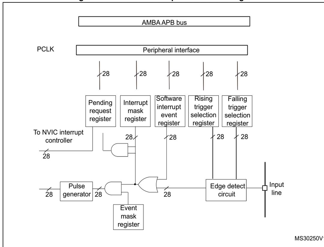
14.2.2 Block diagram
The extended interrupt/event block diagram is shown in the following figure.
Figure 50. External interrupt/event block diagram
14.2.3 Wake-up event management
STM32F3xx devices are able to handle external or internal events to wake up the core (WFE). The wake-up event can be generated either by:
- • enabling an interrupt in the peripheral control register but not in the NVIC, and enabling the SEVONPEND bit in the Cortex-M4 System Control register. When the MCU resumes from WFE, the EXTI peripheral interrupt pending bit and the peripheral NVIC IRQ channel pending bit (in the NVIC interrupt clear pending register) have to be cleared.
- • or by configuring an external or internal EXTI line in event mode. When the CPU resumes from WFE, it is not necessary to clear the peripheral interrupt pending bit or the NVIC IRQ channel pending bit as the pending bit corresponding to the event line is not set.
14.2.4 Asynchronous Internal Interrupts
Some communication peripherals (UART, I2C) are able to generate events when the system is in run mode and also when the system is in stop mode allowing to wake up the system from stop mode.
To accomplish this, the peripheral is asked to generate both a synchronized (to the system clock, for example, APB clock) and an asynchronous version of the event.
14.2.5 Functional description
For the external interrupt lines, to generate the interrupt, the interrupt line should be configured and enabled. This is done by programming the two trigger registers with the desired edge detection and by enabling the interrupt request by writing a '1' to the corresponding bit in the interrupt mask register. When the selected edge occurs on the external interrupt line, an interrupt request is generated. The pending bit corresponding to the interrupt line is also set. This request is reset by writing a 1 in the pending register.
For the internal interrupt lines, the active edge is always the rising edge. The interrupt is enabled by default in the interrupt mask register and there is no corresponding pending bit in the pending register.
To generate the event, the event line should be configured and enabled. This is done by programming the two trigger registers with the desired edge detection and by enabling the event request by writing a '1' to the corresponding bit in the event mask register. When the selected edge occurs on the event line, an event pulse is generated. The pending bit corresponding to the event line is not set.
For the external lines, an interrupt/event request can also be generated by software by writing a 1 in the software interrupt/event register.
Note: The interrupts or events associated to the internal lines can be triggered only when the system is in STOP mode. If the system is still running, no interrupt/event is generated.
Hardware interrupt selection
To configure a line as interrupt source, use the following procedure:
- • Configure the corresponding mask bit in the EXTI_IMR register.
- • Configure the Trigger Selection bits of the Interrupt line (EXTI_RTSR and EXTI_FTSR)
- • Configure the enable and mask bits that control the NVIC IRQ channel mapped to the EXTI so that an interrupt coming from one of the EXTI lines can be correctly acknowledged.
Hardware event selection
To configure a line as event source, use the following procedure:
- • Configure the corresponding mask bit in the EXTI_EMR register.
- • Configure the Trigger Selection bits of the Event line (EXTI_RTSR and EXTI_FTSR)
Software interrupt/event selection
Any of the external lines can be configured as software interrupt/event lines. The following is the procedure to generate a software interrupt.
- • Configure the corresponding mask bit (EXTI_IMR, EXTI_EMR)
- • Set the required bit of the software interrupt register (EXTI_SWIER)
14.2.6 External and internal interrupt/event line mapping
36 interrupt/event lines are available: 8 lines are internal (including the reserved ones); the remaining 28 lines are external.
The GPIOs are connected to the 16 external interrupt/event lines in the following manner:
Figure 51. External interrupt/event GPIO mapping
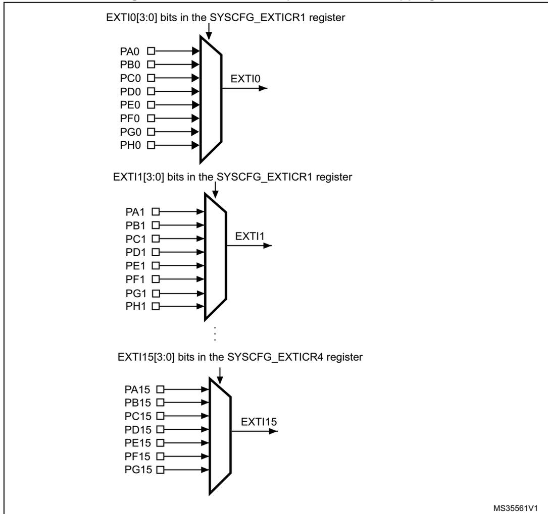
The diagram illustrates the mapping of GPIO pins to external interrupt lines. It consists of three multiplexer blocks, each controlled by a specific register bit field:
- EXTI0: Controlled by EXTI0[3:0] bits in the SYSCFG_EXTICR1 register . The multiplexer selects between PA0, PB0, PC0, PD0, PE0, PF0, PG0, and PH0.
- EXTI1: Controlled by EXTI1[3:0] bits in the SYSCFG_EXTICR1 register . The multiplexer selects between PA1, PB1, PC1, PD1, PE1, PF1, PG1, and PH1.
- EXTI15: Controlled by EXTI15[3:0] bits in the SYSCFG_EXTICR4 register . The multiplexer selects between PA15, PB15, PC15, PD15, PE15, PF15, and PG15.
Vertical ellipses between the EXTI1 and EXTI15 blocks indicate that the same pattern repeats for the remaining interrupt lines (EXTI2 through EXTI14). Each multiplexer has a single output line labeled with its corresponding EXTI number (e.g., EXTI0, EXTI1, EXTI15).
MS35561V1
The remaining lines are connected as follows:
- • EXTI line 16 is connected to the PVD output
- • EXTI line 17 is connected to the RTC Alarm event
- • EXTI line 18 is connected to USB Device FS wake-up event (STM32F303xB/C/D/E, STM32F358xC and STM32F398xE devices)
- • EXTI line 19 is connected to RTC tamper and timestamps
- • EXTI line 20 is connected to RTC wake-up timer
- • EXTI line 21 is connected to Comparator 1 output (STM32F303xB/C/D/E, STM32F358xC and STM32F398xE devices)
- • EXTI line 22 is connected to Comparator 2 output
- • EXTI line 23 is connected to I2C1 wake-up
- • EXTI line 24 is connected to I2C2 wake-up (STM32F303xB/C/D/E, STM32F358xC and STM32F398xE devices)
- • EXTI line 25 is connected to USART1 wake-up
- • EXTI line 26 is connected to USART2 wake-up (STM32F303xB/C/D/E, STM32F358xC and STM32F398xE devices)
- • EXTI line 27 is connected to I2C3 wake-up (STM32F303xD/E and STM32F398 devices)
- • EXTI line 28 is connected to USART3 wake-up (STM32F303xB/C/D/E, STM32F358xC and STM32F398xE devices)
- • EXTI line 29 is connected to Comparator 3 output (STM32F303xB/C/D/E, STM32F358xC and STM32F398xE devices)
- • EXTI line 30 is connected to Comparator 4 output
- • EXTI line 31 is connected to Comparator 5 output (STM32F303xB/C/D/E, STM32F358xC and STM32F398xE devices)
- • EXTI line 32 is connected to Comparator 6 output
- • EXTI line 33 is connected to Comparator 7 output (STM32F303xB/C/D/E, STM32F358xC and STM32F398xE devices)
- • EXTI line 34 is connected to UART4 wake-up (STM32F303xB/C/D/E, STM32F358xC and STM32F398xE devices)
- • EXTI line 35 is connected to UART5 wake-up (STM32F303xB/C/D/E, STM32F358xC and STM32F398xE devices)
Note: EXTI lines 23, 24, 25, 26, 27, 28, 34 and 35 are internal.
14.3 EXTI registers
Refer to Section 2.2 for a list of abbreviations used in register descriptions.
The peripheral registers have to be accessed by words (32-bit).
14.3.1 Interrupt mask register (EXTI_IMR1)
Address offset: 0x00
Reset value: 0x1F80 0000 (Refer to the note below)
| 31 | 30 | 29 | 28 | 27 | 26 | 25 | 24 | 23 | 22 | 21 | 20 | 19 | 18 | 17 | 16 |
|---|---|---|---|---|---|---|---|---|---|---|---|---|---|---|---|
| MR31 | MR30 | MR29 | MR28 | MR27 | MR26 | MR25 | MR24 | MR23 | MR22 | MR21 | MR20 | MR19 | MR18 | MR17 | MR16 |
| rw | rw | rw | rw | rw | rw | rw | rw | rw | rw | rw | rw | rw | rw | rw | rw |
| 15 | 14 | 13 | 12 | 11 | 10 | 9 | 8 | 7 | 6 | 5 | 4 | 3 | 2 | 1 | 0 |
|---|---|---|---|---|---|---|---|---|---|---|---|---|---|---|---|
| MR15 | MR14 | MR13 | MR12 | MR11 | MR10 | MR9 | MR8 | MR7 | MR6 | MR5 | MR4 | MR3 | MR2 | MR1 | MR0 |
| rw | rw | rw | rw | rw | rw | rw | rw | rw | rw | rw | rw | rw | rw | rw | rw |
Bits 31:0 MRx : Interrupt Mask on external/internal line x
0: Interrupt request from Line x is masked
1: Interrupt request from Line x is not masked
Note: The reset value for the internal lines (23, 24, 25, 26, 27 and 28) is set to '1' to enable the interrupt by default.
14.3.2 Event mask register (EXTI_EMR1)
Address offset: 0x04
Reset value: 0x0000 0000
| 31 | 30 | 29 | 28 | 27 | 26 | 25 | 24 | 23 | 22 | 21 | 20 | 19 | 18 | 17 | 16 |
|---|---|---|---|---|---|---|---|---|---|---|---|---|---|---|---|
| MR31 | MR30 | MR29 | MR28 | MR27 | MR26 | MR25 | MR24 | MR23 | MR22 | MR21 | MR20 | MR19 | MR18 | MR17 | MR16 |
| rw | rw | rw | rw | rw | rw | rw | rw | rw | rw | rw | rw | rw | rw | rw | rw |
| 15 | 14 | 13 | 12 | 11 | 10 | 9 | 8 | 7 | 6 | 5 | 4 | 3 | 2 | 1 | 0 |
|---|---|---|---|---|---|---|---|---|---|---|---|---|---|---|---|
| MR15 | MR14 | MR13 | MR12 | MR11 | MR10 | MR9 | MR8 | MR7 | MR6 | MR5 | MR4 | MR3 | MR2 | MR1 | MR0 |
| rw | rw | rw | rw | rw | rw | rw | rw | rw | rw | rw | rw | rw | rw | rw | rw |
Bits 31:0 MRx : Event Mask on external/internal line x
0: Event request from Line x is masked
1: Event request from Line x is not masked
14.3.3 Rising trigger selection register (EXTI_RTSR1)
Address offset: 0x08
Reset value: 0x0000 0000
| 31 | 30 | 29 | 28 | 27 | 26 | 25 | 24 | 23 | 22 | 21 | 20 | 19 | 18 | 17 | 16 |
| TR31 | TR30 | TR29 | Res. | Res. | Res. | Res. | Res. | Res. | TR22 | TR21 | TR20 | TR19 | TR18 | TR17 | TR16 |
| rw | rw | rw | rw | rw | rw | rw | rw | rw | rw | ||||||
| 15 | 14 | 13 | 12 | 11 | 10 | 9 | 8 | 7 | 6 | 5 | 4 | 3 | 2 | 1 | 0 |
| TR15 | TR14 | TR13 | TR12 | TR11 | TR10 | TR9 | TR8 | TR7 | TR6 | TR5 | TR4 | TR3 | TR2 | TR1 | TR0 |
| rw | rw | rw | rw | rw | rw | rw | rw | rw | rw | rw | rw | rw | rw | rw | rw |
Bits 31:29 TRx : Rising trigger event configuration bit of line x (x = 31 to 29)
0: Rising trigger disabled (for Event and Interrupt) for input line
1: Rising trigger enabled (for Event and Interrupt) for input line.
Bits 28:23 Reserved, must be kept at reset value.
Bits 22:0 TRx : Rising trigger event configuration bit of line x (x = 22 to 0)
0: Rising trigger disabled (for Event and Interrupt) for input line
1: Rising trigger enabled (for Event and Interrupt) for input line.
Note: The external wake-up lines are edge-triggered. No glitches must be generated on these lines. If a rising edge on an external interrupt line occurs during a write operation in the EXTI_RTSR register, the pending bit is not set.
Rising and falling edge triggers can be set for the same interrupt line. In this case, both generate a trigger condition.
14.3.4 Falling trigger selection register (EXTI_FTSR1)
Address offset: 0x0C
Reset value: 0x0000 0000
| 31 | 30 | 29 | 28 | 27 | 26 | 25 | 24 | 23 | 22 | 21 | 20 | 19 | 18 | 17 | 16 |
| TR31 | TR30 | TR29 | Res. | Res. | Res. | Res. | Res. | Res. | TR22 | TR21 | TR20 | TR19 | TR18 | TR17 | TR16 |
| rw | rw | rw | rw | rw | rw | rw | rw | rw | rw | ||||||
| 15 | 14 | 13 | 12 | 11 | 10 | 9 | 8 | 7 | 6 | 5 | 4 | 3 | 2 | 1 | 0 |
| TR15 | TR14 | TR13 | TR12 | TR11 | TR10 | TR9 | TR8 | TR7 | TR6 | TR5 | TR4 | TR3 | TR2 | TR1 | TR0 |
| rw | rw | rw | rw | rw | rw | rw | rw | rw | rw | rw | rw | rw | rw | rw | rw |
Bits 31:29 TRx : Falling trigger event configuration bit of line x (x = 31 to 29)
0: Falling trigger disabled (for Event and Interrupt) for input line
1: Falling trigger enabled (for Event and Interrupt) for input line.
Bits 28:23 Reserved, must be kept at reset value.
Bits 22:0 TRx : Falling trigger event configuration bit of line x (x = 22 to 0)
0: Falling trigger disabled (for Event and Interrupt) for input line
1: Falling trigger enabled (for Event and Interrupt) for input line.
Note: The external wake-up lines are edge-triggered. No glitches must be generated on these lines. If a falling edge on an external interrupt line occurs during a write operation to the EXTI_FTSR register, the pending bit is not set.
Rising and falling edge triggers can be set for the same interrupt line. In this case, both generate a trigger condition.
14.3.5 Software interrupt event register (EXTI_SWIER1)
Address offset: 0x10
Reset value: 0x0000 0000
| 31 | 30 | 29 | 28 | 27 | 26 | 25 | 24 | 23 | 22 | 21 | 20 | 19 | 18 | 17 | 16 |
|---|---|---|---|---|---|---|---|---|---|---|---|---|---|---|---|
| SWIER 31 | SWIER 30 | SWIER 29 | Res. | Res. | Res. | Res. | Res. | Res. | SWIER 22 | SWIER 21 | SWIER 20 | SWIER 19 | SWIER 18 | SWIER 17 | SWIER 16 |
| rw | rw | rw | rw | rw | rw | rw | rw | rw | rw |
| 15 | 14 | 13 | 12 | 11 | 10 | 9 | 8 | 7 | 6 | 5 | 4 | 3 | 2 | 1 | 0 |
|---|---|---|---|---|---|---|---|---|---|---|---|---|---|---|---|
| SWIER 15 | SWIER 14 | SWIER 13 | SWIER 12 | SWIER 11 | SWIER 10 | SWIER 9 | SWIER 8 | SWIER 7 | SWIER 6 | SWIER 5 | SWIER 4 | SWIER 3 | SWIER 2 | SWIER 1 | SWIER 0 |
| rw | rw | rw | rw | rw | rw | rw | rw | rw | rw | rw | rw | rw | rw | rw | rw |
Bits 31: 29 SWIERx : Software interrupt on line x (x = 31 to 29)
If the interrupt is enabled on this line in the EXTI_IMR, writing a '1' to this bit when it is at '0' sets the corresponding pending bit in EXTI_PR resulting in an interrupt request generation.
This bit is cleared by clearing the corresponding bit in the EXTI_PR register (by writing a '1' into the bit).
Bits 22:0 SWIERx : Software interrupt on line x (x = 22 to 0)
If the interrupt is enabled on this line in the EXTI_IMR, writing a '1' to this bit when it is at '0' sets the corresponding pending bit in EXTI_PR resulting in an interrupt request generation.
This bit is cleared by clearing the corresponding bit of EXTI_PR (by writing a '1' into the bit).
14.3.6 Pending register (EXTI_PR1)
Address offset: 0x14
Reset value: 0x0000 0000
| 31 | 30 | 29 | 28 | 27 | 26 | 25 | 24 | 23 | 22 | 21 | 20 | 19 | 18 | 17 | 16 |
|---|---|---|---|---|---|---|---|---|---|---|---|---|---|---|---|
| PR31 | PR30 | PR29 | Res. | Res. | Res. | Res. | Res. | Res. | PR22 | PR21 | PR20 | PR19 | PR18 | PR17 | PR16 |
| rc_w1 | rc_w1 | rc_w1 | rc_w1 | rc_w1 | rc_w1 | rc_w1 | rc_w1 | rc_w1 | rc_w1 |
| 15 | 14 | 13 | 12 | 11 | 10 | 9 | 8 | 7 | 6 | 5 | 4 | 3 | 2 | 1 | 0 |
|---|---|---|---|---|---|---|---|---|---|---|---|---|---|---|---|
| PR15 | PR14 | PR13 | PR12 | PR11 | PR10 | PR9 | PR8 | PR7 | PR6 | PR5 | PR4 | PR3 | PR2 | PR1 | PR0 |
| rc_w1 | rc_w1 | rc_w1 | rc_w1 | rc_w1 | rc_w1 | rc_w1 | rc_w1 | rc_w1 | rc_w1 | rc_w1 | rc_w1 | rc_w1 | rc_w1 | rc_w1 | rc_w1 |
Bits 31:29 PRx : Pending bit on line x (x = 31 to 29)
0: No trigger request occurred
1: Selected trigger request occurred
This bit is set when the selected edge event arrives on the external interrupt line.
This bit is cleared by writing a '1' to the bit.
Bits 28:23 Reserved, must be kept at reset value.
Bits 22:0 PRx : Pending bit on line x (x = 22 to 0)
0: No trigger request occurred
1: Selected trigger request occurred
This bit is set when the selected edge event arrives on the external interrupt line.
This bit is cleared by writing a '1' to the bit.
14.3.7 Interrupt mask register (EXTI_IMR2)
Address offset: 0x20
Reset value: 0xFFFF FFFC (See note below)
| 31 | 30 | 29 | 28 | 27 | 26 | 25 | 24 | 23 | 22 | 21 | 20 | 19 | 18 | 17 | 16 |
|---|---|---|---|---|---|---|---|---|---|---|---|---|---|---|---|
| Res. | Res. | Res. | Res. | Res. | Res. | Res. | Res. | Res. | Res. | Res. | Res. | Res. | Res. | Res. | Res. |
| 15 | 14 | 13 | 12 | 11 | 10 | 9 | 8 | 7 | 6 | 5 | 4 | 3 | 2 | 1 | 0 |
| Res. | Res. | Res. | Res. | Res. | Res. | Res. | Res. | Res. | Res. | Res. | Res. | MR35 | MR34 | MR33 | MR32 |
| rw | rw | rw | rw |
Bits 31:4 Reserved, must be kept at reset value
Bits 3:0 MRx : Interrupt mask on external/internal line x, x = 32..35
0: Interrupt request from Line x is masked
1: Interrupt request from Line x is not masked
Note: The reset value for the internal lines (34 and 35) and reserved lines is set to '1'.
14.3.8 Event mask register (EXTI_EMR2)
Address offset: 0x24
Reset value: 0x0000 0000
| 31 | 30 | 29 | 28 | 27 | 26 | 25 | 24 | 23 | 22 | 21 | 20 | 19 | 18 | 17 | 16 |
|---|---|---|---|---|---|---|---|---|---|---|---|---|---|---|---|
| Res. | Res. | Res. | Res. | Res. | Res. | Res. | Res. | Res. | Res. | Res. | Res. | Res. | Res. | Res. | Res. |
| 15 | 14 | 13 | 12 | 11 | 10 | 9 | 8 | 7 | 6 | 5 | 4 | 3 | 2 | 1 | 0 |
| Res. | Res. | Res. | Res. | Res. | Res. | Res. | Res. | Res. | Res. | Res. | Res. | MR35 | MR34 | MR33 | MR32 |
| rw | rw | rw | rw |
Bits 31:4 Reserved, must be kept at reset value
Bits 3:0 MRx : Event mask on external/internal line x, x = 32..35
0: Event request from Line x is masked
1: Event request from Line x is not masked
14.3.9 Rising trigger selection register (EXTI_RTSR2)
Address offset: 0x28
Reset value: 0x0000 0000
| 31 | 30 | 29 | 28 | 27 | 26 | 25 | 24 | 23 | 22 | 21 | 20 | 19 | 18 | 17 | 16 |
|---|---|---|---|---|---|---|---|---|---|---|---|---|---|---|---|
| Res. | Res. | Res. | Res. | Res. | Res. | Res. | Res. | Res. | Res. | Res. | Res. | Res. | Res. | Res. | Res. |
| 15 | 14 | 13 | 12 | 11 | 10 | 9 | 8 | 7 | 6 | 5 | 4 | 3 | 2 | 1 | 0 |
| Res. | Res. | Res. | Res. | Res. | Res. | Res. | Res. | Res. | Res. | Res. | Res. | Res. | Res. | TR33 | TR32 |
| rw | rw |
Bits 31:2 Reserved, must be kept at reset value.
Bits 1:0 TRx : Rising trigger event configuration bit of line x (x = 32, 33)
0: Rising trigger disabled (for Event and Interrupt) for input line
1: Rising trigger enabled (for Event and Interrupt) for input line.
Note: The external wake-up lines are edge-triggered. No glitches must be generated on these lines. If a rising edge on an external interrupt line occurs during a write operation to the EXTI_RTSR register, the pending bit is not set.
Rising and falling edge triggers can be set for the same interrupt line. In this case, both generate a trigger condition.
14.3.10 Falling trigger selection register (EXTI_FTSR2)
Address offset: 0x2C
Reset value: 0x0000 0000
| 31 | 30 | 29 | 28 | 27 | 26 | 25 | 24 | 23 | 22 | 21 | 20 | 19 | 18 | 17 | 16 |
|---|---|---|---|---|---|---|---|---|---|---|---|---|---|---|---|
| Res. | Res. | Res. | Res. | Res. | Res. | Res. | Res. | Res. | Res. | Res. | Res. | Res. | Res. | Res. | Res. |
| 15 | 14 | 13 | 12 | 11 | 10 | 9 | 8 | 7 | 6 | 5 | 4 | 3 | 2 | 1 | 0 |
| Res. | Res. | Res. | Res. | Res. | Res. | Res. | Res. | Res. | Res. | Res. | Res. | Res. | Res. | TR33 | TR32 |
| rw | rw |
Bits 31:2 Reserved, must be kept at reset value.
Bits 1:0 TRx : Falling trigger event configuration bit of line x (x = 32, 33)
0: Falling trigger disabled (for Event and Interrupt) for input line
1: Falling trigger enabled (for Event and Interrupt) for input line.
Note: The external wake-up lines are edge-triggered. No glitches must be generated on these lines. If a falling edge on an external interrupt line occurs during a write operation to the EXTI_FTSR register, the pending bit is not set.
Rising and falling edge triggers can be set for the same interrupt line. In this case, both generate a trigger condition.
14.3.11 Software interrupt event register (EXTI_SWIER2)
Address offset: 0x30
Reset value: 0x0000 0000
| 31 | 30 | 29 | 28 | 27 | 26 | 25 | 24 | 23 | 22 | 21 | 20 | 19 | 18 | 17 | 16 |
|---|---|---|---|---|---|---|---|---|---|---|---|---|---|---|---|
| Res. | Res. | Res. | Res. | Res. | Res. | Res. | Res. | Res. | Res. | Res. | Res. | Res. | Res. | Res. | Res. |
| 15 | 14 | 13 | 12 | 11 | 10 | 9 | 8 | 7 | 6 | 5 | 4 | 3 | 2 | 1 | 0 |
| Res. | Res. | Res. | Res. | Res. | Res. | Res. | Res. | Res. | Res. | Res. | Res. | Res. | Res. | SWIER 33 | SWIER 32 |
| rw | rw |
Bits 31:2 Reserved, must be kept at reset value.
Bits 1:0 SWIERx : Software interrupt on line x (x = 32, 33)
If the interrupt is enabled on this line in the EXTI_IMR , writing a '1' to this bit when it is at '0' sets the corresponding pending bit in EXTI_PR resulting in an interrupt request generation.
This bit is cleared by clearing the corresponding bit of EXTI_PR (by writing a '1' to the bit).
14.3.12 Pending register (EXTI_PR2)
Address offset: 0x34
Reset value: 0x0000 0000
| 31 | 30 | 29 | 28 | 27 | 26 | 25 | 24 | 23 | 22 | 21 | 20 | 19 | 18 | 17 | 16 |
|---|---|---|---|---|---|---|---|---|---|---|---|---|---|---|---|
| Res. | Res. | Res. | Res. | Res. | Res. | Res. | Res. | Res. | Res. | Res. | Res. | Res. | Res. | Res. | Res. |
| 15 | 14 | 13 | 12 | 11 | 10 | 9 | 8 | 7 | 6 | 5 | 4 | 3 | 2 | 1 | 0 |
| Res. | Res. | Res. | Res. | Res. | Res. | Res. | Res. | Res. | Res. | Res. | Res. | Res. | Res. | PR33 | PR32 |
| rc_w1 | rc_w1 |
Bits 31:2 Reserved, must be kept at reset value.
Bits 1:0 PRx : Pending bit on line x (x = 32,33)
0: No trigger request occurred
1: Selected trigger request occurred
This bit is set when the selected edge event arrives on the external interrupt line.
This bit is cleared by writing a '1' into the bit.
14.3.13 EXTI register map
Table 84. External interrupt/event controller register map and reset values
| Offset | Register | 31 | 30 | 29 | 28 | 27 | 26 | 25 | 24 | 23 | 22 | 21 | 20 | 19 | 18 | 17 | 16 | 15 | 14 | 13 | 12 | 11 | 10 | 9 | 8 | 7 | 6 | 5 | 4 | 3 | 2 | 1 | 0 |
|---|---|---|---|---|---|---|---|---|---|---|---|---|---|---|---|---|---|---|---|---|---|---|---|---|---|---|---|---|---|---|---|---|---|
| 0x00 | EXTI_IMR1 | MR[31:0] | |||||||||||||||||||||||||||||||
| Reset value | 0 | 0 | 0 | 1 | 1 | 1 | 1 | 1 | 1 | 0 | 0 | 0 | 0 | 0 | 0 | 0 | 0 | 0 | 0 | 0 | 0 | 0 | 0 | 0 | 0 | 0 | 0 | 0 | 0 | ||||
| 0x04 | EXTI_EMR1 | MR[31:0] | |||||||||||||||||||||||||||||||
| Reset value | 0 | 0 | 0 | 0 | 0 | 0 | 0 | 0 | 0 | 0 | 0 | 0 | 0 | 0 | 0 | 0 | 0 | 0 | 0 | 0 | 0 | 0 | 0 | 0 | 0 | 0 | 0 | 0 | 0 | 0 | 0 | ||
| 0x08 | EXTI_RTSR1 | TR[31:29] | Res. | Res. | Res. | Res. | Res. | Res. | TR[22:0] | ||||||||||||||||||||||||
| Reset value | 0 | 0 | 0 | 0 | 0 | 0 | 0 | 0 | 0 | 0 | 0 | 0 | 0 | 0 | 0 | 0 | 0 | 0 | 0 | 0 | 0 | 0 | 0 | 0 | 0 | ||||||||
| 0x0C | EXTI_FTSR1 | TR[31:29] | Res. | Res. | Res. | Res. | Res. | Res. | TR[22:0] | ||||||||||||||||||||||||
| Reset value | 0 | 0 | 0 | 0 | 0 | 0 | 0 | 0 | 0 | 0 | 0 | 0 | 0 | 0 | 0 | 0 | 0 | 0 | 0 | 0 | 0 | 0 | 0 | 0 | 0 | ||||||||
| 0x10 | EXTI_SWIER1 | SWIER[31:29] | Res. | Res. | Res. | Res. | Res. | Res. | SWIER[22:0] | ||||||||||||||||||||||||
| Reset value | 0 | 0 | 0 | 0 | 0 | 0 | 0 | 0 | 0 | 0 | 0 | 0 | 0 | 0 | 0 | 0 | 0 | 0 | 0 | 0 | 0 | 0 | 0 | 0 | 0 | ||||||||
| 0x14 | EXTI_PR1 | PR[31:29] | Res. | Res. | Res. | Res. | Res. | Res. | PR[22:0] | ||||||||||||||||||||||||
| Reset value | 0 | 0 | 0 | 0 | 0 | 0 | 0 | 0 | 0 | 0 | 0 | 0 | 0 | 0 | 0 | 0 | 0 | 0 | 0 | 0 | 0 | 0 | 0 | 0 | 0 | ||||||||
| 0x20 | EXTI_IMR2 | Res. | Res. | Res. | Res. | Res. | Res. | Res. | Res. | Res. | Res. | Res. | Res. | Res. | Res. | Res. | Res. | Res. | Res. | Res. | Res. | Res. | Res. | Res. | Res. | Res. | Res. | Res. | Res. | MR35 | MR34 | MR33 | MR32 |
| Reset value | 1 | 1 | 0 | 0 | |||||||||||||||||||||||||||||
| 0x24 | EXTI_EMR2 | Res. | Res. | Res. | Res. | Res. | Res. | Res. | Res. | Res. | Res. | Res. | Res. | Res. | Res. | Res. | Res. | Res. | Res. | Res. | Res. | Res. | Res. | Res. | Res. | Res. | Res. | Res. | Res. | MR35 | MR34 | MR33 | MR32 |
| Reset value | 0 | 0 | 0 | 0 | |||||||||||||||||||||||||||||
| 0x28 | EXTI_RTSR2 | Res. | Res. | Res. | Res. | Res. | Res. | Res. | Res. | Res. | Res. | Res. | Res. | Res. | Res. | Res. | Res. | Res. | Res. | Res. | Res. | Res. | Res. | Res. | Res. | Res. | Res. | Res. | Res. | Res. | Res. | TR33 | TR32 |
| Reset value | 0 | 0 | |||||||||||||||||||||||||||||||
| 0x2C | EXTI_FTSR2 | Res. | Res. | Res. | Res. | Res. | Res. | Res. | Res. | Res. | Res. | Res. | Res. | Res. | Res. | Res. | Res. | Res. | Res. | Res. | Res. | Res. | Res. | Res. | Res. | Res. | Res. | Res. | Res. | Res. | Res. | TR33 | TR32 |
| Reset value | 0 | 0 | |||||||||||||||||||||||||||||||
| 0x30 | EXTI_SWIER2 | Res. | Res. | Res. | Res. | Res. | Res. | Res. | Res. | Res. | Res. | Res. | Res. | Res. | Res. | Res. | Res. | Res. | Res. | Res. | Res. | Res. | Res. | Res. | Res. | Res. | Res. | Res. | Res. | Res. | Res. | SWIER33 | SWIER32 |
| Reset value | 0 | 0 | |||||||||||||||||||||||||||||||
| 0x34 | EXTI_PR2 | Res. | Res. | Res. | Res. | Res. | Res. | Res. | Res. | Res. | Res. | Res. | Res. | Res. | Res. | Res. | Res. | Res. | Res. | Res. | Res. | Res. | Res. | Res. | Res. | Res. | Res. | Res. | Res. | Res. | Res. | PR33 | PR32 |
| Reset value | 0 | 0 | |||||||||||||||||||||||||||||||