13. Direct memory access controller (DMA)
13.1 Introduction
The direct memory access (DMA) controller is a bus master and system peripheral.
The DMA is used to perform programmable data transfers between memory-mapped peripherals and/or memories, upon the control of an off-loaded CPU.
The DMA controller features a single AHB master architecture.
There is one instance of DMA with up to 7 channels, except for the STM32F303xB/C/D/E, STM32F358xC and STM32F398xCE devices that also include a DMA2 with 5 channels.
Each channel is dedicated to managing memory access requests from one or more peripherals. Each DMA includes an arbiter for handling the priority between DMA requests.
13.2 DMA main features
- • Single AHB master
- • Peripheral-to-memory, memory-to-peripheral, memory-to-memory and peripheral-to-peripheral data transfers
- • Access, as source and destination, to on-chip memory-mapped devices such as flash memory, SRAM, and AHB and APB peripherals
- • All DMA channels independently configurable:
- – Each channel is associated either with a DMA request signal coming from a peripheral, or with a software trigger in memory-to-memory transfers. This configuration is done by software.
- – Priority between the requests is programmable by software (four levels per channel: very high, high, medium, low) and by hardware in case of equality (such as request to channel 1 has priority over request to channel 2).
- – Transfer size of source and destination are independent (byte, half-word, word), emulating packing and unpacking. Source and destination addresses must be aligned on the data size.
- – Support of transfers from/to peripherals to/from memory with circular buffer management
- – Programmable number of data to be transferred: 0 to \( 2^{16} - 1 \)
- • Generation of an interrupt request per channel. Each interrupt request is caused from any of the three DMA events: transfer complete, half transfer, or transfer error.
13.3 DMA implementation
13.3.1 DMA1 and DMA2
DMA1 and DMA2 are implemented with the hardware configuration parameters shown in the table below.
Table 75. DMA1 and DMA2 implementation
| Feature | DMA1 | DMA2 |
|---|---|---|
| Number of channels | 7 | 5 (1) |
1. DMA2 only for STM32F303xB/C/D/E, STM32F358xC and STM32F398xCE devices.
13.3.2 DMA request mapping
DMA1 controller
The hardware requests from the peripherals (TIMx(x=1...4, 6, 7, 15..17), ADC1, ADC2, SPI1, SPI2/I2S, I2Cx(x=1,2), DAC1_Channel[1,2], DAC2_Channel[1] and USARTx (x=1..3)) are simply logically ORed before entering the DMA. This means that on one channel, only one request must be enabled at a time (see Figure 46 and Figure 47 ).
The peripheral DMA requests can be independently activated/de-activated by programming the DMA control bit in the registers of the corresponding peripheral.
Caution: A same peripheral request can be assigned to two different channels only if the application ensures that these channels are not requested to be served at the same time. In other words, if two different channels receive a same asserted peripheral request at the same time, an unpredictable DMA hardware behavior occurs.
Table 76 and Table 77 list the DMA requests for each channel.
Figure 46. DMA1 request mapping on STM32F303xB/C/D/E, STM32F358xC and STM32F398xE devices
| Peripheral request signals | DMA | Fixed hardware priority |
|---|---|---|
| ADC1 TIM2_CH3 TIM4_CH1 TIM17_CH1 TIM17_UP | HW request 1 SW trigger 1 (MEM2MEM bit) → OR gate → Channel 1 | High priority ↓ Internal DMA request ↓ Low priority |
| SPI1_RX USART3_TX TIM1_CH1 TIM2_UP TIM3_CH3 | HW request 2 SW trigger 2 (MEM2MEM bit) → OR gate → Channel 2 | |
| SPI1_TX USART3_RX TIM1_CH2 TIM3_CH4 TIM3_UP TIM6_UP DAC_CH1 (1) TIM16_CH1 TIM16_UP | HW request 3 SW trigger 3 (MEM2MEM bit) → OR gate → Channel 3 | |
| SPI2_RX USART1_TX I2C2_TX TIM1_CH4 TIM1_TRIG TIM1_COM TIM4_CH2 TIM7_UP DAC_CH2 (1) | HW request 4 SW trigger 4 (MEM2MEM bit) → OR gate → Channel 4 | |
| SPI2_TX USART1_RX I2C2_RX TIM1_UP TIM2_CH1 TIM4_CH3 TIM15_CH1 TIM15_UP TIM15_TRIG TIM15_COM | HW request 5 SW trigger 5 (MEM2MEM bit) → OR gate → Channel 5 | |
| USART2_RX I2C1_TX TIM1_CH3 TIM3_CH1 TIM3_TRIG TIM16_CH1 TIM16_UP (1) | HW request 6 SW trigger 6 (MEM2MEM bit) → OR gate → Channel 6 | |
| USART2_TX I2C1_RX TIM2_CH2 TIM2_CH4 TIM4_UP TIM17_CH1 TIM17_UP (1) | HW request 7 SW trigger 7 (MEM2MEM bit) → OR gate → Channel 7 |
MS30228V1
1. DMA request mapped on this DMA channel only if the corresponding remapping bit is set in SYSCFG configuration register 1 (SYSCFG_CFGR1) .
Figure 47. DMA1 request mapping on STM32F303x6/8 and STM32F328x8 devices
The diagram illustrates the mapping of peripheral request signals to DMA1 channels. It is organized into three main columns: 'Peripheral request signals', 'DMA', and 'Fixed hardware priority'.
- Peripheral request signals:
Lists various peripherals and their specific request lines. Some are grouped by an OR gate leading to a DMA 'HW request' line.
- ADC1, TIM2_CH3, TIM17_CH1, TIM17_UP → HW request 1
- SPI1_RX, USART3_TX, TIM1_CH1, TIM2_UP, TIM3_CH3, ADC2, I2C1_TX → HW request 2
- SPI1_TX, USART3_RX, TIM1_CH2, TIM6_UP, DAC1_CH1, TIM16_CH1, TIM16_UP (1) , I2C1_RX → HW request 3
- SPI1_RX, USART1_TX, I2C1_TX, TIM1_CH4, TIM1_TRIG, TIM1_COM, TIM7_UP, DAC1_CH2 (1) , ADC2 → HW request 4
- SPI1_TX (2) , USART1_RX, I2C1_RX, TIM1_UP, TIM2_CH1, DAC2_CH1, TIM15_CH1, TIM15_UP, TIM15_TRIG, TIM15_COM → HW request 5
- USART2_RX, I2C1_TX, TIM1_CH3, TIM3_CH1, TIM3_TRIG, TIM16_CH1, TIM16_UP (1) , SPI1_RX → HW request 6
- USART2_TX, I2C1_RX, TIM2_CH2, TIM2_CH4, TIM17_CH1, TIM17_UP (1) , SPI1_TX → HW request 7
- DMA: Each 'HW request' line connects to an OR gate. Each OR gate also receives a 'SW trigger' input (labeled 'SW trigger n (MEM2MEM bit)'). The output of each OR gate is a 'Channel' line (Channel1 through Channel7).
- Fixed hardware priority: A vertical bar on the right indicates priority, with 'High priority' at the top (Channel 1) and 'Low priority' at the bottom (Channel 7). An arrow points from the 'Internal DMA request' block down this priority bar.
MS32643V1
1. DMA request mapped on this DMA channel only if the corresponding remapping bit is set in SYSCFG configuration register 1 (SYSCFG_CFGR1) and SYSCFG configuration register 3 (SYSCFG_CFGR3) .
2. SPI1_TX_DMA_RMP[1:0] bits in SYSCFG configuration register 2 (SYSCFG_CFGR2) allow remapping of SPI1_TX on channel 5 and 7.
Table 76. DMA1 requests for each channel on STM32F303xB/C/D/E, STM32F358xC and STM32F398xE devices
| Peripheral | Channel 1 | Channel 2 | Channel 3 | Channel 4 | Channel 5 | Channel 6 | Channel 7 |
|---|---|---|---|---|---|---|---|
| ADC | ADC1 | - | - | - | - | - | - |
| SPI | - | SPI1_RX | SPI1_TX | SPI2_RX | SPI2_TX | - | - |
| USART | - | USART3_TX | USART3_RX | USART1_TX | USART1_RX | USART2_RX | USART2_TX |
| I2C | I2C3_TX (1) | I2C3_RX (1) | - | I2C2_TX | I2C2_RX | I2C1_TX | I2C1_RX |
| TIM1 | - | TIM1_CH1 | TIM1_CH2 | TIM1_CH4 TIM1_TRIG TIM1_COM | TIM1_UP | TIM1_CH3 | - |
| TIM2 | TIM2_CH3 | TIM2_UP | - | - | TIM2_CH1 | - | TIM2_CH2 TIM2_CH4 |
| TIM3 | - | TIM3_CH3 | TIM3_CH4 TIM3_UP | - | - | TIM3_CH1 TIM3_TRIG | - |
| TIM4 | TIM4_CH1 | - | - | TIM4_CH2 | TIM4_CH3 | - | TIM4_UP |
| TIM6 / DAC | - | - | TIM6_UP DAC_CH1 (2) | - | - | - | - |
| TIM7/DAC | - | - | - | TIM7_UP DAC_CH2 (2) | - | - | - |
| TIM15 | - | - | - | - | TIM15_CH1 TIM15_UP TIM15_TRIG TIM15_COM | - | - |
| TIM16 | - | - | TIM16_CH1 TIM16_UP | - | - | TIM16_CH1 TIM16_UP (2) | - |
| TIM17 | TIM17_CH1 TIM17_UP | - | - | - | - | - | TIM17_CH1 TIM17_UP (2) |
1. Available in STM32F303xD/E only.
2. DMA request mapped on this DMA channel only if the corresponding remapping bit is set in SYSCFG configuration register 1 (SYSCFG_CFGR1) .
Table 77. DMA1 requests for each channel on STM32F303x6/8 and STM32F328x8 devices
| Peripheral | Channel 1 | Channel 2 | Channel 3 | Channel 4 | Channel 5 | Channel 6 | Channel 7 |
|---|---|---|---|---|---|---|---|
| ADC | ADC1 | ADC2 | - | ADC2 (1) | - | - | - |
| SPI | - | SPI1_RX | SPI1_TX | SPI1_RX (1) | SPI1_TX (1) | SPI1_RX (1) | SPI1_TX (1) |
| USART | - | USART3_TX | USART3_RX | USART1_TX | USART1_RX | USART2_RX | USART2_TX |
| I2C | - | I2C1_TX (1) | I2C1_RX (1) | I2C1_TX (1) | I2C1_RX (1) | I2C1_TX | I2C1_RX |
| TIM1 | - | TIM1_CH1 | TIM1_CH2 | TIM1_CH4 TIM1_TRIG TIM1_COM | TIM1_UP | TIM1_CH3 | - |
| TIM2 | TIM2_CH3 | TIM2_UP | - | - | TIM2_CH1 | - | TIM2_CH2 TIM2_CH4 |
Table 77. DMA1 requests for each channel on STM32F303x6/8 and STM32F328x8 devices (continued)
| Peripheral | Channel 1 | Channel 2 | Channel 3 | Channel 4 | Channel 5 | Channel 6 | Channel 7 |
|---|---|---|---|---|---|---|---|
| TIM3 | - | TIM3_CH3 | TIM3_CH4 TIM3_UP | - | - | TIM3_CH1 TIM3_TRIG | - |
| TIM6/DAC | - | - | TIM6_UP DAC1_CH1 (1) | - | - | - | - |
| TIM7/DAC | - | - | - | TIM7_UP DAC2_CH2 (1) | - | - | - |
| DAC | - | - | - | - | DAC2_CH1 (1) | - | - |
| TIM15 | - | - | - | - | TIM15_CH1 TIM15_UP TIM15_TRIG TIM15_COM | - | - |
| TIM16 | - | - | TIM16_CH1 TIM16_UP | - | - | TIM16_CH1 TIM16_UP (1) | - |
| TIM17 | TIM17_CH1 TIM17_UP | - | - | - | - | - | TIM17_CH1 TIM17_UP (1) |
- 1. DMA request mapped on this DMA channel only if the corresponding remapping bit is set in SYSCFG configuration register 1 (SYSCFG_CFGR1) and SYSCFG configuration register 3 (SYSCFG_CFGR3) .
DMA2 controller
The hardware requests from the peripherals (TIMx (x = 6,7,8), ADCx (x = 2,3,4), SPI/I2S3, UART4, DAC_Channel[1,2]) are simply logically ORed before entering the DMA. This means that on one channel, only one request must be enabled at a time (see Figure 48 ).
The peripheral DMA requests can be independently activated/de-activated by programming the DMA control bit in the registers of the corresponding peripheral.
Caution: A same peripheral request can be assigned to two different channels only if the application ensures that these channels are not requested to be served at the same time. In other words, if two different channels receive a same asserted peripheral request at the same time, an unpredictable DMA hardware behavior occurs.
Table 78 lists the DMA requests for each channel.
Figure 48. DMA2 request mapping on STM32F303xB/C/D/E, STM32F358xC and STM32F398xE devices
The diagram illustrates the DMA2 request mapping for five channels. Each channel is associated with specific peripheral request signals and a software trigger. The hardware requests are derived from the following signals:
- Channel 1: ADC2, SPI3_RX, TIM8_CH3, TIM8_UP.
- Channel 2: ADC4, SPI3_TX, TIM8_CH4, TIM8_TRIG, TIM8_COM.
- Channel 3: ADC2 (1) , UART4_RX, TIM6_UP, DAC_CH1, TIM8_CH1.
- Channel 4: ADC4 (1) , TIM7_UP, DAC_CH2.
- Channel 5: ADC3, UART4_TX, TIM8_CH2.
Each channel has a hardware request (HW request) and a software trigger (SW trigger) input. The software triggers are derived from the MEM2MEM bit. The channels are prioritized from High priority (Channel 1) to Low priority (Channel 5). Channel 3 and Channel 4 have an additional internal DMA request output.
MS30229V1
1. DMA request mapped on this DMA channel only if the corresponding remapping bit is set in SYSCFG configuration register 1 (SYSCFG_CFGR1) .
Table 78. DMA2 requests for each channel on STM32F303xB/C/D/E, STM32F358xC and STM32F398xE devices
| Peripheral | Channel 1 | Channel 2 | Channel 3 | Channel 4 | Channel 5 |
|---|---|---|---|---|---|
| ADC | ADC2 | ADC4 | ADC2 (1) | ADC4 (1) | ADC3 |
| SPI | SPI3_RX | SPI3_TX | - | SPI4_RX (2) | SPI4_TX (2) |
| UART4 | - | - | UART4_RX | - | UART4_TX |
Table 78. DMA2 requests for each channel on STM32F303xB/C/D/E, STM32F358xC and STM32F398xE devices (continued)
| Peripheral | Channel 1 | Channel 2 | Channel 3 | Channel 4 | Channel 5 |
|---|---|---|---|---|---|
| TIM6/DAC | - | - | TIM6_UP DAC_CH1 | - | - |
| TIM7/DAC | - | - | - | TIM7_UP DAC_CH2 | - |
| TIM8 | TIM8_CH3 TIM8_UP | TIM8_CH4 TIM8_TRIG TIM8_COM | TIM8_CH1 | - | TIM8_CH2 |
| TIM20 (2) | TIM20_CH1 | TIM20_CH2 | TIM20_CH3 TIM20_UP | TIM20_CH4 TIM20_TRIG TIM20_COM | - |
1. DMA request mapped on this DMA channel only if the corresponding remapping bit is set in SYSCFG configuration register 1 (SYSCFG_CFGR1) .
2. Available in STM32F303xD/E only.
13.4 DMA functional description
13.4.1 DMA block diagram
The DMA block diagram is shown in the figure below.
Figure 49. DMA block diagram
The DMA controller performs direct memory transfer by sharing the AHB system bus with other system masters. The bus matrix implements round-robin scheduling. DMA requests may stop the CPU access to the system bus for a number of bus cycles, when CPU and DMA target the same destination (memory or peripheral).
According to its configuration through the AHB slave interface, the DMA controller arbitrates between the DMA channels and their associated received requests. The DMA controller also schedules the DMA data transfers over the single AHB port master.
The DMA controller generates an interrupt per channel to the interrupt controller.
13.4.2 DMA transfers
The software configures the DMA controller at channel level, in order to perform a block transfer, composed of a sequence of AHB bus transfers.
A DMA block transfer may be requested from a peripheral, or triggered by the software in case of memory-to-memory transfer.
After an event, the following steps of a single DMA transfer occur:
- 1. The peripheral sends a single DMA request signal to the DMA controller.
- 2. The DMA controller serves the request, depending on the priority of the channel associated to this peripheral request.
- 3. As soon as the DMA controller grants the peripheral, an acknowledge is sent to the peripheral by the DMA controller.
- 4. The peripheral releases its request as soon as it gets the acknowledge from the DMA controller.
- 5. Once the request is de-asserted by the peripheral, the DMA controller releases the acknowledge.
The peripheral may order a further single request and initiate another single DMA transfer.
The request/acknowledge protocol is used when a peripheral is either the source or the destination of the transfer. For example, in case of memory-to-peripheral transfer, the peripheral initiates the transfer by driving its single request signal to the DMA controller. The DMA controller reads then a single data in the memory and writes this data to the peripheral.
For a given channel x, a DMA block transfer consists of a repeated sequence of:
- • a single DMA transfer, encapsulating two AHB transfers of a single data, over the DMA AHB bus master:
- – a single data read (byte, half-word, or word) from the peripheral data register or a location in the memory, addressed through an internal current peripheral/memory address register.
The start address used for the first single transfer is the base address of the peripheral or memory, and is programmed in the DMA_CPARx or DMA_CMARx register. - – a single data write (byte, half-word, or word) to the peripheral data register or a location in the memory, addressed through an internal current peripheral/memory address register.
The start address used for the first transfer is the base address of the peripheral or memory, and is programmed in the DMA_CPARx or DMA_CMARx register.
- – a single data read (byte, half-word, or word) from the peripheral data register or a location in the memory, addressed through an internal current peripheral/memory address register.
- • post-decrementing of the programmed DMA_CNDTRx register
This register contains the remaining number of data items to transfer (number of AHB 'read followed by write' transfers).
This sequence is repeated until DMA_CNDTRx is null.
Note: The AHB master bus source/destination address must be aligned with the programmed size of the transferred single data to the source/destination.
13.4.3 DMA arbitration
The DMA arbiter manages the priority between the different channels.
When an active channel x is granted by the arbiter (hardware requested or software triggered), a single DMA transfer is issued (such as a AHB 'read followed by write' transfer of a single data). Then, the arbiter considers again the set of active channels and selects the one with the highest priority.
The priorities are managed in two stages:
- • software: priority of each channel is configured in the DMA_CCRx register, to one of the four different levels:
- – very high
- – high
- – medium
- – low
- • hardware: if two requests have the same software priority level, the channel with the lowest index gets priority. For example, channel 2 gets priority over channel 4.
When a channel x is programmed for a block transfer in memory-to-memory mode, re arbitration is considered between each single DMA transfer of this channel x. Whenever there is another concurrent active requested channel, the DMA arbiter automatically alternates and grants the other highest-priority requested channel, which may be of lower priority than the memory-to-memory channel.
13.4.4 DMA channels
Each channel may handle a DMA transfer between a peripheral register located at a fixed address, and a memory address. The amount of data items to transfer is programmable. The register that contains the amount of data items to transfer is decremented after each transfer.
A DMA channel is programmed at block transfer level.
Programmable data sizes
The transfer sizes of a single data (byte, half-word, or word) to the peripheral and memory are programmable through, respectively, the PSIZE[1:0] and MSIZE[1:0] fields of the DMA_CCRx register.
Pointer incrementation
The peripheral and memory pointers may be automatically incremented after each transfer, depending on the PINC and MINC bits of the DMA_CCRx register.
If the incremented mode is enabled (PINC or MINC set to 1), the address of the next transfer is the address of the previous one incremented by 1, 2 or 4, depending on the data size defined in PSIZE[1:0] or MSIZE[1:0]. The first transfer address is the one programmed in the DMA_CPARx or DMA_CMARx register. During transfers, these registers keep the initially programmed value. The current transfer addresses (in the current internal peripheral/memory address register) are not accessible by software.
If the channel x is configured in non-circular mode , no DMA request is served after the last data transfer (once the number of single data to transfer reaches zero). The DMA channel must be disabled in order to reload a new number of data items into the DMA_CNDTRx register.
Note: If the channel x is disabled, the DMA registers are not reset. The DMA channel registers (DMA_CCRx, DMA_CPARx and DMA_CMARx) retain the initial values programmed during the channel configuration phase.
In circular mode , after the last data transfer, the DMA_CNDTRx register is automatically reloaded with the initially programmed value. The current internal address registers are reloaded with the base address values from the DMA_CPARx and DMA_CMARx registers.
Channel configuration procedure
The following sequence is needed to configure a DMA channel x:
- 1. Set the peripheral register address in the DMA_CPARx register.
The data is moved from/to this address to/from the memory after the peripheral event, or after the channel is enabled in memory-to-memory mode. - 2. Set the memory address in the DMA_CMARx register.
The data is written to/read from the memory after the peripheral event or after the channel is enabled in memory-to-memory mode. - 3. Configure the total number of data to transfer in the DMA_CNDTRx register.
After each data transfer, this value is decremented. - 4. Configure the parameters listed below in the DMA_CCRx register:
- – the channel priority
- – the data transfer direction
- – the circular mode
- – the peripheral and memory incremented mode
- – the peripheral and memory data size
- – the interrupt enable at half and/or full transfer and/or transfer error
- 5. Activate the channel by setting the EN bit in the DMA_CCRx register.
A channel, as soon as enabled, may serve any DMA request from the peripheral connected to this channel, or may start a memory-to-memory block transfer.
Note: The two last steps of the channel configuration procedure may be merged into a single access to the DMA_CCRx register, to configure and enable the channel.
Channel state and disabling a channel
A channel x in the active state is an enabled channel (read DMA_CCRx.EN = 1). An active channel x is a channel that must have been enabled by the software (DMA_CCRx.EN set to 1) and afterwards with no occurred transfer error (DMA_ISR.TEIFx = 0). In case there is a transfer error, the channel is automatically disabled by hardware (DMA_CCRx.EN = 0).
The three following use cases may happen:
- • Suspend and resume a channel
This corresponds to the two following actions:
- – An active channel is disabled by software (writing DMA_CCRx.EN = 0 whereas DMA_CCRx.EN = 1).
- – The software enables the channel again (DMA_CCRx.EN set to 1) without reconfiguring the other channel registers (such as DMA_CNDTRx, DMA_CPARx and DMA_CMARx).
This case is not supported by the DMA hardware, that does not guarantee that the remaining data transfers are performed correctly.
- • Stop and abort a channel
If the application does not need any more the channel, this active channel can be disabled by software. The channel is stopped and aborted but the DMA_CNDTRx register content may not correctly reflect the remaining data transfers versus the aborted source and destination buffer/register.
- • Abort and restart a channel
This corresponds to the software sequence: disable an active channel, then reconfigure the channel and enable it again.
This is supported by the hardware if the following conditions are met:
- – The application guarantees that, when the software is disabling the channel, a DMA data transfer is not occurring at the same time over its master port. For example, the application can first disable the peripheral in DMA mode, in order to ensure that there is no pending hardware DMA request from this peripheral.
- – The software must operate separated write accesses to the same DMA_CCRx register: First disable the channel. Second reconfigure the channel for a next block transfer including the DMA_CCRx if a configuration change is needed. There are read-only DMA_CCRx register fields when DMA_CCRx.EN=1. Finally enable again the channel.
When a channel transfer error occurs, the EN bit of the DMA_CCRx register is cleared by hardware. This EN bit cannot be set again by software to reactivate the channel x, until the TEIFx bit of the DMA_ISR register is set.
Circular mode (in memory-to-peripheral/peripheral-to-memory transfers)
The circular mode is available to handle circular buffers and continuous data flows (such as ADC scan mode). This feature is enabled using the CIRC bit in the DMA_CCRx register.
Note:
The circular mode must not be used in memory-to-memory mode. Before enabling a channel in circular mode (CIRC = 1), the software must clear the MEM2MEM bit of the DMA_CCRx register. When the circular mode is activated, the amount of data to transfer is automatically reloaded with the initial value programmed during the channel configuration phase, and the DMA requests continue to be served.
In order to stop a circular transfer, the software needs to stop the peripheral from generating DMA requests (such as quit the ADC scan mode), before disabling the DMA channel. The software must explicitly program the DMA_CNDTRx value before starting/enabling a transfer, and after having stopped a circular transfer.
Memory-to-memory mode
The DMA channels may operate without being triggered by a request from a peripheral. This mode is called memory-to-memory mode, and is initiated by software.
If the MEM2MEM bit in the DMA_CCRx register is set, the channel, if enabled, initiates transfers. The transfer stops once the DMA_CNDTRx register reaches zero.
Note: The memory-to-memory mode must not be used in circular mode. Before enabling a channel in memory-to-memory mode (MEM2MEM = 1), the software must clear the CIRC bit of the DMA_CCRx register.
Peripheral-to-peripheral mode
Any DMA channel can operate in peripheral-to-peripheral mode:
- • when the hardware request from a peripheral is selected to trigger the DMA channel
This peripheral is the DMA initiator and paces the data transfer from/to this peripheral to/from a register belonging to another memory-mapped peripheral (this one being not configured in DMA mode). - • when no peripheral request is selected and connected to the DMA channel
The software configures a register-to-register transfer by setting the MEM2MEM bit of the DMA_CCRx register.
Programming transfer direction, assigning source/destination
The value of the DIR bit of the DMA_CCRx register sets the direction of the transfer, and consequently, it identifies the source and the destination, regardless the source/destination type (peripheral or memory):
- •
DIR = 1
defines typically a memory-to-peripheral transfer. More generally, if DIR = 1:
- – The
source
attributes are defined by the DMA_MARx register, the MSIZE[1:0] field, and MINC bit of the DMA_CCRx register.
Regardless of their usual naming, these 'memory' register, field, and bit are used to define the source peripheral in peripheral-to-peripheral mode. - – The
destination
attributes are defined by the DMA_PARx register, the PSIZE[1:0] field and the PINC bit of the DMA_CCRx register.
Regardless of their usual naming, these 'peripheral' register, field, and bit are used to define the destination memory in memory-to-memory mode.
- – The
source
attributes are defined by the DMA_MARx register, the MSIZE[1:0] field, and MINC bit of the DMA_CCRx register.
- •
DIR = 0
defines typically a peripheral-to-memory transfer. More generally, if DIR = 0:
- – The
source
attributes are defined by the DMA_PARx register, the PSIZE[1:0] field and the PINC bit of the DMA_CCRx register.
Regardless of their usual naming, these 'peripheral' register, field, and bit are used to define the source memory in memory-to-memory mode. - – The
destination
attributes are defined by the DMA_MARx register, the MSIZE[1:0] field and the MINC bit of the DMA_CCRx register.
Regardless of their usual naming, these 'memory' register, field and bit are used to define the destination peripheral in peripheral-to-peripheral mode.
- – The
source
attributes are defined by the DMA_PARx register, the PSIZE[1:0] field and the PINC bit of the DMA_CCRx register.
13.4.5 DMA data width, alignment, and endianness
When PSIZE[1:0] and MSIZE[1:0] are not equal, the DMA controller performs some data alignments as described in the table below.
Table 79. Programmable data width and endian behavior (when PINC = MINC = 1)
| Source port width (MSIZE if DIR = 1, else PSIZE) | Destination port width (PSIZE if DIR = 1, else MSIZE) | Number of data items to transfer (NDT) | Source content: address / data (DMA_CMARx if DIR = 1, else DMA_CPARx) | DMA transfers | Destination content: address / data (DMA_CPARx if DIR = 1, else DMA_CMARx) |
|---|---|---|---|---|---|
| 8 | 8 | 4 | @0x0 / B0 @0x1 / B1 @0x2 / B2 @0x3 / B3 | 1: read B0[7:0] @0x0 then write B0[7:0] @0x0 2: read B1[7:0] @0x1 then write B1[7:0] @0x1 3: read B2[7:0] @0x2 then write B2[7:0] @0x2 4: read B3[7:0] @0x3 then write B3[7:0] @0x3 | @0x0 / B0 @0x1 / B1 @0x2 / B2 @0x3 / B3 |
| 8 | 16 | 4 | @0x0 / B0 @0x1 / B1 @0x2 / B2 @0x3 / B3 | 1: read B0[7:0] @0x0 then write 00B0[15:0] @0x0 2: read B1[7:0] @0x1 then write 00B1[15:0] @0x2 3: read B2[7:0] @0x2 then write 00B2[15:0] @0x4 4: read B3[7:0] @0x3 then write 00B3[15:0] @0x6 | @0x0 / 00B0 @0x2 / 00B1 @0x4 / 00B2 @0x6 / 00B3 |
| 8 | 32 | 4 | @0x0 / B0 @0x1 / B1 @0x2 / B2 @0x3 / B3 | 1: read B0[7:0] @0x0 then write 000000B0[31:0] @0x0 2: read B1[7:0] @0x1 then write 000000B1[31:0] @0x4 3: read B2[7:0] @0x2 then write 000000B2[31:0] @0x8 4: read B3[7:0] @0x3 then write 000000B3[31:0] @0xC | @0x0 / 000000B0 @0x4 / 000000B1 @0x8 / 000000B2 @0xC / 000000B3 |
| 16 | 8 | 4 | @0x0 / B1B0 @0x2 / B3B2 @0x4 / B5B4 @0x6 / B7B6 | 1: read B1B0[15:0] @0x0 then write B0[7:0] @0x0 2: read B3B2[15:0] @0x2 then write B2[7:0] @0x1 3: read B5B4[15:0] @0x4 then write B4[7:0] @0x2 4: read B7B6[15:0] @0x6 then write B6[7:0] @0x3 | @0x0 / B0 @0x1 / B2 @0x2 / B4 @0x3 / B6 |
| 16 | 16 | 4 | @0x0 / B1B0 @0x2 / B3B2 @0x4 / B5B4 @0x6 / B7B6 | 1: read B1B0[15:0] @0x0 then write B1B0[15:0] @0x0 2: read B3B2[15:0] @0x2 then write B3B2[15:0] @0x2 3: read B5B4[15:0] @0x4 then write B5B4[15:0] @0x4 4: read B7B6[15:0] @0x6 then write B7B6[15:0] @0x6 | @0x0 / B1B0 @0x2 / B3B2 @0x4 / B5B4 @0x6 / B7B6 |
| 16 | 32 | 4 | @0x0 / B1B0 @0x2 / B3B2 @0x4 / B5B4 @0x6 / B7B6 | 1: read B1B0[15:0] @0x0 then write 0000B1B0[31:0] @0x0 2: read B3B2[15:0] @0x2 then write 0000B3B2[31:0] @0x4 3: read B5B4[15:0] @0x4 then write 0000B5B4[31:0] @0x8 4: read B7B6[15:0] @0x6 then write 0000B7B6[31:0] @0xC | @0x0 / 0000B1B0 @0x4 / 0000B3B2 @0x8 / 0000B5B4 @0xC / 0000B7B6 |
| 32 | 8 | 4 | @0x0 / B3B2B1B0 @0x4 / B7B6B5B4 @0x8 / BBBAB9B8 @0xC / BFBEBDBC | 1: read B3B2B1B0[31:0] @0x0 then write B0[7:0] @0x0 2: read B7B6B5B4[31:0] @0x4 then write B4[7:0] @0x1 3: read BBBAB9B8[31:0] @0x8 then write B8[7:0] @0x2 4: read BFBEBDBC[31:0] @0xC then write BC[7:0] @0x3 | @0x0 / B0 @0x1 / B4 @0x2 / B8 @0x3 / BC |
| 32 | 16 | 4 | @0x0 / B3B2B1B0 @0x4 / B7B6B5B4 @0x8 / BBBAB9B8 @0xC / BFBEBDBC | 1: read B3B2B1B0[31:0] @0x0 then write B1B0[15:0] @0x0 2: read B7B6B5B4[31:0] @0x4 then write B5B4[15:0] @0x2 3: read BBBAB9B8[31:0] @0x8 then write B9B8[15:0] @0x4 4: read BFBEBDBC[31:0] @0xC then write BDBC[15:0] @0x6 | @0x0 / B1B0 @0x2 / B5B4 @0x4 / B9B8 @0x6 / BDBC |
| 32 | 32 | 4 | @0x0 / B3B2B1B0 @0x4 / B7B6B5B4 @0x8 / BBBAB9B8 @0xC / BFBEBDBC | 1: read B3B2B1B0[31:0] @0x0 then write B3B2B1B0[31:0] @0x0 2: read B7B6B5B4[31:0] @0x4 then write B7B6B5B4[31:0] @0x4 3: read BBBAB9B8[31:0] @0x8 then write BBBAB9B8[31:0] @0x8 4: read BFBEBDBC[31:0] @0xC then write BFBEBDBC[31:0] @0xC | @0x0 / B3B2B1B0 @0x4 / B7B6B5B4 @0x8 / BBBAB9B8 @0xC / BFBEBDBC |
Addressing AHB peripherals not supporting byte/half-word write transfers
When the DMA controller initiates an AHB byte or half-word write transfer, the data are duplicated on the unused lanes of the AHB master 32-bit data bus (HWDATA[31:0]).
When the AHB slave peripheral does not support byte or half-word write transfers and does not generate any error, the DMA controller writes the 32 HWDATA bits as shown in the two examples below:
- • To write the half-word 0xABCD, the DMA controller sets the HWDATA bus to 0xABCDABCD with a half-word data size (HSIZE = HalfWord in the AHB master bus).
- • To write the byte 0xAB, the DMA controller sets the HWDATA bus to 0xABABABAB with a byte data size (HSIZE = Byte in the AHB master bus).
Assuming the AHB/APB bridge is an AHB 32-bit slave peripheral that does not take into account the HSIZE data, any AHB byte or half-word transfer is changed into a 32-bit APB transfer as described below:
- • An AHB byte write transfer of 0xB0 to one of the 0x0, 0x1, 0x2, or 0x3 addresses, is converted to an APB word write transfer of 0xB0B0B0B0 to the 0x0 address.
- • An AHB half-word write transfer of 0xB1B0 to the 0x0 or 0x2 addresses is converted to an APB word write transfer of 0xB1B0B1B0 to the 0x0 address.
13.4.6 DMA error management
A DMA transfer error is generated when reading from or writing to a reserved address space. When a DMA transfer error occurs during a DMA read or write access, the faulty channel x is automatically disabled through a hardware clear of its EN bit in the corresponding DMA_CCRx register.
The TEIFx bit of the DMA_ISR register is set. An interrupt is then generated if the TEIE bit of the DMA_CCRx register is set.
The EN bit of the DMA_CCRx register cannot be set again by software (channel x reactivated) until the TEIFx bit of the DMA_ISR register is cleared (by setting the CTEIFx bit of the DMA_IFCR register).
When the software is notified with a transfer error over a channel, which involves a peripheral, the software has first to stop this peripheral in DMA mode, in order to disable any pending or future DMA request. Then software may normally reconfigure both DMA and the peripheral in DMA mode for a new transfer.
13.5 DMA interrupts
An interrupt can be generated on a half transfer, transfer complete or transfer error for each DMA channel x. Separate interrupt enable bits are available for flexibility.
Table 80. DMA interrupt requests
| Interrupt request | Interrupt event | Event flag | Interrupt enable bit |
|---|---|---|---|
| Channel x interrupt | Half transfer on channel x | HTIFx | HTIEx |
| Transfer complete on channel x | TCIFx | TCIEx | |
| Transfer error on channel x | TEIFx | TEIEx | |
| Half transfer or transfer complete or transfer error on channel x | GIFx | - |
13.6 DMA registers
Refer to Section 2.2 for a list of abbreviations used in register descriptions.
The DMA registers have to be accessed by words (32-bit).
13.6.1 DMA interrupt status register (DMA_ISR)
Address offset: 0x00
Reset value: 0x0000 0000
The content of this register is linked to the DMA channels availability. See Section 13.3: DMA implementation for more details.
Every status bit is cleared by hardware when the software sets the corresponding clear bit or the corresponding global clear bit CGIFx, in the DMA_IFCR register.
| 31 | 30 | 29 | 28 | 27 | 26 | 25 | 24 | 23 | 22 | 21 | 20 | 19 | 18 | 17 | 16 |
|---|---|---|---|---|---|---|---|---|---|---|---|---|---|---|---|
| Res. | Res. | Res. | Res. | TEIF7 | HTIF7 | TCIF7 | GIF7 | TEIF6 | HTIF6 | TCIF6 | GIF6 | TEIF5 | HTIF5 | TCIF5 | GIF5 |
| r | r | r | r | r | r | r | r | r | r | r | r | ||||
| 15 | 14 | 13 | 12 | 11 | 10 | 9 | 8 | 7 | 6 | 5 | 4 | 3 | 2 | 1 | 0 |
| TEIF4 | HTIF4 | TCIF4 | GIF4 | TEIF3 | HTIF3 | TCIF3 | GIF3 | TEIF2 | HTIF2 | TCIF2 | GIF2 | TEIF1 | HTIF1 | TCIF1 | GIF1 |
| r | r | r | r | r | r | r | r | r | r | r | r | r | r | r | r |
Bits 31:28 Reserved, must be kept at reset value.
Bit 27 TEIF7 : Transfer error (TE) flag for channel 7
0: No TE event
1: A TE event occurred.
Bit 26 HTIF7 : Half transfer (HT) flag for channel 7
0: No HT event
1: An HT event occurred.
Bit 25 TCIF7 : Transfer complete (TC) flag for channel 7
0: No TC event
1: A TC event occurred.
- Bit 24
GIF7
: Global interrupt flag for channel 7
0: No TE, HT, or TC event
1: A TE, HT, or TC event occurred. - Bit 23
TEIF6
: Transfer error (TE) flag for channel 6
0: No TE event
1: A TE event occurred. - Bit 22
HTIF6
: Half transfer (HT) flag for channel 6
0: No HT event
1: An HT event occurred. - Bit 21
TCIF6
: Transfer complete (TC) flag for channel 6
0: No TC event
1: A TC event occurred. - Bit 20
GIF6
: Global interrupt flag for channel 6
0: No TE, HT, or TC event
1: A TE, HT, or TC event occurred. - Bit 19
TEIF5
: Transfer error (TE) flag for channel 5
0: No TE event
1: A TE event occurred. - Bit 18
HTIF5
: Half transfer (HT) flag for channel 5
0: No HT event
1: An HT event occurred. - Bit 17
TCIF5
: Transfer complete (TC) flag for channel 5
0: No TC event
1: A TC event occurred. - Bit 16
GIF5
: global interrupt flag for channel 5
0: No TE, HT, or TC event
1: A TE, HT, or TC event occurred. - Bit 15
TEIF4
: Transfer error (TE) flag for channel 4
0: No TE event
1: A TE event occurred. - Bit 14
HTIF4
: Half transfer (HT) flag for channel 4
0: No HT event
1: An HT event occurred. - Bit 13
TCIF4
: Transfer complete (TC) flag for channel 4
0: No TC event
1: A TC event occurred. - Bit 12
GIF4
: global interrupt flag for channel 4
0: No TE, HT, or TC event
1: A TE, HT, or TC event occurred. - Bit 11
TEIF3
: Transfer error (TE) flag for channel 3
0: No TE event
1: A TE event occurred. - Bit 10
HTIF3
: Half transfer (HT) flag for channel 3
0: No HT event
1: An HT event occurred.
- Bit 9
TCIF3
: Transfer complete (TC) flag for channel 3
0: No TC event
1: A TC event occurred. - Bit 8
GIF3
: Global interrupt flag for channel 3
0: No TE, HT, or TC event
1: A TE, HT, or TC event occurred. - Bit 7
TEIF2
: Transfer error (TE) flag for channel 2
0: No TE event
1: A TE event occurred. - Bit 6
HTIF2
: Half transfer (HT) flag for channel 2
0: No HT event
1: An HT event occurred. - Bit 5
TCIF2
: Transfer complete (TC) flag for channel 2
0: No TC event
1: A TC event occurred. - Bit 4
GIF2
: Global interrupt flag for channel 2
0: No TE, HT, or TC event
1: A TE, HT, or TC event occurred. - Bit 3
TEIF1
: Transfer error (TE) flag for channel 1
0: No TE event
1: A TE event occurred. - Bit 2
HTIF1
: Half transfer (HT) flag for channel 1
0: No HT event
1: An HT event occurred. - Bit 1
TCIF1
: Transfer complete (TC) flag for channel 1
0: No TC event
1: A TC event occurred. - Bit 0
GIF1
: Global interrupt flag for channel 1
0: No TE, HT, or TC event
1: A TE, HT, or TC event occurred.
13.6.2 DMA interrupt flag clear register (DMA_IFCR)
Address offset: 0x04
Reset value: 0x0000 0000
The content of this register is linked to the DMA channels availability. See Section 13.3: DMA implementation for more details.
Setting the global clear bit CGIFx of the channel x in this DMA_IFCR register, causes the DMA hardware to clear the corresponding GIFx bit and any individual flag among TEIFx, HTIFx, TCIFx, in the DMA_ISR register.
Setting any individual clear bit among CTEIFx, CHTIFx, CTCIFx in this DMA_IFCR register, causes the DMA hardware to clear the corresponding individual flag and the global flag GIFx in the DMA_ISR register, provided that none of the two other individual flags is set.
Writing 0 into any flag clear bit has no effect.
| 31 | 30 | 29 | 28 | 27 | 26 | 25 | 24 | 23 | 22 | 21 | 20 | 19 | 18 | 17 | 16 |
|---|---|---|---|---|---|---|---|---|---|---|---|---|---|---|---|
| Res. | Res. | Res. | Res. | CTEIF7 | CHTIF7 | CTCIF7 | CGIF7 | CTEIF6 | CHTIF6 | CTCIF6 | CGIF6 | CTEIF5 | CHTIF5 | CTCIF5 | CGIF5 |
| w | w | w | w | w | w | w | w | w | w | w | w | ||||
| 15 | 14 | 13 | 12 | 11 | 10 | 9 | 8 | 7 | 6 | 5 | 4 | 3 | 2 | 1 | 0 |
| CTEIF4 | CHTIF4 | CTCIF4 | CGIF4 | CTEIF3 | CHTIF3 | CTCIF3 | CGIF3 | CTEIF2 | CHTIF2 | CTCIF2 | CGIF2 | CTEIF1 | CHTIF1 | CTCIF1 | CGIF1 |
| w | w | w | w | w | w | w | w | w | w | w | w | w | w | w | w |
Bits 31:28 Reserved, must be kept at reset value.
Bit 27 CTEIF7 : Transfer error flag clear for channel 7
Bit 26 CHTIF7 : Half transfer flag clear for channel 7
Bit 25 CTCIF7 : Transfer complete flag clear for channel 7
Bit 24 CGIF7 : Global interrupt flag clear for channel 7
Bit 23 CTEIF6 : Transfer error flag clear for channel 6
Bit 22 CHTIF6 : Half transfer flag clear for channel 6
Bit 21 CTCIF6 : Transfer complete flag clear for channel 6
Bit 20 CGIF6 : Global interrupt flag clear for channel 6
Bit 19 CTEIF5 : Transfer error flag clear for channel 5
Bit 18 CHTIF5 : Half transfer flag clear for channel 5
Bit 17 CTCIF5 : Transfer complete flag clear for channel 5
Bit 16 CGIF5 : Global interrupt flag clear for channel 5
Bit 15 CTEIF4 : Transfer error flag clear for channel 4
Bit 14 CHTIF4 : Half transfer flag clear for channel 4
Bit 13 CTCIF4 : Transfer complete flag clear for channel 4
Bit 12 CGIF4 : Global interrupt flag clear for channel 4
Bit 11 CTEIF3 : Transfer error flag clear for channel 3
Bit 10 CHTIF3 : Half transfer flag clear for channel 3
Bit 9 CTCIF3 : Transfer complete flag clear for channel 3
- Bit 8 CGIF3 : Global interrupt flag clear for channel 3
- Bit 7 CTEIF2 : Transfer error flag clear for channel 2
- Bit 6 CHTIF2 : Half transfer flag clear for channel 2
- Bit 5 CTCIF2 : Transfer complete flag clear for channel 2
- Bit 4 CGIF2 : Global interrupt flag clear for channel 2
- Bit 3 CTEIF1 : Transfer error flag clear for channel 1
- Bit 2 CHTIF1 : Half transfer flag clear for channel 1
- Bit 1 CTCIF1 : Transfer complete flag clear for channel 1
- Bit 0 CGIF1 : Global interrupt flag clear for channel 1
13.6.3 DMA channel x configuration register (DMA_CCRx)
Address offset: \( 0x08 + 0x14 * (x - 1) \) , ( \( x = 1 \) to 7)
Reset value: 0x0000 0000
The address offsets of these registers are linked to the DMA channels availability. See Section 13.3: DMA implementation for more details.
The register fields/bits MEM2MEM, PL[1:0], MSIZE[1:0], PSIZE[1:0], MINC, PINC, and DIR are read-only when EN = 1.
The states of MEM2MEM and CIRC bits must not be both high at the same time.
| 31 | 30 | 29 | 28 | 27 | 26 | 25 | 24 | 23 | 22 | 21 | 20 | 19 | 18 | 17 | 16 |
|---|---|---|---|---|---|---|---|---|---|---|---|---|---|---|---|
| Res. | Res. | Res. | Res. | Res. | Res. | Res. | Res. | Res. | Res. | Res. | Res. | Res. | Res. | Res. | Res. |
| 15 | 14 | 13 | 12 | 11 | 10 | 9 | 8 | 7 | 6 | 5 | 4 | 3 | 2 | 1 | 0 |
| Res. | MEM2MEM | PL[1:0] | MSIZE[1:0] | PSIZE[1:0] | MINC | PINC | CIRC | DIR | TEIE | HTIE | TCIE | EN | |||
| rw | rw | rw | rw | rw | rw | rw | rw | rw | rw | rw | rw | rw | rw | rw | |
Bits 31:15 Reserved, must be kept at reset value.
Bit 14 MEM2MEM : Memory-to-memory mode
- 0: Disabled
- 1: Enabled
Note: This bit is set and cleared by software. It must not be written when the channel is enabled (EN = 1). It is read-only when the channel is enabled (EN = 1).
Bits 13:12 PL[1:0] : Priority level
- 00: Low
- 01: Medium
- 10: High
- 11: Very high
Note: This bitfield is set and cleared by software. It must not be written when the channel is enabled (EN = 1). It is read-only when the channel is enabled (EN = 1).
Bits 11:10 MSIZE[1:0] : Memory sizeDefines the data size of each DMA transfer to the identified memory.
In memory-to-memory mode, this bitfield identifies the memory source if DIR = 1 and the memory destination if DIR = 0.
In peripheral-to-peripheral mode, this bitfield identifies the peripheral source if DIR = 1 and the peripheral destination if DIR = 0.
00: 8 bits
01: 16 bits
10: 32 bits
11: Reserved
Note: This bitfield is set and cleared by software. It must not be written when the channel is enabled (EN = 1). It is read-only when the channel is enabled (EN = 1).
Bits 9:8 PSIZE[1:0] : Peripheral sizeDefines the data size of each DMA transfer to the identified peripheral.
In memory-to-memory mode, this bitfield identifies the memory destination if DIR = 1 and the memory source if DIR = 0.
In peripheral-to-peripheral mode, this bitfield identifies the peripheral destination if DIR = 1 and the peripheral source if DIR = 0.
00: 8 bits
01: 16 bits
10: 32 bits
11: Reserved
Note: This bitfield is set and cleared by software. It must not be written when the channel is enabled (EN = 1). It is read-only when the channel is enabled (EN = 1).
Bit 7 MINC : Memory increment modeDefines the increment mode for each DMA transfer to the identified memory.
In memory-to-memory mode, this bit identifies the memory source if DIR = 1 and the memory destination if DIR = 0.
In peripheral-to-peripheral mode, this bit identifies the peripheral source if DIR = 1 and the peripheral destination if DIR = 0.
0: Disabled
1: Enabled
Note: This bit is set and cleared by software. It must not be written when the channel is enabled (EN = 1). It is read-only when the channel is enabled (EN = 1).
Bit 6 PINC : Peripheral increment modeDefines the increment mode for each DMA transfer to the identified peripheral.
In memory-to-memory mode, this bit identifies the memory destination if DIR = 1 and the memory source if DIR = 0.
In peripheral-to-peripheral mode, this bit identifies the peripheral destination if DIR = 1 and the peripheral source if DIR = 0.
0: Disabled
1: Enabled
Note: This bit is set and cleared by software. It must not be written when the channel is enabled (EN = 1). It is read-only when the channel is enabled (EN = 1).
Bit 5 CIRC : Circular mode0: Disabled
1: Enabled
Note: This bit is set and cleared by software. It must not be written when the channel is enabled (EN = 1). It is not read-only when the channel is enabled (EN = 1).
Bit 4 DIR: Data transfer directionThis bit must be set only in memory-to-peripheral and peripheral-to-memory modes.
0: Read from peripheral
- – Source attributes are defined by PSIZE and PINC, plus the DMA_CPARx register. This is still valid in a memory-to-memory mode.
- – Destination attributes are defined by MSIZE and MINC, plus the DMA_CMARx register. This is still valid in a peripheral-to-peripheral mode.
1: Read from memory
- – Destination attributes are defined by PSIZE and PINC, plus the DMA_CPARx register. This is still valid in a memory-to-memory mode.
- – Source attributes are defined by MSIZE and MINC, plus the DMA_CMARx register. This is still valid in a peripheral-to-peripheral mode.
Note: This bit is set and cleared by software. It must not be written when the channel is enabled (EN = 1). It is read-only when the channel is enabled (EN = 1).
Bit 3 TEIE: Transfer error interrupt enable0: Disabled
1: Enabled
Note: This bit is set and cleared by software. It must not be written when the channel is enabled (EN = 1). It is not read-only when the channel is enabled (EN = 1).
Bit 2 HTIE: Half transfer interrupt enable0: Disabled
1: Enabled
Note: This bit is set and cleared by software. It must not be written when the channel is enabled (EN = 1). It is not read-only when the channel is enabled (EN = 1).
Bit 1 TCIE: Transfer complete interrupt enable0: Disabled
1: Enabled
Note: This bit is set and cleared by software. It must not be written when the channel is enabled (EN = 1). It is not read-only when the channel is enabled (EN = 1).
Bit 0 EN: Channel enableWhen a channel transfer error occurs, this bit is cleared by hardware. It can not be set again by software (channel x re-activated) until the TEIFx bit of the DMA_ISR register is cleared (by setting the CTEIFx bit of the DMA_IFCR register).
0: Disabled
1: Enabled
Note: This bit is set and cleared by software.
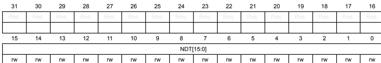
13.6.4 DMA channel x number of data to transfer register (DMA_CNDTRx)
Address offset: \( 0x0C + 0x14 * (x - 1) \) , ( \( x = 1 \) to \( 7 \) )
Reset value: 0x0000 0000
The address offsets of these registers are linked to the DMA channels availability. See Section 13.3: DMA implementation for more details.
| 31 | 30 | 29 | 28 | 27 | 26 | 25 | 24 | 23 | 22 | 21 | 20 | 19 | 18 | 17 | 16 |
| Res. | Res. | Res. | Res. | Res. | Res. | Res. | Res. | Res. | Res. | Res. | Res. | Res. | Res. | Res. | Res. |
| 15 | 14 | 13 | 12 | 11 | 10 | 9 | 8 | 7 | 6 | 5 | 4 | 3 | 2 | 1 | 0 |
| NDT[15:0] | |||||||||||||||
| rw | rw | rw | rw | rw | rw | rw | rw | rw | rw | rw | rw | rw | rw | rw | rw |
Bits 31:16 Reserved, must be kept at reset value.
Bits 15:0 NDT[15:0] : Number of data to transfer ( \( 0 \) to \( 2^{16} - 1 \) )
This bitfield is updated by hardware when the channel is enabled:
- – It is decremented after each single DMA 'read followed by write' transfer, indicating the remaining amount of data items to transfer.
- – It is kept at zero when the programmed amount of data to transfer is reached, if the channel is not in circular mode (CIRC = 0 in the DMA_CCRx register).
- – It is reloaded automatically by the previously programmed value, when the transfer is complete, if the channel is in circular mode (CIRC = 1).
If this bitfield is zero, no transfer can be served whatever the channel status (enabled or not).
Note: This bitfield is set and cleared by software. It must not be written when the channel is enabled (EN = 1). It is read-only when the channel is enabled (EN = 1).
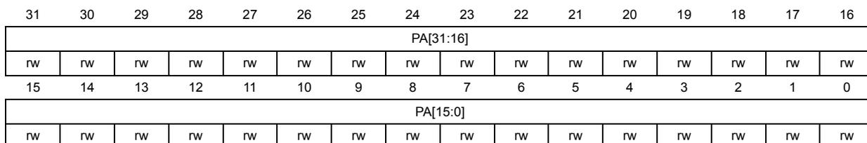
13.6.5 DMA channel x peripheral address register (DMA_CPARx)
Address offset: \( 0x10 + 0x14 * (x - 1) \) , ( \( x = 1 \) to \( 7 \) )
Reset value: 0x0000 0000
The address offsets of these registers are linked to the DMA channels availability. See Section 13.3: DMA implementation for more details.
| 31 | 30 | 29 | 28 | 27 | 26 | 25 | 24 | 23 | 22 | 21 | 20 | 19 | 18 | 17 | 16 |
| PA[31:16] | |||||||||||||||
| rw | rw | rw | rw | rw | rw | rw | rw | rw | rw | rw | rw | rw | rw | rw | rw |
| 15 | 14 | 13 | 12 | 11 | 10 | 9 | 8 | 7 | 6 | 5 | 4 | 3 | 2 | 1 | 0 |
| PA[15:0] | |||||||||||||||
| rw | rw | rw | rw | rw | rw | rw | rw | rw | rw | rw | rw | rw | rw | rw | rw |
Bits 31:0 PA[31:0] : Peripheral address
It contains the base address of the peripheral data register from/to which the data is read/written.
When PSIZE[1:0] = 01 (16 bits), bit 0 of PA[31:0] is ignored. Access is automatically aligned to a half-word address.
When PSIZE[1:0] = 10 (32 bits), bits 1 and 0 of PA[31:0] are ignored. Access is automatically aligned to a word address.
In memory-to-memory mode, this bitfield identifies the memory destination address if DIR = 1 and the memory source address if DIR = 0.
In peripheral-to-peripheral mode, this bitfield identifies the peripheral destination address if DIR = 1 and the peripheral source address if DIR = 0.
Note: This bitfield is set and cleared by software. It must not be written when the channel is enabled (EN = 1). It is not read-only when the channel is enabled (EN = 1).
13.6.6 DMA channel x memory address register (DMA_CMARx)
Address offset: 0x14 + 0x14 * (x - 1), (x = 1 to 7)
Reset value: 0x0000 0000
The address offsets of these registers are linked to the DMA channels availability. See Section 13.3: DMA implementation for more details.
| 31 | 30 | 29 | 28 | 27 | 26 | 25 | 24 | 23 | 22 | 21 | 20 | 19 | 18 | 17 | 16 |
|---|---|---|---|---|---|---|---|---|---|---|---|---|---|---|---|
| MA[31:16] | |||||||||||||||
| rw | rw | rw | rw | rw | rw | rw | rw | rw | rw | rw | rw | rw | rw | rw | rw |
| 15 | 14 | 13 | 12 | 11 | 10 | 9 | 8 | 7 | 6 | 5 | 4 | 3 | 2 | 1 | 0 |
| MA[15:0] | |||||||||||||||
| rw | rw | rw | rw | rw | rw | rw | rw | rw | rw | rw | rw | rw | rw | rw | rw |
Bits 31:0 MA[31:0] : Peripheral address
It contains the base address of the memory from/to which the data is read/written.
When MSIZE[1:0] = 01 (16 bits), bit 0 of MA[31:0] is ignored. Access is automatically aligned to a half-word address.
When MSIZE[1:0] = 10 (32 bits), bits 1 and 0 of MA[31:0] are ignored. Access is automatically aligned to a word address.
In memory-to-memory mode, this bitfield identifies the memory source address if DIR = 1 and the memory destination address if DIR = 0.
In peripheral-to-peripheral mode, this bitfield identifies the peripheral source address if DIR = 1 and the peripheral destination address if DIR = 0.
Note: This bitfield is set and cleared by software. It must not be written when the channel is enabled (EN = 1). It is not read-only when the channel is enabled (EN = 1).
13.6.7 DMA register map
Table 81. DMA register map and reset values
| Offset | Register name | 31 | 30 | 29 | 28 | 27 | 26 | 25 | 24 | 23 | 22 | 21 | 20 | 19 | 18 | 17 | 16 | 15 | 14 | 13 | 12 | 11 | 10 | 9 | 8 | 7 | 6 | 5 | 4 | 3 | 2 | 1 | 0 |
|---|---|---|---|---|---|---|---|---|---|---|---|---|---|---|---|---|---|---|---|---|---|---|---|---|---|---|---|---|---|---|---|---|---|
| 0x000 | DMA_ISR | Res. | Res. | Res. | Res. | TEIF7 | HTIF7 | TCIF7 | GIF7 | TEIF6 | HTIF6 | TCIF6 | GIF6 | TEIF5 | HTIF5 | TCIF5 | GIF5 | TEIF4 | HTIF4 | TCIF4 | GIF4 | TEIF3 | HTIF3 | TCIF3 | GIF3 | TEIF2 | HTIF2 | TCIF2 | GIF2 | TEIF1 | HTIF1 | TCIF1 | GIF1 |
| Reset value | 0 | 0 | 0 | 0 | 0 | 0 | 0 | 0 | 0 | 0 | 0 | 0 | 0 | 0 | 0 | 0 | 0 | 0 | 0 | 0 | 0 | 0 | 0 | 0 | 0 | 0 | 0 | 0 |
Table 81. DMA register map and reset values (continued)
| Offset | Register name | 31 | 30 | 29 | 28 | 27 | 26 | 25 | 24 | 23 | 22 | 21 | 20 | 19 | 18 | 17 | 16 | 15 | 14 | 13 | 12 | 11 | 10 | 9 | 8 | 7 | 6 | 5 | 4 | 3 | 2 | 1 | 0 |
|---|---|---|---|---|---|---|---|---|---|---|---|---|---|---|---|---|---|---|---|---|---|---|---|---|---|---|---|---|---|---|---|---|---|
| 0x004 | DMA_IFCR | Res. | Res. | Res. | Res. | CTEIF7 | CHIF7 | CTOIF7 | CGIF7 | CTEIF6 | CHIF6 | CTOIF6 | CGIF6 | CTEIF5 | CHIF5 | CTOIF5 | CGIF5 | CTEIF4 | CHIF4 | CTOIF4 | CGIF4 | CTEIF3 | CHIF3 | CTOIF3 | CGIF3 | CTEIF2 | CHIF2 | CTOIF2 | CGIF2 | CTEIF1 | CHIF1 | CTOIF1 | CGIF1 |
| Reset value | 0 | 0 | 0 | 0 | 0 | 0 | 0 | 0 | 0 | 0 | 0 | 0 | 0 | 0 | 0 | 0 | 0 | 0 | 0 | 0 | 0 | 0 | 0 | 0 | 0 | 0 | 0 | 0 | |||||
| 0x008 | DMA_CCR1 | Res. | Res. | Res. | Res. | Res. | Res. | Res. | Res. | Res. | Res. | Res. | Res. | Res. | Res. | Res. | Res. | MEM2MEM | PL[1:0] | MSIZE[1:0] | PSIZE[1:0] | MINC | PINC | CIRC | DIR | TEIE | HTIE | TCIE | EN | ||||
| Reset value | 0 | 0 | 0 | 0 | 0 | 0 | 0 | 0 | 0 | 0 | 0 | 0 | 0 | 0 | 0 | ||||||||||||||||||
| 0x00C | DMA_CNDTR1 | Res. | Res. | Res. | Res. | Res. | Res. | Res. | Res. | Res. | Res. | Res. | Res. | Res. | Res. | Res. | Res. | NDTR[15:0] | |||||||||||||||
| Reset value | 0 | 0 | 0 | 0 | 0 | 0 | 0 | 0 | 0 | 0 | 0 | 0 | 0 | 0 | 0 | ||||||||||||||||||
| 0x010 | DMA_CPAR1 | PA[31:0] | |||||||||||||||||||||||||||||||
| Reset value | 0 | 0 | 0 | 0 | 0 | 0 | 0 | 0 | 0 | 0 | 0 | 0 | 0 | 0 | 0 | 0 | 0 | 0 | 0 | 0 | 0 | 0 | 0 | 0 | 0 | 0 | 0 | 0 | 0 | 0 | 0 | 0 | |
| 0x014 | DMA_CMAR1 | MA[31:0] | |||||||||||||||||||||||||||||||
| Reset value | 0 | 0 | 0 | 0 | 0 | 0 | 0 | 0 | 0 | 0 | 0 | 0 | 0 | 0 | 0 | 0 | 0 | 0 | 0 | 0 | 0 | 0 | 0 | 0 | 0 | 0 | 0 | 0 | 0 | 0 | 0 | 0 | |
| 0x018 | Reserved | Reserved | |||||||||||||||||||||||||||||||
| 0x01C | DMA_CCR2 | Res. | Res. | Res. | Res. | Res. | Res. | Res. | Res. | Res. | Res. | Res. | Res. | Res. | Res. | Res. | Res. | MEM2MEM | PL[1:0] | MSIZE[1:0] | PSIZE[1:0] | MINC | PINC | CIRC | DIR | TEIE | HTIE | TCIE | EN | ||||
| Reset value | 0 | 0 | 0 | 0 | 0 | 0 | 0 | 0 | 0 | 0 | 0 | 0 | 0 | 0 | 0 | ||||||||||||||||||
| 0x020 | DMA_CNDTR2 | Res. | Res. | Res. | Res. | Res. | Res. | Res. | Res. | Res. | Res. | Res. | Res. | Res. | Res. | Res. | Res. | NDTR[15:0] | |||||||||||||||
| Reset value | 0 | 0 | 0 | 0 | 0 | 0 | 0 | 0 | 0 | 0 | 0 | 0 | 0 | 0 | 0 | ||||||||||||||||||
| 0x024 | DMA_CPAR2 | PA[31:0] | |||||||||||||||||||||||||||||||
| Reset value | 0 | 0 | 0 | 0 | 0 | 0 | 0 | 0 | 0 | 0 | 0 | 0 | 0 | 0 | 0 | 0 | 0 | 0 | 0 | 0 | 0 | 0 | 0 | 0 | 0 | 0 | 0 | 0 | 0 | 0 | 0 | 0 | |
| 0x028 | DMA_CMAR2 | MA[31:0] | |||||||||||||||||||||||||||||||
| Reset value | 0 | 0 | 0 | 0 | 0 | 0 | 0 | 0 | 0 | 0 | 0 | 0 | 0 | 0 | 0 | 0 | 0 | 0 | 0 | 0 | 0 | 0 | 0 | 0 | 0 | 0 | 0 | 0 | 0 | 0 | 0 | 0 | |
| 0x02C | Reserved | Reserved | |||||||||||||||||||||||||||||||
| 0x030 | DMA_CCR3 | Res. | Res. | Res. | Res. | Res. | Res. | Res. | Res. | Res. | Res. | Res. | Res. | Res. | Res. | Res. | Res. | MEM2MEM | PL[1:0] | MSIZE[1:0] | PSIZE[1:0] | MINC | PINC | CIRC | DIR | TEIE | HTIE | TCIE | EN | ||||
| Reset value | 0 | 0 | 0 | 0 | 0 | 0 | 0 | 0 | 0 | 0 | 0 | 0 | 0 | 0 | 0 | ||||||||||||||||||
| 0x034 | DMA_CNDTR3 | Res. | Res. | Res. | Res. | Res. | Res. | Res. | Res. | Res. | Res. | Res. | Res. | Res. | Res. | Res. | Res. | NDTR[15:0] | |||||||||||||||
| Reset value | 0 | 0 | 0 | 0 | 0 | 0 | 0 | 0 | 0 | 0 | 0 | 0 | 0 | 0 | 0 | ||||||||||||||||||
| 0x038 | DMA_CPAR3 | PA[31:0] | |||||||||||||||||||||||||||||||
| Reset value | 0 | 0 | 0 | 0 | 0 | 0 | 0 | 0 | 0 | 0 | 0 | 0 | 0 | 0 | 0 | 0 | 0 | 0 | 0 | 0 | 0 | 0 | 0 | 0 | 0 | 0 | 0 | 0 | 0 | 0 | 0 | 0 | |
| 0x03C | DMA_CMAR3 | MA[31:0] | |||||||||||||||||||||||||||||||
| Reset value | 0 | 0 | 0 | 0 | 0 | 0 | 0 | 0 | 0 | 0 | 0 | 0 | 0 | 0 | 0 | 0 | 0 | 0 | 0 | 0 | 0 | 0 | 0 | 0 | 0 | 0 | 0 | 0 | 0 | 0 | 0 | 0 | |
| 0x040 | Reserved | Reserved | |||||||||||||||||||||||||||||||
| 0x044 | DMA_CCR4 | Res. | Res. | Res. | Res. | Res. | Res. | Res. | Res. | Res. | Res. | Res. | Res. | Res. | Res. | Res. | Res. | MEM2MEM | PL[1:0] | MSIZE[1:0] | PSIZE[1:0] | MINC | PINC | CIRC | DIR | TEIE | HTIE | TCIE | EN | ||||
| Reset value | 0 | 0 | 0 | 0 | 0 | 0 | 0 | 0 | 0 | 0 | 0 | 0 | 0 | 0 | 0 | ||||||||||||||||||
| 0x048 | DMA_CNDTR4 | Res. | Res. | Res. | Res. | Res. | Res. | Res. | Res. | Res. | Res. | Res. | Res. | Res. | Res. | Res. | Res. | NDTR[15:0] | |||||||||||||||
| Reset value | 0 | 0 | 0 | 0 | 0 | 0 | 0 | 0 | 0 | 0 | 0 | 0 | 0 | 0 | 0 | ||||||||||||||||||
| 0x04C | DMA_CPAR4 | PA[31:0] | |||||||||||||||||||||||||||||||
| Reset value | 0 | 0 | 0 | 0 | 0 | 0 | 0 | 0 | 0 | 0 | 0 | 0 | 0 | 0 | 0 | 0 | 0 | 0 | 0 | 0 | 0 | 0 | 0 | 0 | 0 | 0 | 0 | 0 | 0 | 0 | 0 | 0 | |
| 0x050 | DMA_CMAR4 | MA[31:0] | |||||||||||||||||||||||||||||||
| Reset value | 0 | 0 | 0 | 0 | 0 | 0 | 0 | 0 | 0 | 0 | 0 | 0 | 0 | 0 | 0 | 0 | 0 | 0 | 0 | 0 | 0 | 0 | 0 | 0 | 0 | 0 | 0 | 0 | 0 | 0 | 0 | 0 | |
| 0x054 | Reserved | Reserved | |||||||||||||||||||||||||||||||
Table 81. DMA register map and reset values (continued)
| Offset | Register name | 31 | 30 | 29 | 28 | 27 | 26 | 25 | 24 | 23 | 22 | 21 | 20 | 19 | 18 | 17 | 16 | 15 | 14 | 13 | 12 | 11 | 10 | 9 | 8 | 7 | 6 | 5 | 4 | 3 | 2 | 1 | 0 |
|---|---|---|---|---|---|---|---|---|---|---|---|---|---|---|---|---|---|---|---|---|---|---|---|---|---|---|---|---|---|---|---|---|---|
| 0x058 | DMA_CCR5 | Res. | Res. | Res. | Res. | Res. | Res. | Res. | Res. | Res. | Res. | Res. | Res. | Res. | Res. | Res. | Res. | Res. | MEM2MEM | PL[1:0] | MSIZE[1:0] | PSIZE[1:0] | MINC | PINC | CIRC | DIR | TEIE | HTIE | TCIE | EN | |||
| Reset value | 0 | 0 | 0 | 0 | 0 | 0 | 0 | 0 | 0 | 0 | 0 | 0 | 0 | 0 | 0 | ||||||||||||||||||
| 0x05C | DMA_CNDTR5 | Res. | Res. | Res. | Res. | Res. | Res. | Res. | Res. | Res. | Res. | Res. | Res. | Res. | Res. | Res. | Res. | NDTR[15:0] | |||||||||||||||
| Reset value | 0 | 0 | 0 | 0 | 0 | 0 | 0 | 0 | 0 | 0 | 0 | 0 | 0 | 0 | 0 | 0 | |||||||||||||||||
| 0x060 | DMA_CPAR5 | PA[31:0] | |||||||||||||||||||||||||||||||
| Reset value | 0 | 0 | 0 | 0 | 0 | 0 | 0 | 0 | 0 | 0 | 0 | 0 | 0 | 0 | 0 | 0 | 0 | 0 | 0 | 0 | 0 | 0 | 0 | 0 | 0 | 0 | 0 | 0 | 0 | 0 | 0 | 0 | |
| 0x064 | DMA_CMAR5 | MA[31:0] | |||||||||||||||||||||||||||||||
| Reset value | 0 | 0 | 0 | 0 | 0 | 0 | 0 | 0 | 0 | 0 | 0 | 0 | 0 | 0 | 0 | 0 | 0 | 0 | 0 | 0 | 0 | 0 | 0 | 0 | 0 | 0 | 0 | 0 | 0 | 0 | 0 | 0 | |
| 0x068 | Reserved | Reserved | |||||||||||||||||||||||||||||||
| 0x06C | DMA_CCR6 | Res. | Res. | Res. | Res. | Res. | Res. | Res. | Res. | Res. | Res. | Res. | Res. | Res. | Res. | Res. | Res. | Res. | MEM2MEM | PL[1:0] | MSIZE[1:0] | PSIZE[1:0] | MINC | PINC | CIRC | DIR | TEIE | HTIE | TCIE | EN | |||
| Reset value | 0 | 0 | 0 | 0 | 0 | 0 | 0 | 0 | 0 | 0 | 0 | 0 | 0 | 0 | 0 | ||||||||||||||||||
| 0x070 | DMA_CNDTR6 | Res. | Res. | Res. | Res. | Res. | Res. | Res. | Res. | Res. | Res. | Res. | Res. | Res. | Res. | Res. | Res. | NDTR[15:0] | |||||||||||||||
| Reset value | 0 | 0 | 0 | 0 | 0 | 0 | 0 | 0 | 0 | 0 | 0 | 0 | 0 | 0 | 0 | 0 | |||||||||||||||||
| 0x074 | DMA_CPAR6 | PA[31:0] | |||||||||||||||||||||||||||||||
| Reset value | 0 | 0 | 0 | 0 | 0 | 0 | 0 | 0 | 0 | 0 | 0 | 0 | 0 | 0 | 0 | 0 | 0 | 0 | 0 | 0 | 0 | 0 | 0 | 0 | 0 | 0 | 0 | 0 | 0 | 0 | 0 | 0 | |
| 0x078 | DMA_CMAR6 | MA[31:0] | |||||||||||||||||||||||||||||||
| Reset value | 0 | 0 | 0 | 0 | 0 | 0 | 0 | 0 | 0 | 0 | 0 | 0 | 0 | 0 | 0 | 0 | 0 | 0 | 0 | 0 | 0 | 0 | 0 | 0 | 0 | 0 | 0 | 0 | 0 | 0 | 0 | 0 | |
| 0x07C | Reserved | Reserved | |||||||||||||||||||||||||||||||
| 0x080 | DMA_CCR7 | Res. | Res. | Res. | Res. | Res. | Res. | Res. | Res. | Res. | Res. | Res. | Res. | Res. | Res. | Res. | Res. | Res. | MEM2MEM | PL[1:0] | MSIZE[1:0] | PSIZE[1:0] | MINC | PINC | CIRC | DIR | TEIE | HTIE | TCIE | EN | |||
| Reset value | 0 | 0 | 0 | 0 | 0 | 0 | 0 | 0 | 0 | 0 | 0 | 0 | 0 | 0 | 0 | ||||||||||||||||||
| 0x084 | DMA_CNDTR7 | Res. | Res. | Res. | Res. | Res. | Res. | Res. | Res. | Res. | Res. | Res. | Res. | Res. | Res. | Res. | Res. | NDTR[15:0] | |||||||||||||||
| Reset value | 0 | 0 | 0 | 0 | 0 | 0 | 0 | 0 | 0 | 0 | 0 | 0 | 0 | 0 | 0 | 0 | |||||||||||||||||
| 0x088 | DMA_CPAR7 | PA[31:0] | |||||||||||||||||||||||||||||||
| Reset value | 0 | 0 | 0 | 0 | 0 | 0 | 0 | 0 | 0 | 0 | 0 | 0 | 0 | 0 | 0 | 0 | 0 | 0 | 0 | 0 | 0 | 0 | 0 | 0 | 0 | 0 | 0 | 0 | 0 | 0 | 0 | 0 | |
| 0x08C | DMA_CMAR7 | MA[31:0] | |||||||||||||||||||||||||||||||
| Reset value | 0 | 0 | 0 | 0 | 0 | 0 | 0 | 0 | 0 | 0 | 0 | 0 | 0 | 0 | 0 | 0 | 0 | 0 | 0 | 0 | 0 | 0 | 0 | 0 | 0 | 0 | 0 | 0 | 0 | 0 | 0 | 0 | |