9. Reset and clock control (RCC)
9.1 Reset
There are three types of reset, defined as system reset, power reset and RTC domain reset.
9.1.1 Power reset
A power reset is generated when one of the following events occurs:
- 1. Power-on/power-down reset (POR/PDR reset)
- 2. When exiting Standby mode
A power reset sets all registers to their reset values except the RTC domain (see Figure 8 ).
9.1.2 System reset
A system reset sets all registers to their reset values unless specified otherwise in the register description.
A system reset is generated when one of the following events occurs:
- 1. A low level on the NRST pin (external reset)
- 2. Window watchdog event (WWDG reset)
- 3. Independent watchdog event (IWDG reset)
- 4. A software reset (SW reset) (see Software reset )
- 5. Low-power management reset (see Low-power management reset )
- 6. Option byte loader reset (see Option byte loader reset )
- 7. A power reset
The reset source can be identified by checking the reset flags in the Control/Status register, RCC_CSR (see Section 9.4.10: Control/status register (RCC_CSR) ).
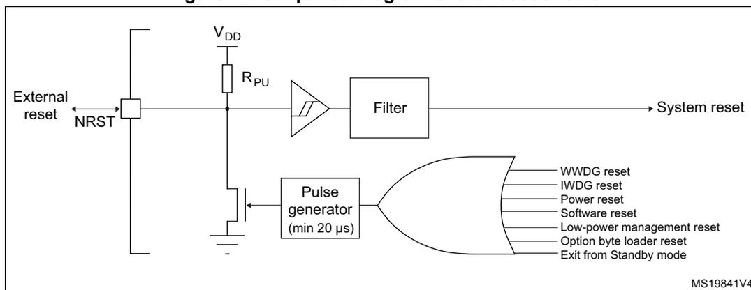
These sources act on the NRST pin and it is always kept low during the delay phase. The RESET service routine vector is fixed at address 0x0000_0004 in the memory map.
The system reset signal provided to the device is output on the NRST pin. The pulse generator guarantees a minimum reset pulse duration of 20 µs for each internal reset source. In case of an external reset, the reset pulse is generated while the NRST pin is asserted low.
Figure 12. Simplified diagram of the reset circuit
Software reset
The SYSRESETREQ bit in Cortex-M4 ® F application interrupt and reset control register must be set to force a software reset on the device. Refer to the STM32 Cortex ® -M4 MCUs and MPUs programming manual (PM0214) for more details.
Low-power management reset
There are two ways to generate a low-power management reset:
- 1. Reset generated when entering Standby mode:
This type of reset is enabled by resetting nRST_STDBY bit in User Option Bytes. In this case, whenever a Standby mode entry sequence is successfully executed, the device is reset instead of entering Standby mode. - 2. Reset when entering Stop mode:
This type of reset is enabled by resetting nRST_STOP bit in User Option Bytes. In this case, whenever a Stop mode entry sequence is successfully executed, the device is reset instead of entering Stop mode.
For further information on the User Option Bytes, refer to Section 5: Option byte description .
Option byte loader reset
The option byte loader reset is generated when the OBL_LAUNCH bit (bit 13) is set in the FLASH_CR register. This bit is used to launch the option byte loading by software.
9.1.3 RTC domain reset
The RTC domain has two specific resets that affect only the RTC domain ( Figure 8 ).
An RTC domain reset only affects the LSE oscillator, the RTC, the Backup registers, and the RCC RTC domain control register (RCC_BDCR) . It is generated when one of the following events occurs.
- 1. Software reset, triggered by setting the BDRST bit in the RTC domain control register (RCC_BDCR) .
- 2. V DD power-up if V BAT has been disconnected when it was low.
The backup registers are also reset when one of the following events occurs:
- 1. RTC tamper detection event.
- 2. Change of the read out protection from level 1 to level 0.
9.2 Clocks
Three different clock sources can be used to drive the system clock (SYSCLK):
- • HSI 8 MHz RC oscillator clock
- • HSE oscillator clock
- • PLL clock
The devices have the following additional clock sources:
- • 40 kHz low speed internal RC (LSI RC) which drives the independent watchdog and optionally the RTC used for Auto-wakeup from Stop/Standby mode.
- • 32.768 kHz low speed external crystal (LSE crystal) which optionally drives the real-time clock (RTCCLK)
Each clock source can be switched on or off independently when it is not used, to optimize power consumption.
Several prescalers can be used to configure the AHB frequency, the high speed APB (APB2) and the low speed APB (APB1) domains. The maximum frequency of the AHB and APB2 domains is 72 MHz. The maximum allowed frequency of the APB1 domain is 36 MHz.
All the peripheral clocks are derived from their bus clock (HCLK, PCLK1 or PCLK2) except:
- • The flash memory programming interface clock (FLITFCLK) which is always the HSI clock.
- • The 48-MHz USB clock which is derived from the PLL VCO (STM32F303xB/C/D/E devices)
- • The option byte loader clock, which is always the HSI clock
- • The ADCs clock, which is derived from the PLL output. It can reach 72 MHz and can then be divided by 1,2,4,6,8,10,12,16,32,64,128 or 256.
- • The U(S)ARTs clock, which is derived (selected by software) from one of the four following sources:
- – system clock
- – HSI clock
- – LSE clock
- – APB1 or APB2 clock (PCLK1 or PCLK2 depending on which APB is mapped the USART)
- • The I2C1/2 (I2C1/2/3 in STM32F303xD/E and STM32F398xE) clock, which is derived (selected by software) from one of the two following sources:
- – system clock
- – HSI clock
- • The I2S2 and I2S3 clocks, which can be derived from an external dedicated clock source.
- • The RTC clock which is derived from the LSE, LSI or from the HSE clock divided by 32.
- • The IWDG clock, which is always the LSI clock.
The RCC feeds the Cortex System Timer (SysTick) external clock with the AHB clock (HCLK) divided by 8. The SysTick can work either with this clock or directly with the Cortex clock (HCLK), configurable in the SysTick Control and Status Register.
Figure 13. STM32F303xB/C and STM32F358xC clock tree
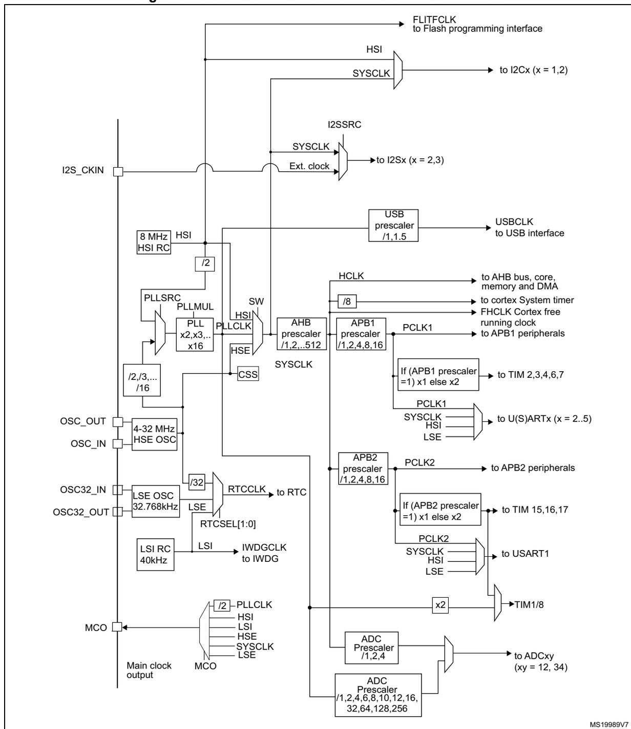
The diagram illustrates the internal clock architecture. On the left, external and internal clock sources are shown:
- I2S_CKIN : Input for I2S clock.
- OSC_OUT and OSC_IN : Connected to a 4-32 MHz HSE OSC.
- OSC32_IN and OSC32_OUT : Connected to a 32.768kHz LSE OSC.
- LSI RC : 40kHz internal low-speed oscillator.
- HSI : 8 MHz internal high-speed oscillator.
- MCO : Main clock output pin, selectable from HSI, LSI, HSE, SYSCLK, or PLLCLK (divided by 2).
- APB1 prescaler (/1, 2, 4, 8, 16) generates PCLK1 for APB1 peripherals and TIM 2,3,4,6,7. A multiplexer can also select SYSCLK, HSI, or LSE for U(S)ARTx (x = 2..5).
- APB2 prescaler (/1, 2, 4, 8, 16) generates PCLK2 for APB2 peripherals and TIM 15,16,17. A multiplexer can also select SYSCLK, HSI, or LSE for USART1.
- FLITFCLK : to Flash programming interface.
- HSI and SYSCLK : to I2Cx (x = 1,2).
- SYSCLK (from I2SSRC) and Ext. clock : to I2Sx (x = 2,3).
- USBCLK (from USB prescaler /1, 1.5): to USB interface.
- RTCCLK (from LSE or HSE divided by 32): to RTC.
- IWDGCLK (from LSI): to IWDG.
- ADCCLK (from HCLK prescalers /1, 2, 4 or /1, 2, 4, 6, 8, 10, 12, 16, 32, 64, 128, 256): to ADCx y (xy = 12, 34).
- TIM1/8 : clocked from PLLCLKx2.
MS19989V7
- 1. For full details about the internal and external clock source characteristics, refer to the “Electrical characteristics” section in your device datasheet.
- 2. TIM1 and TIM8 can be clocked from the PLLCLKx2 running up to 144 MHz when the system clock source is the PLL and
the AHB and APB2 prescalers are set to '1'.
- 3. The ADC clock can be derived from the AHB clock of the ADC bus interface, divided by a programmable factor (1, 2 or 4). When the programmable factor is '1', the AHB prescaler must be equal to '1'.
Figure 14. STM32F303xDxE and STM32F398xE clock tree
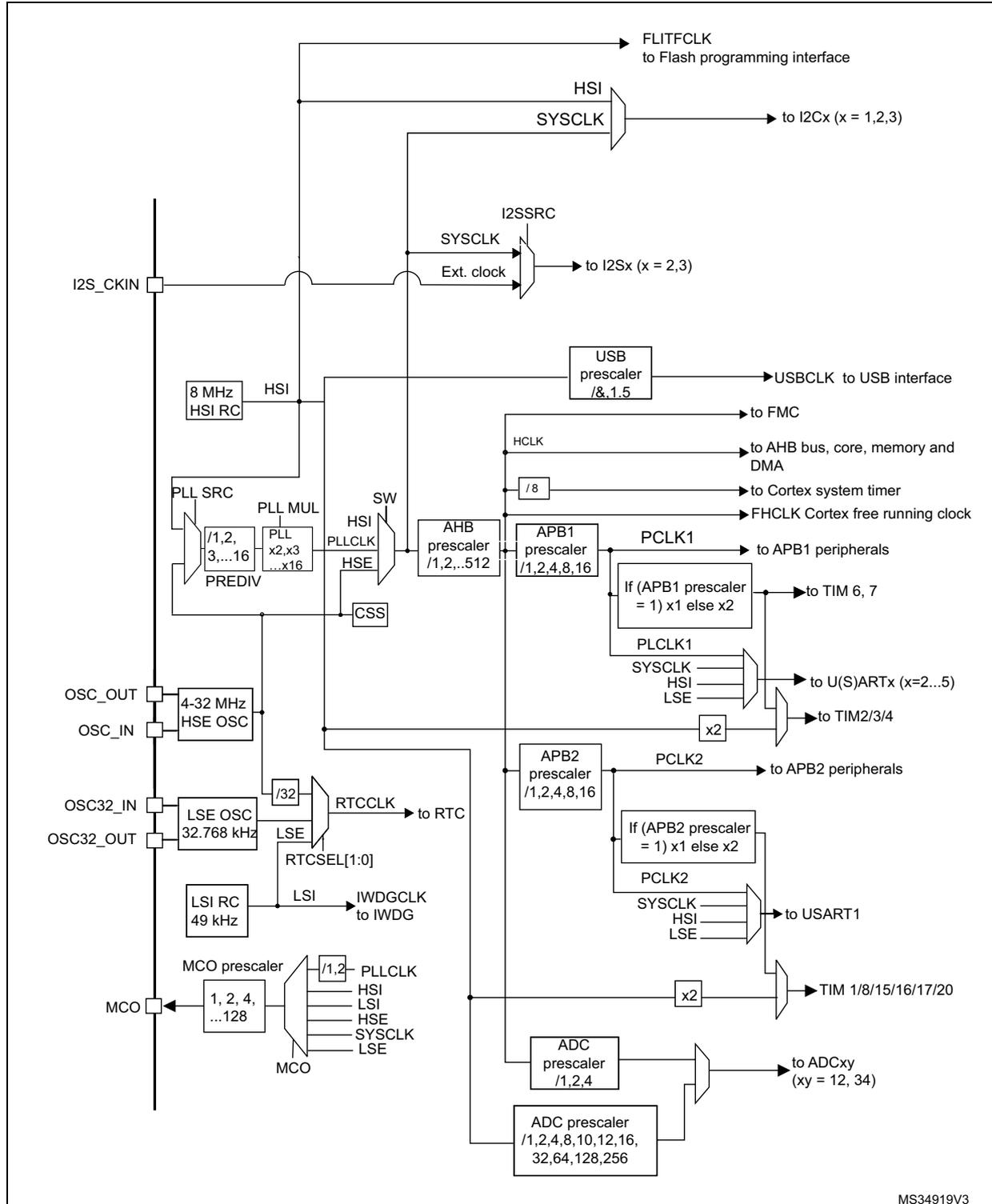
The diagram illustrates the clock tree architecture for STM32F303xDxE and STM32F398xE. It starts with several clock sources on the left:
- HSI (8 MHz) and HSI RC provide internal clock signals.
- HSE OSC (4-32 MHz) is connected via OSC_IN and OSC_OUT pins.
- LSE OSC (32.768 kHz) is connected via OSC32_IN and OSC32_OUT pins.
- LSI RC (49 kHz) provides a low-speed internal clock.
- PLL is configured via PLL_SRC , PREDIV (/1,2,3,...16), and PLL_MUL (x2,x3,...x16).
- An external clock can be provided via the I2S_CKIN pin.
- FLITFCLK to the Flash programming interface.
- HSI to I2Cx (x = 1,2,3).
- SYSCLOCK is derived from the main clock and used for I2SSRC and Ext. clock to I2Sx (x = 2,3).
- HCLK is derived from the main clock and divided by AHB prescaler (/1,2,...512). It is further divided by /8 to provide FHCLK to the Cortex system timer and to the USB prescaler (/&1.5) for USBCLK to the USB interface.
- HCLK also feeds into APB1 prescaler (/1,2,4,8,16) to generate PCLK1 for APB1 peripherals. PCLK1 is further divided (If (APB1 prescaler = 1) x1 else x2) for TIM 6, 7 and multiplied by x2 for U(S)ARTx (x=2...5) and TIM2/3/4 .
- HCLK also feeds into APB2 prescaler (/1,2,4,8,16) to generate PCLK2 for APB2 peripherals. PCLK2 is further divided (If (APB2 prescaler = 1) x1 else x2) for USART1 and multiplied by x2 for TIM 1/8/15/16/17/20 .
- HCLK also feeds into ADC prescaler (/1,2,4) for ADCx (xy = 12, 34). Another ADC prescaler (/1,2,4,8,10,12,16,32,64,128,256) is also shown.
- LSI (49 kHz) is used for IWDGCLK to the IWDG.
- LSE (32.768 kHz) is used for RTCCLK to the RTC, selected via RTCSEL[1:0] .
- The MCO pin outputs a selectable clock signal ( PLLCLK , HSI , LSI , HSE , SYSCLOCK , or LSE ) divided by the MCO prescaler (1, 2, 4, ..., 128).
MS34919V3
- 1. For full details about the internal and external clock source characteristics, please refer to the Electrical characteristics section in the device datasheet.
- 2. TIMx (x = 1/2/3/4/8/15/16/17/20) can be clocked from the PLL running at 144 MHz when the system clock source is the PLL and AHB or APB2 subsystem clocks are not divided by more than 2 cumulatively.
- 3. The ADC clock can be derived from the AHB clock of the ADC bus interface, divided by a programmable factor (1, 2 or 4). When the programmable factor is "1", the AHB prescaler must be equal to "1".
Figure 15. STM32F303x6/8 and STM32F328x8 clock tree
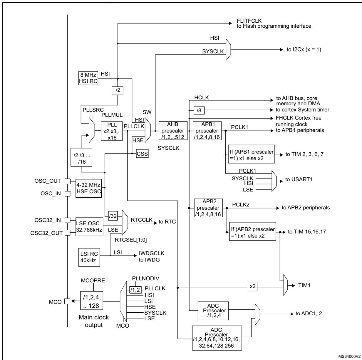
The diagram illustrates the clock tree architecture. At the top, the FLITFCLK is derived from the HSI. The HSI (8 MHz) is also divided by 2 to provide the SYSCLK to the I2Cx (x = 1). The PLL is configured with PLLSRC (HSI or HSE) and PLLMUL (x2, x3, ..., x16). The PLL output (PLLCLK) is divided by 8 to provide the HCLK to the AHB bus, core, memory, and DMA, and to the cortex System timer. The HCLK is also divided by 8 to provide the FHCLK (Cortex free running clock) to APB1 peripherals. The SYSCLK is derived from the PLLCLK via a switch (SW) and is divided by 1/2, 1/3, ..., 1/16 to provide the PCLK1 to APB1 peripherals. The PCLK1 is also divided by 1/2, 1/4, 1/8, 1/16 to provide the PCLK2 to APB2 peripherals. The PCLK1 is also divided by 1/2, 1/4, 1/8, 1/16 to provide the PCLK1 to TIM 2, 3, 6, 7. The PCLK1 is also divided by 1/2, 1/4, 1/8, 1/16 to provide the PCLK1 to USART1. The PCLK2 is also divided by 1/2, 1/4, 1/8, 1/16 to provide the PCLK2 to TIM 15, 16, 17. The PCLK2 is also divided by 1/2, 1/4, 1/8, 1/16 to provide the PCLK2 to ADC1, 2. The ADC clock is derived from the AHB clock of the ADC bus interface, divided by a programmable factor (1, 2 or 4). When the programmable factor is "1", the AHB prescaler must be equal to "1". The MCO output is derived from the HSI, PLLCLK, LSI, HSE, SYSCLK, or LSE via a prescaler (1/2, 4, ..., 128). The RTCCLK is derived from the LSE (32.768kHz) via a prescaler (1/32). The IWDGCLK is derived from the LSI (40kHz).
MS34000V2
- 1. For full details about the internal and external clock source characteristics, refer to the "Electrical characteristics" section in your device datasheet.
- 2. TIM1 can be clocked from the PLL running at 144 MHz when the system clock source is the PLL and AHB or APB2 subsystem clocks are not divided by more than 2 cumulatively.
- 3. The ADC clock can be derived from the AHB clock of the ADC bus interface, divided by a programmable factor (1, 2 or 4). When the programmable factor is '1', the AHB prescaler must be equal to '1'.
FCLK acts as Cortex-M4 ® F free-running clock. For more details, refer to the STM32 Cortex ® -M4 MCUs and MPUs programming manual (PM0214).
9.2.1 HSE clock
The high speed external clock signal (HSE) can be generated from two possible clock sources:
- • HSE external crystal/ceramic resonator
- • HSE user external clock
The resonator and the load capacitors have to be placed as close as possible to the oscillator pins to minimize output distortion and startup stabilization time. The loading capacitance values must be adjusted according to the selected oscillator.
Figure 16. HSE/ LSE clock sources
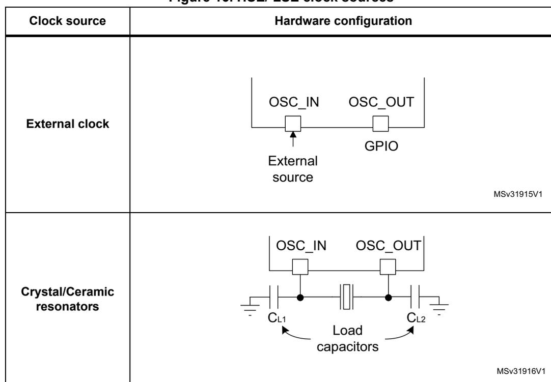
| Clock source | Hardware configuration |
|---|---|
| External clock | MSV31915V1 |
| Crystal/Ceramic resonators | MSV31916V1 |
External crystal/ceramic resonator (HSE crystal)
The 4 to 32 MHz external oscillator has the advantage of producing a very accurate rate on the main clock.
The associated hardware configuration is shown in Figure 16 . Refer to the electrical characteristics section of the datasheet for more details.
The HSERDY flag in the Clock control register (RCC_CR) indicates if the HSE oscillator is stable or not. At startup, the clock is not released until this bit is set by hardware. An interrupt can be generated if enabled in the Clock interrupt register (RCC_CIR) .
The HSE Crystal can be switched on and off using the HSEON bit in the Clock control register (RCC_CR) .
Caution: To switch ON the HSE oscillator, 512 HSE clock pulses need to be seen by an internal stabilization counter after the HSEON bit is set. Even in the case that no crystal or resonator is connected to the device, excessive external noise on the OSC_IN pin may still lead the oscillator to start. Once the oscillator is started, it needs another 6 HSE clock pulses to complete a switching OFF sequence. If for any reason the oscillations are no more present on the OSC_IN pin, the oscillator cannot be switched OFF, locking the OSC pins from any other use and introducing unwanted power consumption. To avoid such situation, it is strongly recommended to always enable the Clock Security System (CSS) which is able to switch OFF the oscillator even in this case.
External source (HSE bypass)
In this mode, an external clock source must be provided. It can have a frequency of up to 32 MHz. Select this mode by setting the HSEBYP and HSEON bits in the Clock control register (RCC_CR) . The external clock signal (square, sinus or triangle) with ~40-60% duty cycle depending on the frequency (refer to the datasheet ) has to drive the OSC_IN pin while the OSC_OUT pin can be used a GPIO. See Figure 16 .
9.2.2 HSI clock
The HSI clock signal is generated from an internal 8 MHz RC Oscillator and can be used directly as a system clock or divided by 2 to be used as PLL input.
The HSI RC oscillator has the advantage of providing a clock source at low cost (no external components). It also has a faster startup time than the HSE crystal oscillator however, even with calibration the frequency is less accurate than an external crystal oscillator or ceramic resonator.
Calibration
RC oscillator frequencies can vary from one chip to another due to manufacturing process variations, this is why each device is factory calibrated by ST for 1% accuracy at \( T_A=25^\circ\text{C} \) .
After reset, the factory calibration value is loaded in the HSICAL[7:0] bits in the Clock control register (RCC_CR) .
If the application is subject to voltage or temperature variations this may affect the RC oscillator speed. The user can trim the HSI frequency in the application using the HSITRIM[4:0] bits in the Clock control register (RCC_CR) .
For more details on how to measure the HSI frequency variation, refer to Section 9.2.14: Internal/external clock measurement with TIM16 .
The HSIRDY flag in the Clock control register (RCC_CR) indicates if the HSI RC is stable or not. At startup, the HSI RC output clock is not released until this bit is set by hardware.
The HSI RC can be switched on and off using the HSION bit in the Clock control register (RCC_CR) .
The HSI signal can also be used as a backup source (Auxiliary clock) if the HSE crystal oscillator fails. Refer to Section 9.2.7: Clock security system (CSS) on page 134 .
9.2.3 PLL
The internal PLL can be used to multiply the HSI or HSE output clock frequency. Refer to Figure 13 and Clock control register (RCC_CR) .
The PLL configuration (selection of the input clock, and multiplication factor) must be done before enabling the PLL. Once the PLL is enabled, these parameters cannot be changed.
To modify the PLL configuration, proceed as follows:
- 1. Disable the PLL by setting PLLON to 0.
- 2. Wait until PLLRDY is cleared. The PLL is now fully stopped.
- 3. Change the desired parameter.
- 4. Enable the PLL again by setting PLLON to 1.
An interrupt can be generated when the PLL is ready, if enabled in the Clock interrupt register (RCC_CIR) .
The PLL output frequency must be set in the range 16-72 MHz.
9.2.4 LSE clock
The LSE crystal is a 32.768 kHz Low Speed External crystal or ceramic resonator. It has the advantage of providing a low-power but highly accurate clock source to the real-time clock peripheral (RTC) for clock/calendar or other timing functions.
The LSE crystal is switched on and off using the LSEON bit in RTC domain control register (RCC_BDCR) . The crystal oscillator driving strength can be changed at runtime using the LSEDRV[1:0] bits in the RTC domain control register (RCC_BDCR) to obtain the best compromise between robustness and short start-up time on one side and low-power-consumption on the other.
The LSERDY flag in the RTC domain control register (RCC_BDCR) indicates whether the LSE crystal is stable or not. At startup, the LSE crystal output clock signal is not released until this bit is set by hardware. An interrupt can be generated if enabled in the Clock interrupt register (RCC_CIR) .
Caution: To switch ON the LSE oscillator, 4096 LSE clock pulses need to be seen by an internal stabilization counter after the LSEON bit is set. Even in the case that no crystal or resonator is connected to the device, excessive external noise on the OSC32_IN pin may still lead the oscillator to start. Once the oscillator is started, it needs another 6 LSE clock pulses to complete a switching OFF sequence. If for any reason the oscillations are no more present on the OSC_IN pin, the oscillator cannot be switched OFF, locking the OSC32 pins from any other use and introducing unwanted power consumption. The only way to recover such situation is to perform the RTC domain reset by software.
External source (LSE bypass)
In this mode, an external clock source must be provided. It can have a frequency of up to 1 MHz. Select this mode by setting the LSEBYP and LSEON bits in the RTC domain control register (RCC_BDCR) . The external clock signal (square, sinus, or triangle) with ~50% duty cycle has to drive the OSC32_IN pin while the OSC32_OUT pin can be used as GPIO. See Figure 16 .
9.2.5 LSI clock
The LSI RC acts as a low-power clock source that can be kept running in Stop and Standby mode for the independent watchdog (IWDG) and RTC. The clock frequency is around 40 kHz (between 30 kHz and 50 kHz). For more details, refer to the electrical characteristics section of the datasheets.
The LSI RC can be switched on and off using the LSION bit in the Control/status register (RCC_CSR) .
The LSIRDY flag in the Control/status register (RCC_CSR) indicates if the LSI oscillator is stable or not. At startup, the clock is not released until this bit is set by hardware. An interrupt can be generated if enabled in the Clock interrupt register (RCC_CIR) .
9.2.6 System clock (SYSCLK) selection
Three different clock sources can be used to drive the system clock (SYSCLK):
- • HSI oscillator
- • HSE oscillator
- • PLL
After a system reset, the HSI oscillator is selected as system clock. When a clock source is used directly or through the PLL as a system clock, it is not possible to stop it.
A switch from one clock source to another occurs only if the target clock source is ready (clock stable after startup delay or PLL locked). If a clock source, which is not yet ready is selected, the switch occurs when the clock source becomes ready. Status bits in the Clock control register (RCC_CR) indicate which clock(s) is (are) ready and which clock is currently used as a system clock.
9.2.7 Clock security system (CSS)
Clock Security System can be activated by software. In this case, the clock detector is enabled after the HSE oscillator startup delay, and disabled when this oscillator is stopped.
If a failure is detected on the HSE clock, the HSE oscillator is automatically disabled, a clock failure event is sent to the break input of the advanced-control timers (TIM1/TIM8 and TIM15/16/17) and an interrupt is generated to inform the software about the failure (Clock Security System Interrupt CSSI), allowing the MCU to perform rescue operations. The CSSI is linked to the Cortex-M4 ® F NMI (non-maskable interrupt) exception vector.
Note: Once the CSS is enabled and if the HSE clock fails, the CSS interrupt occurs and an NMI is automatically generated. The NMI is executed indefinitely unless the CSS interrupt pending bit is cleared. As a consequence, in the NMI ISR user must clear the CSS interrupt by setting the CSSC bit in the Clock interrupt register (RCC_CIR) .
If the HSE oscillator is used directly or indirectly as the system clock (indirectly means: it is used as PLL input clock, and the PLL clock is used as system clock), a detected failure
causes a switch of the system clock to the HSI oscillator and the disabling of the HSE oscillator. If the HSE clock (divided or not) is the clock entry of the PLL used as system clock when the failure occurs, the PLL is disabled too.
9.2.8 ADC clock
The ADC clock is derived from the PLL output. It can reach 72 MHz and can be divided by the following prescalers values: 1, 2, 4, 6, 8, 10, 12, 16, 32, 64, 128 or 256. It is asynchronous to the AHB clock. Alternatively, the ADC clock can be derived from the AHB clock of the ADC bus interface, divided by a programmable factor (1, 2 or 4). This programmable factor is configured using the CKMODE bit fields in the ADCx_CCR.
If the programmed factor is '1', the AHB prescaler must be set to '1'.
9.2.9 RTC clock
The RTCCLK clock source can be either the HSE/32, LSE or LSI clock. It is selected by programming the RTCSEL[1:0] bits in the RTC domain control register (RCC_BDCR) . This selection cannot be modified without resetting the RTC domain. The system must always be configured so as to get a PCLK frequency greater than or equal to the RTCCLK frequency for a proper operation of the RTC.
The LSE clock is in the RTC domain, whereas the HSE and LSI clocks are not. Consequently:
- • If LSE is selected as RTC clock:
- – The RTC continues to work even if the \( V_{DD} \) supply is switched off, provided the \( V_{BAT} \) supply is maintained.
- – The RTC remains clocked and functional under system reset.
- • If LSI is selected as the RTC clock:
- – The RTC state is not guaranteed if the \( V_{DD} \) supply is powered off.
- • If the HSE clock divided by 32 is used as the RTC clock:
- – The RTC state is not guaranteed if the \( V_{DD} \) supply is powered off or if the internal voltage regulator is powered off (removing power from the 1.8 V domain).
9.2.10 Timers (TIMx) clock
APB clock source
The timers clock frequencies are automatically defined by hardware. There are two cases:
- 1. If the APB prescaler equals 1, the timer clock frequencies are set to the same frequency as that of the APB domain.
- 2. Otherwise, they are set to twice ( \( \times 2 \) ) the frequency of the APB domain.
PLL clock source
A clock issued from the PLL (PLLCLK \( \times 2 \) ) can be selected for TIMx ( \( x = 1, 8 \) on the STM32F303xB/C and STM32F358xC; \( x = 1, 2, 3, 4, 8, 15, 16, 17, 20 \) on STM32F303xD/E; \( x = 1 \) on the STM32F303x6/8 and STM32F328x8). This configuration allows to feed TIMx with a frequency up to 144 MHz when the system clock source is the PLL.
In this configuration:
- • On the STM32F303xB/C and STM32F358xC, AHB and APB2 prescalers are set to 1, that is, AHB and APB2 clocks are not divided with respect to the system clock.
- • On the STM32F303xD/E, STM32F303x6/8 and STM32F328x8 AHB or APB2 subsystem clocks are not divided by more than 2 cumulatively with respect to the system clock.
9.2.11 Watchdog clock
If the Independent watchdog (IWDG) is started by either hardware option or software access, the LSI oscillator is forced ON and cannot be disabled. After the LSI oscillator temporization, the clock is provided to the IWDG.
9.2.12 I2S clock (only in STM32F303xB/C/D/E, STM32F358xC and STM32F398xE)
The I2S clock can be either the System clock or an external clock provided on I2S_CKIN pin. The selection of the I2S clock source is performed using bit 23 (I2SSRC) of RCC_CFGR register.
9.2.13 Clock-out capability
The microcontroller clock output (MCO) capability allows the clock to be output onto the external MCO pin. The configuration registers of the corresponding GPIO port must be programmed in alternate function mode. One of 5 clock signals can be selected as the MCO clock.
- • LSI
- • LSE
- • SYSCLK
- • HSI
- • HSE
- • PLL clock divided by 2
The selection is controlled by the MCO[2:0] bits in the Clock configuration register (RCC_CFGR) .
On the STM32F303xD/E, STM32F303x6/8 and STM32F328x8, the additional bit PLLNODIV in this register controls the divider bypass for a PLL clock input to MCO. The MCO frequency can be reduced by a configurable divider, controlled by the MCOPRE[2:0] bits of the Clock configuration register (RCC_CFGR).
9.2.14 Internal/external clock measurement with TIM16
It is possible to indirectly measure the frequency of all on-board clock sources by means of the TIM16 channel 1 input capture. As represented on Figure 17 .
Figure 17. Frequency measurement with TIM16 in capture mode
![Diagram showing the connection of various clock sources to the TIM16 TI1 input capture channel via a multiplexer controlled by TI1_RMP[1:0] bits.](/RM0316-STM32F303xB-C-D-E-303x6-8-328x8-358xC-398xE/6ebc3724d8a9c6dac981f189ea2e77dc_img.jpg)
The diagram illustrates a multiplexer (MUX) with four input options: GPIO, RTCCLK, HSE/32, and MCO. The output of the MUX is connected to the TI1 input of a TIM16 timer block. Above the MUX, the control signal is labeled TI1_RMP[1:0]. The TIM16 block is shown as a rectangle with the label 'TIM16' inside. In the bottom right corner of the diagram area, the identifier 'MS30477V1' is present.
The input capture channel of the Timer 16 can be a GPIO line or an internal clock of the MCU. This selection is performed through the TI1_RMP [1:0] bits in the TIM16_OR register. The possibilities available are the following ones.
- • TIM16 Channel1 is connected to the GPIO. Refer to the alternate function mapping in the device datasheets.
- • TIM16 Channel1 is connected to the RTCCLK.
- • TIM16 Channel1 is connected to the HSE/32 Clock.
- • TIM16 Channel1 is connected to the microcontroller clock output (MCO), this selection is controlled by the MCO[2:0] bits of the Clock configuration register (RCC_CFGR).
Calibration of the HSI
The primary purpose of connecting the LSE, through the MCO multiplexer, to the channel 1 input capture is to be able to precisely measure the HSI system clocks (for this, the HSI should be used as the system clock source). The number of HSI clock counts between consecutive edges of the LSE signal provides a measure of the internal clock period. Taking advantage of the high precision of LSE crystals (typically a few tens of ppm's), it is possible to determine the internal clock frequency with the same resolution, and trim the source to compensate for manufacturing-process- and/or temperature- and voltage-related frequency deviations.
The HSI oscillator has dedicated user-accessible calibration bits for this purpose.
The basic concept consists in providing a relative measurement (for example, the HSI/LSE ratio): the precision is therefore closely related to the ratio between the two clock sources. The higher the ratio is, the better the measurement is.
If LSE is not available, HSE/32 is the better option to reach the most precise calibration possible.
Calibration of the LSI
The calibration of the LSI follows the same pattern that for the HSI, but changing the reference clock. It is necessary to connect LSI clock to the channel 1 input capture of the TIM16. Then define the HSE as system clock source, the number of his clock counts between consecutive edges of the LSI signal provides a measure of the internal low speed clock period.
The basic concept consists in providing a relative measurement (for example, the HSE/LSI ratio): the precision is therefore closely related to the ratio between the two clock sources. The higher the ratio is, the better the measurement is.
9.3 Low-power modes
APB peripheral clocks and DMA clock can be disabled by software.
Sleep mode stops the CPU clock. The memory interface clocks (Flash and RAM interfaces) can be stopped by software during sleep mode. The AHB to APB bridge clocks are disabled by hardware during Sleep mode when all the clocks of the peripherals connected to them are disabled.
Stop mode stops all the clocks in the V18 domain and disables the PLL, the HSI and the HSE oscillators.
All U(S)ARTs and I2Cs have the capability to enable the HSI oscillator even when the MCU is in Stop mode (if HSI is selected as the clock source for that peripheral).
All U(S)ARTs can also be driven by the LSE oscillator when the system is in Stop mode (if LSE is selected as clock source for that peripheral) and the LSE oscillator is enabled (LSEON) but they do not have the capability to turn on the LSE oscillator.
Standby mode stops all the clocks in the V18 domain and disables the PLL and the HSI and HSE oscillators.
The CPU's deepsleep mode can be overridden for debugging by setting the DBG_STOP or DBG_STANDBY bits in the DBGMCU_CR register.
When waking up from deepsleep after an interrupt (Stop mode) or reset (Standby mode), the HSI oscillator is selected as system clock.
If a flash programming operation is on going, deep-sleep mode entry is delayed until the flash interface access is finished. If an access to the APB domain is ongoing, deepsleep mode entry is delayed until the APB access is finished.
9.4 RCC registers
Refer to Section 2.2 for a list of abbreviations used in register descriptions.
9.4.1 Clock control register (RCC_CR)
Address offset: 0x00
Reset value: 0x0000 XX83
(where X is undefined)
Access: no wait state, word, half-word, and byte access
| 31 | 30 | 29 | 28 | 27 | 26 | 25 | 24 | 23 | 22 | 21 | 20 | 19 | 18 | 17 | 16 |
|---|---|---|---|---|---|---|---|---|---|---|---|---|---|---|---|
| Res. | Res. | Res. | Res. | Res. | Res. | PLL RDY | PLLON | Res. | Res. | Res. | Res. | CSS ON | HSE BYP | HSE RDY | HSE ON |
| r | rw | rw | rw | r | rw | ||||||||||
| 15 | 14 | 13 | 12 | 11 | 10 | 9 | 8 | 7 | 6 | 5 | 4 | 3 | 2 | 1 | 0 |
| HSICAL[7:0] | HSITRIM[4:0] | Res. | HSI RDY | HSION | |||||||||||
| r | r | r | r | r | r | r | r | rw | rw | rw | rw | rw | r | rw | |
Bits 31:26 Reserved, must be kept at reset value.
Bit 25 PLL RDY : PLL clock ready flag
Set by hardware to indicate that the PLL is locked.
0: PLL unlocked
1: PLL locked
Bit 24 PLLON : PLL enable
Set and cleared by software to enable PLL.
Cleared by hardware when entering Stop or Standby mode. This bit can not be reset if the PLL clock is used as system clock or is selected to become the system clock.
0: PLL OFF
1: PLL ON
Bits 23:20 Reserved, must be kept at reset value.
Bit 19 CSSON : Clock security system enable
Set and cleared by software to enable the clock security system. When CSSON is set, the clock detector is enabled by hardware when the HSE oscillator is ready, and disabled by hardware if a HSE clock failure is detected.
0: Clock detector OFF
1: Clock detector ON (Clock detector ON if the HSE oscillator is ready, OFF if not).
Bit 18 HSEBYP : HSE crystal oscillator bypass
Set and cleared by software to bypass the oscillator with an external clock. The external clock must be enabled with the HSEON bit set, to be used by the device. The HSEBYP bit can be written only if the HSE oscillator is disabled.
0: HSE crystal oscillator not bypassed
1: HSE crystal oscillator bypassed with external clock
Bit 17 HSERDY: HSE clock ready flag
Set by hardware to indicate that the HSE oscillator is stable. This bit needs 6 cycles of the HSE oscillator clock to fall down after HSEON reset.
0: HSE oscillator not ready
1: HSE oscillator ready
Bit 16 HSEON: HSE clock enable
Set and cleared by software.
Cleared by hardware to stop the HSE oscillator when entering Stop or Standby mode. This bit cannot be reset if the HSE oscillator is used directly or indirectly as the system clock.
0: HSE oscillator OFF
1: HSE oscillator ON
Bits 15:8 HSICAL[7:0]: HSI clock calibration
These bits are initialized automatically at startup.
Bits 7:3 HSITRIM[4:0]: HSI clock trimming
These bits provide an additional user-programmable trimming value that is added to the HSICAL[7:0] bits. It can be programmed to adjust to variations in voltage and temperature that influence the frequency of the HSI.
The default value is 16, which, when added to the HSICAL value, should trim the HSI to 8 MHz \( \pm \) 1%. The trimming step ( \( F_{\text{hsitrim}} \) ) is around 40 kHz between two consecutive HSICAL steps.
Bit 2 Reserved, must be kept at reset value.
Bit 1 HSIRDY: HSI clock ready flag
Set by hardware to indicate that HSI oscillator is stable. After the HSION bit is cleared, HSIRDY goes low after 6 HSI oscillator clock cycles.
0: HSI oscillator not ready
1: HSI oscillator ready
Bit 0 HSION: HSI clock enable
Set and cleared by software.
Set by hardware to force the HSI oscillator ON when leaving Stop or Standby mode or in case of failure of the HSE crystal oscillator used directly or indirectly as system clock. This bit cannot be reset if the HSI is used directly or indirectly as system clock or is selected to become the system clock.
0: HSI oscillator OFF
1: HSI oscillator ON
9.4.2 Clock configuration register (RCC_CFGR)
Address offset: 0x04
Reset value: 0x0000 0000
Access: 0 ≤ wait state ≤ 2, word, half-word and byte access
1 or 2 wait states inserted only if the access occurs during clock source switch.
| 31 | 30 | 29 | 28 | 27 | 26 | 25 | 24 | 23 | 22 | 21 | 20 | 19 | 18 | 17 | 16 |
|---|---|---|---|---|---|---|---|---|---|---|---|---|---|---|---|
| PLLNO DIV | MCOPRE[2:1] | MCOF/ MCOP RE0 | Res | MCO[2:0] | I2SSRC | USBPR E | PLLMUL[3:0] | PLL XTPRE | PLL SRC | ||||||
| rw | rw | rw | r / rw | rw | rw | rw | rw | rw | rw | rw | rw | rw | rw | rw | |
| 15 | 14 | 13 | 12 | 11 | 10 | 9 | 8 | 7 | 6 | 5 | 4 | 3 | 2 | 1 | 0 |
|---|---|---|---|---|---|---|---|---|---|---|---|---|---|---|---|
| PLL SRC (1) | Res. | PPRE2[2:0] | PPRE1[2:0] | HPRE[3:0] | SWS[1:0] | SW[1:0] | |||||||||
| rw | rw | rw | rw | rw | rw | rw | rw | rw | rw | rw | r | r | rw | rw | |
1. STM32F303xD/E only
Bit 31 PLLNODIV : Do not divide PLL to MCO (in STM32F303x6/8 and STM32F328x8, STM32F303xDxE and STM32F398xE only)
This bit is set and cleared by software. It switch-off divider-by-2 for PLL connection to MCO
0: PLL is divided by 2 before MCO
1: PLL is not divided before MCO
Bits 30:28 MCOPRE[2:0] : Microcontroller Clock Output Prescaler (in STM32F303x6/8 and STM32F328x8, STM32F303xDxE and STM32F398xE only)
These bits are set and cleared by software. It is highly recommended to change this prescaler before MCO output is enabled
000: MCO is divided by 1
001: MCO is divided by 2
010: MCO is divided by 4
.....
111: MCO is divided by 128
Bit 28 MCOF : Microcontroller Clock Output Flag (STM32F303xB/C and STM32F358xC only)
Set and reset by hardware.
It is reset by hardware when MCO field is written with a new value
It is set by hardware when the switch to the new MCO source is effective.
Bit 27 Reserved, must be kept at reset value.
Bits 26:24 MCO[2:0] : Microcontroller clock output
Set and cleared by software.
000: MCO output disabled, no clock on MCO
001: Reserved
010: LSI clock selected.
011: LSE clock selected.
100: System clock (SYSCLK) selected
101: HSI clock selected
110: HSE clock selected
111: PLL clock selected (divided by 1 or 2 depending on PLLNODIV bit).
Note: This clock output may have some truncated cycles at startup or during MCO clock source switching.
Bit 23 I2SSRC : I2S external clock source selection (STM32F303xB/C/D/E, STM32F358xC and STM32F398xE devices only)
Set and reset by software to clock I2S2 and I2S3 with an external clock. This bits must be valid before enabling I2S2-3 clocks.
0: I2S2 and I2S3 clocked by system clock
1: I2S2 and I2S3 clocked by the external clock
Bit 22 USBPRE : USB prescaler
This bit is set and reset by software to generate the 48 MHz USB clock. They must be valid before enabling USB clocks.
0: PLL clock is divided by 1.5
1: PLL clock is not divided
Bits 21:18 PLLMUL[3:0] : PLL multiplication factor
These bits are written by software to define the PLL multiplication factor. These bits can be written only when PLL is disabled.
Caution: The PLL output frequency must not exceed 72 MHz.
0000: PLL input clock x 2
0001: PLL input clock x 3
0010: PLL input clock x 4
0011: PLL input clock x 5
0100: PLL input clock x 6
0101: PLL input clock x 7
0110: PLL input clock x 8
0111: PLL input clock x 9
1000: PLL input clock x 10
1001: PLL input clock x 11
1010: PLL input clock x 12
1011: PLL input clock x 13
1100: PLL input clock x 14
1101: PLL input clock x 15
1110: PLL input clock x 16
1111: PLL input clock x 16
Bit 17 PLLXTPRE : HSE divider for PLL input clock
This bit is set and cleared by software to select the HSE division factor for the PLL. It can be written only when the PLL is disabled.
Note: This bit is the same as the LSB of PREDIV in Clock configuration register 2 (RCC_CFGR2) (for compatibility with other STM32 products)
0000: HSE input to PLL not divided
0001: HSE input to PLL divided by 2
Bits 16:15 PLLSRC : PLL entry clock source (STM32F303xD/E and STM32F398xE only)
Set and cleared by software to select PLL clock source. These bits can be written only when PLL is disabled.
00: HSI/2 used as PREDIV1 entry and PREDIV1 forced to div by 2.
01: HSI used as PREDIV1 entry.
10: HSE used as PREDIV1 entry.
11: Reserved.
Bit 16 PLLSRC : PLL entry clock source (in STM32F303xB/C and STM32F358xC and STM32F303x6/8 and STM32F328x8 devices)
Set and cleared by software to select PLL clock source. This bit can be written only when PLL is disabled.
0: HSI/2 selected as PLL input clock
1: HSE/PREDIV selected as PLL input clock (refer to Section 9.4.12: Clock configuration register 2 (RCC_CFGR2) on page 162 )
Bit 15 Reserved, must be kept at reset value in STM32F303xB/C, STM32F358xC, STM32F303x6/8 and STM32F328x8 devices, and used with Bit 16 in STM32F303xD/E to select the PLL clock source.
Bit 14 Reserved, must be kept at reset value.
Bits 13:11 PPRE2[2:0] : APB high-speed prescaler (APB2)
Set and cleared by software to control the division factor of the APB2 clock (PCLK).
0xx: HCLK not divided
100: HCLK divided by 2
101: HCLK divided by 4
110: HCLK divided by 8
111: HCLK divided by 16
Bits 10:8 PPRE1[2:0] : APB Low-speed prescaler (APB1)
Set and cleared by software to control the division factor of the APB1 clock (PCLK).
0xx: HCLK not divided
100: HCLK divided by 2
101: HCLK divided by 4
110: HCLK divided by 8
111: HCLK divided by 16
Bits 7:4 HPRE[3:0] : HLCK prescaler
Set and cleared by software to control the division factor of the AHB clock.
0xxx: SYSCLK not divided
1000: SYSCLK divided by 2
1001: SYSCLK divided by 4
1010: SYSCLK divided by 8
1011: SYSCLK divided by 16
1100: SYSCLK divided by 64
1101: SYSCLK divided by 128
1110: SYSCLK divided by 256
1111: SYSCLK divided by 512
Note: The prefetch buffer must be kept on when using a prescaler different from 1 on the AHB clock. Refer to section Read operations on page 69 for more details.
Bits 3:2 SWS[1:0] : System clock switch status
Set and cleared by hardware to indicate which clock source is used as system clock.
00: HSI oscillator used as system clock
01: HSE oscillator used as system clock
10: PLL used as system clock
11: not applicable
Bits 1:0 SW[1:0] : System clock switch
Set and cleared by software to select SYSCLK source.
Cleared by hardware to force HSI selection when leaving Stop and Standby mode or in case of failure of the HSE oscillator used directly or indirectly as system clock (if the Clock Security System is enabled).
00: HSI selected as system clock
01: HSE selected as system clock
10: PLL selected as system clock
11: not allowed
9.4.3 Clock interrupt register (RCC_CIR)
Address offset: 0x08
Reset value: 0x0000 0000
Access: no wait state, word, half-word, and byte access
| 31 | 30 | 29 | 28 | 27 | 26 | 25 | 24 | 23 | 22 | 21 | 20 | 19 | 18 | 17 | 16 |
|---|---|---|---|---|---|---|---|---|---|---|---|---|---|---|---|
| Res. | Res. | Res. | Res. | Res. | Res. | Res. | Res. | CSSC | Res. | Res. | PLL RDYC | HSE RDYC | HSI RDYC | LSE RDYC | LSI RDYC |
| w | w | w | w | w | w |
| 15 | 14 | 13 | 12 | 11 | 10 | 9 | 8 | 7 | 6 | 5 | 4 | 3 | 2 | 1 | 0 |
|---|---|---|---|---|---|---|---|---|---|---|---|---|---|---|---|
| Res. | Res. | Res. | PLL RDYIE | HSE RDYIE | HSI RDYIE | LSE RDYIE | LSI RDYIE | CSSF | Res. | Res. | PLL RDYF | HSE RDYF | HSI RDYF | LSE RDYF | LSI RDYF |
| rw | rw | rw | rw | rw | r | r | r | r | r | r |
Bits 31:24 Reserved, must be kept at reset value.
Bit 23 CSSC : Clock security system interrupt clear
This bit is set by software to clear the CSSF flag.
0: No effect
1: Clear CSSF flag
Bits 22:21 Reserved, must be kept at reset value.
Bit 20 PLLRDYC : PLL ready interrupt clear
This bit is set by software to clear the PLLRDYF flag.
0: No effect
1: Clear PLLRDYF flag
Bit 19 HSERDYC : HSE ready interrupt clear
This bit is set by software to clear the HSERDYF flag.
0: No effect
1: Clear HSERDYF flag
Bit 18 HSIRDYC : HSI ready interrupt clear
This bit is set software to clear the HSIRDYF flag.
0: No effect
1: Clear HSIRDYF flag
Bit 17 LSERDYC : LSE ready interrupt clear
This bit is set by software to clear the LSERDYF flag.
0: No effect
1: LSERDYF cleared
Bit 16 LSIRDYC : LSI ready interrupt clear
This bit is set by software to clear the LSIRDYF flag.
0: No effect
1: LSIRDYF cleared
Bits 15:13 Reserved, must be kept at reset value.
Bit 12 PLLRDYIE : PLL ready interrupt enable
Set and cleared by software to enable/disable interrupt caused by PLL lock.
0: PLL lock interrupt disabled
1: PLL lock interrupt enabled
Bit 11 HSERDYIE : HSE ready interrupt enable
Set and cleared by software to enable/disable interrupt caused by the HSE oscillator stabilization.
0: HSE ready interrupt disabled
1: HSE ready interrupt enabled
Bit 10 HSIRDYIE : HSI ready interrupt enable
Set and cleared by software to enable/disable interrupt caused by the HSI oscillator stabilization.
0: HSI ready interrupt disabled
1: HSI ready interrupt enabled
Bit 9 LSERDYE: LSE ready interrupt enableSet and cleared by software to enable/disable interrupt caused by the LSE oscillator stabilization.
- 0: LSE ready interrupt disabled
- 1: LSE ready interrupt enabled
Set and cleared by software to enable/disable interrupt caused by the LSI oscillator stabilization.
- 0: LSI ready interrupt disabled
- 1: LSI ready interrupt enabled
Set by hardware when a failure is detected in the HSE oscillator.
Cleared by software setting the CSSC bit.
- 0: No clock security interrupt caused by HSE clock failure
- 1: Clock security interrupt caused by HSE clock failure
Bits 6:5 Reserved, must be kept at reset value.
Bit 4 PLLRDYF: PLL ready interrupt flagSet by hardware when the PLL locks and PLLRDYE is set.
Cleared by software setting the PLLRDYC bit.
- 0: No clock ready interrupt caused by PLL lock
- 1: Clock ready interrupt caused by PLL lock
Set by hardware when the HSE clock becomes stable and HSERDYE is set.
Cleared by software setting the HSERDYC bit.
- 0: No clock ready interrupt caused by the HSE oscillator
- 1: Clock ready interrupt caused by the HSE oscillator
Set by hardware when the HSI clock becomes stable and HSIRDYE is set in a response to setting the HSION (refer to Clock control register (RCC_CR) ). When HSION is not set but the HSI oscillator is enabled by the peripheral through a clock request, this bit is not set and no interrupt is generated.
Cleared by software setting the HSIRDYC bit.
- 0: No clock ready interrupt caused by the HSI oscillator
- 1: Clock ready interrupt caused by the HSI oscillator
Set by hardware when the LSE clock becomes stable and LSERDYE is set.
Cleared by software setting the LSERDYC bit.
- 0: No clock ready interrupt caused by the LSE oscillator
- 1: Clock ready interrupt caused by the LSE oscillator
Set by hardware when the LSI clock becomes stable and LSIRDYE is set.
Cleared by software setting the LSIRDYC bit.
- 0: No clock ready interrupt caused by the LSI oscillator
- 1: Clock ready interrupt caused by the LSI oscillator
9.4.4 APB2 peripheral reset register (RCC_APB2RSTR)
Address offset: 0x0C
Reset value: 0x0000 0000
Access: no wait state, word, half-word and byte access
| 31 | 30 | 29 | 28 | 27 | 26 | 25 | 24 | 23 | 22 | 21 | 20 | 19 | 18 | 17 | 16 |
|---|---|---|---|---|---|---|---|---|---|---|---|---|---|---|---|
| Res. | Res. | Res. | Res. | Res. | Res. | Res. | Res. | Res. | Res. | Res. | TIM20 RST | Res. | TIM17 RST | TIM16 RST | TIM15 RST |
| rw | rw | rw | |||||||||||||
| 15 | 14 | 13 | 12 | 11 | 10 | 9 | 8 | 7 | 6 | 5 | 4 | 3 | 2 | 1 | 0 |
| SPI4R ST | USART1 RST | TIM8 RST | SPI1 RST | TIM1 RST | Res. | Res. | Res. | Res. | Res. | Res. | Res. | Res. | Res. | Res. | SYS CFG RST |
| rw | rw | rw | rw | rw | rw |
Bits 31:21:19 Reserved, must be kept at reset value.
Bit 20 TIM20RST : TIM20 timer reset (only on STM32F303xD/E and STM32F398xE devices)
Set and cleared by software.
0: No effect
1: Reset TIM20 timer
Bit 19 Reserved, must be kept at reset value.
Bit 18 TIM17RST : TIM17 timer reset
Set and cleared by software.
0: No effect
1: Reset TIM17 timer
Bit 17 TIM16RST : TIM16 timer reset
Set and cleared by software.
0: No effect
1: Reset TIM16 timer
Bit 16 TIM15RST : TIM15 timer reset
Set and cleared by software.
0: No effect
1: Reset TIM15 timer
Bit 15 SPI4RST : SPI4 reset (only on STM32F303xD/E and STM32F398xE devices)
Set and cleared by software.
0: No effect
1: Reset SPI4
Bit 14 USART1RST : USART1 reset
Set and cleared by software.
0: No effect
1: Reset USART1
Bit 13 TIM8RST : TIM8 timer reset (STM32F303xB/C/D/E, STM32F358xC and STM32F398xE devices only)
Set and cleared by software.
0: No effect
1: Reset TIM8 timer
Bit 12 SPI1RST : SPI1 reset
Set and cleared by software.
0: No effect
1: Reset SPI1
Bit 11 TIM1RST : TIM1 timer reset
Set and cleared by software.
0: No effect
1: Reset TIM1 timer
Bits 10:1 Reserved, must be kept at reset value.
Bit 0 SYSCFGRST : SYSCFG, Comparators and operational amplifiers reset
Set and cleared by software.
0: No effect
1: Reset SYSCFG, COMP, and OPAMP
9.4.5 APB1 peripheral reset register (RCC_APB1RSTR)
Address offset: 0x10
Reset value: 0x0000 0000
Access: no wait state, word, half-word, and byte access
| 31 | 30 | 29 | 28 | 27 | 26 | 25 | 24 | 23 | 22 | 21 | 20 | 19 | 18 | 17 | 16 |
|---|---|---|---|---|---|---|---|---|---|---|---|---|---|---|---|
| Res. | I2C3 RST (1) | DAC1 RST | PWR RST | Res. | DAC2R ST | CAN RST | Res. | USB RST | I2C2 RST | I2C1 RST | UART5 RST | UART4 RST | USART3 RST | USART2 RST | Res. |
| rw | rw | rw | rw | rw | rw | rw | rw | rw | rw | rw | |||||
| 15 | 14 | 13 | 12 | 11 | 10 | 9 | 8 | 7 | 6 | 5 | 4 | 3 | 2 | 1 | 0 |
| SPI3 RST | SPI2 RST | Res. | Res. | WWDG RST | Res. | Res. | Res. | Res. | Res. | TIM7 RST | TIM6 RST | Res. | TIM4 RST | TIM3 RST | TIM2 RST |
| rw | rw | rw | rw | rw | rw | rw | rw |
1. STM32F303xD/E devices only.
Bit 31 Reserved, must be kept at reset value.
Bit 30 I2C3RST : I2C3 reset (STM32F303xD/E and STM32F398xE devices only)
Set and cleared by software.
0: No effect
1: Reset I2C3
Bit 29 DAC1RST : DAC1 interface reset
Set and cleared by software.
0: No effect
1: Reset DAC1 interface
Bit 28 PWRRST : Power interface reset
Set and cleared by software.
0: No effect
1: Reset power interface
Bit 27 Reserved, must be kept at reset value.
Bit 26 DAC2RST : DAC2 interface reset (STM32F303x6/8 and STM32F328x8 devices only)
Set and cleared by software.
0: No effect
1: Reset DAC2 interface
Bit 25 CANRST : CAN reset
Set and reset by software.
0: does not reset the CAN
1: resets the CAN
Bit 24 Reserved, must be kept at reset value
Bit 23 USBRST : USB reset (STM32F303xB/C/D/E devices only)
Set and reset by software.
0: does not reset USB
1: resets USB
Bit 22 I2C2RST : I2C2 reset (STM32F303xB/C/D/E, STM32F358xC and STM32F398xE devices only)
Set and cleared by software.
0: No effect
1: Reset I2C2
Bit 21 I2C1RST : I2C1 reset
Set and cleared by software.
0: No effect
1: Reset I2C1
Bit 20 UART5RST : UART5 reset (STM32F303xB/C/D/E, STM32F358xC and STM32F398xE devices only)
Set and cleared by software.
0: No effect
1: Reset UART5
Bit 19 UART4RST : UART4 reset (STM32F303xB/C/D/E, STM32F358xC and STM32F398xE devices only)
Set and cleared by software.
0: No effect
1: Reset UART4
Bit 18 USART3RST : USART3 reset
Set and cleared by software.
0: No effect
1: Reset USART3
Bit 17 USART2RST : USART2 reset
Set and cleared by software.
0: No effect
1: Reset USART2
Bit 16 Reserved, must be kept at reset value.
Bit 15 SPI3RST : SPI3 reset (STM32F303xB/C/D/E, STM32F358xC and STM32F398xE devices only)
Set and cleared by software.
0: No effect
1: Reset SPI3 and I2S3
Bit 14
SPI2RST
: SPI2 reset (STM32F303xB/C/D/E, STM32F358xC and STM32F398xE devices only)
Set and cleared by software.
- 0: No effect
- 1: Reset SPI2 and I2S2
Bits 13:12 Reserved, must be kept at reset value.
Bit 11
WWDGRST
: Window watchdog reset
Set and cleared by software.
- 0: No effect
- 1: Reset window watchdog
Bits 10:6 Reserved, must be kept at reset value.
Bit 5
TIM7RST
: TIM7 timer reset
Set and cleared by software.
- 0: No effect
- 1: Reset TIM7
Bit 4
TIM6RST
: TIM6 timer reset
Set and cleared by software.
- 0: No effect
- 1: Reset TIM6
Bit 3 Reserved, must be kept at reset value.
Bit 2
TIM4RST
: TIM4 timer reset (STM32F303xB/C and STM32F358xC devices only)
Set and cleared by software.
- 0: No effect
- 1: Reset TIM4
Bit 1
TIM3RST
: TIM3 timer reset
Set and cleared by software.
- 0: No effect
- 1: Reset TIM3
Bit 0
TIM2RST
: TIM2 timer reset
Set and cleared by software.
- 0: No effect
- 1: Reset TIM2
9.4.6 AHB peripheral clock enable register (RCC_AHBENR)
Address offset: 0x14
Reset value: 0x0000 0014
Access: no wait state, word, half-word and byte access
Note: When the peripheral clock is not active, the peripheral register values may not be readable by software and the returned value is always 0x0.
| 31 | 30 | 29 | 28 | 27 | 26 | 25 | 24 | 23 | 22 | 21 | 20 | 19 | 18 | 17 | 16 |
|---|---|---|---|---|---|---|---|---|---|---|---|---|---|---|---|
| Res. | Res. | ADC34 EN | ADC12EN | Res. | Res. | Res. | TSCEN | GPIOG EN (1) | GPIOF EN | GPIOE EN | GPIO D EN | GPIOC EN | GPIOB EN | GPIOA EN | GPIOH EN (1) |
| rw | rw | rw | rw | rw | rw | rw | rw | rw | rw | rw |
| 15 | 14 | 13 | 12 | 11 | 10 | 9 | 8 | 7 | 6 | 5 | 4 | 3 | 2 | 1 | 0 |
|---|---|---|---|---|---|---|---|---|---|---|---|---|---|---|---|
| Res. | Res. | Res. | Res. | Res. | Res. | Res. | Res. | Res. | CRC EN | FMC EN (1) | FLITF EN | Res. | SRAM EN | DMA2 EN | DMA1 EN |
| rw | rw | rw | rw | rw | rw |
1. Only on STM32F303xDxE.
Bits 31:30 Reserved, must be kept at reset value.
Bit 29 ADC34EN : ADC3 and ADC4 enable (STM32F303xB/C/D/E, STM32F358xC and STM32F398xE devices only)
Set and reset by software.
0: ADC3 and ADC4 clock disabled
1: ADC3 and ADC4 clock enabled
Bit 28 ADC12EN : ADC1 and ADC2 enable
Set and reset by software.
0: ADC1 and ADC2 clock disabled
1: ADC1 and ADC2 clock enabled
Bits 27:25 Reserved, must be kept at reset value.
Bit 24 TSCEN : Touch sensing controller clock enable
Set and cleared by software.
0: TSC clock disabled
1: TSC clock enabled
Bit 23 GPIOGEN : IO port G clock enable. (Only on STM32F303xDxE)
Set and cleared by software.
0: IO port G clock disabled
1: IO port G clock enabled
Bit 22 GPIOFEN : I/O port F clock enable
Set and cleared by software.
0: I/O port F clock disabled
1: I/O port F clock enabled
Bit 21 GPIOEEN : I/O port E clock enable (STM32F303xB/C and STM32F358xC devices only)
Set and cleared by software.
0: I/O port E clock disabled
1: I/O port E clock enabled.
Bit 20 GPIO DEN : I/O port D clock enable
Set and cleared by software.
0: I/O port D clock disabled
1: I/O port D clock enabled
Bit 19 GPIO CEN : I/O port C clock enable
Set and cleared by software.
0: I/O port C clock disabled
1: I/O port C clock enabled
Bit 18 GPIO BEN : I/O port B clock enable
Set and cleared by software.
0: I/O port B clock disabled
1: I/O port B clock enabled
Bit 17 GPIO AEN : I/O port A clock enable
Set and cleared by software.
0: I/O port A clock disabled
1: I/O port A clock enabled
Bit 16 GPIO HEN : IO port H clock enable. (Only on STM32F303xDxE)
Set and cleared by software.
0: IO port H clock disabled
1: IO port H clock enabled
Bits 15:7 Reserved, must be kept at reset value.
Bit 6 CRCEN : CRC clock enable
Set and cleared by software.
0: CRC clock disabled
1: CRC clock enabled
Bit 5 FM CEN : FMC clock enable. (Only on STM32F303xDxE)
Set and cleared by software.
0: FMC clock disabled
1: FMC clock enabled
Bit 4 FLITFEN : FLITF clock enable
Set and cleared by software to disable/enable FLITF clock during Sleep mode.
0: FLITF clock disabled during Sleep mode
1: FLITF clock enabled during Sleep mode
Bit 3 Reserved, must be kept at reset value.
Bit 2 SRAMEN : SRAM interface clock enable
Set and cleared by software to disable/enable SRAM interface clock during Sleep mode.
0: SRAM interface clock disabled during Sleep mode.
1: SRAM interface clock enabled during Sleep mode
Bit 1 DMA2EN : DMA2 clock enable (STM32F303xB/C and STM32F358xC devices only)
Set and cleared by software.
0: DMA2 clock disabled
1: DMA2 clock enabled
Bit 0 DMA1EN : DMA1 clock enable
Set and cleared by software.
0: DMA1 clock disabled
1: DMA1 clock enabled
9.4.7 APB2 peripheral clock enable register (RCC_APB2ENR)
Address: 0x18
Reset value: 0x0000 0000
Access: word, half-word, and byte access
No wait states, except if the access occurs while an access to a peripheral in the APB2 domain is on going. In this case, wait states are inserted until the access to APB2 peripheral is finished.
Note: When the peripheral clock is not active, the peripheral register values may not be readable by software and the returned value is always 0x0.
| 31 | 30 | 29 | 28 | 27 | 26 | 25 | 24 | 23 | 22 | 21 | 20 | 19 | 18 | 17 | 16 |
|---|---|---|---|---|---|---|---|---|---|---|---|---|---|---|---|
| Res. | Res. | Res. | Res. | Res. | Res. | Res. | Res. | Res. | Res. | Res. | TIM20 EN | Res. | TIM17 EN | TIM16 EN | TIM15 EN |
| rw | rw | rw | rw | ||||||||||||
| 15 | 14 | 13 | 12 | 11 | 10 | 9 | 8 | 7 | 6 | 5 | 4 | 3 | 2 | 1 | 0 |
| SPI4EN | USART1EN | TIM8 EN | SPI1 EN | TIM1 EN | Res. | Res. | Res. | Res. | Res. | Res. | Res. | Res. | Res. | Res. | SYSCFGEN |
| rw | rw | rw | rw | rw | rw |
Bits 31:21 Reserved, must be kept at reset value.
Bit 20 TIM20EN : TIM20 timer clock enable (STM32F303xD/E and STM32F398xE only)
Set and cleared by software.
0: TIM20 timer clock disabled
1: TIM20 timer clock enabled
Bit 19 Reserved, must be kept at reset value.
Bit 18 TIM17EN : TIM17 timer clock enable
Set and cleared by software.
0: TIM17 timer clock disabled
1: TIM17 timer clock enabled
- Bit 17
TIM16EN
: TIM16 timer clock enable
Set and cleared by software.
0: TIM16 timer clock disabled
1: TIM16 timer clock enabled - Bit 16
TIM15EN
: TIM15 timer clock enable
Set and cleared by software.
0: TIM15 timer clock disabled
1: TIM15 timer clock enabled - Bit 15
SPI4EN
: SPI4 clock enable (STM32F303xD/E and STM32F398xE only)
Set and cleared by software.
0: SPI4 clock disabled
1: SPI4 clock enabled - Bit 14
USART1EN
: USART1 clock enable
Set and cleared by software.
0: USART1 clock disabled
1: USART1 clock enabled - Bit 13
TIM8EN
: TIM8 timer clock enable (STM32F303xB/C/D/E, STM32F358xC and STM32F398xE devices only)
Set and cleared by software.
0: TIM8 timer clock disabled
1: TIM8 timer clock enabled - Bit 12
SPI1EN
: SPI1 clock enable
Set and cleared by software.
0: SPI1 clock disabled
1: SPI1 clock enabled - Bit 11
TIM1EN
: TIM1 timer clock enable
Set and cleared by software.
0: TIM1 timer clock disabled
1: TIM1 timer clock enabled - Bits 10:1 Reserved, must be kept at reset value.
- Bit 0
SYSCFGEN
: COMP and SYSCFG clock enable.
Set and cleared by software.
0: SYSCFG clock disabled
1: SYSCFG clock enabled
9.4.8 APB1 peripheral clock enable register (RCC_APB1ENR)
Address: 0x1C
Reset value: 0x0000 0000
Access: word, half-word, and byte access
No wait state, except if the access occurs while an access to a peripheral on APB1 domain is on going. In this case, wait states are inserted until this access to APB1 peripheral is finished.
Note: When the peripheral clock is not active, the peripheral register values may not be readable by software and the returned value is always 0x0.
| 31 | 30 | 29 | 28 | 27 | 26 | 25 | 24 | 23 | 22 | 21 | 20 | 19 | 18 | 17 | 16 |
|---|---|---|---|---|---|---|---|---|---|---|---|---|---|---|---|
| Res. | I2C3 EN | DAC1 EN | PWR EN | Res. | DAC2 EN | CAN EN | Res | USB EN | I2C2 EN | I2C1 EN | UART5 EN | UART4 EN | USART3 EN | USART2 EN | Res. |
| rw | rw | rw | rw | rw | rw | rw | rw | rw | rw | rw |
| 15 | 14 | 13 | 12 | 11 | 10 | 9 | 8 | 7 | 6 | 5 | 4 | 3 | 2 | 1 | 0 |
|---|---|---|---|---|---|---|---|---|---|---|---|---|---|---|---|
| SPI3 EN | SPI2 EN | Res. | Res. | WWD GEN | Res. | Res. | Res. | Res. | Res. | TIM7EN | TIM6EN | Res. | TIM4EN | TIM3EN | TIM2 EN |
| rw | rw | rw | rw | rw | rw | rw | rw |
Bit 31 Reserved, must be kept at reset value.
Bit 30 I2C3EN : I2C3 clock enable (only in STM32F303xD/E devices)
Set and cleared by software.
0: I2C3 clock disabled
1: I2C3 clock enabled
Bit 29 DAC1EN : DAC1 interface clock enable
Set and cleared by software.
0: DAC1 interface clock disabled
1: DAC1 interface clock enabled
Bit 28 PWREN : Power interface clock enable
Set and cleared by software.
0: Power interface clock disabled
1: Power interface clock enabled
Bit 27 Reserved, must be kept at reset value.
Bit 26 DAC2EN : DAC2 interface clock enable (STM32F303x6/8 and STM32F328x8 devices only)
Set and cleared by software.
0: DAC2 interface clock disabled
1: DAC2 interface clock enabled
Bit 25 CANEN : CAN clock enable
Set and reset by software.
0: CAN clock disabled
1: CAN clock enabled
Bit 24 Reserved, must be kept at reset value.
Bit 23 USBEN : USB clock enable (STM32F303xB/C/D/E devices only)
Set and reset by software.
0: USB clock disabled
1: USB clock enabled
Bit 22 I2C2EN : I2C2 clock enable (STM32F303xB/C/D/E, STM32F358xC and STM32F398xE devices only)
Set and cleared by software.
0: I2C2 clock disabled
1: I2C2 clock enabled
Bit 21 I2C1EN : I2C1 clock enable
Set and cleared by software.
0: I2C1 clock disabled
1: I2C1 clock enabled
Bit 20 UART5EN : UART5 clock enable (STM32F303xB/C/D/E, STM32F358xC and STM32F398xE devices only)
Set and cleared by software.
0: UART5 clock disabled
1: UART5 clock enabled
Bit 19 UART4EN : UART4 clock enable (STM32F303xB/C/D/E, STM32F358xC and STM32F398xE devices only)
Set and cleared by software.
0: UART4 clock disabled
1: UART4 clock enabled
Bit 18 USART3EN : USART3 clock enable
Set and cleared by software.
0: USART3 clock disabled
1: USART3 clock enabled
Bit 17 USART2EN : USART2 clock enable
Set and cleared by software.
0: USART2 clock disabled
1: USART2 clock enabled
Bit 16 Reserved, must be kept at reset value.
Bit 15 SPI3EN : SPI3 clock enable (STM32F303xB/C/D/E, STM32F358xC and STM32F398xE devices only)
Set and cleared by software.
0: SPI3 clock disabled
1: SPI3 clock enabled
Bit 14 SPI2EN : SPI2 clock enable (STM32F303xB/C/D/E, STM32F358xC and STM32F398xE devices only)
Set and cleared by software.
0: SPI2 clock disabled
1: SPI2 clock enabled
Bits 13:12 Reserved, must be kept at reset value.
Bit 11 WWDGEN : Window watchdog clock enable
Set and cleared by software.
0: Window watchdog clock disabled
1: Window watchdog clock enabled
Bits 10:6 Reserved, must be kept at reset value.
Bit 5 TIM7EN : TIM7 timer clock enable
Set and cleared by software.
0: TIM7 clock disabled
1: TIM7 clock enabled
Bit 4 TIM6EN : TIM6 timer clock enable
Set and cleared by software.
0: TIM6 clock disabled
1: TIM6 clock enabled
Bit 3 Reserved, must be kept at reset value.
Bit 2 TIM4EN : TIM4 timer clock enable (STM32F303xB/C/D/E, STM32F358xC and STM32F398xE devices only)
Set and cleared by software.
0: TIM4 clock disabled
1: TIM4 clock enabled
Bit 1 TIM3EN : TIM3 timer clock enable
Set and cleared by software.
0: TIM3 clock disabled
1: TIM3 clock enabled
Bit 0 TIM2EN : TIM2 timer clock enable
Set and cleared by software.
0: TIM2 clock disabled
1: TIM2 clock enabled
9.4.9 RTC domain control register (RCC_BDCR)
Address offset: 0x20
Reset value: 0x0000 0018 (reset by RTC domain Reset)
Access: 0 ≤ wait state ≤ 3, word, half-word, and byte access
Wait states are inserted in case of successive accesses to this register.
Note: The LSEON, LSEBYP, RTCSEL, and RTCEN bits of the RTC domain control register (RCC_BDCR) are in the RTC domain. As a result, after Reset, these bits are write-protected and the DBP bit in the Power control register (PWR_CR) has to be set before these can be modified. These bits are only reset after an RTC domain Reset (see Section 9.1.3: RTC domain reset ). Any internal or external reset does not have any effect on these bits.
| 31 | 30 | 29 | 28 | 27 | 26 | 25 | 24 | 23 | 22 | 21 | 20 | 19 | 18 | 17 | 16 |
|---|---|---|---|---|---|---|---|---|---|---|---|---|---|---|---|
| Res. | Res. | Res. | Res. | Res. | Res. | Res. | Res. | Res. | Res. | Res. | Res. | Res. | Res. | Res. | BDRST |
| 15 | 14 | 13 | 12 | 11 | 10 | 9 | 8 | 7 | 6 | 5 | 4 | 3 | 2 | 1 | 0 |
| RTCEN | Res. | Res. | Res. | Res. | Res. | RTCSEL[1:0] | Res. | Res. | Res. | LSEDRV[1:0] | LSEBYP | LSE RDY | LSEON | ||
| rw | rw | rw | rw | rw | rw | r | rw | ||||||||
Bits 31:17 Reserved, must be kept at reset value.
Bit 16 BDRST : RTC domain software reset
Set and cleared by software.
0: Reset not activated
1: Resets the entire RTC domain
Bit 15 RTCEN : RTC clock enable
Set and cleared by software.
0: RTC clock disabled
1: RTC clock enabled
Bits 14:10 Reserved, must be kept at reset value.
Bits 9:8 RTCSEL[1:0] : RTC clock source selection
Set by software to select the clock source for the RTC. Once the RTC clock source has been selected, it cannot be changed anymore unless the RTC domain is reset. The BDRST bit can be used to reset them.
00: No clock
01: LSE oscillator clock used as RTC clock
10: LSI oscillator clock used as RTC clock
11: HSE oscillator clock divided by 32 used as RTC clock
Bits 7:5 Reserved, must be kept at reset value.
Bits 4:3 LSEDRV[1:0] : LSE oscillator drive capability
Set and reset by software to modulate the LSE oscillator's drive capability. A reset of the RTC domain restores the default value.
00: 'Xtal mode' lower driving capability
01: 'Xtal mode' medium high driving capability
10: 'Xtal mode' medium low driving capability
11: 'Xtal mode' higher driving capability (reset value)
Note: The oscillator is in Xtal mode when it is not in bypass mode.
Bit 2 LSEBYP : LSE oscillator bypass
Set and cleared by software to bypass oscillator in debug mode. This bit can be written only when the external 32 kHz oscillator is disabled.
0: LSE oscillator not bypassed
1: LSE oscillator bypassed
Bit 1 LSERDY : LSE oscillator ready
Set and cleared by hardware to indicate when the external 32 kHz oscillator is stable. After the LSEON bit is cleared, LSERDY goes low after 6 external low-speed oscillator clock cycles.
0: LSE oscillator not ready
1: LSE oscillator ready
Bit 0 LSEON : LSE oscillator enable
Set and cleared by software.
0: LSE oscillator OFF
1: LSE oscillator ON
9.4.10 Control/status register (RCC_CSR)
Address: 0x24
Reset value: 0x0C00 0000 (reset by system Reset, except reset flags by power Reset only)
Access: 0 ≤ wait state ≤ 3, word, half-word, and byte access
Wait states are inserted in case of successive accesses to this register.
| 31 | 30 | 29 | 28 | 27 | 26 | 25 | 24 | 23 | 22 | 21 | 20 | 19 | 18 | 17 | 16 |
|---|---|---|---|---|---|---|---|---|---|---|---|---|---|---|---|
| LPWR RSTF | WWDG STF | IW WDG RSTF | SFT RSTF | POR RSTF | PIN RSTF | OB LRSTF | RMVF | V18PW RRSTF | Res. | Res. | Res. | Res. | Res. | Res. | Res. |
| r | r | r | r | r | r | r | r | r | |||||||
| 15 | 14 | 13 | 12 | 11 | 10 | 9 | 8 | 7 | 6 | 5 | 4 | 3 | 2 | 1 | 0 |
| Res. | Res. | Res. | Res. | Res. | Res. | Res. | Res. | Res. | Res. | Res. | Res. | Res. | Res. | LSI RDY | LSION |
| r | rw |
Bit 31 LPWRSTF : Low-power reset flag
Set by hardware when a Low-power management reset occurs.
Cleared by writing to the RMVF bit.
0: No Low-power management reset occurred
1: Low-power management reset occurred
For further information on low-power management reset, refer to Reset .
Bit 30 WWDGRSTF : Window watchdog reset flag
Set by hardware when a window watchdog reset occurs.
Cleared by writing to the RMVF bit.
0: No window watchdog reset occurred
1: Window watchdog reset occurred
Bit 29 IWDGRSTF : Independent window watchdog reset flag
Set by hardware when an independent watchdog reset from V DD domain occurs. Cleared by writing to the RMVF bit.
0: No watchdog reset occurred
1: Watchdog reset occurred
Bit 28 SFTRSTF : Software reset flag
Set by hardware when a software reset occurs. Cleared by writing to the RMVF bit.
0: No software reset occurred
1: Software reset occurred
Bit 27 PORRSTF : POR/PDR flag
Set by hardware when a POR/PDR occurs. Cleared by writing to the RMVF bit.
0: No POR/PDR occurred
1: POR/PDR occurred
Bit 26 PINRSTF : PIN reset flag
Set by hardware when a reset from the NRST pin occurs. Cleared by writing to the RMVF bit.
0: No reset from NRST pin occurred
1: Reset from NRST pin occurred
Bit 25 OBLRSTF : Option byte loader reset flag
Set by hardware when a reset from the OBL occurs. Cleared by writing to the RMVF bit.
0: No reset from OBL occurred
1: Reset from OBL occurred
Bit 24 RMVF : Remove reset flag
Set by software to clear the reset flags.
0: No effect
1: Clear the reset flags
Bit 23 V18PWRRSTF : Reset flag of the 1.8 V domain.
Set by hardware when a POR/PDR of the 1.8 V domain occurred. Cleared by writing to the RMVF bit.
0: No POR/PDR reset of the 1.8 V domain occurred
1: POR/PDR reset of the 1.8 V domain occurred
Note: On the STM32F3x8 products, this flag is reserved.
Bits 22:2 Reserved, must be kept at reset value.
Bit 1 LSIRDY : LSI oscillator ready
Set and cleared by hardware to indicate when the LSI oscillator is stable. After the LSION bit is cleared, LSIRDY goes low after 3 LSI oscillator clock cycles.
0: LSI oscillator not ready
1: LSI oscillator ready
Bit 0 LSION : LSI oscillator enable
Set and cleared by software.
0: LSI oscillator OFF
1: LSI oscillator ON
9.4.11 AHB peripheral reset register (RCC_AHBRSTR)
Address: 0x28
Reset value: 0x0000 0000
Access: no wait states, word, half-word and byte access
| 31 | 30 | 29 | 28 | 27 | 26 | 25 | 24 | 23 | 22 | 21 | 20 | 19 | 18 | 17 | 16 |
|---|---|---|---|---|---|---|---|---|---|---|---|---|---|---|---|
| Res. | Res. | ADC34 RST | ADC12 RST | Res. | Res. | Res. | TSC RST | GPIOG RST (1) | GPIOF RST | GPIOE RST | GIOD RST | GPIOC RST | GPIOB RST | GPIOA RST | GPIOH RST (1) |
| rw | rw | rw | rw | rw | rw | rw | rw | rw | rw | rw | |||||
| 15 | 14 | 13 | 12 | 11 | 10 | 9 | 8 | 7 | 6 | 5 | 4 | 3 | 2 | 1 | 0 |
| Res. | Res. | Res. | Res. | Res. | Res. | Res. | Res. | Res. | Res. | FMCR ST (1) | Res. | Res. | Res. | Res. | Res. |
| rw |
1. Only on STM32F303xDxE.
Bits 31:30 Reserved, must be kept at reset value.
Bit 29 ADC34RST : ADC3 and ADC4 reset (STM32F303xB/C/D/E, STM32F358xC and STM32F398xE devices only)
Set and reset by software.
0: does not reset the ADC3 and ADC4
1: resets the ADC3 and ADC4
Bit 28 ADC12RST : ADC1 and ADC2 reset
Set and reset by software.
0: does not reset the ADC1 and ADC2
1: resets the ADC1 and ADC2
Bits 27:25 Reserved, must be kept at reset value.
Bit 24 TSCRST : Touch sensing controller reset
Set and cleared by software.
0: No effect
1: Reset TSC
Bit 23 GPIOGRST : I/O port G reset. (Only on STM32F303xDxE)
Set and cleared by software.
0: No effect
1: Reset I/O port G
Bit 22 IGPIOFRST : I/O port F reset
Set and cleared by software.
0: No effect
1: Reset I/O port F
Bit 21 GPIOERST : I/O port E reset
Set and cleared by software.
0: No effect
1: Reset I/O port E
- Bit 20
GPIODRST
: I/O port D reset
Set and cleared by software.
0: No effect
1: Reset I/O port D - Bit 19
GPIOCRST
: I/O port C reset
Set and cleared by software.
0: No effect
1: Reset I/O port C - Bit 18
GPIOBRST
: I/O port B reset
Set and cleared by software.
0: No effect
1: Reset I/O port B - Bit 17
GPIOARST
: I/O port A reset
Set and cleared by software.
0: No effect
1: Reset I/O port A - Bit 16
GPIOHRST
: I/O port H reset (Only on STM32F303xDxE).
Set and cleared by software.
0: No effect
1: Reset I/O port H - Bits 15:6 Reserved, must be kept at reset value.
- Bit 5
FMCRST
: FMC reset (Only on STM32F303xDxE).
Set and cleared by software.
0: No effect
1: Reset FMC - Bits 4:0 Reserved, must be kept at reset value.
9.4.12 Clock configuration register 2 (RCC_CFGR2)
Address: 0x2C
Reset value: 0x0000 0000
Access: no wait states, word, half-word, and byte access
| 31 | 30 | 29 | 28 | 27 | 26 | 25 | 24 | 23 | 22 | 21 | 20 | 19 | 18 | 17 | 16 |
|---|---|---|---|---|---|---|---|---|---|---|---|---|---|---|---|
| Res. | Res. | Res. | Res. | Res. | Res. | Res. | Res. | Res. | Res. | Res. | Res. | Res. | Res. | Res. | Res. |
| 15 | 14 | 13 | 12 | 11 | 10 | 9 | 8 | 7 | 6 | 5 | 4 | 3 | 2 | 1 | 0 |
| Res | Res | ADC34PRES[4:0] | ADC12PRES[4:0] | PREDIV[3:0] | |||||||||||
| rw | rw | rw | rw | rw | rw | rw | rw | rw | rw | rw | rw | rw | rw | ||
Bits 13:9 ADC34PRES : ADC34 prescaler (STM32F303xB/C/D/E, STM32F358xC and STM32F398xE only)
Set and reset by software to control PLL clock to ADC34 division factor.
0xxxx: ADC34 clock disabled, ADC34 can use AHB clock
10000: PLL clock divided by 1
10001: PLL clock divided by 2
10010: PLL clock divided by 4
10011: PLL clock divided by 6
10100: PLL clock divided by 8
10101: PLL clock divided by 10
10110: PLL clock divided by 12
10111: PLL clock divided by 16
11000: PLL clock divided by 32
11001: PLL clock divided by 64
11010: PLL clock divided by 128
11011: PLL clock divided by 256
others: PLL clock divided by 256
Bits 8:4 ADC12PRES : ADC12 prescaler
Set and reset by software to control PLL clock to ADC12 division factor.
0xxxx: ADC12 clock disabled, ADC12 can use AHB clock
10000: PLL clock divided by 1
10001: PLL clock divided by 2
10010: PLL clock divided by 4
10011: PLL clock divided by 6
10100: PLL clock divided by 8
10101: PLL clock divided by 10
10110: PLL clock divided by 12
10111: PLL clock divided by 16
11000: PLL clock divided by 32
11001: PLL clock divided by 64
11010: PLL clock divided by 128
11011: PLL clock divided by 256
others: PLL clock divided by 256
Bits 3:0 PREDIV : PREDIV division factor
These bits are set and cleared by software to select PREDIV division factor. They can be written only when the PLL is disabled.
Note: Bit 0 is the same bit as bit17 in Clock configuration register (RCC_CFGR) , so modifying bit17 Clock configuration register (RCC_CFGR) also modifies bit 0 in Clock configuration register 2 (RCC_CFGR2) (for compatibility with other STM32 products)
0000: HSE input to PLL not divided
0001: HSE input to PLL divided by 2
0010: HSE input to PLL divided by 3
0011: HSE input to PLL divided by 4
0100: HSE input to PLL divided by 5
0101: HSE input to PLL divided by 6
0110: HSE input to PLL divided by 7
0111: HSE input to PLL divided by 8
1000: HSE input to PLL divided by 9
1001: HSE input to PLL divided by 10
1010: HSE input to PLL divided by 11
1011: HSE input to PLL divided by 12
1100: HSE input to PLL divided by 13
1101: HSE input to PLL divided by 14
1110: HSE input to PLL divided by 15
1111: HSE input to PLL divided by 16
9.4.13 Clock configuration register 3 (RCC_CFGR3)
Address: 0x30
Reset value: 0x0000 0000
Access: no wait states, word, half-word and byte access
| 31 | 30 | 29 | 28 | 27 | 26 | 25 | 24 | 23 | 22 | 21 | 20 | 19 | 18 | 17 | 16 |
|---|---|---|---|---|---|---|---|---|---|---|---|---|---|---|---|
| Res. | Res. | Res. | Res. | Res. | Res. | TIM34 SW (1) | TIM2 SW (1) | UART5SW[1:0] | UART4SW[1:0] | USART3SW[1:0] (2) | USART2SW[1:0] (2) | ||||
| rw | rw | rw | rw | rw | rw | rw | rw | rw | rw | ||||||
| 15 | 14 | 13 | 12 | 11 | 10 | 9 | 8 | 7 | 6 | 5 | 4 | 3 | 2 | 1 | 0 |
| TIM20 SW (1) | Res. | TIM17 SW (1) | Res. | TIM16 SW (1) | TIM15 SW (1) | TIM8S W | TIM1 SW | Res. | I2C3 SW (1) | I2C2 SW | I2C1 SW | Res. | Res. | USART1SW[1:0] | |
| rw | rw | rw | rw | rw | rw | rw | rw | rw | rw | rw | |||||
1. Only on STM32F303xDxE.
2. Not available in STM32F303x6/8 and STM32F328x8 devices.
Bits 31:26 Reserved, must be kept at reset value.
Bit 25 TIM34SW : Timer34 clock source selection
Set and reset by software to select TIM34 clock source.
The bit is writable only when the following conditions occur: system clock source is the PLL and AHB or APB2 subsystem clocks are not divided by more than 2 cumulatively.
The bit is reset by hardware when exiting from the previous condition (user must set the bit again in case of a new switch is required)
0: PCLK2 clock (doubled frequency when prescaled) (default)
1: PLL vco output (running up to 144 MHz)
Note: STM32F303xDxE and STM32F398xE only.
Bit 24 TIM2SW : Timer2 clock source selection
Set and reset by software to select TIM2 clock source.
The bit is writable only when the following conditions occur: clock system = PLL, and AHB or APB2 subsystem clocks are not divided by more than 2 cumulatively.
0: PCLK2 clock (doubled frequency when prescaled) (default)
1: PLL vco output (running up to 144 MHz)
Note: STM32F303xDxE and STM32F398xE only.
Bits 23:22 UART5SW[1:0] : UART5 clock source selection (STM32F303xB/C/D/E, STM32F358xC and STM32F398xE devices only)
This bit is set and cleared by software to select the UART5 clock source.
00: PCLK selected as UART5 clock source (default)
01: System clock (SYSCLK) selected as UART5 clock
10: LSE clock selected as UART5 clock
11: HSI clock selected as UART5 clock
Bits 21:20 UART4SW[1:0] : UART4 clock source selection (STM32F303xB/C/D/E, STM32F358xC and STM32F398xE devices only)
This bit is set and cleared by software to select the UART4 clock source.
00: PCLK selected as UART4 clock source (default)
01: System clock (SYSCLK) selected as UART4 clock
10: LSE clock selected as UART4 clock
11: HSI clock selected as UART4 clock
Bits 19:18 USART3SW[1:0] : USART3 clock source selection
This bit is set and cleared by software to select the USART3 clock source.
00: PCLK selected as USART3 clock source (default)
01: System clock (SYSCLK) selected as USART3 clock
10: LSE clock selected as USART3 clock
11: HSI clock selected as USART3 clock
Note: USART2SW[1:0] is not available in STM32F303x6/8 and STM32F328x8.
Bits 17:16 USART2SW[1:0] : USART2 clock source selection
This bit is set and cleared by software to select the USART2 clock source.
00: PCLK selected as USART2 clock source (default)
01: System clock (SYSCLK) selected as USART2 clock
10: LSE clock selected as USART2 clock
11: HSI clock selected as USART2 clock
Note: USART2SW[1:0] is not available in STM32F303x6/8 and STM32F328x8.
Bit 15 TIM20SW : Timer20 clock source selectionSet and reset by software to select TIM20 clock source.
The bit is writable only when the following conditions occur: system clock source is the PLL and AHB or APB2 subsystem clocks are not divided by more than 2 cumulatively.
The bit is reset by hardware when exiting from the previous condition (user must set the bit again in case of a new switch is required)
0: PCLK2 clock (doubled frequency when prescaled) (default)
1: PLL vco output (running up to 144 MHz)
Note: STM32F303xDxE only.
Bit 14 Reserved, must be kept at reset value.
Bit 13 TIM17SW : Timer17 clock source selectionSet and reset by software to select TIM17 clock source.
The bit is writable only when the following conditions occur: system clock source is the PLL and AHB or APB2 subsystem clocks are not divided by more than 2 cumulatively.
The bit is reset by hardware when exiting from the previous condition (user must set the bit again in case of a new switch is required)
0: PCLK2 clock (doubled frequency when prescaled) (default)
1: PLL vco output (running up to 144 MHz)
Note: STM32F303xDxE and STM32F398xE devices only.
Bit 12 Reserved, must be kept at reset value.
Bit 11 TIM16SW : Timer16 clock source selectionSet and reset by software to select TIM16 clock source.
The bit is writable only when the following conditions occur: system clock source is the PLL and AHB or APB2 subsystem clocks are not divided by more than 2 cumulatively.
The bit is reset by hardware when exiting from the previous condition (user must set the bit again in case of a new switch is required)
0: PCLK2 clock (doubled frequency when prescaled) (default)
1: PLL vco output (running up to 144 MHz)
Note: STM32F303xD/E and STM32F398xE devices only.
Bit 10 TIM15SW : Timer15 clock source selectionSet and reset by software to select TIM15 clock source.
The bit is writable only when the following conditions occur: system clock source is the PLL and AHB or APB2 subsystem clocks are not divided by more than 2 cumulatively.
The bit is reset by hardware when exiting from the previous condition (user must set the bit again in case of a new switch is required)
0: PCLK2 clock (doubled frequency when prescaled) (default)
1: PLL vco output (running up to 144 MHz)
Note: STM32F303xD/E and STM32F398xE devices only.
Bit 9 TIM8SW : Timer8 clock source selection (STM32F303xB/C/D/E, STM32F358xC and STM32F398xE devices only)
Set and reset by software to select TIM8 clock source.
In STM32F303xB/C and STM32F358xC, the bit is writable only when the following conditions occur: clock system = PLL, and AHB and APB2 subsystem clock not divided respect the clock system.
In STM32F303xD/E and STM32F398xE, the bit is writable only when the following conditions occur: system clock source is the PLL and AHB or APB2 subsystem clocks are not divided by more than 2 cumulatively..
The bit is reset by hardware when exiting from the previous condition (user must set the bit again in case of a new switch is required)
0: PCLK2 clock (doubled frequency when prescaled) (default)
1: PLL vco output (running up to 144 MHz)
Bit 8 TIM1SW : Timer1 clock source selection
Set and reset by software to select TIM1 clock source.
In STM32F303xB/C and STM32F358xC, the bit is writable only when the following conditions occur: clock system = PLL, and AHB and APB2 subsystem clock not divided respect the clock system.
In STM32F303x6/8/D/E and STM32F398xE, the bit is writable only when the following conditions occur: system clock source is the PLL and AHB or APB2 subsystem clocks are not divided by more than 2 cumulatively.
The bit is reset by hardware when exiting from the previous condition (user must set the bit again in case of a new switch is required)
0: PCLK2 clock (doubled frequency when prescaled) (default)
1: PLL vco output (running up to 144 MHz)
Bit 7: Reserved, must be kept at reset value.
Bit 6 I2C3SW : I2C3 clock source selection (STM32F303xD/E devices only)
This bit is set and cleared by software to select the I2C3 clock source.
0: HSI clock selected as I2C3 clock source (default)
1: SYSCLK clock selected as I2C3 clock
Bit 5 I2C2SW : I2C2 clock source selection (STM32F303xB/C/D/E, STM32F358xC and STM32F398xE devices only)
This bit is set and cleared by software to select the I2C2 clock source.
0: HSI clock selected as I2C2 clock source (default)
1: SYSCLK clock selected as I2C2 clock
Bit 4 I2C1SW : I2C1 clock source selection
This bit is set and cleared by software to select the I2C1 clock source.
0: HSI clock selected as I2C1 clock source (default)
1: SYSCLK clock selected as I2C1 clock
Bits 3:2 Reserved, must be kept at reset value.
Bits 1:0 USART1SW[1:0] : USART1 clock source selection
This bit is set and cleared by software to select the USART1 clock source.
00: PCLK selected as USART1 clock source (default)
01: System clock (SYSCLK) selected as USART1 clock
10: LSE clock selected as USART1 clock
11: HSI clock selected as USART1 clock
9.4.14 RCC register map
Table 33. RCC register map and reset values
| Offset | Register | 31 | 30 | 29 | 28 | 27 | 26 | 25 | 24 | 23 | 22 | 21 | 20 | 19 | 18 | 17 | 16 | 15 | 14 | 13 | 12 | 11 | 10 | 9 | 8 | 7 | 6 | 5 | 4 | 3 | 2 | 1 | 0 | |
|---|---|---|---|---|---|---|---|---|---|---|---|---|---|---|---|---|---|---|---|---|---|---|---|---|---|---|---|---|---|---|---|---|---|---|
| 0x00 | RCC_CR | Res. | Res. | Res. | Res. | Res. | Res. | PLLREADY | PLLON | Res. | Res. | Res. | Res. | CSSON | HSEBYP | HSERD | HSEON | HSICAL[7:0] | HSITRIM[4:0] | Res. | Res. | HSIRDY | HSION | |||||||||||
| Reset value | 0 | 0 | 0 | 0 | 0 | 0 | x | x | x | x | x | x | x | x | x | 1 | 0 | 0 | 0 | 0 | 1 | 1 | ||||||||||||
| 0x04 | RCC_CFGR | PLLNODIV (1) | MCOPRE[2:1] (1) | MCOPRE0 (1) / MCOF (2) | Res. | MCO [2:0] | PLLXTPRE | PLL SRC | PLL SRC (3) | Res. | PPRE2 [2:0] | PPRE1 [2:0] | HPRE[3:0] | SW [1:0] | ||||||||||||||||||||
| Reset value | 0 | 0 | 0 | 0 | 0 | 0 | 0 | 0 | 0 | 0 | 0 | 0 | ||||||||||||||||||||||
| 0x08 | RCC_CIR | Res. | Res. | Res. | Res. | Res. | Res. | Res. | Res. | CSSC | Res. | Res. | PLL RDY C | H SERD Y C | HSIRDY C | L SERD Y C | LSIRDY C | Res. | Res. | Res. | PLL RDY IE | H SERD Y IE | HSIRDY IE | LSIRDY IE | LSIRDY IE | CSSF | Res. | Res. | Res. | PLL RDY F | H SERD Y F | HSIRDY F | LSIRDY F | |
| Reset value | 0 | 0 | 0 | 0 | 0 | 0 | 0 | 0 | 0 | 0 | 0 | 0 | 0 | 0 | 0 | 0 | ||||||||||||||||||
| 0x0C | RCC_APB2RSTR | Res. | Res. | Res. | Res. | Res. | Res. | Res. | Res. | Res. | Res. | Res. | Res. | Res. | Res. | TIM16RST | TIM15RST | SPI4RST (3) | USART1RST | TIM8RST (2) | SPI1RST | TIM1RST | Res. | Res. | Res. | Res. | Res. | Res. | Res. | Res. | Res. | Res. | Res. | SYSCFGRST |
| Reset value | 0 | 0 | 0 | 0 | 0 | 0 | 0 | |||||||||||||||||||||||||||
| 0x10 | RCC_APB1RSTR | Res. | I2C3RST | DAC1RST | PWRRST | Res. | DAC2RST (1) | CANRST | Res. | USBRST (2) | I2C2RST (2) | I2C1RST | UART5RST (2) | UART4RST (2) | USART3RST | USART2RST | Res. | SPI3RST | SPI2RST | Res. | Res. | WWDGRST | Res. | Res. | Res. | Res. | Res. | TIM7RST | TIM6RST | Res. | TIM4RST (2) | TIM3RST | TIM2RST | |
| Reset value | 0 | 0 | 0 | 0 | 0 | 0 | 0 | 0 | 0 | 0 | 0 | 0 | 0 | 0 | 0 | 0 | 0 | 0 | 0 | |||||||||||||||
| 0x14 | RCC_AHBR | Res. | Res. | ADC34EN (2) | ADC12EN | Res. | Res. | Res. | TSCEN | Res.GPIOEN (3) | GPIOFEN | GPIOEEN (2) | GPIO DEN | GPIOCEN | GPIOBEN | GPIOAEN | GPIOHEN (3) | Res. | Res. | Res. | Res. | Res. | Res. | Res. | Res. | Res. | CRCEN | FMCGEN (3) | FLITFEN | Res. | SRAMEN | DMA2EN (2) | DMA1EN | |
| Reset value | 0 | 0 | 0 | 0 | 0 | 0 | 0 | 0 | 0 | 0 | 0 | 0 | 0 | 1 | 1 | 0 | 0 | |||||||||||||||||
| 0x18 | RCC_APB2ENR | Res. | Res. | Res. | Res. | Res. | Res. | Res. | Res. | Res. | Res. | Res. | Res.TIM20EN (3) | Res. | TIM17EN | TIM16EN | TIM15EN | Res.SPI4EN (3) | USART1EN | TIM8EN (2) | SPI1EN | TIM1EN | Res. | Res. | Res. | Res. | Res. | Res. | Res. | Res. | Res. | Res. | SYSCFGEN | |
| Reset value | 0 | 0 | 0 | 0 | 0 | 0 | 0 | 0 | 0 | 0 | ||||||||||||||||||||||||
| 0x1C | RCC_APB1ENR | Res. | I2C3EN (3) | DAC1EN | PWREN | Res. | DAC2EN (1) | CANEN | Res. | USBEN (2) | I2C2EN (2) | I2C1EN | UART5EN (2) | UART4EN (2) | USART3EN | USART2EN | Res. | SP3EN (2) | SPI2EN (2) | Res. | Res. | WWDGEN | Res. | Res. | Res. | Res. | Res. | TIM7EN | TIM6EN | Res. | TIM4EN (2) | TIM3EN (2) | TIM2EN | |
| Reset value | 0 | 0 | 0 | 0 | 0 | 0 | 0 | 0 | 0 | 0 | 0 | 0 | 0 | 0 | 0 | 0 | 0 | 0 | 0 | |||||||||||||||
Table 33. RCC register map and reset values (continued)
| Offset | Register | 31 | 30 | 29 | 28 | 27 | 26 | 25 | 24 | 23 | 22 | 21 | 20 | 19 | 18 | 17 | 16 | 15 | 14 | 13 | 12 | 11 | 10 | 9 | 8 | 7 | 6 | 5 | 4 | 3 | 2 | 1 | 0 | |
|---|---|---|---|---|---|---|---|---|---|---|---|---|---|---|---|---|---|---|---|---|---|---|---|---|---|---|---|---|---|---|---|---|---|---|
| 0x20 | RCC_BDCR | Res. | Res. | Res. | Res. | Res. | Res. | Res. | Res. | Res. | Res. | Res. | Res. | Res. | Res. | Res. | BDRST | RTCEN | Res. | Res. | Res. | Res. | Res. | Res. | RTC SEL [1:0] | Res. | Res. | Res. | Res. | LSE DRV [1:0] | LSE BYP | LSIRDY | LSEON | |
| Reset value | 0 | 0 | 0 | 0 | 1 | 1 | 0 | 0 | 0 | |||||||||||||||||||||||||
| 0x24 | RCC_CSR | LPWRSTF | WWDGRSTF | IWDGRSTF | SFTRSTF | PORRSTF | PINRSTF | OBLRSTF | RMVF | V18PWRIRSTF | Res. | Res. | Res. | Res. | Res. | Res. | Res. | Res. | Res. | Res. | Res. | Res. | Res. | Res. | Res. | Res. | Res. | Res. | Res. | Res. | Res. | LSIRDY | LSION | |
| Reset value | 0 | 0 | 0 | 0 | 0 | 0 | 0 | 0 | 0 | 0 | 0 | |||||||||||||||||||||||
| 0x28 | RCC_AHBRSTR | Res. | Res. | ADC34RST (2) | ADC12RST | Res. | Res. | Res. | Res. | GPIOGRST (3) | GPIOFRST | GPIOERST (2) | GPIODRST | GPIOCRST | GPIOBRST | GPIOARST | GPIOHRST (3) | Res. | Res. | Res. | Res. | Res. | Res. | Res. | Res. | Res. | Res. | Res. | FMCRST (3) | Res. | Res. | Res. | Res. | Res. |
| Reset value | 0 | 0 | 0 | 0 | 0 | 0 | 0 | 0 | 0 | 0 | 0 | |||||||||||||||||||||||
| 0x2C | RCC_CFGR2 | Res. | Res. | Res. | Res. | Res. | Res. | Res. | Res. | Res. | Res. | Res. | Res. | Res. | Res. | Res. | Res. | Res. | Res. | ADC34PRES [4:0] (2) | ADC12PRES [4:0] | PREDIV[3:0] | ||||||||||||
| Reset value | 0 | 0 | 0 | |||||||||||||||||||||||||||||||
| 0x30 | RCC_CFGR3 | Res. | Res. | Res. | Res. | Res. | Res. | TIM34SW (3) | TIM2SW (3) | UART5SW[1:0] (2) | UART4SW[1:0] (2) | USART3SW[1:0] | USART2SW[1:0] | TIM20SW (3) | Res. | Res. (1) | Res. | Res. (1) | Res. (1) | TIM8SW (2) | TIM1SW | Res. | I2C3SW (3) | I2C2SW | I2C1SW | Res. | Res. | Res. | Res. | Res. | USART1SW[1:0] | |||
| Reset value | 0 | 0 | 0 | 0 | 0 | 0 | 0 | 0 | 0 | 0 | ||||||||||||||||||||||||
1. On STM32F303xB/C and STM32F358xC devices only.
2. On STM32F303x6/8 and STM32F328x8 devices only.
3. On STM32F303xD/E only
Refer to Section 3.2 on page 53 for the register boundary addresses.