4. Embedded flash memory
4.1 Flash main features
Up to 512 Kbytes of flash memory in STM32F303xD/E, up to 256 Kbytes of flash memory in STM32F303xB/C and STM32F358xC devices and up to 64 Kbytes of flash memory in STM32F303x6/8 and STM32F328x8 devices.
- • Memory organization:
- – Main memory block:
128 Kbit × 64 bits in STM32F303xD/E, 64 Kbits × 64 bits in STM32F303xB/C and STM32F358xC devices.
16 Kbit × 64 bits in STM32F303x6/8 and STM32F328x8 devices. - – Information block:
1280 × 64 bits
- – Main memory block:
Flash memory interface (FLITF) features:
- • Read interface with prefetch buffer (2 × 64-bit words)
- • Option byte loader
- • Flash program/Erase operation
- • Read/Write protection
- • Low-power mode
4.2 Flash memory functional description
4.2.1 Flash memory organization
The flash memory is organized as 64-bit wide memory cells that can be used for storing both code and data constants.
The memory organization is based on a main memory block containing 128 pages of 2 Kbytes in STM32F303xB/C and STM32F358xC devices, 256 pages of 2 Kbytes in the STM32F303xD/E and an information block as shown in Table 7 . In STM32F303x6/8 and STM32F328x8 devices the memory block contains 32 pages of 2 Kbytes.
Table 7. Flash module organization (1)| Flash area | Flash memory addresses | Size (bytes) | Name |
|---|---|---|---|
| Main memory | 0x0800 0000 - 0x0800 07FF | 2 K | Page 0 |
| 0x0800 0800 - 0x0800 0FFF | 2 K | Page 1 | |
| 0x0800 1000 - 0x0800 17FF | 2 K | Page 2 | |
| 0x0800 1800 - 0x0800 1FFF | 2 K | Page 3 | |
| . | . | . | |
| . | . | . | |
| . | . | . | |
| . | . | . | |
| . | . | . | |
| 0x0807 F800 - 0x0807 FFFF | 2 K | Page 255 | |
| Information block | 0x1FFF D800 - 0x1FFF F7FF | 8 K | System memory |
| 0x1FFF F800 - 0x1FFF F80F | 16 | Option bytes | |
| Flash memory interface registers | 0x4002 2000 - 0x4002 2003 | 4 | FLASH_ACR |
| 0x4002 2004 - 0x4002 2007 | 4 | FLASH_KEYR | |
| 0x4002 2008 - 0x4002 200B | 4 | FLASH_OPTKEYR | |
| 0x4002 200C - 0x4002 200F | 4 | FLASH_SR | |
| 0x4002 2010 - 0x4002 2013 | 4 | FLASH_CR | |
| 0x4002 2014 - 0x4002 2017 | 4 | FLASH_AR | |
| 0x4002 2018 - 0x4002 201B | 4 | Reserved | |
| 0x4002 201C - 0x4002 201F | 4 | FLASH_OBR | |
| 0x4002 2020 - 0x4002 2023 | 4 | FLASH_WRPR |
1. The gray color is used for reserved Flash memory addresses.
The information block is divided into two parts:
- System memory is used to boot the device in the System memory boot mode. The area is reserved for use by STMicroelectronics and contains the bootloader, which is used to reprogram the flash memory through one of the following interfaces: USART1, USART2, or USB (DFU) on devices with internal regulator ON and USART or I2C on devices with internal regulator OFF. It is programmed by STMicroelectronics when the device is manufactured, and protected against spurious write/erase operations. For further details, refer to the AN2606 available from www.st.com .
- Option bytes
4.2.2 Read operations
The embedded flash module can be addressed directly, as a common memory space. Any data read operation accesses the content of the flash module through dedicated read senses and provides the requested data.
The read interface consists of a read controller on one side to access the flash memory and an AHB interface on the other side to interface with the CPU. The main task of the read interface is to generate the control signals to read from the flash memory and to prefetch the blocks required by the CPU. The prefetch block is only used for instruction fetches over the ICode bus. The Literal pool is accessed over the DCode bus. Since these two buses have the same flash memory as target, DCode bus accesses have priority over prefetch accesses.
Read accesses can be performed with the following options managed through the Flash access control register (FLASH_ACR):
- • Instruction fetch: Prefetch buffer enabled for a faster CPU execution.
- • Latency: number of wait states for a correct read operation (from 0 to 2)
Instruction fetch
The Cortex®-M4 fetches the instruction over the ICode bus and the literal pool (constant/data) over the DCode bus. The prefetch block aims at increasing the efficiency of ICode bus accesses.
Prefetch buffer
The prefetch buffer is 2 blocks wide where each block consists of 8 bytes. The prefetch blocks are direct-mapped. A block can be completely replaced on a single read to the flash memory as the size of the block matches the bandwidth of the flash memory.
The implementation of this prefetch buffer makes a faster CPU execution possible as the CPU fetches one word at a time with the next word readily available in the prefetch buffer. This implies that the acceleration ratio is in the order of 2, assuming that the code is aligned at a 64-bit boundary for the jumps.
Prefetch controller
The prefetch controller decides to access the flash memory depending on the available space in the prefetch buffer. The Controller initiates a read request when there is at least one block free in the prefetch buffer.
After reset, the state of the prefetch buffer is on. The prefetch buffer must be switched on/off only when no prescaler is applied on the AHB clock (SYSCLK must be equal to HCLK). The prefetch buffer is usually switched on/off during the initialization routine, while the microcontroller is running on the internal 8 MHz RC (HSI) oscillator.
Note: The prefetch buffer must be kept on (FLASH_ACR[4]='1') when using a prescaler different from 1 on the AHB clock.
If there is not any high frequency clock available in the system, flash memory accesses can be made on a half cycle of HCLK (AHB clock). This mode can be selected by setting a control bit in the Flash access control register.
Half-cycle access cannot be used when there is a prescaler different from 1 on the AHB clock.
Access latency
To maintain the control signals to read the flash memory, the ratio of the prefetch controller clock period to the access time of the flash memory has to be programmed in the Flash access control register with the LATENCY[2:0] bits. This value gives the number of cycles needed to maintain the control signals of the flash memory and correctly read the required data. After reset, the value is zero and only one cycle without additional wait states is required to access the flash memory.
DCode interface
The DCode interface consists of a simple AHB interface on the CPU side and a request generator to the Arbiter of the Flash access controller. The DCode accesses have priority over prefetch accesses. This interface uses the Access Time Tuner block of the prefetch buffer.
Flash Access controller
Mainly, this block is a simple arbiter between the read requests of the prefetch/ICode and DCode interfaces.
DCode interface requests have priority over other requests.
4.2.3 Flash program and erase operations
The STM32F3xx embedded flash memory can be programmed using in-circuit programming or in-application programming.
The in-circuit programming (ICP) method is used to update the entire contents of the flash memory, using the JTAG, SWD protocol or the bootloader to load the user application into the microcontroller. ICP offers quick and efficient design iterations and eliminates unnecessary package handling or socketing of devices.
In contrast to the ICP method, in-application programming (IAP) can use any communication interface supported by the microcontroller (I/Os, USB, CAN, UART, I 2 C, SPI, etc.) to download programming data into memory. IAP allows the user to reprogram the flash memory while the application is running. Nevertheless, part of the application has to have been previously programmed in the flash memory using ICP.
The reprogram and erase operations are managed through the following seven flash registers:
- • Key register (FLASH_KEYR)
- • Option byte key register (FLASH_OPTKEYR)
- • Flash control register (FLASH_CR)
- • Flash status register (FLASH_SR)
- • Flash address register (FLASH_AR)
- • Option byte register (FLASH_OBR)
- • Write protection register (FLASH_WRPR)
An ongoing flash memory operation does not block the CPU as long as the CPU does not access the flash memory.
On the contrary, during a program/erase operation to the flash memory, any attempt to read the flash memory stalls the bus. The read operation proceeds correctly once the
program/erase operation has completed. This means that code or data fetches cannot be made while a program/erase operation is ongoing.
For program and erase operations on the flash memory (write/erase), the internal RC oscillator (HSI) must be ON.
Unlocking the flash memory
After reset, the FPEC is protected against unwanted write or erase operations. The FLASH_CR register is not accessible in write mode, except for the OBL LAUNCH bit, used to reload the OBL. An unlocking sequence should be written to the FLASH_KEYR register to open the access to the FLASH_CR register. This sequence consists of two write operations into FLASH_KEYR register:
- 1. Write KEY1 = 0x45670123
- 2. Write KEY2 = 0xCDEF89AB
Any wrong sequence locks up the FPEC and the FLASH_CR register until the next reset.
In the case of a wrong key sequence, a bus error is detected and a Hard Fault interrupt is generated. This is done after the first write cycle if KEY1 does not match, or during the second write cycle if KEY1 has been correctly written but KEY2 does not match.
The FPEC and the FLASH_CR register can be locked again by user software by writing the LOCK bit in the FLASH_CR register to 1.
Main flash memory programming
The main flash memory can be programmed 16 bits at a time. The program operation is started when the CPU writes a half-word into a main flash memory address with the PG bit of the FLASH_CR register set. Any attempt to write data that are not half-word long results in a bus error generating a Hard Fault interrupt.
Figure 4. Programming procedure
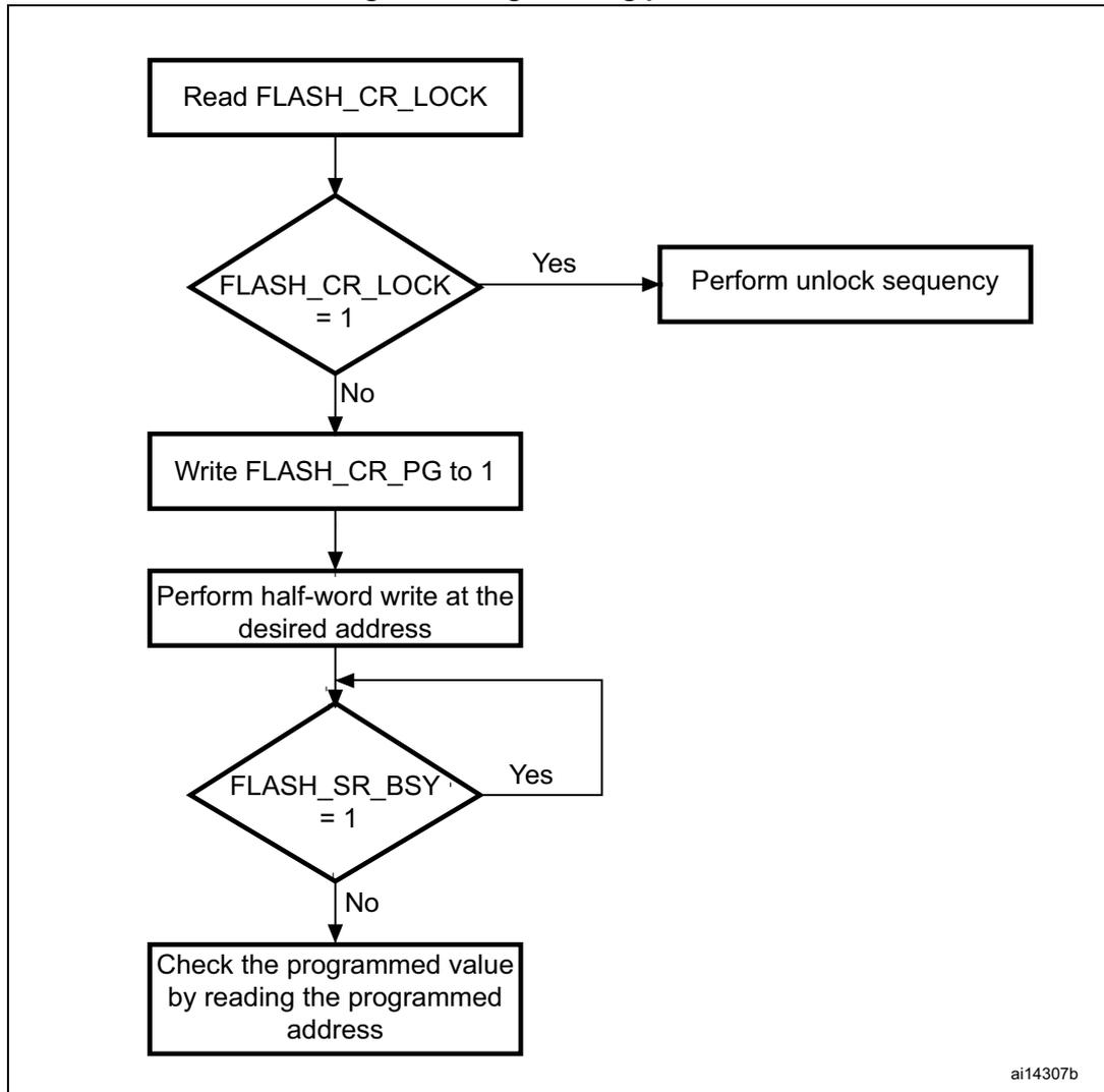
graph TD; A[Read FLASH_CR_LOCK] --> B{FLASH_CR_LOCK = 1}; B -- Yes --> C[Perform unlock sequence]; B -- No --> D[Write FLASH_CR_PG to 1]; D --> E[Perform half-word write at the desired address]; E --> F{FLASH_SR_BSY = 1}; F -- Yes --> F; F -- No --> G[Check the programmed value by reading the programmed address];The flowchart illustrates the programming procedure. It begins with 'Read FLASH_CR_LOCK', followed by a decision 'FLASH_CR_LOCK = 1'. If 'Yes', it proceeds to 'Perform unlock sequence'. If 'No', it proceeds to 'Write FLASH_CR_PG to 1', then 'Perform half-word write at the desired address'. Next is a decision 'FLASH_SR_BSY = 1'. If 'Yes', it loops back to the entry point of the 'FLASH_SR_BSY = 1' decision. If 'No', it proceeds to 'Check the programmed value by reading the programmed address'.
ai14307b
The flash memory interface preliminarily reads the value at the addressed main flash memory location and checks that it has been erased. If not, the program operation is skipped and a warning is issued by the PGERR bit in FLASH_SR register (the only exception to this is when 0x0000 is programmed. In this case, the location is correctly programmed to 0x0000 and the PGERR bit is not set). If the addressed main flash memory location is write-protected by the FLASH_WRPR register, the program operation is skipped and a warning is issued by the WRPRERR bit in the FLASH_SR register. The end of the program operation is indicated by the EOP bit in the FLASH_SR register.
The main flash memory programming sequence in standard mode is as follows:
- 1. Check that no main flash memory operation is ongoing by checking the BSY bit in the FLASH_SR register.
- 2. Set the PG bit in the FLASH_CR register.
- 3. Perform the data write (half-word) at the desired address.
- 4. Wait until the BSY bit is reset in the FLASH_SR register.
- 5. Check the EOP flag in the FLASH_SR register (it is set when the programming operation has succeeded), and then clear it by software.
Note: The registers are not accessible in write mode when the BSY bit of the FLASH_SR register is set.
Flash memory erase
The flash memory can be erased page by page or completely (mass erase).
Page erase
To erase a page, the procedure below must be followed:
- 1. Check that no flash memory operation is ongoing by checking the BSY bit in the FLASH_SR register.
- 2. Set the PER bit in the FLASH_CR register.
- 3. Program the FLASH_AR register to select a page to erase.
- 4. Set the STRT bit in the FLASH_CR register (see below note).
- 5. Wait for the BSY bit to be reset.
- 6. Check the EOP flag in the FLASH_SR register (it is set when the erase operation has succeeded), and then clear it by software.
- 7. Clear the EOP flag.
Note: The software should start checking if the BSY bit equals '0' at least one CPU cycle after setting the STRT bit.
Figure 5. Flash memory Page Erase procedure
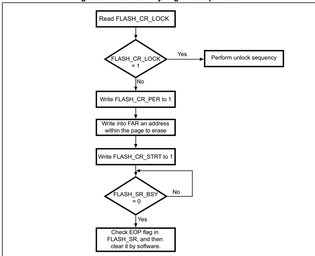
graph TD; A[Read FLASH_CR_LOCK] --> B{FLASH_CR_LOCK = 1}; B -- Yes --> C[Perform unlock sequence]; B -- No --> D[Write FLASH_CR_PER to 1]; D --> E[Write into FAR an address within the page to erase]; E --> F[Write FLASH_CR_STRT to 1]; F --> G{FLASH_SR_BSY = 0}; G -- No --> F; G -- Yes --> H[Check EOP flag in FLASH_SR, and then clear it by software.];The flowchart illustrates the Page Erase procedure. It begins with 'Read FLASH_CR_LOCK', followed by a decision 'FLASH_CR_LOCK = 1'. If 'Yes', it proceeds to 'Perform unlock sequence'. If 'No', it proceeds to 'Write FLASH_CR_PER to 1', then 'Write into FAR an address within the page to erase', and then 'Write FLASH_CR_STRT to 1'. A loop exists between 'Write FLASH_CR_STRT to 1' and a decision 'FLASH_SR_BSY = 0'. If 'No', it loops back to 'Write FLASH_CR_STRT to 1'. If 'Yes', it proceeds to 'Check EOP flag in FLASH_SR, and then clear it by software.'
Mass erase
The Mass erase command can be used to completely erase the user pages of the flash memory. The information block is unaffected by this procedure. The following sequence is recommended:
- 1. Check that no flash memory operation is ongoing by checking the BSY bit in the FLASH_SR register
- 2. Set the MER bit in the FLASH_CR register
- 3. Set the STRT bit in the FLASH_CR register (see below note)
- 4. Wait for the BSY bit to be reset
- 5. Check the EOP flag in the FLASH_SR register (it is set when the erase operation has succeeded), and then clear it by software.
- 6. Clear the EOP flag.
Note: The software must start checking if the BSY bit equals '0' at least one CPU cycle after setting the STRT bit.
Figure 6. Flash memory Mass Erase procedure
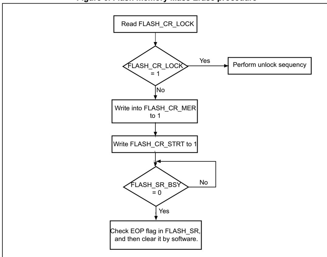
graph TD; A[Read FLASH_CR_LOCK] --> B{FLASH_CR_LOCK = 1}; B -- Yes --> C[Perform unlock sequence]; B -- No --> D[Write into FLASH_CR_MER to 1]; D --> E[Write FLASH_CR_STRT to 1]; E --> F{FLASH_SR_BSY = 0}; F -- No --> F; F -- Yes --> G[Check EOP flag in FLASH_SR, and then clear it by software.];The flowchart illustrates the Mass Erase procedure for flash memory. It begins with reading the FLASH_CR_LOCK register. A decision diamond checks if FLASH_CR_LOCK equals 1. If 'Yes', the procedure moves to 'Perform unlock sequence'. If 'No', it proceeds to 'Write into FLASH_CR_MER to 1', followed by 'Write FLASH_CR_STRT to 1'. Another decision diamond checks if FLASH_SR_BSY equals 0. If 'No', the process loops back to the entry point before this diamond. If 'Yes', the final step is 'Check EOP flag in FLASH_SR, and then clear it by software.'
Option byte programming
The option bytes are programmed differently from normal user addresses. The number of option bytes is limited to 6 (2 for write protection, 1 for readout protection, 1 for hardware configuration, and 2 for data storage). After unlocking the FPEC, the user has to authorize the programming of the option bytes by writing the same set of KEYS (KEY1 and KEY2) to the FLASH_OPTKEYR register (refer to Unlocking the flash memory for key values). Then, the OPTWRE bit in the FLASH_CR register is set by hardware and the user has to set the OPTPG bit in the FLASH_CR register and perform a half-word write operation at the desired flash memory address.
The value of the addressed option byte is first read to check it is really erased. If not, the program operation is skipped and a warning is issued by the PGERR bit in the FLASH_SR register. The end of the program operation is indicated by the EOP bit in the FLASH_SR register.
The LSB value is automatically complemented into the MSB before the programming operation starts. This guarantees that the option byte and its complement are always correct.
The sequence is as follows:
- • Check that no flash memory operation is ongoing by checking the BSY bit in the FLASH_SR register.
- • Unlock the OPTWRE bit in the FLASH_CR register.
- • Set the OPTPG bit in the FLASH_CR register
- • Write the data (half-word) to the desired address
- • Wait for the BSY bit to be reset.
- • Read the programmed value and verify.
When the flash memory read protection option is changed from protected to unprotected, a Mass Erase of the main flash memory is performed before reprogramming the read protection option. If the user wants to change an option other than the read protection option, then the mass erase is not performed. The erased state of the read protection option byte protects the flash memory.
Erase procedure
The option byte erase sequence (OPTERASE) is as follows:
- • Check that no flash memory operation is ongoing by reading the BSY bit in the FLASH_SR register.
- • Unlock the OPTWRE bit in the FLASH_CR register.
- • Set the OPTER bit in the FLASH_CR register.
- • Set the STRT bit in the FLASH_CR register.
- • Wait for BSY to reset.
- • Read the erased option bytes and verify.
4.3 Memory protection
The user area of the flash memory can be protected against read by untrusted code. The pages of the flash memory can also be protected against unwanted write due to loss of program counter contexts. The write-protection granularity is two pages.
4.3.1 Read protection
The read protection is activated by setting the RDP option byte and then, by applying a system reset to reload the new RDP option byte.
There are three levels of read protection from no protection (level 0) to maximum protection or no debug (level 2).
The flash memory is protected when the RDP option byte and its complement contain the pair of values shown in Table 8 .
Table 8. Flash memory read protection status
| RDP byte value | RDP complement value | Read protection level |
|---|---|---|
| 0xAA | 0x55 | Level 0 (ST production configuration) |
| Any value except 0xAA or 0xCC | Any value (not necessarily complementary) except 0x55 and 0x33 | Level 1 |
| 0xCC | 0x33 | Level 2 |
The system memory area is read accessible whatever the protection level. It is never accessible for program/erase operation
Level 0: no protection
Read, program, and erase operations into the main memory flash area are possible. The option bytes are also accessible by all operations.
Level 1: Read protection
This is the default protection level when RDP option byte is erased. It is defined as well when RDP value is at any value different from 0xAA and 0xCC, or even if the complement is not correct.
- • User mode: Code executing in user mode can access main memory flash and option bytes with all operations.
- • Debug, boot RAM, and bootloader modes: In debug mode or when code is running from boot RAM or bootloader, the main flash memory and the backup registers (RTC_BKPxR in the RTC) are totally inaccessible. In these modes, even a simple read access generates a bus error and a Hard Fault interrupt. The main memory is program/erase protected to prevent malicious or unauthorized users from reprogramming any of the user code with a dump routine. Any attempted program/erase operation sets the PGERR flag of Flash status register (FLASH_SR). When the RDP is reprogrammed to the value 0xAA to move back to Level 0, a mass erase of main memory flash is performed and the backup registers (RTC_BKPxR in the RTC) are reset.
Level 2: No debug
In this level, the protection level 1 is ensured. In addition, the Cortex ® -M4 debug capabilities are disabled. Consequently, the debug port, the boot from RAM (boot RAM mode) and the boot from the system memory (bootloader mode) are no more available. In user execution mode, all operations are allowed on the Main flash memory. On the contrary, only read and program operations can be performed on the option bytes.
Option bytes cannot be erased. Moreover, the RDP bytes cannot be programmed. Thus, the level 2 cannot be removed at all: it is an irreversible operation. When attempting to program the RDP byte, the protection error flag WRPRTERR is set in the FLASH_SR register, and an interrupt can be generated.
Note: The debug feature is also disabled under reset.
STMicroelectronics is not able to perform analysis on defective parts on which the level 2 protection has been set.
Table 9. Access status versus protection level and execution modes
| Area | Protection level | User execution | Debug ootFromRam/ BootFromLoader | ||||
|---|---|---|---|---|---|---|---|
| Read | Write | Erase | Read | Write | Erase | ||
| Main Flash memory | 1 | Yes | Yes | Yes | No | No | No (3) |
| 2 | Yes | Yes | Yes | N/A (1) | N/A (1) | N/A (1) | |
| System memory (2) | 1 | Yes | No | No | Yes | No | No |
| 2 | Yes | No | No | N/A (1) | N/A (1) | N/A (1) | |
| Option bytes | 1 | Yes | Yes (3) | Yes | Yes | Yes (3) | Yes |
| 2 | Yes | Yes (4) | No | N/A (1) | N/A (1) | N/A (1) | |
| Backup registers | 1 | Yes | Yes | N/A | No | No | No (5) |
| 2 | Yes | Yes | N/A | N/A (1) | N/A (1) | N/A (1) | |
- 1. When the protection level 2 is active, the debug port, the boot from RAM and the boot from system memory are disabled.
- 2. The system memory is only read-accessible, whatever the protection level (0, 1 or 2) and execution mode.
- 3. The main flash memory is erased when the RDP option byte is programmed with all level protections disabled (0xAA).
- 4. All option bytes can be programmed, except the RDP byte.
- 5. The backup registers are erased only when RDP changes from level 1 to level 0.
Changing read protection level
It is easy to move from level 0 to level 1 by changing the value of the RDP byte to any value (except 0xCC). By programming the 0xCC value in the RDP byte, it is possible to go to level 2 either directly from level 0 or from level 1. On the contrary, the change to level 0 (no protection) is not possible without a main flash memory Mass Erase operation. This Mass Erase is generated as soon as 0xAA is programmed in the RDP byte.
Note: When the Mass Erase command is used, the backup registers (RTC_BKPxR in the RTC) are also reset.
To validate the protection level change, the option bytes must be reloaded through the OBL_LAUNCH bit in Flash control register.
4.3.2 Write protection
The write protection is implemented with a granularity of 2 pages. It is activated by configuring the WRP[1:0] option bytes, and then by reloading them by setting the OBL_LAUNCH bit in the FLASH_CR register.
If a program or an erase operation is performed on a protected, the flash memory returns a WRPRERR protection error flag in the Flash memory Status Register (FLASH_SR).
Write unprotection
To disable the write protection, two application cases are provided:
- • Case 1: Read protection disabled after the write unprotection:
- – Erase the entire option byte area by using the OPTER bit in the Flash memory control register (FLASH_CR).
- – Program the code 0xAA in the RDP byte to unprotect the memory. This operation forces a Mass Erase of the main flash memory.
- – Set the OBL_LAUNCH bit in the Flash control register (FLASH_CR) to reload the option bytes (and the new WRP[3:0] bytes), and to disable the write protection.
- • Case 2: Read protection maintained active after the write unprotection, useful for in-application programming with a user bootloader:
- – Erase the entire option byte area by using the OPTER bit in the Flash memory control register (FLASH_CR).
- – Set the OBL_LAUNCH bit in the Flash control register (FLASH_CR) to reload the option bytes (and the new WRP[3:0] bytes), and to disable the write protection.
4.3.3 Option byte block write protection
The option bytes are always read-accessible and write-protected by default. To gain write access (Program/Erase) to the option bytes, a sequence of keys (same as for lock) has to be written into the OPTKEYR. A correct sequence of keys gives write access to the option bytes and this is indicated by OPTWRE in the FLASH_CR register being set. Write access can be disabled by resetting the bit through software.
4.4 Flash interrupts
Table 10. Flash interrupt request
| Interrupt event | Event flag | Enable control bit |
|---|---|---|
| End of operation | EOP | EOPIE |
| Write protection error | WRPRERR | ERRIE |
| Programming error | PGERR | ERRIE |
4.5 Flash register description
The flash memory registers must be accessed by 32-bit words (half-word and byte accesses are not allowed).
4.5.1 Flash access control register (FLASH_ACR)
Address offset: 0x00
Reset value: 0x0000 0030
| 31 | 30 | 29 | 28 | 27 | 26 | 25 | 24 | 23 | 22 | 21 | 20 | 19 | 18 | 17 | 16 |
|---|---|---|---|---|---|---|---|---|---|---|---|---|---|---|---|
| Res. | Res. | Res. | Res. | Res. | Res. | Res. | Res. | Res. | Res. | Res. | Res. | Res. | Res. | Res. | Res. |
| 15 | 14 | 13 | 12 | 11 | 10 | 9 | 8 | 7 | 6 | 5 | 4 | 3 | 2 | 1 | 0 |
| Res. | Res. | Res. | Res. | Res. | Res. | Res. | Res. | Res. | Res. | PRFT BS | PRFT BE | HLF CYA | LATENCY[2:0] | ||
| r | rw | rw | rw | rw | rw | ||||||||||
Bits 31:6 Reserved, must be kept at reset value.
Bit 5 PRFTBS : Prefetch buffer status
This bit provides the status of the prefetch buffer.
0: Prefetch buffer is disabled
1: Prefetch buffer is enabled
Bit 4 PRFTBE : Prefetch buffer enable
0: Prefetch is disabled
1: Prefetch is enabled
Bit 3 HLFCYA : Flash half cycle access enable
0: Half cycle is disabled
1: Half cycle is enabled
Bits 2:0 LATENCY[2:0] : Latency
These bits represent the ratio of the HCLK period to the Flash access time.
000: Zero wait state, if \( 0 < HCLK \leq 24 \) MHz
001: One wait state, if \( 24 \) MHz \( < HCLK \leq 48 \) MHz
010: Two wait states, if \( 48 < HCLK \leq 72 \) MHz
4.5.2 Flash key register (FLASH_KEYR)
Address offset: 0x04
Reset value: 0xXXXX XXXX
These bits are all write-only and return a 0 when read.
| 31 | 30 | 29 | 28 | 27 | 26 | 25 | 24 | 23 | 22 | 21 | 20 | 19 | 18 | 17 | 16 |
|---|---|---|---|---|---|---|---|---|---|---|---|---|---|---|---|
| FKEYR[31:16] | |||||||||||||||
| w | w | w | w | w | w | w | w | w | w | w | w | w | w | w | w |
| 15 | 14 | 13 | 12 | 11 | 10 | 9 | 8 | 7 | 6 | 5 | 4 | 3 | 2 | 1 | 0 |
| FKEYR[15:0] | |||||||||||||||
| w | w | w | w | w | w | w | w | w | w | w | w | w | w | w | w |
Bits 31:0 FKEYR : Flash key
These bits represent the keys to unlock the Flash.
4.5.3 Flash option key register (FLASH_OPTKEYR)
Address offset: 0x08
Reset value: 0xXXXX XXXX
All the register bits are write-only and return a 0 when read.
| 31 | 30 | 29 | 28 | 27 | 26 | 25 | 24 | 23 | 22 | 21 | 20 | 19 | 18 | 17 | 16 |
|---|---|---|---|---|---|---|---|---|---|---|---|---|---|---|---|
| OPTKEYR[31:16] | |||||||||||||||
| w | w | w | w | w | w | w | w | w | w | w | w | w | w | w | w |
| 15 | 14 | 13 | 12 | 11 | 10 | 9 | 8 | 7 | 6 | 5 | 4 | 3 | 2 | 1 | 0 |
| OPTKEYR[15:0] | |||||||||||||||
| w | w | w | w | w | w | w | w | w | w | w | w | w | w | w | w |
Bits 31:0 OPTKEYR : Option byte key
These bits represent the keys to unlock the OPTWRE.
4.5.4 Flash status register (FLASH_SR)
Address offset: 0x0C
Reset value: 0x0000 0000
| 31 | 30 | 29 | 28 | 27 | 26 | 25 | 24 | 23 | 22 | 21 | 20 | 19 | 18 | 17 | 16 |
|---|---|---|---|---|---|---|---|---|---|---|---|---|---|---|---|
| Res. | Res. | Res. | Res. | Res. | Res. | Res. | Res. | Res. | Res. | Res. | Res. | Res. | Res. | Res. | Res. |
| 15 | 14 | 13 | 12 | 11 | 10 | 9 | 8 | 7 | 6 | 5 | 4 | 3 | 2 | 1 | 0 |
| Res. | Res. | Res. | Res. | Res. | Res. | Res. | Res. | Res. | Res. | EOP | WRPRT ERR | Res. | PG ERR | Res. | BSY |
| rw | rw | rw | r |
Bits 31:6 Reserved, must be kept at reset value.
Bit 5 EOP : End of operation
Set by hardware when a Flash operation (programming / erase) is completed.
Reset by writing a 1
Note: EOP is asserted at the end of each successful program or erase operation
Bit 4 WRPRTERR : Write protection error
Set by hardware when programming a write-protected address of the Flash memory.
Reset by writing 1.
Bit 3 Reserved, must be kept at reset value.
Bit 2 PGERR : Programming error
Set by hardware when an address to be programmed contains a value different from '0xFFFF' before programming.
Reset by writing 1.
Note: The STRT bit in the FLASH_CR register should be reset before starting a programming operation.
Bit 1 Reserved, must be kept at reset value.
Bit 0 BSY : Busy
This indicates that a Flash operation is in progress. This is set on the beginning of a Flash operation and reset when the operation finishes or when an error occurs.
4.5.5 Flash control register (FLASH_CR)
Address offset: 0x10
Reset value: 0x0000 0080
| 31 | 30 | 29 | 28 | 27 | 26 | 25 | 24 | 23 | 22 | 21 | 20 | 19 | 18 | 17 | 16 |
|---|---|---|---|---|---|---|---|---|---|---|---|---|---|---|---|
| Res. | Res. | Res. | Res. | Res. | Res. | Res. | Res. | Res. | Res. | Res. | Res. | Res. | Res. | Res. | Res. |
| 15 | 14 | 13 | 12 | 11 | 10 | 9 | 8 | 7 | 6 | 5 | 4 | 3 | 2 | 1 | 0 |
| Res. | Res. | OBL_LAUNCH | EOPIE | Res. | ERRIE | OPTWRE | Res. | LOCK | STRT | OPTER | OPTPG | Res. | MER | PER | PG |
| rw | rw | rw | rw | rw | rw | rw | rw | rw | rw | rw |
Bits 31:14 Reserved, must be kept at reset value.
Bit 13 OBL_LAUNCH : Force option byte loading
When set to 1, this bit forces the option byte reloading. This operation generates a system reset.
0: Inactive
1: Active
Bit 12 EOPIE : End of operation interrupt enable
This bit enables the interrupt generation when the EOP bit in the FLASH_SR register goes to 1.
0: Interrupt generation disabled
1: Interrupt generation enabled
Bit 11 Reserved, must be kept at reset value.
Bit 10 ERRIE : Error interrupt enable
This bit enables the interrupt generation on an error when PGERR / WRPRERR are set in the FLASH_SR register.
0: Interrupt generation disabled
1: Interrupt generation enabled
Bit 9 OPTWRE : Option bytes write enable
When set, the option bytes can be programmed. This bit is set on writing the correct key sequence to the FLASH_OPTKEYR register.
This bit can be reset by software
Bit 8 Reserved, must be kept at reset value.
Bit 7 LOCK : LockWrite to 1 only. When it is set, it indicates that the Flash is locked. This bit is reset by hardware after detecting the unlock sequence.
In the event of unsuccessful unlock operation, this bit remains set until the next reset.
Bit 6 STR : StartThis bit triggers an ERASE operation when set. This bit is set only by software and reset when the BSY bit is reset.
Bit 5 OPTER : Option byte eraseOption byte erase chosen.
Bit 4 OPTPG : Option byte programmingOption byte programming chosen.
Bit 3 Reserved, must be kept at reset value.
Bit 2 MER : Mass eraseErase of all user pages chosen.
Bit 1 PER : Page erasePage Erase chosen.
Bit 0 PG : ProgrammingFlash programming chosen.
4.5.6 Flash address register (FLASH_AR)
Address offset: 0x14
Reset value: 0x0000 0000
This register is updated by hardware with the currently/last used address. For Page Erase operations, this should be updated by software to indicate the chosen page.

| 31 | 30 | 29 | 28 | 27 | 26 | 25 | 24 | 23 | 22 | 21 | 20 | 19 | 18 | 17 | 16 |
| FAR[31:16] | |||||||||||||||
| w | w | w | w | w | w | w | w | w | w | w | w | w | w | w | w |
| 15 | 14 | 13 | 12 | 11 | 10 | 9 | 8 | 7 | 6 | 5 | 4 | 3 | 2 | 1 | 0 |
| FAR[15:0] | |||||||||||||||
| w | w | w | w | w | w | w | w | w | w | w | w | w | w | w | w |
Chooses the address to program when programming is selected, or a page to erase when Page Erase is selected.
Note: Write access to this register is blocked when the BSY bit in the FLASH_SR register is set.
4.5.7 Option byte register (FLASH_OBR)
Address offset 0x1C
Reset value: 0xXXXX XX0X
It contains the level protection notifications, error during load of option bytes and user options.
The reset value of this register depends on the value programmed in the option byte and the OPTERR bit reset value depends on the comparison of the option byte and its complement during the option byte loading phase.
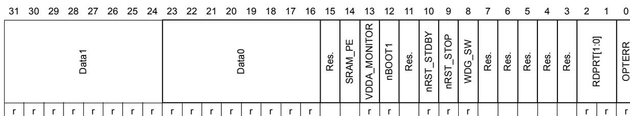
| 31 | 30 | 29 | 28 | 27 | 26 | 25 | 24 | 23 | 22 | 21 | 20 | 19 | 18 | 17 | 16 | 15 | 14 | 13 | 12 | 11 | 10 | 9 | 8 | 7 | 6 | 5 | 4 | 3 | 2 | 1 | 0 |
| Data1 | Data0 | Res. | SRAM_PE | VDDA_MONITOR | nBOOT1 | Res. | nRST_STDBY | nRST_STOP | WDG_SW | Res. | Res. | Res. | Res. | Res. | RDPRT[1:0] | OPTERR | |||||||||||||||
| r | r | r | r | r | r | r | r | r | r | r | r | r | r | r | r | r | r | r | r | r | r | r | r | ||||||||
Bits 31:24 Data1
Bits 23:16 Data0
Bits 15:8 OBR : User Option Byte
Bit 15: Reserved, must be kept at reset value.
Bit 14: SRAM_PE.
Bit 13: VDDA_MONITOR
Bit 12: nBOOT1
Bit 11: Reserved, must be kept at reset value.
Bit 10: nRST_STDBY
Bit 9: nRST_STOP
Bit 8: WDG_SW
Bits 7:3 Reserved, must be kept at reset value.
Bits 2:1 RDPRT[1:0] : Read protection Level status
00: Read protection Level 0 is enabled (ST production set up)
01: Read protection Level 1 is enabled
10: Reserved
11: Read protection Level 2 is enabled
Note: These bits are read-only.
Bit 0 OPTERR : Option byte Load error
When set, this indicates that the loaded option byte and its complement do not match. The corresponding byte and its complement are read as 0xFF in the FLASH_OBR or FLASH_WRPR register.
Note: This bit is read-only.
4.5.8 Write protection register (FLASH_WRPR)
Address offset: 0x20
Reset value: 0xFFFF FFFF
| 31 | 30 | 29 | 28 | 27 | 26 | 25 | 24 | 23 | 22 | 21 | 20 | 19 | 18 | 17 | 16 |
|---|---|---|---|---|---|---|---|---|---|---|---|---|---|---|---|
| WRP[31:16] | |||||||||||||||
| r | r | r | r | r | r | r | r | r | r | r | r | r | r | r | r |
| 15 | 14 | 13 | 12 | 11 | 10 | 9 | 8 | 7 | 6 | 5 | 4 | 3 | 2 | 1 | 0 |
| WRP[15:0] | |||||||||||||||
| r | r | r | r | r | r | r | r | r | r | r | r | r | r | r | r |
Bits 31:0 WRP : Write protect
This register contains the write-protection option bytes loaded by the OBL.
These bits are read-only.
4.6 Flash register map
Table 11. Flash interface - register map and reset values
| Offset | Register | 31 | 30 | 29 | 28 | 27 | 26 | 25 | 24 | 23 | 22 | 21 | 20 | 19 | 18 | 17 | 16 | 15 | 14 | 13 | 12 | 11 | 10 | 9 | 8 | 7 | 6 | 5 | 4 | 3 | 2 | 1 | 0 |
|---|---|---|---|---|---|---|---|---|---|---|---|---|---|---|---|---|---|---|---|---|---|---|---|---|---|---|---|---|---|---|---|---|---|
| 0x000 | FLASH_ACR | Res. | Res. | Res. | Res. | Res. | Res. | Res. | Res. | Res. | Res. | Res. | Res. | Res. | Res. | Res. | Res. | Res. | Res. | Res. | Res. | Res. | Res. | Res. | Res. | Res. | Res. | PRFTBS | PRFTBE | HLFCYA | LATENCY [2:0] | ||
| Reset value | 1 | 1 | 0 | 0 | 0 | 0 | |||||||||||||||||||||||||||
| 0x004 | FLASH_KEYR | FKEYR[31:0] | |||||||||||||||||||||||||||||||
| Reset value | x | x | x | x | x | x | x | x | x | x | x | x | x | x | x | x | x | x | x | x | x | x | x | x | x | x | x | x | x | x | x | x | |
| 0x008 | FLASH_OPTKEYR | OPTKEYR[31:0] | |||||||||||||||||||||||||||||||
| Reset value | x | x | x | x | x | x | x | x | x | x | x | x | x | x | x | x | x | x | x | x | x | x | x | x | x | x | x | x | x | x | x | x | |
| 0x00C | FLASH_SR | Res. | Res. | Res. | Res. | Res. | Res. | Res. | Res. | Res. | Res. | Res. | Res. | Res. | Res. | Res. | Res. | Res. | Res. | Res. | Res. | Res. | Res. | Res. | Res. | Res. | Res. | EOP | WRPRTERR | Res. | PGERR | Res. | BSY |
| Reset value | 0 | 0 | 0 | 0 | |||||||||||||||||||||||||||||
| 0x010 | FLASH_CR | Res. | Res. | Res. | Res. | Res. | Res. | Res. | Res. | Res. | Res. | Res. | Res. | Res. | Res. | Res. | Res. | Res. | Res. | OBL_LAUNCH | EOPIE | Res. | ERRIE | OPTWRE | Res. | LOCK | STRT | OPTER | OPTPG | Res. | MER | PER | PG |
| Reset value | 0 | 0 | 0 | 0 | 1 | 0 | 0 | 0 | 0 | 0 | 0 | ||||||||||||||||||||||
| 0x014 | FLASH_AR | FAR[31:0] | |||||||||||||||||||||||||||||||
| Reset value | 0 | 0 | 0 | 0 | 0 | 0 | 0 | 0 | 0 | 0 | 0 | 0 | 0 | 0 | 0 | 0 | 0 | 0 | 0 | 0 | 0 | 0 | 0 | 0 | 0 | 0 | 0 | 0 | 0 | 0 | 0 | 0 | |
Table 11. Flash interface - register map and reset values (continued)
| Offset | Register | 31 | 30 | 29 | 28 | 27 | 26 | 25 | 24 | 23 | 22 | 21 | 20 | 19 | 18 | 17 | 16 | 15 | 14 | 13 | 12 | 11 | 10 | 9 | 8 | 7 | 6 | 5 | 4 | 3 | 2 | 1 | 0 |
|---|---|---|---|---|---|---|---|---|---|---|---|---|---|---|---|---|---|---|---|---|---|---|---|---|---|---|---|---|---|---|---|---|---|
| 0x01C | FLASH_OBR | Data1 | Data0 | Res. | SRAM_PE | VDDA_MONITOR | nBOOT1 | Res. | nRST_STDBY | nRST_STOP | WDG_SW | ||||||||||||||||||||||
| Reset value | x | x | x | x | x | x | x | x | x | x | x | x | x | x | x | x | x | x | x | x | x | x | x | x | |||||||||
| 0x020 | FLASH_WRP | WRP[31:0] | |||||||||||||||||||||||||||||||
| Reset value | 1 | 1 | 1 | 1 | 1 | 1 | 1 | 1 | 1 | 1 | 1 | 1 | 1 | 1 | 1 | 1 | 1 | 1 | 1 | 1 | 1 | 1 | 1 | 1 | 1 | 1 | 1 | 1 | 1 | 1 | 1 | 1 | |
Refer to Section 3.2 on page 53 for the register boundary addresses.