3. System and memory overview
3.1 System architecture
The STM32F302xB/C/D/E, STM32F358xC and STM32F398xE main system consists of:
- • Five masters:
- – Cortex ® -M4 core I-bus
- – Cortex ® -M4 core D-bus
- – Cortex ® -M4 core S-bus
- – GP-DMA1 and GP-DMA2 (general-purpose DMAs)
- • Seven (eight in STM32F303xDxE and STM32F398xE) slaves:
- – Internal Flash memory on the DCode
- – Internal flash memory on ICode
- – Up to internal 40-Kbyte SRAM
- – Internal 8-Kbyte CCM SRAM (16-Kbyte CCM SRAM for STM32F303xE and STM32F398xE)
- – FMC in STM32F303xDxE and STM32F398xE
- – AHB to APBx (APB1 or APB2), which connect all the APB peripherals
- – AHB dedicated to GPIO ports
- – ADCs 1, 2, 3 and 4.
The STM32F303x6/8 and STM32F328x8 main system consists of:
- • Four masters:
- – Cortex ® -M4 core I-bus
- – Cortex ® -M4 core D-bus
- – Cortex ® -M4 core S-bus
- – DMA1 (general-purpose DMA)
- • Seven slaves:
- – Internal flash memory on the DCode
- – Internal flash memory on ICode
- – Up to 12-Kbyte internal SRAM
- – Internal 4-Kbyte CCM SRAM
- – AHB to APBx (APB1 or APB2), which connect all the APB peripherals
- – AHB dedicated to GPIO ports
- – ADCs 1 and 2
The interconnection uses a multilayer AHB bus architecture as shown in figures 1 to 3.
Figure 1. STM32F303xB/C and STM32F358xC system architecture
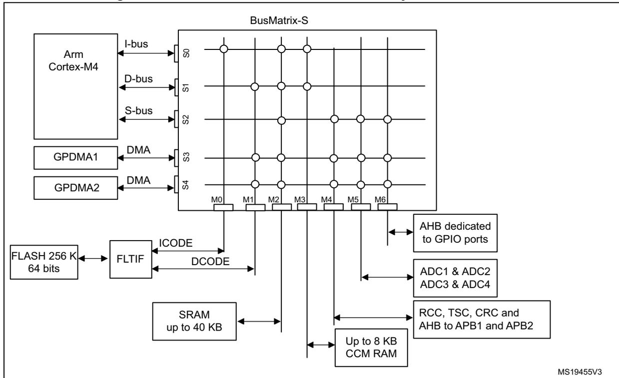
Figure 1 illustrates the system architecture for STM32F303xB/C and STM32F358xC. At the center is the BusMatrix-S , which connects various system components. The Arm Cortex-M4 is connected via its I-bus, D-bus, and S-bus. Two DMA controllers, GPDMA1 and GPDMA2 , are connected via their DMA interfaces. The FLASH 256 K 64 bits is connected through an FLTIF block, which provides ICODE and DCODE signals. On the slave side, the matrix connects to SRAM up to 40 KB , Up to 8 KB CCM RAM , AHB dedicated to GPIO ports , ADC1 & ADC2 , ADC3 & ADC4 , and RCC, TSC, CRC and AHB to APB1 and APB2 . The matrix has 7 master ports (M0-M6) and 7 slave ports (S0-S6). Reference: MS19455V3.
Figure 2. STM32F303x6/8 and STM32F328x8 system architecture
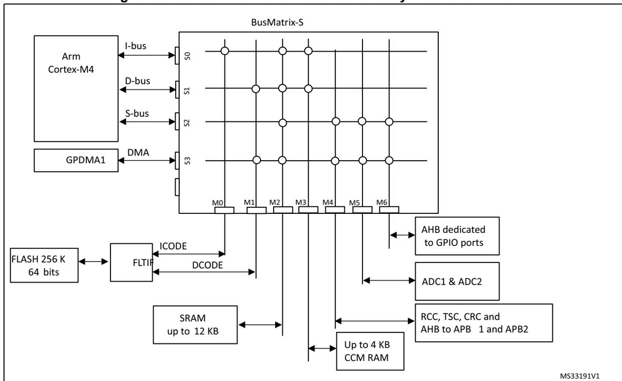
Figure 2 illustrates the system architecture for STM32F303x6/8 and STM32F328x8. It features a central BusMatrix-S connecting system components. The Arm Cortex-M4 is connected via its I-bus, D-bus, and S-bus. GPDMA1 is connected via its DMA interface. The FLASH 256 K 64 bits is connected through an FLTIF block, providing ICODE and DCODE signals. On the slave side, the matrix connects to SRAM up to 12 KB , Up to 4 KB CCM RAM , AHB dedicated to GPIO ports , ADC1 & ADC2 , and RCC, TSC, CRC and AHB to APB1 and APB2 . The matrix has 7 master ports (M0-M6) and 7 slave ports (S0-S6). Reference: MS33191V1.
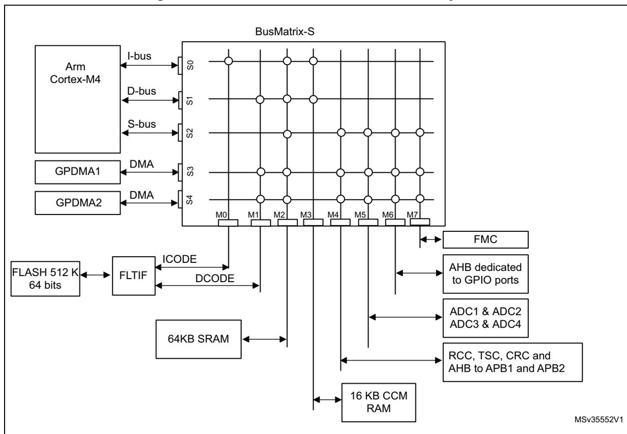
Figure 3. STM32F303xDxE and STM32F398xE system architecture
3.1.1 S0: I-bus
This bus connects the instruction bus of the Cortex ® -M4 core to the BusMatrix. This bus is used by the core to fetch instructions. The targets of this bus are the internal Flash memory, the SRAM and the CCM SRAM.
3.1.2 S1: D-bus
This bus connects the DCode bus (literal load and debug access) of the Cortex ® -M4 core to the BusMatrix. The targets of this bus are the internal Flash memory, the SRAM and the CCM SRAM.
3.1.3 S2: S-bus
This bus connects the system bus of the Cortex ® -M4 core to the BusMatrix. This bus is used to access data located in the peripheral or SRAM area. The targets of this bus are the SRAM, the AHB to APB1/APB2 bridges, the AHB IO port and the ADC.
3.1.4 S3, S4: DMA-bus
This bus connects the AHB master interface of the DMA to the BusMatrix, which manages the access of different Masters to flash, SRAM, and peripherals.
3.1.5 BusMatrix
The BusMatrix manages the access arbitration between Masters. The arbitration uses a Round Robin algorithm. The BusMatrix is composed of five masters (CPU AHB, System bus, DCode bus, ICode bus, DMA1/2 bus) and seven slaves (FLITF, SRAM, AHB2GPIO and AHB2APB1/2 bridges, and ADC).
AHB/APB bridges
The two AHB/APB bridges provide full synchronous connections between the AHB and the two APB buses. APB1 is limited to 36 MHz. APB2 operates at full speed (72 MHz).
Refer to Section 3.2: Memory organization on page 53 for the address mapping of the peripherals connected to this bridge.
After each device reset, all peripheral clocks are disabled (except for the SRAM and FLITF). Before using a peripheral the user has to enable its clock in the RCC_AHBENR, RCC_APB2ENR or RCC_APB1ENR register.
When a 16- or 8-bit access is performed on an APB register, the access is transformed into a 32-bit access: the bridge duplicates the 16- or 8-bit data to feed the 32-bit vector.
3.2 Memory organization
3.2.1 Introduction
Program memory, data memory, registers and I/O ports are organized within the same linear 4-Gbyte address space.
The bytes are coded in memory in Little Endian format. The lowest numbered byte in a word is considered the word's least significant byte and the highest numbered byte the most significant.
The addressable memory space is divided into eight main blocks, of 512 Mbytes each.
3.2.2 Memory map and register boundary addresses
All the memory map areas that are not allocated to on-chip memories and peripherals are considered “Reserved”. For the detailed mapping of available memory and register areas, refer to the following table.
The following table gives the boundary addresses of the peripherals available in the devices.
Table 2. STM32F303xB/C and STM32F358xC peripheral register boundary addresses (1)
| Bus | Boundary address | Size (bytes) | Peripheral | Peripheral register map |
|---|---|---|---|---|
| AHB3 | 0x5000 0400 - 0x5000 07FF | 1 K | ADC3 - ADC4 | Section 15.7 on page 416 |
| 0x5000 0000 - 0x5000 03FF | 1 K | ADC1 - ADC2 | ||
| - | 0x4800 1800 - 0x4FFF FFFF | ~132 M | Reserved | - |
| AHB2 | 0x4800 1400 - 0x4800 17FF | 1 K | GPIOF | Section 11.4.12 on page 246 |
| 0x4800 1000 - 0x4800 13FF | 1 K | GPIOE | ||
| 0x4800 0C00 - 0x4800 0FFF | 1 K | GPIO D | ||
| 0x4800 0800 - 0x4800 0BFF | 1 K | GPIOC | ||
| 0x4800 0400 - 0x4800 07FF | 1 K | GPIOB | ||
| 0x4800 0000 - 0x4800 03FF | 1 K | GPIOA | ||
| - | 0x4002 4400 - 0x47FF FFFF | ~128 M | Reserved | |
| AHB1 | 0x4002 4000 - 0x4002 43FF | 1 K | TSC | Section 19.6.11 on page 510 |
| 0x4002 3400 - 0x4002 3FFF | 3 K | Reserved | - | |
| 0x4002 3000 - 0x4002 33FF | 1 K | CRC | Section 6.4.6 on page 96 | |
| 0x4002 2400 - 0x4002 2FFF | 3 K | Reserved | - | |
| 0x4002 2000 - 0x4002 23FF | 1 K | Flash interface | Section 4.6 on page 85 | |
| 0x4002 1400 - 0x4002 1FFF | 3 K | Reserved | - | |
| 0x4002 1000 - 0x4002 13FF | 1 K | RCC | Section 9.4.14 on page 168 | |
| 0x4002 0800 - 0x4002 0FFF | 2 K | Reserved | - | |
| 0x4002 0400 - 0x4002 07FF | 1 K | DMA2 | Section 13.6.7 on page 288 | |
| 0x4002 0000 - 0x4002 03FF | 1 K | DMA1 | ||
| - | 0x4001 8000 - 0x4001 FFFF | 32 K | Reserved | - |
Table 2. STM32F303xB/C and STM32F358xC peripheral register boundary addresses (1) (continued)
| Bus | Boundary address | Size (bytes) | Peripheral | Peripheral register map |
|---|---|---|---|---|
| APB2 | 0x4001 4C00 - 0x4001 7FFF | 13 K | Reserved | - |
| 0x4001 4800 - 0x4001 4BFF | 1 K | TIM17 | Section 23.6.18 on page 768 | |
| 0x4001 4400 - 0x4001 47FF | 1 K | TIM16 | ||
| 0x4001 4000 - 0x4001 43FF | 1 K | TIM15 | Section 23.5.19 on page 748 | |
| 0x4001 3C00 - 0x4001 3FFF | 1 K | Reserved | - | |
| 0x4001 3800 - 0x4001 3BFF | 1 K | USART1 | Section 29.8.12 on page 959 | |
| 0x4001 3400 - 0x4001 37FF | 1 K | TIM8 | Section 20.4.27 on page 605 | |
| 0x4001 3000 - 0x4001 33FF | 1 K | SPI1 | Section 30.9.10 on page 1018 | |
| 0x4001 2C00 - 0x4001 2FFF | 1 K | TIM1 | Section 20.4.27 on page 605 | |
| 0x4001 0800 - 0x4001 2BFF | 9 K | Reserved | - | |
| 0x4001 0400 - 0x4001 07FF | 1 K | EXTI | Section 14.3.13 on page 308 | |
| 0x4001 0000 - 0x4001 03FF | 1 K | SYSCFG + COMP + OPAMP | Section 12.1.10 on page 262
, Section 17.5.8 on page 470 , Section 18.4.5 on page 492 | |
| - | 0x4000 7800 - 0x4000 FFFF | 34 K | Reserved | - |
Table 2. STM32F303xB/C and STM32F358xC peripheral register boundary addresses (1) (continued)
| Bus | Boundary address | Size (bytes) | Peripheral | Peripheral register map |
|---|---|---|---|---|
| APB1 | 0x4000 7400 - 0x4000 77FF | 1 K | DAC1 | Section 16.10.15 on page 444 |
| 0x4000 7000 - 0x4000 73FF | 1 K | PWR | Section 7.4.3 on page 111 | |
| 0x4000 6C00 - 0x4000 6FFF | 1 K | Reserved | - | |
| 0x4000 6800 - 0x4000 6BFF | 1 K | Reserved | - | |
| 0x4000 6400 - 0x4000 67FF | 1 K | bxCAN | Section 31.9.5 on page 1058 | |
| 0x4000 6000 - 0x4000 63FF | 1 K | USB SRAM 512 bytes | Section 32.6.3 on page 1093 | |
| 0x4000 5C00 - 0x4000 5FFF | 1 K | USB device FS | ||
| 0x4000 5800 - 0x4000 5BFF | 1 K | I2C2 | Section 28.9.12 on page 893 | |
| 0x4000 5400 - 0x4000 57FF | 1 K | I2C1 | ||
| 0x4000 5000 - 0x4000 53FF | 1 K | UART5 | Section 29.8.12 on page 959 | |
| 0x4000 4C00 - 0x4000 4FFF | 1 K | UART4 | ||
| 0x4000 4800 - 0x4000 4BFF | 1 K | USART3 | ||
| 0x4000 4400 - 0x4000 47FF | 1 K | USART2 | ||
| 0x4000 4000 - 0x4000 43FF | 1 K | I2S3ext | Section 30.9.10 on page 1018 | |
| 0x4000 3C00 - 0x4000 3FFF | 1 K | SPI3/I2S3 | ||
| 0x4000 3800 - 0x4000 3BFF | 1 K | SPI2/I2S2 | ||
| 0x4000 3400 - 0x4000 37FF | 1 K | I2S2ext | ||
| 0x4000 3000 - 0x4000 33FF | 1 K | IWDG | Section 25.4.6 on page 779 | |
| 0x4000 2C00 - 0x4000 2FFF | 1 K | WWDG | Section 26.5.4 on page 785 | |
| 0x4000 2800 - 0x4000 2BFF | 1 K | RTC | Section 27.6.20 on page 827 | |
| - | 0x4000 1800 - 0x4000 27FF | 4 K | Reserved | - |
| APB1 | 0x4000 1400 - 0x4000 17FF | 1 K | TIM7 | Section 22.4.9 on page 690 |
| 0x4000 1000 - 0x4000 13FF | 1 K | TIM6 | ||
| 0x4000 0C00 - 0x4000 0FFF | 1 K | Reserved | - | |
| 0x4000 0800 - 0x4000 0BFF | 1 K | TIM4 | Section 21.4.22 on page 676 | |
| 0x4000 0400 - 0x4000 07FF | 1 K | TIM3 | ||
| 0x4000 0000 - 0x4000 03FF | 1 K | TIM2 | ||
| - | 0x2000 A000 - 3FFF FFFF | ~512 M | Reserved | - |
| - | 0x2000 0000 - 0x2000 9FFF | 40 K | SRAM | - |
| - | 0x1FFF F800 - 0x1FFF FFFF | 2 K | Option bytes | - |
| - | 0x1FFF D800 - 0x1FFF F7FF | 8 K | System memory | - |
| - | 0x1000 2000 - 0x1FFF D7FF | ~256 M | Reserved | - |
| - | 0x1000 0000 - 0x1000 1FFF | 8 K | CCM SRAM | - |
Table 2. STM32F303xB/C and STM32F358xC peripheral register boundary addresses (1) (continued)
| Bus | Boundary address | Size (bytes) | Peripheral | Peripheral register map |
|---|---|---|---|---|
| - | 0x0804 0000 - 0x0FFF FFFF | ~128 M | Reserved | - |
| - | 0x0800 0000 - 0x0803 FFFF | 256 K | Main Flash memory | - |
| - | 0x0004 0000 - 0x07FF FFFF | ~128 M | Reserved | - |
| - | 0x0000 000 - 0x0003 FFFF | 256 K | Main Flash memory, system memory or SRAM depending on BOOT configuration | - |
1. The gray color is used for reserved Flash memory addresses.
Table 3. STM32F303xD/E and STM32F398xE peripheral register boundary addresses (1)
| Bus | Boundary address | Size (bytes) | Peripheral | Peripheral register map |
|---|---|---|---|---|
| AHB4 | 0xA000 0400 - 0xA000 0FFF | 4 K | FMC control registers | Section 10.6.9: FMC register map |
| 0x8000 0400 - 0x9FFF FFFF | 512 M | FMC banks 3 and 4 | ||
| 0x6000 0000 - 0x7FFF FFFF | 512 M | FMC banks 1 and 2 | ||
| - | 0x5000 0800 - 0x5FFF FFFF | 384M | Reserved | - |
| AHB3 | 0x5000 0400 - 0x5000 07FF | 1 K | ADC3 - ADC4 | Section 15.7 on page 416 |
| 0x5000 0000 - 0x5000 03FF | 1 K | ADC1 - ADC2 | ||
| - | 0x4800 2000 - 0x4FFF FFFF | ~132 M | Reserved | - |
| AHB2 | 0x4800 1C00 - 0x4800 1FFF | 1 K | GPIOH | Section 11.4.12 on page 246 |
| 0x4800 1800 - 0x4800 1BFF | 1 K | GPIOG | ||
| 0x4800 1400 - 0x4800 17FF | 1 K | GPIOF | ||
| 0x4800 1000 - 0x4800 13FF | 1 K | GPIOE | ||
| 0x4800 0C00 - 0x4800 0FFF | 1 K | GPIO D | ||
| 0x4800 0800 - 0x4800 0BFF | 1 K | GPIOC | ||
| 0x4800 0400 - 0x4800 07FF | 1 K | GPIOB | ||
| 0x4800 0000 - 0x4800 03FF | 1 K | GPIOA | ||
| - | 0x4002 4400 - 0x47FF FFFF | ~128 M | Reserved |
Table 3. STM32F303xD/E and STM32F398xE peripheral register boundary addresses (1) (continued)
| Bus | Boundary address | Size (bytes) | Peripheral | Peripheral register map |
|---|---|---|---|---|
| AHB1 | 0x4002 4000 - 0x4002 43FF | 1 K | TSC | Section 19.6.11 on page 510 |
| 0x4002 3400 - 0x4002 3FFF | 3 K | Reserved | - | |
| 0x4002 3000 - 0x4002 33FF | 1 K | CRC | Section 6.4.6 on page 96 | |
| 0x4002 2400 - 0x4002 2FFF | 3 K | Reserved | - | |
| 0x4002 2000 - 0x4002 23FF | 1 K | Flash interface | Section 4.6 on page 85 | |
| 0x4002 1400 - 0x4002 1FFF | 3 K | Reserved | - | |
| 0x4002 1000 - 0x4002 13FF | 1 K | RCC | Section 9.4.14 on page 168 | |
| 0x4002 0800 - 0x4002 0FFF | 2 K | Reserved | - | |
| 0x4002 0400 - 0x4002 07FF | 1 K | DMA2 | Section 13.6.6 on page 288 | |
| 0x4002 0000 - 0x4002 03FF | 1 K | DMA1 | ||
| - | 0x4001 8000 - 0x4001 FFFF | 32 K | Reserved | - |
| APB2 | 0x4001 4C00 - 0x4001 4FFF | 1 K | Reserved | - |
| 0x4001 5400 - 0x4001 7FFF | 11 K | Reserved | - | |
| 0x4001 5000 - 0x4001 53FF | 1 K | TIM20 | Section 23.6.18 on page 768 | |
| 0x4001 4800 - 0x4001 4BFF | 1 K | TIM17 | ||
| 0x4001 4400 - 0x4001 47FF | 1 K | TIM16 | ||
| 0x4001 4000 - 0x4001 43FF | 1 K | TIM15 | Section 23.5.19 on page 748 | |
| 0x4001 3C00 - 0x4001 3FFF | 1 K | SPI4 | Section 30.9.10 on page 1018 | |
| 0x4001 3800 - 0x4001 3BFF | 1 K | USART1 | Section 29.8.12 on page 959 | |
| 0x4001 3400 - 0x4001 37FF | 1 K | TIM8 | Section 20.4.27 on page 605 | |
| 0x4001 3000 - 0x4001 33FF | 1 K | SPI1 | Section 30.9.10 on page 1018 | |
| 0x4001 2C00 - 0x4001 2FFF | 1 K | TIM1 | Section 20.4.27 on page 605 | |
| 0x4001 0800 - 0x4001 2BFF | 9 K | Reserved | - | |
| 0x4001 0400 - 0x4001 07FF | 1 K | EXTI | Section 14.3.13 on page 308 | |
| 0x4001 0000 - 0x4001 03FF | 1 K | SYSCFG + COMP + OPAMP | Section 12.1.10 on page 262
, Section 17.5.8 on page 470 , Section 18.4.5 on page 492 | |
| - | 0x4000 7C00 - 0x4000 FFFF | 33 K | Reserved | - |
Table 3. STM32F303xD/E and STM32F398xE peripheral register boundary addresses (1) (continued)
| Bus | Boundary address | Size (bytes) | Peripheral | Peripheral register map |
|---|---|---|---|---|
| APB1 | 0x4000 7800 - 0x4000 7BFF | 1 K | I2C3 | Section 28.9.12 on page 893 |
| 0x4000 7400 - 0x4000 77FF | 1 K | DAC1 | Section 16.10.15 on page 444 | |
| 0x4000 7000 - 0x4000 73FF | 1 K | PWR | Section 7.4.3 on page 111 | |
| 0x4000 6C00 - 0x4000 6FFF | 1 K | Reserved | - | |
| 0x4000 6800 - 0x4000 6BFF | 1 K | Reserved | - | |
| 0x4000 6400 - 0x4000 67FF | 1 K | bxCAN | Section 31.9.5 on page 1058 | |
| 0x4000 6000 - 0x4000 63FF | 1 K | USB/CAN SRAM | Section 32.6.3 on page 1093 | |
| 0x4000 5C00 - 0x4000 5FFF | 1 K | USB device FS | ||
| 0x4000 5800 - 0x4000 5BFF | 1 K | I2C2 | Section 28.9.1 on page 880 | |
| 0x4000 5400 - 0x4000 57FF | 1 K | I2C1 | ||
| 0x4000 5000 - 0x4000 53FF | 1 K | UART5 | Section 29.8.12 on page 959 | |
| 0x4000 4C00 - 0x4000 4FFF | 1 K | UART4 | ||
| 0x4000 4800 - 0x4000 4BFF | 1 K | USART3 | ||
| 0x4000 4400 - 0x4000 47FF | 1 K | USART2 | ||
| 0x4000 4000 - 0x4000 43FF | 1 K | I2S3ext | ||
| 0x4000 3C00 - 0x4000 3FFF | 1 K | SPI3/I2S3 | Section 30.9.10 on page 1018 | |
| 0x4000 3800 - 0x4000 3BFF | 1 K | SPI2/I2S2 | ||
| 0x4000 3400 - 0x4000 37FF | 1 K | I2S2ext | ||
| 0x4000 3000 - 0x4000 33FF | 1 K | IWDG | Section 25.4.6 on page 779 | |
| 0x4000 2C00 - 0x4000 2FFF | 1 K | WWDG | Section 26.5.4 on page 785 | |
| 0x4000 2800 - 0x4000 2BFF | 1 K | RTC | Section 27.6.20 on page 827 | |
| - | 0x4000 1800 - 0x4000 27FF | 4 K | Reserved | - |
| APB1 | 0x4000 1400 - 0x4000 17FF | 1 K | TIM7 | Section 22.4.9 on page 690 |
| 0x4000 1000 - 0x4000 13FF | 1 K | TIM6 | ||
| 0x4000 0C00 - 0x4000 0FFF | 1 K | Reserved | - | |
| 0x4000 0800 - 0x4000 0BFF | 1 K | TIM4 | Section 21.4.22 on page 676 | |
| 0x4000 0400 - 0x4000 07FF | 1 K | TIM3 | ||
| 0x4000 0000 - 0x4000 03FF | 1 K | TIM2 | ||
| - | 0x2000 A000 - 3FFF FFFF | ~512 M | Reserved | - |
| - | 0x2000 0000 - 0x2000 FFFF | 64 K | SRAM | - |
| - | 0x1FFF F800 - 0x1FFF FFFF | 2 K | Option bytes | - |
| - | 0x1FFF D800 - 0x1FFF F7FF | 8 K | System memory | - |
| - | 0x1000 2000 - 0x1FFF D7FF | ~256 M | Reserved | - |
Table 3. STM32F303xD/E and STM32F398xE peripheral register boundary addresses (1) (continued)
| Bus | Boundary address | Size (bytes) | Peripheral | Peripheral register map |
|---|---|---|---|---|
| - | 0x1000 0000 - 0x1000 3FFF | 16 K | CCM SRAM | - |
| - | 0x0808 0000 - 0x0FFF FFFF | ~128 M | Reserved | - |
| - | 0x0800 0000 - 0x0807 FFFF | 512 K | Main Flash memory | - |
| - | 0x0008 0000 - 0x07FF FFFF | ~128 M | Reserved | - |
| - | 0x0000 000 - 0x0007 FFFF | 512 K | Main Flash memory, system memory or SRAM depending on BOOT configuration | - |
1. The gray color is used for reserved Flash memory addresses.
Table 4. STM32F303x6/8 and STM32F328x8 peripheral register boundary addresses (1)
| Bus | Boundary address | Size (bytes) | Peripheral | Peripheral register map |
|---|---|---|---|---|
| AHB3 | 0x5000 0400 - 0x5000 07FF | 1 K | Reserved | - |
| 0x5000 0000 - 0x5000 03FF | 1 K | ADC1 - ADC2 | Section 15.7 on page 416 | |
| - | 0x4800 1800 - 0x4FFF FFFF | ~132 M | Reserved | - |
| AHB2 | 0x4800 1400 - 0x4800 17FF | 1 K | GPIOF | Section 11.4.12 on page 246 |
| 0x4800 1000 - 0x4800 13FF | 1 K | Reserved | ||
| 0x4800 0C00 - 0x4800 0FFF | 1 K | GPIOE | ||
| 0x4800 0800 - 0x4800 0BFF | 1 K | GPIOC | ||
| 0x4800 0400 - 0x4800 07FF | 1 K | GPIOB | ||
| 0x4800 0000 - 0x4800 03FF | 1 K | GPIOA | ||
| - | 0x4002 4400 - 0x47FF FFFF | ~128 M | Reserved | |
| AHB1 | 0x4002 4000 - 0x4002 43FF | 1 K | TSC | Section 19.6.11 on page 510 |
| 0x4002 3400 - 0x4002 3FFF | 3 K | Reserved | - | |
| 0x4002 3000 - 0x4002 33FF | 1 K | CRC | Section 6.4.6 on page 96 | |
| 0x4002 2400 - 0x4002 2FFF | 3 K | Reserved | - | |
| 0x4002 2000 - 0x4002 23FF | 1 K | Flash interface | Section 4.6 on page 85 | |
| 0x4002 1400 - 0x4002 1FFF | 3 K | Reserved | - | |
| 0x4002 1000 - 0x4002 13FF | 1 K | RCC | Section 9.4.14 on page 168 | |
| 0x4002 0400 - 0x4002 0FFF | 3 K | Reserved | - | |
| 0x4002 0000 - 0x4002 03FF | 1 K | DMA1 | Section 13.6.7 on page 288 | |
| - | 0x4001 8000 - 0x4001 FFFF | 32 K | Reserved | - |
Table 4. STM32F303x6/8 and STM32F328x8 peripheral register boundary addresses (1) (continued)
| Bus | Boundary address | Size (bytes) | Peripheral | Peripheral register map |
|---|---|---|---|---|
| APB2 | 0x4001 4C00 - 0x4001 7FFF | 13 K | Reserved | - |
| 0x4001 4800 - 0x4001 4BFF | 1 K | TIM17 | Section 23.6.18 on page 768 | |
| 0x4001 4400 - 0x4001 47FF | 1 K | TIM16 | ||
| 0x4001 4000 - 0x4001 43FF | 1 K | TIM15 | Section 23.5.19 on page 748 | |
| 0x4001 3C00 - 0x4001 3FFF | 1 K | Reserved | - | |
| 0x4001 3800 - 0x4001 3BFF | 1 K | USART1 | Section 29.8.12 on page 959 | |
| 0x4001 3400 - 0x4001 37FF | 1 K | Reserved | - | |
| 0x4001 3000 - 0x4001 33FF | 1 K | SPI1 | Section 30.9.10 on page 1018 | |
| 0x4001 2C00 - 0x4001 2FFF | 1 K | TIM1 | Section 20.4.27 on page 605 | |
| 0x4001 0800 - 0x4001 2BFF | 9 K | Reserved | - | |
| 0x4001 0400 - 0x4001 07FF | 1 K | EXTI | Section 14.3.13 on page 308 | |
| - | 0x4001 0000 - 0x4001 03FF | 1 K | SYSCFG + COMP + OPAMP | Section 12.1.10 on page 262
, Section 17.5.8 on page 470 , Section 18.4.5 on page 492 |
| - | 0x4000 9C00 - 0x4000 FFFF | 25 K | Reserved | - |
Table 4. STM32F303x6/8 and STM32F328x8 peripheral register boundary addresses (1) (continued)
| Bus | Boundary address | Size (bytes) | Peripheral | Peripheral register map |
|---|---|---|---|---|
| APB1 | 0x4000 9800 - 0x4000 9BFF | 1 K | DAC2 | Section 16.10.15 on page 444 |
| 0x4000 7800 - 0x4000 97FF | 8 K | Reserved | - | |
| 0x4000 7400 - 0x4000 77FF | 1 K | DAC1 | Section 16.10.15 on page 444 | |
| 0x4000 7000 - 0x4000 73FF | 1 K | PWR | Section 7.4.3 on page 111 | |
| 0x4000 6C00 - 0x4000 6FFF | 1 K | Reserved | - | |
| 0x4000 6800 - 0x4000 6BFF | 1 K | Reserved | - | |
| 0x4000 6400 - 0x4000 67FF | 1 K | bxCAN | Section 31.9.5 on page 1058 | |
| 0x4000 5800 - 0x4000 63FF | 3 K | Reserved | - | |
| 0x4000 5400 - 0x4000 57FF | 1 K | I2C1 | Section 28.9.12 on page 893 | |
| 0x4000 4C00 - 0x4000 53FF | 2 K | Reserved | - | |
| 0x4000 4800 - 0x4000 4BFF | 1 K | USART3 | Section 29.8.12 on page 959 | |
| 0x4000 4400 - 0x4000 47FF | 1 K | USART2 | ||
| 0x4000 3400 - 0x4000 43FF | 4 K | Reserved | - | |
| 0x4000 3000 - 0x4000 33FF | 1 K | IWDG | Section 25.4.6 on page 779 | |
| 0x4000 2C00 - 0x4000 2FFF | 1 K | WWDG | Section 26.5.4 on page 785 | |
| 0x4000 2800 - 0x4000 2BFF | 1 K | RTC | Section 27.6.20 on page 827 | |
| 0x4000 1800 - 0x4000 27FF | 4 K | Reserved | - | |
| 0x4000 1400 - 0x4000 17FF | 1 K | TIM7 | Section 22.4.9 on page 690 | |
| 0x4000 1000 - 0x4000 13FF | 1 K | TIM6 | ||
| 0x4000 0800 - 0x4000 0FFF | 2 K | Reserved | - | |
| 0x4000 0400 - 0x4000 07FF | 1 K | TIM3 | Section 21.4.22 on page 676 | |
| 0x4000 0000 - 0x4000 03FF | 1 K | TIM2 | - | |
| - | 0x2000 3000 - 0x2000 3FFF | ~512 M | Reserved | - |
| - | 0x2000 0000 - 0x2000 2FFF | 12 K | SRAM | - |
| - | 0x1FFF F800 - 0x1FFF FFFF | 2 K | Option bytes | - |
| - | 0x1FFF D800 - 0x1FFF F7FF | 8 K | System memory | - |
| - | 0x1000 1000 - 0x1FFF D7FF | ~256 M | Reserved | - |
| - | 0x1000 0000 - 0x1000 0FFF | 4 K | CCM SRAM | - |
| - | 0x0804 0000 - 0x0FFF FFFF | ~128 M | Reserved | - |
| - | 0x0800 0000 - 0x0800 FFFF | 64 K | Main Flash memory | - |
Table 4. STM32F303x6/8 and STM32F328x8 peripheral register boundary addresses (1) (continued)
| Bus | Boundary address | Size (bytes) | Peripheral | Peripheral register map |
|---|---|---|---|---|
| - | 0x0001 0000 - 0x07FF FFFF | ~128 M | Reserved | - |
| - | 0x0000 000 - 0x0000 FFFF | 64 K | Main Flash memory, system memory or SRAM depending on BOOT configuration | - |
1. The gray color is used for reserved Flash memory addresses.
3.3 Embedded SRAM
STM32F303xB/C and STM32F358xC devices feature up to 48 Kbytes of static SRAM. It can be accessed as bytes, halfwords (16 bits) or full words (32 bits):
- • Up to 40 Kbytes of SRAM that can be addressed at maximum system clock frequency without wait states and can be accessed by both CPU and DMA;
- • 8 Kbytes of CCM SRAM. It is used to execute critical routines or to access data. It can be accessed by the CPU only. No DMA accesses are allowed. This memory can be addressed at maximum system clock frequency without wait state.
STM32F303xD/E and STM32F398xE devices feature up to 80 Kbytes of static SRAM. It can be accessed as bytes, halfwords (16 bits) or full words (32 bits):
- • Up to 64 Kbytes of SRAM that can be addressed at maximum system clock frequency without wait states and can be accessed by both CPU and DMA;
- • 16 Kbytes of CCM SRAM. It is used to execute critical routines or to access data. It can be accessed by the CPU only. No DMA accesses are allowed. This memory can be addressed at maximum system clock frequency without wait state.
STM32F303x6/8 and STM32F328x8 devices feature the same memory but only up to 16 Kbytes of static SRAM: up to 12 Kbytes of SRAM and 4 Kbytes of CCM SRAM.
3.3.1 Parity check
On the STM32F303xB/C and STM32F358xC devices, for the 40-Kbyte SRAM, a parity check is implemented only on the first 16 Kbytes.
The SRAM parity check is disabled by default. It is enabled by the user, when needed, using an option bit.
On the STM32F303x6/8 and STM32F328x8 devices, the parity check is implemented on all of the SRAM and CCM SRAM.
On the STM32F303xD/E and STM32F398xE devices, the parity check is implemented on the first 32 Kbytes of SRAM and on the whole CCM SRAM
The data bus width of the SRAM supporting the parity check is 36 bits because 4 bits are available for parity check (1 bit per byte) in order to increase memory robustness, as required for instance by Class B or SIL norms.
The parity bits are computed on data and address and stored when writing into the SRAM. Then, they are automatically checked when reading. If one bit fails, an NMI is generated if the SRAM parity check is enabled. The same error can also be linked to the Break input of
TIMER 20, 1, 8, 15, 16 and 17, by setting the SRAM_PARITY_LOCK control bit in the SYSCFG configuration register 2 (SYSCFG_CFGR2) . In case of parity error, the SRAM Parity Error flag (SRAM_PEF) is set in the SYSCFG configuration register 2 (SYSCFG_CFGR2) . For more details, please refer to the SYSCFG configuration register 2 (SYSCFG_CFGR2) .
The BYP_ADD_PAR bit in SYSCFG_CFGR2 register can be used to prevent an unwanted parity error to occur when the user programs a code in the RAM at address 0x2XXXXXXX (address in the address range 0x20000000-0x20002000) and then executes the code from RAM at boot (RAM is remapped at address 0x00).
3.3.2 CCM SRAM write protection
The CCM SRAM is write protected with a page granularity of 1 Kbyte.
Table 5. CCM SRAM organization
| Page number | Start address | End address |
|---|---|---|
| Page 0 | 0x1000 0000 | 0x1000 03FF |
| Page 1 | 0x1000 0400 | 0x1000 07FF |
| Page 2 | 0x1000 0800 | 0x1000 0BFF |
| Page 3 | 0x1000 0C00 | 0x1000 0FFF |
| Page 4 (1) | 0x1000 1000 | 0x1000 13FF |
| Page 5 (1) | 0x1000 1400 | 0x1000 17FF |
| Page 6 (1) | 0x1000 1800 | 0x1000 1BFF |
| Page 7 (1) | 0x1000 1C00 | 0x1000 1FFF |
| Page 8 (2) | 0x1000 2000 | 0x1000 23FF |
| Page 9 (2) | 0x1000 2400 | 0x1000 27FF |
| Page 10 (2) | 0x1000 2800 | 0x1000 2BFF |
| Page 11 (2) | 0x1000 2C00 | 0x1000 2FFF |
| Page 12 (2) | 0x1000 3000 | 0x1000 33FF |
| Page 13 (2) | 0x1000 3400 | 0x1000 37FF |
| Page 14 (2) | 0x1000 3800 | 0x1000 3BFF |
| Page 15 (2) | 0x1000 3C00 | 0x1000 3FFF |
1. Only on STM32F303xB/C/D/E and STM32F358xC devices.
2. Only on STM32F303xD/E and STM32F398xE devices.
The write protection can be enabled in the CCM SRAM protection register (SYSCFG_RCR) in the SYSCFG block. This is a register with write '1' once mechanism, which means by writing '1' on a bit it will setup the write protection for that page of SRAM and it can be removed/cleared by a system reset only. For more details please refer to the SYSCFG section.
3.4 Flash memory overview
The Flash memory is composed of two distinct physical areas:
- • The main Flash memory block. It contains the application program and user data if necessary.
- • The information block. It is composed of two parts:
- – Option bytes for hardware and memory protection user configuration.
- – System memory which contains the proprietary boot loader code. Please, refer to Section 4: Embedded flash memory for more details .
Flash memory instructions and data access are performed through the AHB bus. The prefetch block is used for instruction fetches through the ICode bus. Arbitration is performed in the Flash memory interface, and priority is given to data access on the DCode bus. It also implements the logic necessary to carry out the Flash memory operations (Program/Erase) controlled through the Flash registers.
3.5 Boot configuration
In the STM32F3xx, three different boot modes can be selected through the BOOT0 pin and nBOOT1 bit in the User option byte, as shown in the following table:
Table 6. Boot modes
| Boot mode selection | Boot mode | Aliasings | |
|---|---|---|---|
| nBOOT1 | BOOT0 | - | - |
| x | 0 | Main Flash memory | Main flash memory is selected as boot area |
| 1 | 1 | System memory | System memory is selected as boot area |
| 0 | 1 | Embedded SRAM | Embedded SRAM (on the DCode bus) is selected as boot area |
The values on both BOOT0 pin and nBOOT1 bit are latched on the 4th rising edge of SYSCLK after a reset.
It is up to the user to set the nBOOT1 and BOOT0 to select the required boot mode. The BOOT0 pin and nBOOT1 bit are also resampled when exiting from Standby mode.
Consequently they must be kept in the required Boot mode configuration in Standby mode. After this startup delay has elapsed, the CPU fetches the top-of-stack value from address 0x0000 0000, then starts code execution from the boot memory at 0x0000 0004. Depending on the selected boot mode, main Flash memory, system memory or SRAM is accessible as follows:
- • Boot from main Flash memory: the main Flash memory is aliased in the boot memory space (0x0000 0000), but still accessible from its original memory space (0x0800 0000). In other words, the Flash memory contents can be accessed starting from address 0x0000 0000 or 0x0800 0000.
- • Boot from system memory: the system memory is aliased in the boot memory space (0x0000 0000), but still accessible from its original memory space (0x1FFF D800).
- • Boot from the embedded SRAM: the SRAM is aliased in the boot memory space (0x0000 0000), but it is still accessible from its original memory space (0x2000 0000).
3.5.1 Embedded boot loader
The embedded boot loader is located in the System memory, programmed by ST during production. It is used to reprogram the Flash memory through:
- • USART1 (PA9/PA10), USART2 (PD5/PD6) or USB (DFU) on STM32F303xB/C devices,
- • USART1 (PA9/PA10), USART2 (PD5/PD6), I2C1 (PB6/PB7) on STM32F358xC devices,
- • USART1 (PA9/PA10), USART2 (PA2/PA3), I2C1 (PB6/PB7) on STM32F303x6/8 and STM32F328x8 devices,
- • USART1 (PA9/PA10), USART2 (PA2/PA3) or USB (DFU) on STM32F303xD/E devices.
- • USART1 (PA9/PA10) or USART2 (PA2/PA3) or I2C1 (PB6/PB7) or I2C3 (PA8/PB5) on STM32F398xE.
Note: For more details see the corresponding datasheets.