30. HDMI-CEC controller (CEC)
30.1 HDMI-CEC introduction
Consumer electronics control (CEC) is part of HDMI (high-definition multimedia interface) standard. It contains a protocol that provides high-level control functions between various audiovisual products. CEC operates at low speeds, with minimum processing and memory overhead.
The HDMI-CEC controller provides hardware support for this protocol.
30.2 HDMI-CEC controller main features
- • Complies with HDMI-CEC v1.4 specification
- • 32 kHz CEC kernel with 2 clock source options
- – HSI RC oscillator with fixed prescaler (HSI/244)
- – LSE oscillator
- • Works in Stop mode for ultra-low-power applications
- • Configurable signal-free time before start of transmission
- – Automatic by hardware, according to CEC state and transmission history
- – Fixed by software (7 timing options)
- • Configurable peripheral address (OAR)
- • Supports Listen mode
- – Enables reception of CEC messages sent to destination address different from OAR without interfering with the CEC line
- • Configurable Rx-tolerance margin
- – Standard tolerance
- – Extended tolerance
- • Receive-error detection
- – Bit rising error (BRE), with optional stop of reception (BRESTP)
- – Short bit period error (SBPE)
- – Long bit period error (LBPE)
- • Configurable error-bit generation
- – on BRE detection (BREGEN)
- – on LBPE detection (LBPEGEN)
- – always generated on SBPE detection
- • Transmission error detection (TXERR)
- • Arbitration lost detection (ARBLST)
- – with automatic transmission retry
- • Transmission underrun detection (TXUDR)
- • Reception overrun detection (RXOVR)
30.3 HDMI-CEC functional description
30.3.1 HDMI-CEC pin
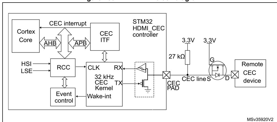
The CEC bus consists of a single bidirectional line that is used to transfer data in and out of the device. It is connected to a +3.3 V supply voltage via a 27 k \( \Omega \) pull-up resistor. The output stage of the device must have an open-drain or open-collector to allow a wired-AND connection.
The HDMI-CEC controller manages the CEC bidirectional line as an alternate function of a standard GPIO, assuming that it is configured as alternate function open drain. The 27 k \( \Omega \) pull-up must be added externally to the microcontroller.
To not interfere with the CEC bus when the application power is removed, it is mandatory to isolate the CEC pin from the bus in such conditions. This can be done by using a MOS transistor, as shown on Figure 283 .
Table 119. HDMI pin
| Name | Signal type | Remarks |
|---|---|---|
| CEC | Bidirectional | Two states: – 1 = high impedance – 0 = low impedance A 27 k \( \Omega \) resistor must be added externally. |
30.3.2 HDMI-CEC block diagram
Figure 283. HDMI-CEC block diagram
30.3.3 Message description
All transactions on the CEC line consist of an initiator and one or more followers. The initiator is responsible for sending the message structure and the data. The follower is the recipient of any data and is responsible for setting any acknowledgment bits.
A message is conveyed in a single frame that consists of a start bit followed by a header block and optionally an opcode and a variable number of operand blocks.
All these blocks are made of a 8-bit payload - most significant bit is transmitted first - followed by an end of message (EOM) bit and an acknowledge (ACK) bit.
The EOM bit is set in the last block of a message and kept reset in all others. In case a message contains additional blocks after an EOM is indicated, those additional blocks must be ignored. The EOM bit may be set in the header block to 'ping' other devices, to make sure they are active.
The acknowledge bit is always set to high impedance by the initiator so that it can be driven low either by the follower that has read its own address in the header, or by the follower that needs to reject a broadcast message.
The header consists of the source logical address field, and the destination logical address field. Note that the special address 0xF is used for broadcast messages.
Figure 284. Message structure
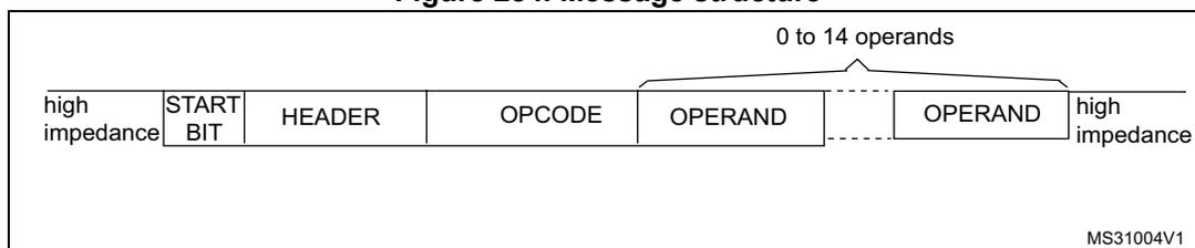
The diagram illustrates the structure of a CEC message. It begins with a 'high impedance' state, followed by a 'START BIT'. The message then contains a 'HEADER' block, an 'OPCODE' block, and a series of 'OPERAND' blocks. A bracket above the operand blocks indicates there can be '0 to 14 operands'. The message concludes with another 'high impedance' state. The identifier 'MS31004V1' is located in the bottom right corner.
Figure 285. Blocks
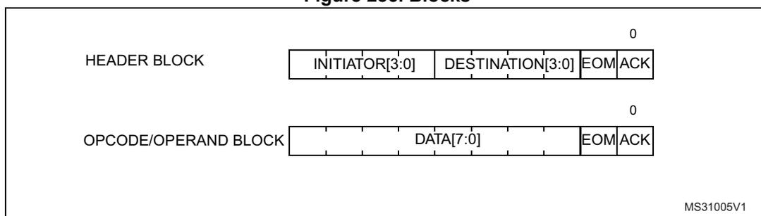
The diagram shows the internal bit structure of two types of blocks. The 'HEADER BLOCK' is an 8-bit byte containing 'INITIATOR[3:0]' (bits 7-4), 'DESTINATION[3:0]' (bits 3-0), 'EOM' (bit 1), and 'ACK' (bit 0). The 'OPCODE/OPERAND BLOCK' is also an 8-bit byte containing 'DATA[7:0]' (bits 7-0), 'EOM' (bit 1), and 'ACK' (bit 0). In both cases, the 'ACK' bit is set to '0' (high impedance). The identifier 'MS31005V1' is located in the bottom right corner.
30.3.4 Bit timing
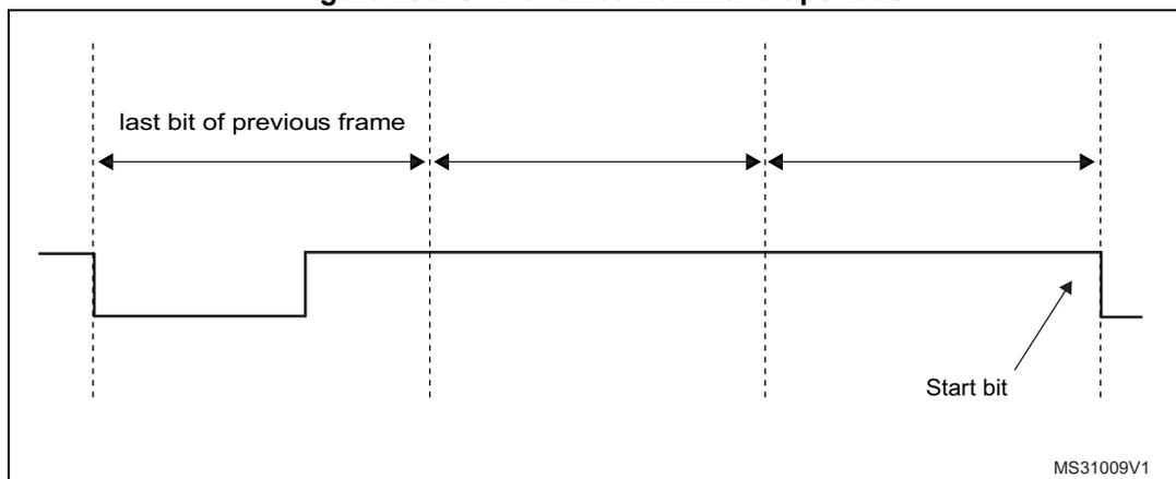
The format of the start bit is unique and identifies the start of a message. It must be validated by its low duration and its total duration.
All remaining data bits in the message, after the start bit, have consistent timing. The high-to-low transition at the end of the data bit is the start of the next data bit except for the final bit where the CEC line remains high.
Figure 286. Bit timings
START BIT
- high impedance: 4.5 ms +/-0.2 ms
- low impedance: 3.7 ms +/-0.2 ms
DATA BIT INITIATOR LOGICAL 0
- high impedance: 2.4 ms +/-0.35 ms
- low impedance: 1.5 ms +/-0.2 ms
DATA BIT INITIATOR LOGICAL 1
- high impedance: 2.4 ms +/-0.35 ms
- low impedance: 0.6 ms +/-0.2 ms
DATA BIT FOLLOWER LOGICAL 0
- high impedance: 2.4 ms +/-0.35 ms
- low impedance: 1.5 ms +/-0.2 ms
- initial low impedance: 0.35 ms max
MS31006V1
30.4 Arbitration
All devices transmitting - or retransmitting - a message onto the CEC line must ensure that it has been inactive for a number of bit periods. This signal-free time is defined as the time starting from the final bit of the previous frame and depends on the initiating device and the current status as shown in the figure below.
Figure 287. Signal free time
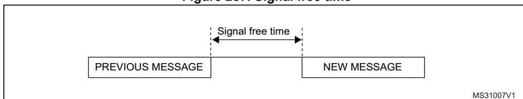
Signal free time
PREVIOUS MESSAGE
NEW MESSAGE
MS31007V1
Since only one initiator is allowed at any one time, an arbitration mechanism is provided to avoid conflict when more than one initiator begins transmitting at the same time.
CEC line arbitration starts with the leading edge of the start bit and continues until the end of the initiator address bits within the header block. During this period, the initiator must monitor the CEC line, if whilst driving the line to high impedance it reads it back to 0. Assuming then it has lost arbitration, it stops transmitting and becomes a follower.
Figure 288. Arbitration phase
![Figure 288: Arbitration phase diagram showing a sequence of fields: high impedance, START BIT, INITIATOR[3:0], DESTINATION[3:0], EOM, and ACK. The arbitration phase is indicated by a double-headed arrow spanning the START BIT and INITIATOR[3:0] fields. The diagram is labeled MS31008V1.](/RM0313-STM32F37/7d1249604ab4fc6b3ba852c3f558a399_img.jpg)
Figure 289 shows an example for a SFT of three nominal bit periods.
Figure 289. SFT of three nominal bit periods
A configurable time window is counted before starting the transmission.
In the SFT = 0 configuration, HDMI-CEC performs automatic SFT calculation ensuring compliance with the HDMI-CEC standard:
- • 2.5 data bit periods if the CEC is the last bus initiator with unsuccessful transmission
- • 4 data bit periods if the CEC is the new bus initiator
- • 6 data bit periods if the CEC is the last bus initiator with successful transmission
This is done to guarantee the maximum priority to a failed transmission and the lowest one to the last initiator that completed successfully its transmission.
Otherwise there is the possibility to configure the SFT bits to count a fixed timing value. Possible values are 0.5, 1.5, 2.5, 3.5, 4.5, 5.5, 6.5 data bit periods.
30.4.1 SFT option bit
In case of SFTOPT = 0 configuration, SFT starts being counted when the start-of-transmission command is set by software (TXSOM = 1).
In case of SFTOPT = 1, SFT starts automatically being counted by the HDMI-CEC device when a bus-idle or line error condition is detected. If the SFT timer is completed at the time TXSOM command is set then transmission starts immediately without latency. If the SFT timer is still running instead, the system waits until the timer elapses before transmission can start.
In case of SFTOPT = 1 a bus-event condition starting the SFT timer is detected in the following cases:
- • In case of a regular end of transmission/reception, when TXEND/RXEND bits are set at the minimum nominal data bit duration of the last bit in the message (ACK bit).
- • In case of a transmission error detection, SFT timer starts when the TXERR transmission error is detected (TXERR = 1).
- • In case of a missing acknowledge from the CEC follower, the SFT timer starts when the TXACKE bit is set, that is at the nominal sampling time of the ACK bit.
- • In case of a transmission underrun error, the SFT timer starts when the TXUDR bit is set at the end of the ACK bit.
- • In case of a receive error detection implying reception abort, the SFT timer starts at the same time the error is detected. If an error bit is generated, then SFT starts being counted at the end of the error bit.
- • In case of a wrong start bit or of any uncodified low impedance bus state from idle, the SFT timer is restarted as soon as the bus comes back to hi-impedance idleness.
30.5 Error handling
30.5.1 Bit error
If a data bit - excluding the start bit - is considered invalid, the follower is expected to notify such error by generating a low bit period on the CEC line of 1.4 to 1.6 times the nominal data bit period (3.6 ms nominally).
Figure 290. Error bit timing
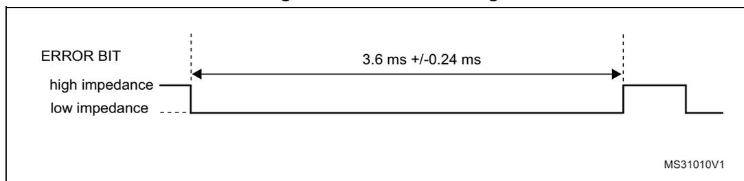
The diagram illustrates the timing for an error bit. It shows a signal line that transitions from a high impedance state to a low impedance state to create an 'ERROR BIT', and then returns to a high impedance state. The duration of the low impedance period is specified as 3.6 ms with a tolerance of +/- 0.24 ms. The diagram is labeled MS31010V1.
30.5.2 Message error
A message is considered lost and therefore may be retransmitted under the following conditions:
- • a message is not acknowledged in a directly addressed message
- • a message is negatively acknowledged in a broadcast message
- • a low impedance is detected on the CEC line while it is not expected (line error)
Three kinds of error flag can be detected when the CEC interface is receiving a data bit:
30.5.3 Bit rising error (BRE)
BRE (bit rising error) is set when a bit rising edge is detected outside the windows where it is expected (see Figure 291 ). BRE flag also generates a CEC interrupt if the BREIE = 1.
In the case of a BRE detection, the message reception can be stopped according to the BRESTP bit value and an error bit can be generated if BREGEN bit is set.
When BRE is detected in a broadcast message with BRESTP = 1 an error bit is generated even if BREGEN = 0 to enforce initiator's retry of the failed transmission. Error bit generation can be disabled by configuring BREGEN = 0, BRDNOGEN = 1.
30.5.4 Short bit period error (SBPE)
SBPE is set when a bit falling edge is detected earlier than expected (see Figure 291 ). SBPE flag also generates a CEC interrupt if the SBPEIE = 1.
An error bit is always generated on the line in case of a SBPE error detection. An error bit is not generated upon SBPE detection only when Listen mode is set (LSTN = 1) and the following conditions are met:
- • A directly addressed message is received containing SBPE
- • A broadcast message is received containing SBPE AND BRDNOGEN = 1
30.5.5 Long bit period error (LBPE)
LBPE is set when a bit falling edge is not detected in a valid window (see Figure 291 ). LBPE flag also generates a CEC interrupt if the LBPEIE = 1.
LBPE always stops the reception, an error bit is generated on the line when LBPEGEN bit is set.
When LBPE is detected in a broadcast message an error bit is generated even if LBPEGEN = 0 to enforce initiator's retry of the failed transmission. Error bit generation can be disabled by configuring LBPEGEN = 0, BRDNOGEN = 1.
Note: The BREGEN = 1, BRESTP = 0 configuration must be avoided.
Figure 291. Error handling
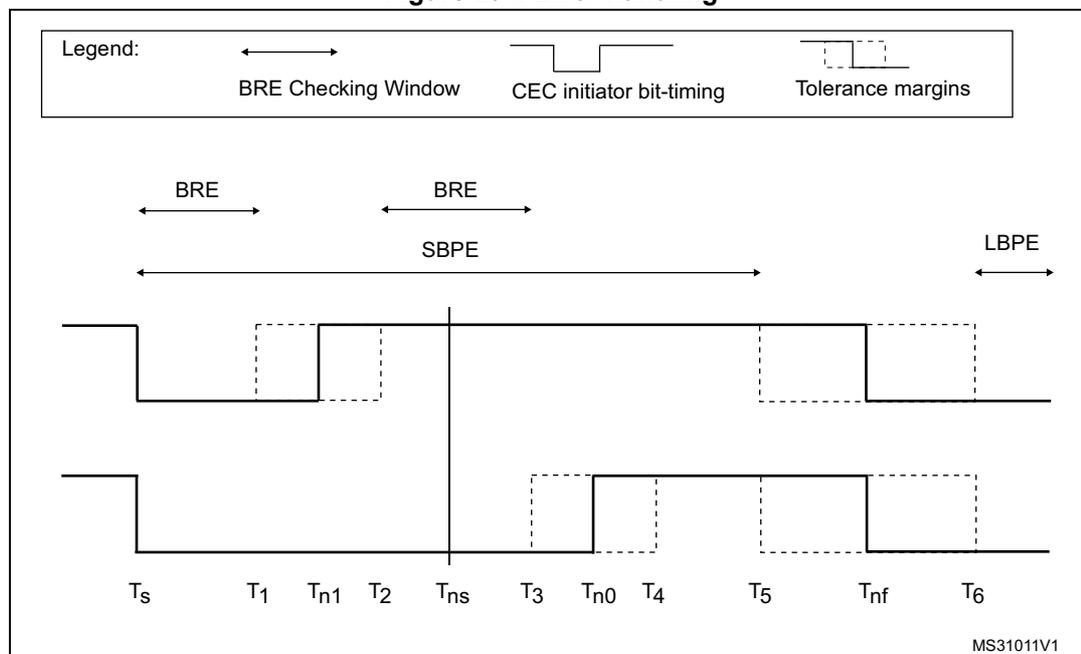
The figure is a timing diagram illustrating error handling on a CEC line. It shows two signal transitions. The top signal shows a BRE (Brown-out Reset Error) detected when the signal does not return to high within the BRE Checking Window. The bottom signal shows an SBPE (Short Bit Period Error) detected when the falling edge occurs earlier than expected, and an LBPE (Long Bit Period Error) detected when the falling edge is not detected within the expected window. The diagram includes a legend for BRE Checking Window, CEC initiator bit-timing, and Tolerance margins. Time markers Ts, T1, Tn1, T2, Tns, T3, Tn0, T4, T5, Tnf, and T6 are shown along the bottom. The diagram is labeled MS31011V1.
| Time | RXTOL | ms | Description |
|---|---|---|---|
| \( T_s \) | x | 0 | Bit start event. |
| \( T_1 \) | 1 | 0.3 | The earliest time for a low - high transition when indicating a logical 1. |
| 0 | 0.4 | ||
| \( T_{n1} \) | x | 0.6 | The nominal time for a low - high transition when indicating a logical 1. |
| \( T_2 \) | 0 | 0.8 | The latest time for a low - high transition when indicating a logical 1. |
| 1 | 0.9 | ||
| \( T_{ns} \) | x | 1.05 | Nominal sampling time. |
| \( T_3 \) | 1 | 1.2 | The earliest time a device is permitted return to a high impedance state (logical 0). |
| 0 | 1.3 | ||
| \( T_{n0} \) | x | 1.5 | The nominal time a device is permitted return to a high impedance state (logical 0). |
| \( T_4 \) | 0 | 1.7 | The latest time a device is permitted return to a high impedance state (logical 0). |
| 1 | 1.8 | ||
| \( T_5 \) | 1 | 1.85 | The earliest time for the start of a following bit. |
| 0 | 2.05 | ||
| \( T_{nf} \) | x | 2.4 | The nominal data bit period. |
| \( T_6 \) | 0 | 2.75 | The latest time for the start of a following bit. |
| 1 | 2.95 |
30.5.6 Transmission error detection (TXERR)
The CEC initiator sets the TXERR flag if detecting low impedance on the CEC line when it is transmitting high impedance and is not expecting a follower asserted bit. TXERR flag also generates a CEC interrupt if the TXERRIE = 1.
TXERR assertion stops the message transmission. Application is in charge to retry the failed transmission up to five times.
TXERR checks are performed differently depending on the different states of the CEC line and on the RX tolerance configuration.
Figure 292. TXERR detection
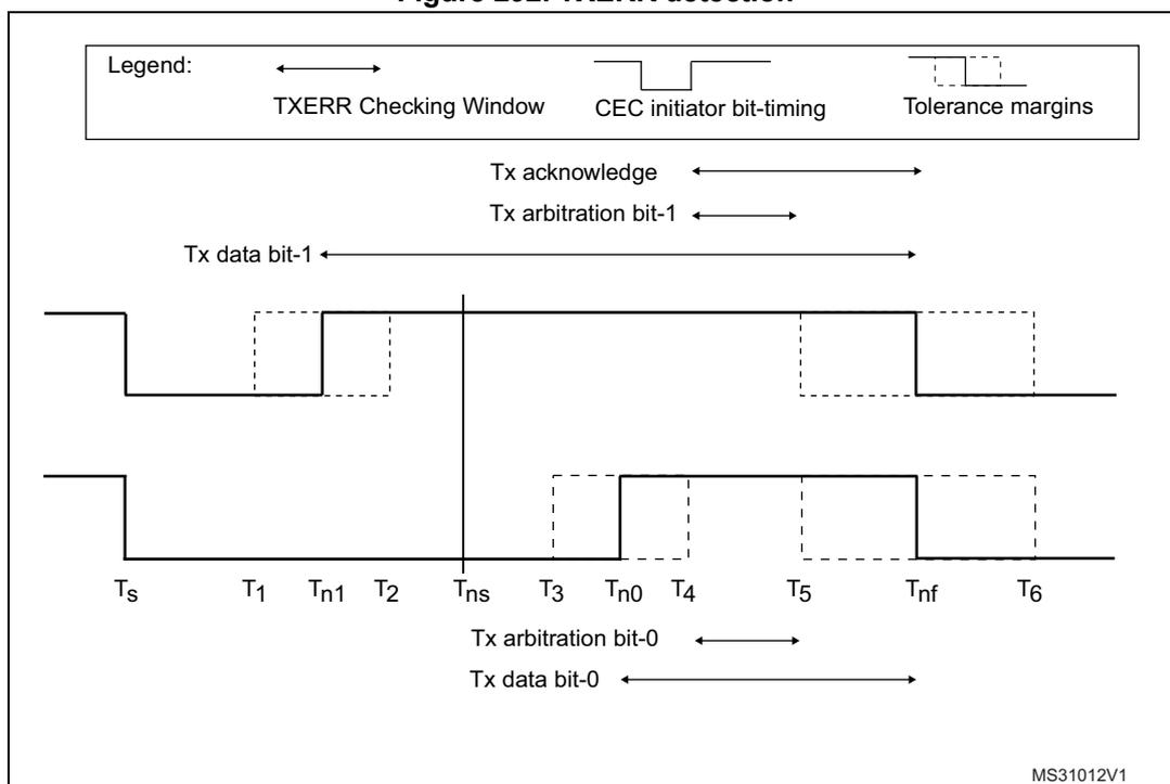
Legend:
- TXERR Checking Window (solid line with arrows)
- CEC initiator bit-timing (solid line with step)
- Tolerance margins (dashed line with step)
Signal levels and timing points:
- Tx data bit-1: High-to-low transition at \( T_s \) , low-to-high at \( T_1 \) , nominal at \( T_{n1} \) , latest at \( T_2 \) , sampling at \( T_{ns} \) .
- Tx arbitration bit-1: High-to-low transition at \( T_s \) , low-to-high at \( T_3 \) , nominal at \( T_{n0} \) , latest at \( T_4 \) , start of next bit at \( T_5 \) .
- Tx data bit-0: High-to-low transition at \( T_s \) , low-to-high at \( T_1 \) , nominal at \( T_{n1} \) , latest at \( T_2 \) , sampling at \( T_{ns} \) .
- Tx arbitration bit-0: High-to-low transition at \( T_s \) , low-to-high at \( T_3 \) , nominal at \( T_{n0} \) , latest at \( T_4 \) , start of next bit at \( T_5 \) .
MS31012V1
Table 121. TXERR timing parameters
| Time | RXTOL | ms | Description |
|---|---|---|---|
| \( T_s \) | x | 0 | Bit start event. |
| \( T_1 \) | 1 | 0.3 | The earliest time for a low - high transition when indicating a logical 1. |
| 0 | 0.4 | ||
| \( T_{n1} \) | x | 0.6 | The nominal time for a low - high transition when indicating a logical 1. |
| \( T_2 \) | 0 | 0.8 | The latest time for a low - high transition when indicating a logical 1. |
| 1 | 0.9 | ||
| \( T_{ns} \) | x | 1.05 | Nominal sampling time. |
| \( T_3 \) | 1 | 1.2 | The earliest time a device is permitted return to a high impedance state (logical 0). |
| 0 | 1.3 | ||
| \( T_{n0} \) | x | 1.5 | The nominal time a device is permitted return to a high impedance state (logical 0). |
| \( T_4 \) | 0 | 1.7 | The latest time a device is permitted return to a high impedance state (logical 0). |
| 1 | 1.8 | ||
| \( T_5 \) | 1 | 1.85 | The earliest time for the start of a following bit. |
| 0 | 2.05 | ||
| \( T_{nf} \) | x | 2.4 | The nominal data bit period. |
Table 121. TXERR timing parameters (continued)
| Time | RXTOL | ms | Description |
|---|---|---|---|
| T 6 | 0 | 2.75 | The latest time for the start of a following bit. |
| 1 | 2.95 |
30.6 HDMI-CEC interrupts
An interrupt can be produced:
- • during reception if a receive block transfer is finished or if a receive error occurs.
- • during transmission if a transmit block transfer is finished or if a transmit error occurs.
Table 122. HDMI-CEC interrupts
| Interrupt event | Event flag | Enable control bit |
|---|---|---|
| Rx-byte received | RXBR | RXBRIE |
| End of reception | RXEND | RXENDIE |
| Rx-overrun | RXOVR | RXOVRIE |
| Rxbit rising error | BRE | BREIE |
| Rx-short bit period error | SBPE | SBPEIE |
| Rx-long bit period error | LBPE | LBPEIE |
| Rx-missing acknowledge error | RXACKE | RXACKEIE |
| Arbitration lost | ARBLST | ARBLSTIE |
| Tx-byte request | TXBR | TXBRIE |
| End of transmission | TXEND | TXENDIE |
| Tx-buffer underrun | TXUDR | TXUDRIE |
| Tx-error | TXERR | TXERRIE |
| Tx-missing acknowledge error | TXACKE | TXACKEIE |
30.7 HDMI-CEC registers
Refer to Section 1.2 for a list of abbreviations used in register descriptions. The registers have to be accessed by words (32 bits).
30.7.1 CEC control register (CEC_CR)
Address offset: 0x00
Reset value: 0x0000 0000
| 31 | 30 | 29 | 28 | 27 | 26 | 25 | 24 | 23 | 22 | 21 | 20 | 19 | 18 | 17 | 16 |
|---|---|---|---|---|---|---|---|---|---|---|---|---|---|---|---|
| Res. | Res. | Res. | Res. | Res. | Res. | Res. | Res. | Res. | Res. | Res. | Res. | Res. | Res. | Res. | Res. |
| 15 | 14 | 13 | 12 | 11 | 10 | 9 | 8 | 7 | 6 | 5 | 4 | 3 | 2 | 1 | 0 |
| Res. | Res. | Res. | Res. | Res. | Res. | Res. | Res. | Res. | Res. | Res. | Res. | Res. | TXEOM rs | TXSOM rs | CECEN rw |
Bits 31:3 Reserved, must be kept at reset value.
Bit 2 TXEOM: Tx end of message
The TXEOM bit is set by software to command transmission of the last byte of a CEC message.
TXEOM is cleared by hardware at the same time and under the same conditions as for TXSOM.
0: TXDR data byte is transmitted with EOM = 0.
1: TXDR data byte is transmitted with EOM = 1.
Note: TXEOM must be set when CECEN = 1.
TXEOM must be set before writing transmission data to TXDR.
If TXEOM is set when TXSOM = 0, transmitted message consists of 1 byte (HEADER) only (PING message).
Bit 1 TXSOM: Tx start of message
TXSOM is set by software to command transmission of the first byte of a CEC message. If the CEC message consists of only one byte, TXEOM must be set before of TXSOM.
Start-bit is effectively started on the CEC line after SFT is counted. If TXSOM is set while a message reception is ongoing, transmission starts after the end of reception.
TXSOM is cleared by hardware after the last byte of the message is sent with a positive acknowledge (TXEND = 1), in case of transmission underrun (TXUDR = 1), negative acknowledge (TXACKE = 1), and transmission error (TXERR = 1). It is also cleared by CECEN = 0. It is not cleared and transmission is automatically retried in case of arbitration lost (ARBLST = 1).
TXSOM can be also used as a status bit informing application whether any transmission request is pending or under execution. The application can abort a transmission request at any time by clearing the CECEN bit.
0: No CEC transmission is on-going.
1: CEC transmission command
Note: TXSOM must be set when CECEN = 1.
TXSOM must be set when transmission data is available into TXDR.
HEADER first four bits containing own peripheral address are taken from TXDR[7:4], not from CEC_CFGR.OAR that is used only for reception.
Bit 0 CECEN : CEC enableThe CECEN bit is set and cleared by software. CECEN = 1 starts message reception and enables the TXSOM control. CECEN = 0 disables the CEC peripheral, clears all bits of CEC_CR register and aborts any on-going reception or transmission.
0: CEC peripheral is off.
1: CEC peripheral is on.
30.7.2 CEC configuration register (CEC_CFGR)
This register is used to configure the HDMI-CEC controller.
Address offset: 0x04
Reset value: 0x0000 0000
Caution: It is mandatory to write CEC_CFGR only when CECEN = 0.
| 31 | 30 | 29 | 28 | 27 | 26 | 25 | 24 | 23 | 22 | 21 | 20 | 19 | 18 | 17 | 16 |
|---|---|---|---|---|---|---|---|---|---|---|---|---|---|---|---|
| LSTN | OAR[14:0] | ||||||||||||||
| rw | rw | rw | rw | rw | rw | rw | rw | rw | rw | rw | rw | rw | rw | rw | rw |
| 15 | 14 | 13 | 12 | 11 | 10 | 9 | 8 | 7 | 6 | 5 | 4 | 3 | 2 | 1 | 0 |
| Res. | Res. | Res. | Res. | Res. | Res. | Res. | SFTOP | BRDN OGEN | LBPEG EN | BREGE N | BREST P | RXTOL | SFT[2:0] | ||
| rw | rw | rw | rw | rw | rw | rw | rw | rw | |||||||
LSTN bit is set and cleared by software.
0: CEC peripheral receives only message addressed to its own address (OAR). Messages addressed to different destination are ignored. Broadcast messages are always received.
1: CEC peripheral receives messages addressed to its own address (OAR) with positive acknowledge. Messages addressed to different destination are received, but without interfering with the CEC bus: no acknowledge sent.
Bits 30:16 OAR[14:0] : Own addresses configurationThe OAR bits are set by software to select which destination logical addresses has to be considered in receive mode. Each bit, when set, enables the CEC logical address identified by the given bit position.
At the end of HEADER reception, the received destination address is compared with the enabled addresses. In case of matching address, the incoming message is acknowledged and received. In case of non-matching address, the incoming message is received only in listen mode (LSTN = 1), but without acknowledge sent. Broadcast messages are always received.
Example:
OAR = 0b000 0000 0010 0001 means that CEC acknowledges addresses 0x0 and 0x5.
Consequently, each message directed to one of these addresses is received.
Bits 15:9 Reserved, must be kept at reset value.
Bit 8 SFTOP : SFT option bitThe SFTOPT bit is set and cleared by software.
0: SFT timer starts when TXSOM is set by software.
1: SFT timer starts automatically at the end of message transmission/reception.
Bit 7 BRDNOGEN : Avoid error-bit generation in broadcast
The BRDNOGEN bit is set and cleared by software.
0: BRE detection with BRESTP = 1 and BREGEN = 0 on a broadcast message generates an error-bit on the CEC line. LBPE detection with LBPEGEN = 0 on a broadcast message generates an error-bit on the CEC line.
1: Error-bit is not generated in the same condition as above. An error-bit is not generated even in case of an SBPE detection in a broadcast message if listen mode is set.
Bit 6 LBPEGEN : Generate error-bit on long bit period error
The LBPEGEN bit is set and cleared by software.
0: LBPE detection does not generate an error-bit on the CEC line.
1: LBPE detection generates an error-bit on the CEC line.
Note: If BRDNOGEN = 0, an error-bit is generated upon LBPE detection in broadcast even if LBPEGEN = 0.
Bit 5 BREGEN : Generate error-bit on bit rising error
The BREGEN bit is set and cleared by software.
0: BRE detection does not generate an error-bit on the CEC line.
1: BRE detection generates an error-bit on the CEC line (if BRESTP is set).
Note: If BRDNOGEN = 0, an error-bit is generated upon BRE detection with BRESTP = 1 in broadcast even if BREGEN = 0.
Bit 4 BRESTP : Rx-stop on bit rising error
The BRESTP bit is set and cleared by software.
0: BRE detection does not stop reception of the CEC message. Data bit is sampled at 1.05 ms.
1: BRE detection stops message reception.
Bit 3 RXTOL : Rx-tolerance
The RXTOL bit is set and cleared by software.
0: Standard tolerance margin:
- – Start-bit, +/- 200 µs rise, +/- 200 µs fall
- – Data-bit: +/- 200 µs rise, +/- 350 µs fall
1: Extended tolerance
- – Start-bit: +/- 400 µs rise, +/- 400 µs fall
- – Data-bit: +/- 300 µs rise, +/- 500 µs fall
Bits 2:0 SFT[2:0] : Signal free time
SFT bits are set by software. In the SFT = 0x0 configuration, the number of nominal data bit periods waited before transmission is ruled by hardware according to the transmission history. In all the other configurations the SFT number is determined by software.
0x0
- – 2.5 data-bit periods if CEC is the last bus initiator with unsuccessful transmission (ARBLST = 1, TXERR = 1, TXUDR = 1 or TXACKE = 1)
- – 4 data-bit periods if CEC is the new bus initiator
- – 6 data-bit periods if CEC is the last bus initiator with successful transmission (TXEOM = 1)
0x1: 0.5 nominal data bit periods
0x2: 1.5 nominal data bit periods
0x3: 2.5 nominal data bit periods
0x4: 3.5 nominal data bit periods
0x5: 4.5 nominal data bit periods
0x6: 5.5 nominal data bit periods
0x7: 6.5 nominal data bit periods
30.7.3 CEC Tx data register (CEC_TXDR)
Address offset: 0x8
Reset value: 0x0000 0000
| 31 | 30 | 29 | 28 | 27 | 26 | 25 | 24 | 23 | 22 | 21 | 20 | 19 | 18 | 17 | 16 |
|---|---|---|---|---|---|---|---|---|---|---|---|---|---|---|---|
| Res. | Res. | Res. | Res. | Res. | Res. | Res. | Res. | Res. | Res. | Res. | Res. | Res. | Res. | Res. | Res. |
| 15 | 14 | 13 | 12 | 11 | 10 | 9 | 8 | 7 | 6 | 5 | 4 | 3 | 2 | 1 | 0 |
| Res. | Res. | Res. | Res. | Res. | Res. | Res. | Res. | TXD[7:0] | |||||||
| w | w | w | w | w | w | w | w | ||||||||
Bits 31:8 Reserved, must be kept at reset value.
Bits 7:0 TXD[7:0] : Tx data
TXD is a write-only register containing the data byte to be transmitted.
30.7.4 CEC Rx data register (CEC_RXDR)
Address offset: 0xC
Reset value: 0x0000 0000
| 31 | 30 | 29 | 28 | 27 | 26 | 25 | 24 | 23 | 22 | 21 | 20 | 19 | 18 | 17 | 16 |
|---|---|---|---|---|---|---|---|---|---|---|---|---|---|---|---|
| Res. | Res. | Res. | Res. | Res. | Res. | Res. | Res. | Res. | Res. | Res. | Res. | Res. | Res. | Res. | Res. |
| 15 | 14 | 13 | 12 | 11 | 10 | 9 | 8 | 7 | 6 | 5 | 4 | 3 | 2 | 1 | 0 |
| Res. | Res. | Res. | Res. | Res. | Res. | Res. | Res. | RXD[7:0] | |||||||
| r | r | r | r | r | r | r | r | ||||||||
Bits 31:8 Reserved, must be kept at reset value.
Bits 7:0 RXD[7:0] : Rx data
RXD is read-only and contains the last data byte that has been received from the CEC line.
30.7.5 CEC interrupt and status register (CEC_ISR)
Address offset: 0x10
Reset value: 0x0000 0000
| 31 | 30 | 29 | 28 | 27 | 26 | 25 | 24 | 23 | 22 | 21 | 20 | 19 | 18 | 17 | 16 |
|---|---|---|---|---|---|---|---|---|---|---|---|---|---|---|---|
| Res. | Res. | Res. | Res. | Res. | Res. | Res. | Res. | Res. | Res. | Res. | Res. | Res. | Res. | Res. | Res. |
| 15 | 14 | 13 | 12 | 11 | 10 | 9 | 8 | 7 | 6 | 5 | 4 | 3 | 2 | 1 | 0 |
| Res. | Res. | Res. | TXACK E | TXERR | TXUDR | TXEND | TXBR | ARBLST | RXACK E | LBPE | SBPE | BRE | RXOVR | RXEND | RXBR |
| rc_w1 | rc_w1 | rc_w1 | rc_w1 | rc_w1 | rc_w1 | rc_w1 | rc_w1 | rc_w1 | rc_w1 | rc_w1 | rc_w1 | rc_w1 |
Bits 31:13 Reserved, must be kept at reset value.
Bit 12 TXACKE: Tx-missing acknowledge errorIn transmission mode, TXACKE is set by hardware to inform application that no acknowledge was received. In case of broadcast transmission, TXACKE informs application that a negative acknowledge was received. TXACKE aborts message transmission and clears TXSOM and TXEOM controls.
TXACKE is cleared by software write at 1.
Bit 11 TXERR: Tx-errorIn transmission mode, TXERR is set by hardware if the CEC initiator detects low impedance on the CEC line while it is released. TXERR aborts message transmission and clears TXSOM and TXEOM controls.
TXERR is cleared by software write at 1.
Bit 10 TXUDR: Tx-buffer underrunIn transmission mode, TXUDR is set by hardware if application was not in time to load TXDR before of next byte transmission. TXUDR aborts message transmission and clears TXSOM and TXEOM control bits.
TXUDR is cleared by software write at 1.
Bit 9 TXEND: End of transmissionTXEND is set by hardware to inform application that the last byte of the CEC message has been successfully transmitted. TXEND clears the TXSOM and TXEOM control bits.
TXEND is cleared by software write at 1.
Bit 8 TXBR: Tx-byte requestTXBR is set by hardware to inform application that the next transmission data has to be written to TXDR. TXBR is set when the 4th bit of currently transmitted byte is sent. Application must write the next byte to TXDR within six nominal data-bit periods before transmission underrun error occurs (TXUDR).
TXBR is cleared by software write at 1.
Bit 7 ARBLST: Arbitration lostARBLST is set by hardware to inform application that CEC device is switching to reception due to arbitration lost event following the TXSOM command. ARBLST can be due either to a contending CEC device starting earlier or starting at the same time but with higher HEADER priority. After ARBLST assertion TXSOM bit keeps pending for next transmission attempt.
ARBLST is cleared by software write at 1.
Bit 6 RXACKE: Rx-missing acknowledgeIn receive mode, RXACKE is set by hardware to inform application that no acknowledge was seen on the CEC line. RXACKE applies only for broadcast messages and in listen mode also for not directly addressed messages (destination address not enabled in OAR). RXACKE aborts message reception.
RXACKE is cleared by software write at 1.
Bit 5 LBPE: Rx-long bit period errorLBPE is set by hardware in case a data-bit waveform is detected with long bit period error. LBPE is set at the end of the maximum bit-extension tolerance allowed by RXTOL, in case falling edge is still longing. LBPE always stops reception of the CEC message. LBPE generates an error-bit on the CEC line if LBPEGEN = 1. In case of broadcast, error-bit is generated even in case of LBPEGEN = 0.
LBPE is cleared by software write at 1.
Bit 4 SBPE: Rx-short bit period errorSBPE is set by hardware in case a data-bit waveform is detected with short bit period error. SBPE is set at the time the anticipated falling edge occurs. SBPE generates an error-bit on the CEC line.
SBPE is cleared by software write at 1.
Bit 3 BRE : Rx-bit rising error
BRE is set by hardware in case a data-bit waveform is detected with bit rising error. BRE is set either at the time the misplaced rising edge occurs, or at the end of the maximum BRE tolerance allowed by RXTOL, in case rising edge is still longing. BRE stops message reception if BRESTOP = 1. BRE generates an error-bit on the CEC line if BREGEN = 1.
BRE is cleared by software write at 1.
Bit 2 RXOVR : Rx-overrun
RXOVR is set by hardware if RXBR is not yet cleared at the time a new byte is received on the CEC line and stored into RXD. RXOVR assertion stops message reception so that no acknowledge is sent. In case of broadcast, a negative acknowledge is sent.
RXOVR is cleared by software write at 1.
Bit 1 RXEND : End of reception
RXEND is set by hardware to inform application that the last byte of a CEC message is received from the CEC line and stored into the RXD buffer. RXEND is set at the same time of RXBR.
RXEND is cleared by software write at 1.
Bit 0 RXBR : Rx-byte received
The RXBR bit is set by hardware to inform application that a new byte has been received from the CEC line and stored into the RXD buffer.
RXBR is cleared by software write at 1.
30.7.6 CEC interrupt enable register (CEC_IER)
Address offset: 0x14
Reset value: 0x0000 0000
Caution: It is mandatory to write CEC_IER only when CECEN = 0.
| 31 | 30 | 29 | 28 | 27 | 26 | 25 | 24 | 23 | 22 | 21 | 20 | 19 | 18 | 17 | 16 |
|---|---|---|---|---|---|---|---|---|---|---|---|---|---|---|---|
| Res. | Res. | Res. | Res. | Res. | Res. | Res. | Res. | Res. | Res. | Res. | Res. | Res. | Res. | Res. | Res. |
| 15 | 14 | 13 | 12 | 11 | 10 | 9 | 8 | 7 | 6 | 5 | 4 | 3 | 2 | 1 | 0 |
| Res. | Res. | Res. | TXACKIE | TXERRIE | TXUDRIE | TXENDIE | TXBRIE | ARBLS TIE | RXACKIE | LBPEIE | SBPEIE | BREIE | RXOVR IE | RXENDIE | RXBRIE |
| rw | rw | rw | rw | rw | rw | rw | rw | rw | rw | rw | rw | rw |
Bits 31:13 Reserved, must be kept at reset value.
Bit 12 TXACKIE : Tx-missing acknowledge error interrupt enable
The TXACKIE bit is set and cleared by software.
0: TXACKIE interrupt disabled
1: TXACKIE interrupt enabled
Bit 11 TXERRIE : Tx-error interrupt enable
The TXERRIE bit is set and cleared by software.
0: TXERRIE interrupt disabled
1: TXERRIE interrupt enabled
Bit 10 TXUDRIE : Tx-underrun interrupt enable
The TXUDRIE bit is set and cleared by software.
0: TXUDRIE interrupt disabled
1: TXUDRIE interrupt enabled
- Bit 9
TXENDIE
: Tx-end of message interrupt enable
The TXENDIE bit is set and cleared by software.
0: TXEND interrupt disabled
1: TXEND interrupt enabled - Bit 8
TXBRIE
: Tx-byte request interrupt enable
The TXBRIE bit is set and cleared by software.
0: TXBR interrupt disabled
1: TXBR interrupt enabled - Bit 7
ARBLSTIE
: Arbitration lost interrupt enable
The ARBLSTIE bit is set and cleared by software.
0: ARBLST interrupt disabled
1: ARBLST interrupt enabled - Bit 6
RXACKIE
: Rx-missing acknowledge error interrupt enable
The RXACKIE bit is set and cleared by software.
0: RXACKE interrupt disabled
1: RXACKE interrupt enabled - Bit 5
LBPEIE
: Long bit period error interrupt enable
The LBPEIE bit is set and cleared by software.
0: LBPE interrupt disabled
1: LBPE interrupt enabled - Bit 4
SBPEIE
: Short bit period error interrupt enable
The SBPEIE bit is set and cleared by software.
0: SBPE interrupt disabled
1: SBPE interrupt enabled - Bit 3
BREIE
: Bit rising error interrupt enable
The BREIE bit is set and cleared by software.
0: BRE interrupt disabled
1: BRE interrupt enabled - Bit 2
RXOVRIE
: Rx-buffer overrun interrupt enable
The RXOVRIE bit is set and cleared by software.
0: RXOVR interrupt disabled
1: RXOVR interrupt enabled - Bit 1
RXENDIE
: End of reception interrupt enable
The RXENDIE bit is set and cleared by software.
0: RXEND interrupt disabled
1: RXEND interrupt enabled - Bit 0
RXBRIE
: Rx-byte received interrupt enable
The RXBRIE bit is set and cleared by software.
0: RXBR interrupt disabled
1: RXBR interrupt enabled
30.7.7 HDMI-CEC register map
Table 123. HDMI-CEC register map and reset values
| Offset | Register name | 31 | 30 | 29 | 28 | 27 | 26 | 25 | 24 | 23 | 22 | 21 | 20 | 19 | 18 | 17 | 16 | 15 | 14 | 13 | 12 | 11 | 10 | 9 | 8 | 7 | 6 | 5 | 4 | 3 | 2 | 1 | 0 |
|---|---|---|---|---|---|---|---|---|---|---|---|---|---|---|---|---|---|---|---|---|---|---|---|---|---|---|---|---|---|---|---|---|---|
| 0x00 | CEC_CR | Res. | Res. | Res. | Res. | Res. | Res. | Res. | Res. | Res. | Res. | Res. | Res. | Res. | Res. | Res. | Res. | Res. | Res. | Res. | Res. | Res. | Res. | Res. | Res. | Res. | Res. | Res. | Res. | Res. | TXEOM | TXSOM | CECEN |
| Reset value | 0 | 0 | 0 | ||||||||||||||||||||||||||||||
| 0x04 | CEC_CFGR | LSTN | OAR[14:0] | Res. | Res. | Res. | Res. | Res. | Res. | Res. | SFTOPT | BRDNOGEN | LBPEGEN | BREGEN | BRESTP | RXTOL | SFT[2:0] | ||||||||||||||||
| Reset value | 0 | 0 | 0 | 0 | 0 | 0 | 0 | 0 | 0 | 0 | 0 | 0 | 0 | 0 | 0 | 0 | 0 | 0 | 0 | 0 | 0 | 0 | 0 | 0 | 0 | ||||||||
| 0x08 | CEC_TXDR | Res. | Res. | Res. | Res. | Res. | Res. | Res. | Res. | Res. | Res. | Res. | Res. | Res. | Res. | Res. | Res. | Res. | Res. | Res. | Res. | Res. | Res. | Res. | Res. | TXD[7:0] | |||||||
| Reset value | 0 | 0 | 0 | 0 | 0 | 0 | 0 | 0 | |||||||||||||||||||||||||
| 0x0C | CEC_RXDR | Res. | Res. | Res. | Res. | Res. | Res. | Res. | Res. | Res. | Res. | Res. | Res. | Res. | Res. | Res. | Res. | Res. | Res. | Res. | Res. | Res. | Res. | Res. | Res. | RXD[7:0] | |||||||
| Reset value | 0 | 0 | 0 | 0 | 0 | 0 | 0 | 0 | |||||||||||||||||||||||||
| 0x10 | CEC_ISR | Res. | Res. | Res. | Res. | Res. | Res. | Res. | Res. | Res. | Res. | Res. | Res. | Res. | Res. | Res. | Res. | Res. | Res. | Res. | TXACKE | TXERR | TXUDR | TXEND | TXBR | ARBLST | RXACKE | LBPE | SBPE | BRE | RXOVR | RXEND | RXBR |
| Reset value | 0 | 0 | 0 | 0 | 0 | 0 | 0 | 0 | 0 | 0 | 0 | 0 | 0 | ||||||||||||||||||||
| 0x14 | CEC_IER | Res. | Res. | Res. | Res. | Res. | Res. | Res. | Res. | Res. | Res. | Res. | Res. | Res. | Res. | Res. | Res. | Res. | Res. | Res. | TXACKIE | TXERRIE | TXUDRIE | TXENDIE | TXBRIE | ARBLSTIE | RXACKIE | LBPEIE | SBPEIE | BREIE | RXOVRIE | RXENDIE | RXBRIE |
| Reset value | 0 | 0 | 0 | 0 | 0 | 0 | 0 | 0 | 0 | 0 | 0 | 0 | 0 | ||||||||||||||||||||