13. Sigma-delta analog-to-digital converter (SDADC)
13.1 Introduction
The SDADC module is a high-performance and low-power sigma-delta analog-to-digital converter, featuring 16-bit resolution and 9 differential analog channels with selectable gains.
The conversion speed is up to 16.6 ksps (kilo-samples per second) for each SDADC when converting multiple channels and up to 50 ksps per SDADC if only one channel conversion is used. There are two conversion modes: single conversion mode and continuous mode, capable of automatically scanning any number of channels. The data can be automatically stored in a system RAM buffer, reducing the software overhead.
A flexible timer triggering system can be used to control the start of conversion of the three SDADCs. This timing control is capable of triggering simultaneous conversions or inserting a programmable delay between the SDADCs.
Reference voltage for SDADC can be selected from external reference pins, internal 1.2/1.8V reference or SDADC analog power supply.
Four power modes are supported: Normal, Slow, Standby and Power down. In Standby mode, references stay powered on to reduce the startup time.
13.2 SDADC main features
- • 16-bit sigma-delta architecture
- • 5 differential input pairs, or 9 single-ended inputs, or a combination
- • High-performance data throughput:
- – 16.6 ksps input sampling rate when multiplexing between different channels
- – 50 ksps input sampling rate for single-channel operation
- • Self-calibration (offset)
- • 7 gain settings from 0.5x to 32x (analog gains: 0.5 - 8, digital gains: 16 - 32)
- • Full-scale single-ended conversion mode referenced to ground in addition to differential mode
- • Each channel can choose between 3 user-defined configurations, where each configuration specifies:
- – Analog gain at the input of the channel
- – Conversion mode: differential vs. full-scale single-ended referenced to ground
- – Calibration offset
- • Selectable reference voltage which determines the input signal range and digital end-of-scale:
- – Internal VDDSDx: \( V_{REFSD} = \text{analog supply, 2.4 V-3.6 V (2.2 V-3.6 V in Slow mode)} \)
- – Internal bandgap: \( V_{REFSD} = 1.2 \text{ V} \)
- – Internal bandgap (1.5x amplified): \( V_{REFSD} = 1.8 \text{ V} \)
- – External reference on VREFSD+ pin: \( V_{REFSD+} = 1.1 \text{ V} \) to analog supply
- • Continuous conversion
- • Start-of-conversion synchronization with
- – Software trigger
- – Internal timers
- – External events
- – start-of-conversion of another (first) SDADC
- • “Regular” conversions can be requested at any time or even in continuous mode without having any impact on the timing of “injected” conversions
- • Two's-complement output format
- • DMA may be used to read the conversion data
- • End of conversion, overrun, and end of calibration interrupts
- • 3 low-power modes (refer to the datasheet for the current consumption values):
- – Slow mode where the device operates from a reduced clock frequency
- – Standby mode
- – Power down mode
- • All three SDADCs can share up to 23 input pins which may be configured in any combination of single-ended (up to 21) or differential inputs (up to 11).
13.3 SDADC pins
Table 36. ADC pins
| Name | Signal Type | Remarks |
|---|---|---|
| VREFSD+ | Input or In/Out, positive analog reference | When the external reference is selected (REFV=00), this pin must be driven externally to a voltage between 1.1 V and VDDSDx. When an internal reference is selected (REFV is 01, 10, or 11), this pin must have an external capacitance connected to VREFSD-. |
| VREFSD- | Input, negative analog reference | This pin, when present, must be driven to the same voltage level as VSSSD. |
| VDDSDx | Input, analog supply | Analog power supply. Must be greater than 2.4 V (or 2.2 V in Slow mode) and less than 3.6 V. |
| VSSSD | Input, analog supply ground | Analog ground power supply. |
| SDADCx_AIN[8:0]P | Analog input | Positive differential analog inputs for the 9 channels. |
| SDADCx_AIN[8:0]M | Analog input | Negative differential analog inputs for the 9 channels. |
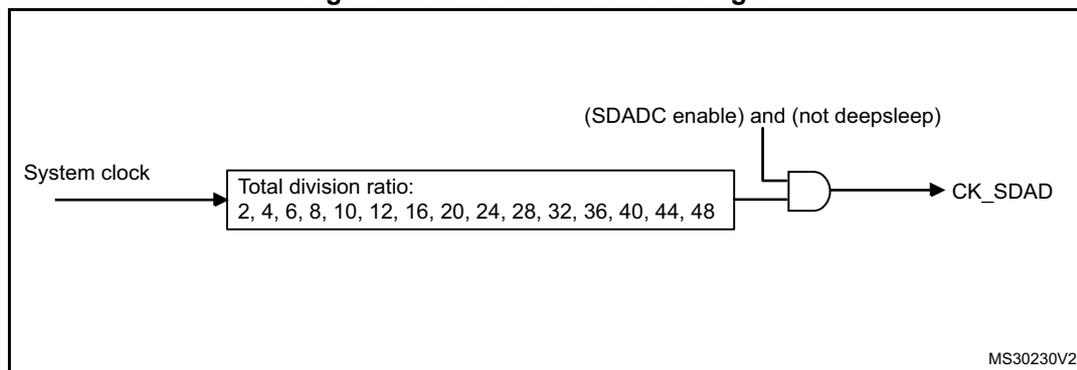
13.4 SDADC clock
The clock source for SDADC is derived from the system clock. This clock is divided by a selectable divider with 50% duty cycle.
Any of the following division ratios can be selected:
2, 4, 6, 8, 10, 12, 14, 16, 20, 24, 28, 32, 36, 40, 44, 48.
The SDADC clock is automatically stopped in deepsleep mode.
The maximum operating frequency of the SDADC is 6 MHz. Its minimum operating frequency is 500 kHz.
A detailed diagram of SDADC clock is given in Section 7.2.9: SDADC clock on page 109
Figure 35. SDADC clock block diagram
13.5 SDADC functional description
Figure 36. Single SDADC block diagram
![Figure 36. Single SDADC block diagram. The diagram shows the internal architecture of the SDADC. On the left, multiple differential input pairs (SD_ADCx_AIN0P/0M, SD_ADCx_AIN1P/1M, ..., SD_ADCx_AIN8P/8M) are connected to a multiplexer. The output of the multiplexer is connected to a gain block (Gain 0.5...32). The gain block output is connected to a sigma-delta modulator (ΣΔ). The modulator has inputs for reference voltage (REFV), slow clock (SLOWCK), and a start signal. The output of the modulator is connected to a digital filter. The digital filter has two outputs: JDATA[15:0] and RDATA[15:0]. The digital filter is controlled by a configuration block (configuration) which includes a configuration selector and configuration registers (CONFCH0[1:0], CONFCH1[1:0], ..., CONFCH8[1:0]). The configuration block is also connected to a channel selector (Injected channels JCHG[8:0], Regular channel RCH[3:0]). The SDADC clock (ck_sdad) is derived from the RCC (6 MHz or 1.5 MHz, min 500 kHz). The VDDSDx supply is connected to the modulator. The SDADC interrupt is generated by an AND gate with inputs from various flags (JEOCF, JEOCIE, JOVRF, JOVRIE, REOCF, REOCIE, ROVRF, ROVRIE, EOCALF, EOCALIE). The start signal for the modulator is generated by a logic block (JSTART) which includes inputs for RSWSTART, RSYNC, RSWSTART1, JSYNC, JSTART1, JSWSTART, JEXTEN, JEXTSEL, and TIMx/TIMy. A note indicates that the logic for JSTART is implemented only in SDADC2 and SDADC3. The diagram is labeled MS30934V2.](/RM0313-STM32F37/7d675e1c380dccba3f69e2de4e72562c_img.jpg)
13.5.1 SDADC on-off control
The SDADC is enabled by setting the ADON bit in the SDADC_CR2 register. After the SDADC is powered on, it needs 100 \( \mu\text{s} \) to stabilize before it can start a conversion or launch calibration (unless PDI=1, see next section). An action requested in the meantime will be automatically started as soon as stabilization is complete. The end of stabilization is signalled by bit STABIP in the SDADC_ISR register.
Clearing ADON stops any conversion which may be in progress and puts the SDADC in power down mode.
13.5.2 Power down and Standby low-power modes
In order to reduce consumption, the SDADC can be automatically put into either Standby mode or power down mode when it is idle. "Idle" is defined as when RCIP=0, JCIP=0, and CALIBIP=0.
Setting PDI in the SDADC_CR1 register causes the SDADC to enter power down mode when idle, where it consumes about 10 µA instead of up to 1.2 mA (see datasheet for exact values). Whenever exiting power down mode, a period of 100 µs is needed for stabilization. During stabilization, a conversion may be requested, but it will not start until stabilization is complete (STABIP=0).
Similarly, setting SBI in the SDADC_CR1 register puts the SDADC in Standby mode when idle, where it consumes a maximum of about 200 µA. Whenever exiting Standby mode conversions, a period of 50 µs is required for stabilization.
While the SDADC is stabilizing, the stabilization in progress status bit, STABIP, in SDADC_ISR is set to '1'.
When enforcing the stabilization times, the SDADC measures these durations assuming that the prescaler outputs a clock at 6 MHz. This means that the 100 µs period after power on is defined as 600 SDADC clock cycles (or 150 if SLOWCK=1, where the SDADC frequency should be 1.5 MHz), and the 50 µs period after exiting Standby mode is defined as 300 SDADC clock cycles (or 75 if SLOWCK=1).
When SBI=1, if a conversion or calibration is requested within the first 50 µs after ADON is activated, a stabilization period of 100 µs (rather than 50 µs) is observed starting from the moment that the conversion or calibration is requested.
13.5.3 SDADC clock
The SDADC clock, which is used to drive the analog logic, is generated by the RCC block. When not in Slow mode, its prescaler should be configured so that the SDADC can run at its maximum frequency of 6 MHz. The minimum operating frequency of the SDADC is 500 kHz.
Slow mode
Setting the SLOWCK bit in the SDADC_CR1 register puts the SDADC in Slow mode. When SLOWCK=1, the analog consumes less and is able to operate down to a voltage of 2.2 V, but the frequency of the SDADC clock must be reduced to 1.5 MHz. The minimum frequency is still 500 kHz in Slow mode.
13.5.4 Channel selection
There are 9 multiplexed channels which can be selected for conversion using the injected channel group and using the regular channel.
The injected channel group is a selection of any or all of the 9 channels. JCHG[8:0] in the SDADC_JCHGR register selects the channels of the injected group, where JCHG[i]=1 means that channel i is selected.
Injected conversions are always executed in scan mode, which means that each of the selected channels are converted in series. The lowest selected channel is converted first, followed immediately by the next higher selected channel until all the channels selected by JCHG[8:0] have been converted.
Injected conversions can be launched by software or by a trigger. They are never interrupted by regular conversions.
The regular channel is a selection of just one of the 9 channels. RCH[3:0] in the SDADC_CR2 register indicates the selected channel.
Regular conversions can be launched only by software (not by a trigger). A sequence of continuous regular conversions is temporarily interrupted when a injected conversion is requested.
13.5.5 Differential and single-ended modes
Each SDADC channel has 2 differential inputs (positive and negative: SDADCx_AIN[n]P, SDADCx_AIN[n]M). Configuring of those inputs to pins connection can be obtained several measurement modes.
Differential mode: Simple mode where both - positive and negative inputs - are connected to external pins. The output signal is positive or negative depending on the connected signal polarity. The corresponding SE[1:0] bits must be set to “00” (see Section 13.5.6: Configuring the analog inputs ) to select this mode.
In additional to this differential mode, conversions may be performed in one of two single-ended modes. When in single-ended mode, the negative input is set to VREFSD- pin internally, leaving the corresponding pin for the negative input (SDADCx_AIN[n]M) free to be used for other purposes. The signal to be measured is applied to the positive input.
Single-ended offset mode: The corresponding SE[1:0] bits must be set to “01” (see Section 13.5.6: Configuring the analog inputs ) to select this mode. The output signal is always positive, thus excluding the negative half of the dynamic range. In this mode, the signal to noise ratio (SNR) is degraded by 6 dB.
Single-ended zero reference mode: The corresponding SE[1:0] bits must be set to “11” (see Section 13.5.6: Configuring the analog inputs ) to select this mode. This mode injects an offset of half scale to the SDADC thus maintaining the full positive/negative dynamic range like in differential mode. In this mode, the offset is dependent on gain variations.
The correct application design of the PCB is important for a good SDADC analog performance. The STM32F37x device has several ground (and voltage supply) signals, which must be designed according Section 6.1.2: Correct grounding for analog applications .
Examples of possible modes Figure 37. Switch configuration in single-ended mode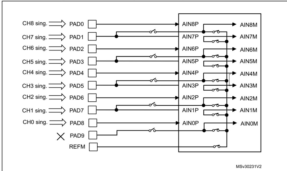
The diagram illustrates the internal switch configuration for single-ended mode. On the left, external connections are labeled: CH8 sing. to PAD0, CH7 sing. to PAD1, CH6 sing. to PAD2, CH5 sing. to PAD3, CH4 sing. to PAD4, CH3 sing. to PAD5, CH2 sing. to PAD6, CH1 sing. to PAD7, CH0 sing. to PAD8, PAD9 (marked with an X), and REF M. Each pad connects to an internal node: PAD0 to AIN8P, PAD1 to AIN7P, PAD2 to AIN6P, PAD3 to AIN5P, PAD4 to AIN4P, PAD5 to AIN3P, PAD6 to AIN2P, PAD7 to AIN1P, PAD8 to AIN0P, PAD9 to a common node, and REF M to the same common node. Each positive node (AIN0P to AIN8P) is connected via a switch to its corresponding negative node (AIN0M to AIN8M). All switches on the left (between pads and positive nodes) are shown as open. All switches on the right (between positive nodes and negative nodes) are shown as closed. The common node for PAD9 and REF M is also connected to all negative nodes (AIN0M to AIN8M) via a single switch. The diagram is labeled MSV30231V2 in the bottom right corner.
- • All analog switches on the left are open.
- • All analog switches on the right are closed.
- • CH8 to CH0 are used in single-ended mode.
- • REF M is used (connected internally to VREFSD- pin).
- • PAD 9 is not used.
Figure 38. Switch configuration in differential mode
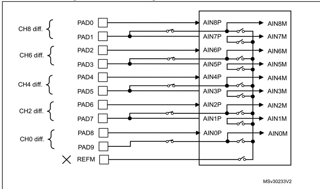
The diagram illustrates the internal switch configuration of an SDADC in differential mode. On the left, external pads are labeled PAD0 through PAD9 and REFM. Brackets on the far left group these into differential channels: CH8 diff. (PAD0, PAD1), CH6 diff. (PAD2, PAD3), CH4 diff. (PAD4, PAD5), CH2 diff. (PAD6, PAD7), and CH0 diff. (PAD8, PAD9). The REFM pad is marked with an 'X', indicating it is not used. On the right, internal nodes are labeled AIN0P through AIN8P and AIN0M through AIN8M. Switches connect each pad to its corresponding positive internal node (e.g., PAD0 to AIN8P). Additional switches connect these positive nodes to their corresponding negative internal nodes (e.g., AIN8P to AIN8M). The diagram shows that for the active channels (CH8, CH6, CH4, CH2, CH0), the switches on the left are closed and the switches on the right are open. For the unused channels (CH7, CH5, CH3, CH1) and REFM, the switches are open.
MSV30233V2
- • All analog switches on the left are closed.
- • All analog switches on the right are open.
- • CH8, CH6, CH4, CH2, and CH0 are in differential mode.
- • CH7, CH5, CH3 and CH1 are not used.
- • REFM is not used.
Figure 39. Switch configuration in mixed mode (example 1)
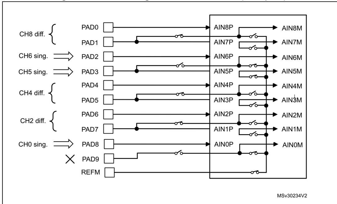
The diagram illustrates the internal switch configuration for the SDADC in mixed mode. The pads are arranged vertically on the left: PAD0 through PAD9, and REFM. On the right, a block represents the SDADC with internal pins AIN8P/M down to AIN0P/M. Connections are as follows:
- CH8 diff. : PAD0 connects to AIN8P. PAD1 connects to AIN7P. Switches allow routing to AIN8M and AIN7M.
- CH6 sing. : PAD2 connects to AIN6P.
- CH5 sing. : PAD3 connects to AIN5P via a switch.
- CH4 diff. : PAD4 connects to AIN4P. PAD5 connects to AIN3P. Switches allow routing to AIN4M and AIN3M.
- CH2 diff. : PAD6 connects to AIN2P. PAD7 connects to AIN1P. Switches allow routing to AIN2M and AIN1M.
- CH0 sing. : PAD8 connects to AIN0P.
- PAD9 : Marked with an 'X', indicating it is not used.
- REFM : Connects to a common internal reference line that can be switched to the negative inputs (AINxM) of the channels.
MSV30234V2
- • CH8, CH4 and CH2 are used as differential.
- • CH6, CH5 and CH0 are used in single-ended mode.
- • REFM is used (connected internally to VREFSD- pin).
- • PAD 9 is not used.
Figure 40. Switch configuration in mixed mode (example 2)
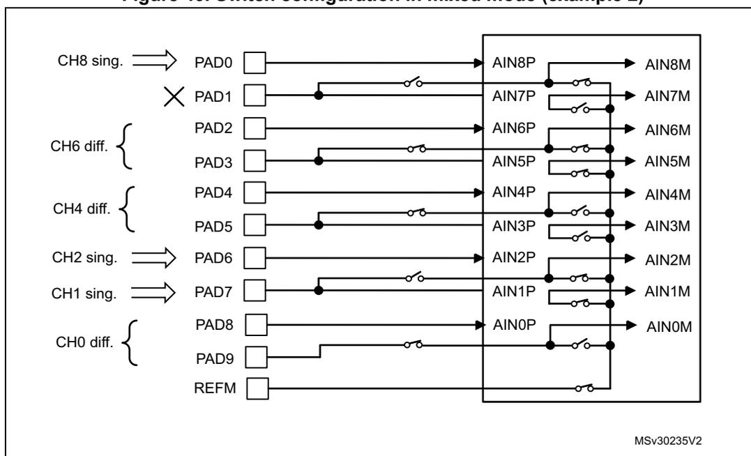
- • CH6, CH4 and CH0 are used as differential.
- • CH8, CH2 and CH1 are used in single-ended mode.
- • REF M is used (connected internally to VREFSD- pin).
- • PAD 1 is not used.
13.5.6 Configuring the analog inputs
The following parameters must be configured for the analog inputs:
- • Gain. There are 5 analog gain settings (1/2x, 1x, 2x, 4x, 8x) and 2 digital gain settings (16x, 32x).
- • Single-ended modes (SE) (see Section 13.5.5: Differential and single-ended modes ).
- • Common mode. The common mode setting (VSSSD, VDDSDx, or VDDSDx/2) is used only in the determination of the offset during the calibration sequence.
- • Offset. The 12-bit offset is applied to the conversion results. This value varies from part to part and also depends on the common mode, on the SE setting, and on the gain if SE=11. This value can be determined automatically during the calibration sequence or it can be written by software.
Three distinct configurations can be specified using the SDADC_CONF0R, SDADC_CONF1R, and SDADC_CONF2R registers. Each SDADC_CONFxR register contains the fields GAINx[2:0], COMMONx[1:0], SE[1:0], and OFFSETx[11:0].
Each individual input can select one of the three configurations, by way of the SDADC_CONFCHR1 and SDADC_CONFCHR2 registers.
13.5.7 Launching calibration and determining the offset values
Calibration can be used to determine the offset values of the configurations defined in each of the three SDADC_CONFxR registers. OFFSETx[11:0] is determined based on GAINx[2:0], COMMONx[1:0], and SEx[1:0] (where x is 0, 1, or 2).
During the offset calibration positive and negative SDADC inputs are shorted internally and connected to common voltage given by COMMONx[1:0] setting. GAINx[2:0] is applied and then is performed a conversion which determines the OFFSETx[11:0] value (12-bit signed value).
The calibration sequence consists of the following steps:
- • The SDADC_CONFxR registers must be written. If only 1 distinct configuration is used, then it must be defined in the SDADC_CONF0R register. If only 2 distinct configurations are used, then they must be defined in the SDADC_CONF0R and SDADC_CONF1R registers.
- • The SDADC_CR2 register is written:
- – “00” written to CALIBCNT[1:0] if only OFFSET0 is to be determined, “01” for both OFFSET0 and OFFSET1, or “10” to determine all three offset values,
- – ‘1’ must be written to STARTCALIB to launch calibration.
- • The calibration sequence then executes, taking 30720 ADC cycles (5.12 ms at 6 MHz) for each offset calculation. Thus, all three offsets are calculated, the entire sequence lasts 15.36 ms at 6 MHz.
- • The offset values are automatically stored in the corresponding OFFSETx[11:0] fields.
13.5.8 Launching conversions
Injected conversions can be launched using the following methods:
- • Software: writing ‘1’ to the JSWSTART bit in the SDADC_CR2 register.
- • Trigger: the JEXTSEL[2:0] bits select the trigger signal while the JEXTEN bit activates the trigger and selects the active edge at the same time.
- • Synchronous with SDADC1: for SDADC2 or SDADC3, an injected conversion is automatically launched when an action in SDADC1 causes its own injected conversion sequence to start. Each injected conversion in SDADC2 or SDADC3 is always executed according its local configuration settings (JDS, JCONT, JCHG, etc.).
Each time an injected conversion is launched, all of the selected channels in the injected group are converted sequentially, starting with the lowest selected channel.
Only one injected conversion can be pending or ongoing at a given time. Thus, any request to launch an injected conversion is ignored if another request for an injected conversion has already been issued but not yet completed.
Regular conversions can be launched using the following methods:
- • Software: by writing ‘1’ to RSWSTART in the SDADC_CR2 register.
- • Synchronous with SDADC1: for SDADC2 or SDADC3, a regular conversion is automatically launched when an action in SDADC1 causes its own regular conversion sequence to start. Each regular conversion in SDADC2 or SDADC3 is always executed according its local configuration settings (RCONT, RCH, etc.).
Only one regular conversion can be pending or ongoing at a given time. Thus, any request to launch a regular conversion is ignored if another request for a regular conversion has already been issued but not yet completed.
13.5.9 Continuous and fast continuous modes
Setting the JCONT bit in the SDADC_CR2 register causes injected conversions launched by software to execute in continuous mode. If software writes ‘1’ to the JCONT bit at the
same time as it writes '1' to the JSWSTART bit, the same scan sequence is performed repeatedly, always starting over at the lowest selected channel after the highest selected channel is finished.
Similarly, setting the RCONT bit causes regular conversions to execute in continuous mode. RCONT=1 means that the channel selected by the RCH[3:0] bits is converted repeatedly after '1' is written to the RSWSTART bit.
The sequence of injected conversions executing in continuous mode can be stopped by writing '0' to the JCONT bit. After clearing the JCONT bit, only the on-going conversion will be completed; the scan sequence is interrupted, and thus the final conversion will not be the last (highest) selected channel unless it was the one being converted when the JCONT bit was cleared.
Similarly, writing '0' to the RCONT bit stops continuous regular conversions, allowing only the currently executing conversion to complete.
If just a single channel is selected in continuous mode (either by executing a regular conversion or by executing a injected conversion with only one channel selected), the sampling rate can be increased three fold by setting the FAST bit in the SDADC_CR2 register. The conversion of each channel normally requires 360 SDADC clock cycles (60 µs at 6 MHz). In fast continuous mode (FAST=1), the first conversion takes still 360 SDADC clocks, but then each subsequent conversion finishes in 120 SDADC clocks.
13.5.10 Request precedence
In summary, the calibration sequence has the highest precedence, followed by injected conversions, while regular conversions have the lowest priority. However, an individual conversion which is already in progress is never interrupted by the request for another action. Also, a request is ignored if a like action is already pending or in progress. Finally, no action can start before stabilization has finished. The following text gives examples and more details.
Injected conversions can not be launched if another injected conversion is pending or already in progress: any request to launch a injected conversion (either by JSWSTART or by a trigger) is ignored when the bit JCAP (in the SDADC_ISR register) is '1'.
Similarly, regular conversions can not be launched if another regular conversion is pending or already in progress: any request to launch a regular conversion (using RSWSTART) is ignored when the RCAP bit in the SDADC_ISR register is '1'.
However, if a injected conversion is requested while a regular conversion is already in progress (or vice-versa), the injected conversion is launched as soon as the regular conversion is finished (or vice-versa, assuming that the injected scans sequence is finished and JCONT=0).
Injected conversions have precedence over regular conversions in that a injected conversion can temporarily interrupt a sequence of continuous regular conversions (after the current conversion finishes). When the sequence of injected conversions finishes (at the end of the scan sequence or by writing '0' to the JCONT bit in the case of continuous injected conversion mode), the continuous regular conversions start again if the RCONT bit is still set.
Precedence matters also when actions are initiated by the same write to SDADC, or if multiple actions are pending at the end of an other action. For example, suppose that while stabilization is in process (STABIP=1), a single write operation to SDADC_CR2 writes '1' to both the RSWSTART and STARTCALIB bits, requesting a regular conversion as well as a
calibration sequence. Then a trigger event occurs which requests an injected conversion, still during stabilization. When stabilization finishes, precedence dictates that the calibration sequence will execute first, followed by the injected scan sequence, and then finally the regular conversion is performed.
13.5.11 Launching conversions with deterministic timing
In applications where certain conversions must be launched at precise intervals, it is a problem if these conversions get delayed by another conversion which is already in progress. This issue can be resolved by setting the JDS (delay start of injected conversions) bit in the SDADC_CR2 register.
When JDS=1, the start of each injected conversion is delayed by 500 cycles, during which time no new regular conversions may be launched. Since no conversion can take longer than 360 cycles once it is started, there is guaranteed to be no regular conversions which are in progress at the end of the delay. Note that if PDI=1 (power down mode when idle) and SLOWCK=0 (when the SDADC clock frequency can be as high as 6 MHz), the delay is increased from 500 cycles to 600 cycles since the SDADC needs that many cycles to stabilize as it wakes from power down mode.
In this manner, applications can launch regular conversions at any time without affecting the timing of the injected conversions. If continuous regular conversions are executing, they will restart automatically after the injected conversions are complete.
13.5.12 Reference voltage
The reference voltage, common to all three sigma-delta ADCs (SDADC1, SDADC2, and SDADC3), is always seen on the VREFSD+ pin
- • When REFV (SDADC_CR1) is “00” (its default value), the VREFSD+ pin must be driven externally to a voltage between 1.1V and \( V_{DDA} \) .
- • When REFV=01, the VREFSD+ pin is forced internally to the 1.2V bandgap voltage and must be connected externally to a capacitance coupled to VREFSD-.
- • When REFV=10, the VREFSD+ pin is forced internally to the 1.8V bandgap voltage and must be connected externally to a capacitance coupled to VREFSD-.
- • When REFV=11, the VREFSD+ pin is forced internally to VDDSDx. It must be externally connected to a capacitance coupled to VREFSD-.
- – If SDADC1 or SDADC2 are enabled through ENSD1 or ENSD2 bits in PWR_CR register then VDDSD1/2 must be at the same voltage level as VDDSD3.
- – If SDADC1 and SDADC2 are disabled through ENSD1 and ENSD2 bits in PWR_CR register then VDDSD1/2 can be lower than VDDSD3.
The REFV[1:0] control bits are available only in the register set of SDADC1.
For applications which do not use the SDADC, the VREFSD+ pin must not be left floating. The VREFSD+ pin must be tied to \( V_{DD} \) , or software must set REFV to “11”. The VREFSD- pin must always be grounded.
The selected reference voltage is always present on the VREFSD+ pin. This pin must be decoupled by a capacitor (1 \( \mu\text{F} \) recommended). If VDDSDx is selected through the reference voltage selection bits (REFV="11" in SDADC_CR1 register), the application must first configure REFV and then wait for at least 2 ms before enabling the SDADC (ADON=1 in SDADC_CR2 register). The 1 \( \mu\text{F} \) decoupling capacitor must be fully charged before enabling the SDADC.
The voltage on VREFSD+ pin must meet the following conditions:
- • It must always be less than VDDSD3 (in particular when no SDADC is used).
- • it must be always less than VDDSD12 if SDADC1 or SDADC2 is enabled through ENSD1 or ENSD2 bits in PWR_CR register.
13.5.13 Analog input signal ranges
The input analog voltage on input channel pins (SDADCx_AIN[8:0]P, SDADCx_AIN[8:0]M) must be in the SDADC power supply range (VSSSD, VDDSDx) for all selected measurement modes and gains.
The input analog voltage range corresponding to full-scale SDADC output data range depends on the measurement mode ( Section 13.5.5: Differential and single-ended modes ), on the selected channel gain, and on the selected reference voltage (configured through REFV[1:0] bits):
- • In differential mode, the full-scale differential voltage, \( V_{IN} \) , ranges between SDADCx_AIN[8:0]P and SDADCx_AIN[8:0]M:
- • In single ended offset mode, the full-scale differential voltage, \( V_{IN} \) , ranges between SDADCx_AIN[8:0]P and VREFSD-:
- • In single ended zero reference mode, the full-scale differential voltage, \( V_{IN} \) , ranges between SDADCx_AIN[8:0]P and VREFSD-:
where \( VREFSD = VREFSD+ - VREFSD- \) .
13.5.14 Input impedance of SDADC analog input and VREFSD reference voltage
Input impedance of SDADC depends from the selected SDADC clock, selected gain and if conversion is in progress. The input equivalent circuit is on the following figure.
Figure 41. Equivalent input circuit for input channel
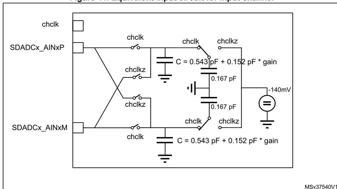
Note:
Gain can be from 0.5x to 8x (16x and 32x are digital gains)
Both chclk and chclkz are 0 when the channel is not active (not sampled) and both switch with opposite phases when the channel is active.
The average impedance during the channel conversion is:
Input equivalent circuit for external reference voltage (VREFSD+) input is shown in the next Figure.
Figure 42. Equivalent input circuit for VREFSD input
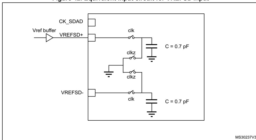
The diagram shows the equivalent input circuit for the VREFSD input of an SDADC. A Vref buffer is connected to the VREFSD+ input. The CK_SDAD input is connected to a clock signal (clk). The VREFSD+ input is connected to a switch that is controlled by the clk signal. The switch is connected to a capacitor C = 0.7 pF. The VREFSD- input is connected to a switch that is controlled by the clkz signal. The switch is connected to a capacitor C = 0.7 pF. The clkz signal is the inverted clock signal. The diagram is labeled MS30237V3.
The average impedance of external VREFSD+ input during SDADC operation is:
13.6 SDADC registers
Refer to Section 1.2 on page 36 for a list of abbreviations used in register descriptions.
13.6.1 Register write protection
Table 37. Register write protection
| ADON=1 | INITRDY=0 and ADON=1 | JCIP=1 | RCIP=1 | CALIBIP=1 | |
|---|---|---|---|---|---|
| RSYNC | - | ro | - | - | - |
| JSYNC | - | ro | - | - | - |
| PDI/SBI | ro | - | - | - | - |
| SLOWCK | ro | - | - | - | - |
| REFV | ro (1) | - | - | - | - |
| FAST | - | ro | - | - | - |
| RSWSTART | - | ignored (2) | - | ignored | - |
| JSWSTART | - | ignored (2) | ignored | - | - |
| JEXTEN | - | ro | - | - | - |
| JEXTSEL | - | ro | - | - | - |
| JDS | - | ro | - | - | - |
| STARTCALIB | - | ignored (2) | - | - | ignored |
| CALIBCNT | - | ro | - | - | - |
| SDADC_JCHGR | rwnz | rwnz | rwnz | rwnz | rwnz |
| SDADC_CONFxR | - | ro | - | - | - |
| SDADC_CONFCHRx | - | ro | - | - | - |
1. REFV can be modified only when all of the SDADC modules are disabled (ADON=0 for all SDADCs).
2. The “START” bits are ignored when INIT=1 (as soon as initialization mode is requested). All bits can be modified when ADON=0.
Table legend
ro = read only
rwnz = read and write-non-zero (writes of all-zero values are ignored)
blank = read and write (no protection)
13.6.2 SDADC control register 1 (SDADC_CR1)
Address offset: 0x00
Reset value: 0x0000 0000
| 31 | 30 | 29 | 28 | 27 | 26 | 25 | 24 | 23 | 22 | 21 | 20 | 19 | 18 | 17 | 16 |
|---|---|---|---|---|---|---|---|---|---|---|---|---|---|---|---|
| INIT | Res. | Res. | Res. | Res. | Res. | Res. | Res. | Res. | Res. | Res. | Res. | Res. | Res. | RDMAEN | JDMAEN |
| rw | rw | rw |
| 15 | 14 | 13 | 12 | 11 | 10 | 9 | 8 | 7 | 6 | 5 | 4 | 3 | 2 | 1 | 0 |
|---|---|---|---|---|---|---|---|---|---|---|---|---|---|---|---|
| RSYNC | JSYNC | Res. | PDI | SBI | SLOWCK | REFV[1:0] | Res. | Res. | Res. | ROVRIE | REOCI E | JOVRIE | JEOCI E | EOCALIE | |
| rw | rw | rw | rw | rw | rw | rw | rw | rw | rw | rw | rw | ||||
Bit 31 INIT : Initialization mode request
0: Initialization mode is disabled and many control and configuration registers are read only
1: Initialization mode has been requested and firmware must wait for INITRDY to become '1' to write to the control and configuration registers
When INIT=1, all requests to launch conversions (software, trigger, synchronized) or calibration are ignored.
Bits 30:17 Reserved, must be kept at reset value.
Bit 17 RDMAEN : DMA channel enabled to read data for the regular channel
0: The DMA channel is not enabled to read regular data
1: The DMA channel is enabled to read regular data
RDMAEN must not be '1' if JDMAEN=1.
Bit 16 JDMAEN : DMA channel enabled to read data for the injected channel group
0: The DMA channel is not enabled to read injected data
1: The DMA channel is enabled to read injected data
JDMAEN must not be '1' if RDMAEN=1.
Bit 15 RSYNC : Launch regular conversion synchronously with SDADC1
0: Do not launch a regular conversion synchronously with SDADC1
1: Launch a regular conversion in this SDADC at the same moment that a regular conversion is launched in SDADC1
This bit can be modified only when INITRDY=1 (SDADC_ISR) or ADON=0 (SDADC_CR2).
Bit 14 JSYNC : Launch a injected conversion synchronously with SDADC1
0: Do not launch injected conversion synchronously with SDADC1
1: Launch an injected conversion in this SDADC at the same moment that an injected conversion is launched in SDADC1
This bit can be modified only when INITRDY=1 (SDADC_ISR) or ADON=0 (SDADC_CR2).
Bit 13 Reserved, must be kept at reset value.
Bit 12 PDI : Enter power down mode when idle
0: Do not enter power down mode when the SDADC is idle
1: Enter Power down when idle
When the SDADC is in power down mode due to PDI=1 and a conversion is requested, the SDADC takes 100µs to stabilize before launching the conversion.
This bit can be modified only when ADON=0 (SDADC_CR2).
Bit 11 SBI : Enter Standby mode when idle
0: Do not put the SDADC in Standby mode when it is idle
1: Put the SDADC in Standby mode when it is idle
When the SDADC is in Standby mode and a conversion is requested, the SDADC takes 50µs to stabilize before launching the conversion.
Software must not write '1' to SBI at the same time that it writes '1' to PDI.
This bit can be modified only when ADON=0 (SDADC_CR2).
Bit 10 SLOWCK : Slow clock mode enable
0: Disable Slow mode
1: Enable Slow mode (where the SDADC clock frequency should be only 1.5MHz) allowing a lower level of current consumption as well as operation at a lower minimum voltage
This bit may be written only when ADON=0 (SDADC_CR2).
Bits 9:8 REFV[1:0] : Reference voltage selection
00: External reference where the VREFSD+ pin must be forced externally
01: Internal reference where the reference voltage is forced to the 1.2V bandgap voltage internally and the VREFSD+ pin must be connected externally to a capacitance coupled to VREFSD-
10: Internal reference where the reference voltage is forced to the 1.8V bandgap voltage internally and the VREFSD+ pin must be connected externally to a capacitance coupled to VREFSD-
11: Internal reference where the reference voltage is forced internally to VDDSDx and the VREFSD+ pin must be externally connected to a capacitance coupled to VREFSD-. See Section : Constrains on VDDSDx versus VREFSD voltage .
These bits are available only in the register set of SDADC1 and may be written only when ADON=0 (SDADC_CR2) for all SDADC modules.
Bits 7:5 Reserved, must be kept at reset value.
Bit 4 ROVRIE : Regular data overrun interrupt enable
0: Regular data overrun interrupt disabled
1: Regular data overrun interrupt enabled
Please see explanation of ROVRF in SDADC_ISR.
Bit 3 REOCIE : Regular end of conversion interrupt enable
0: Regular end of conversion interrupt disabled
1: Regular end of conversion interrupt enabled
Refer to the description of the REOCF bit in the SDADC_ISR register.
Bit 2 JOVRIE : Injected data overrun interrupt enable
0: Injected data overrun interrupt disabled
1: Injected data overrun interrupt enabled
Refer to the description of the JOVRF bit in the SDADC_ISR register.
Bit 1 JEOCIE : Injected end of conversion interrupt enable
0: Injected end of conversion interrupt disabled
1: Injected end of conversion interrupt enabled
Refer to the description of the JEOCF bit in the SDADC_ISR register.
Bit 0 EOCALIE : End of calibration interrupt enable
0: End of calibration interrupt disabled
1: End of calibration interrupt enabled
Refer to the description of the EOCAF bit in the SDADC_ISR register.
13.6.3 SDADC control register 2 (SDADC_CR2)
Address offset: 0x04
Reset value: 0x0000 0000
| 31 | 30 | 29 | 28 | 27 | 26 | 25 | 24 | 23 | 22 | 21 | 20 | 19 | 18 | 17 | 16 |
|---|---|---|---|---|---|---|---|---|---|---|---|---|---|---|---|
| Res. | Res. | Res. | Res. | Res. | Res. | Res. | FAST | RSW START | RCONT | Res. | Res. | RCH[3:0] | |||
| rw | rc_w1 | rw | rw | rw | rw | rw | |||||||||
| 15 | 14 | 13 | 12 | 11 | 10 | 9 | 8 | 7 | 6 | 5 | 4 | 3 | 2 | 1 | 0 |
|---|---|---|---|---|---|---|---|---|---|---|---|---|---|---|---|
| JSW START | JEXTEN[1:0] | Res. | Res. | JEXTSEL[2:0] | Res. | JDS | JCONT | START CALIB | Res. | CALIBCNT[1:0] | ADON | ||||
| rc_w1 | rw | rw | rw | rw | rw | rw | rw | rc_w1 | rw | rw | rw | ||||
Bits 31:25 Reserved, must be kept at reset value.
Bit 24 FAST : Fast conversion mode selection
0: Fast conversion mode disabled
1: Fast conversion mode enabled
When converting a single channel in continuous mode, having enabled fast mode causes each conversion (except for the first) to execute 3 times faster (taking 120 SDADC cycles rather than 360). This bit has no effect for conversions which are not continuous.
This bit can be modified only when INITRDY=1 (SDADC_ISR) or ADON=0 (SDADC_CR2).
Bit 23 RSWSTART : Software start of a conversion on the regular channel
0: Writing '0' has no effect
1: Writing '1' makes a request to start a conversion on the regular channel and causes RCIP to become '1'. If RCIP=1 already or if INIT=1, writing to RSWSTART has no effect
This bit is always read as '0'.
Bit 22 RCONT : Continuous mode selection for regular conversions
0: The regular channel is converted just once for each conversion request
1: The regular channel is converted repeatedly after each conversion request
Writing '0' to this bit while a continuous regular conversion is already in progress stops continuous mode after the conversion already in progress is finished.
Setting this bit to '1' has no effect on any regular conversion which is pending or already in progress.
Bits 21:20 Reserved, must be kept at reset value.
Bits 19:16 RCH[3:0] : Regular channel selection
0: Channel 0 is selected as regular channel
1: Channel 1 is selected as regular channel
...
8: Channel 8 is selected as regular channel
9-15: Reserved, these values are forbidden
Writing these bits when RCIP=1 takes effect when the next regular conversion begins. This is especially useful in continuous mode (when RCONT=1). It affects also regular conversions which are pending (due to stabilization or due to an ongoing injected conversion).
Bit 15 JSWSTART : Start a conversion of the injected group of channels
0: Writing '0' has no effect.
1: Writing '1' makes a request to convert the channels in the injected conversion group, causing JCAP to become '1' at the same time. If JCAP=1 already or if INIT=1, then writing to JSWSTART has no effect.
This bit is always read as '0'.
Bits 14:13 JEXTEN[1:0] : Trigger enable and trigger edge selection for injected conversions
00: Trigger detection is disabled
01: Each rising edge on the selected trigger makes a request to launch a injected conversion
10: Each falling edge on the selected trigger makes a request to launch a injected conversion
11: Both rising edges and falling edges on the selected trigger make requests to launch injected conversions
This bit can be modified only when INITRDY=1 (SDADC_ISR) or ADON=0 (SDADC_CR2).
Bits 12:11 Reserved, must be kept at reset value.
Bits 10:8 JEXTSEL[2:0] : Trigger signal selection for launching injected conversions
0x0-0x7: Trigger inputs selected by following table.
This bit can be modified only when INITRDY=1 (SDADC_ISR) or ADON=0 (SDADC_CR2).
| SDADC1 | SDADC2 | SDADC3 | |
|---|---|---|---|
| 0x00 | TIM13_CH1 | TIM17_CH1 | TIM16_CH1 |
| 0x01 | TIM14_CH1 | TIM12_CH1 | TIM12_CH2 |
| 0x02 | TIM15_CH2 | TIM2_CH3 | TIM2_CH4 |
| 0x03 | TIM3_CH1 | TIM3_CH2 | TIM3_CH3 |
| 0x04 | TIM4_CH1 | TIM4_CH2 | TIM4_CH3 |
| 0x05 | TIM19_CH2 | TIM19_CH3 | TIM19_CH4 |
| 0x06 | EXTI15 | EXTI15 | EXTI15 |
| 0x07 | EXTI11 | EXTI11 | EXTI11 |
Bit 7 Reserved, must be kept at reset value.
Bit 6 JDS : Delay start of injected conversions.
0: Injected conversions begin as soon as possible after the request
1: After a request for a injected conversion is made, the SDADC waits a fixed interval before launching the conversion, allowing time for any regular conversions which is already in progress to finish, and thus assuring that the timing of the launch is deterministic.
The delay is 500 ADC clocks, unless PDI=1 and SLOWCK=0, in which case the delay is 600 ADC clocks.
This bit can be modified only when INITRDY=1 (SDADC_ISR) or ADON=0 (SDADC_CR2).
Bit 5 JCONT : Continuous mode selection for injected conversions
0: The series of conversions which converts each selected channel (the scan sequence) is executed just once for each conversion request
1: The series of conversions for the injected group channels is repeated continuously, starting over with the lowest selected channel each time the highest selected channel finishes its conversion
Writing '0' to this bit while a continuous injected conversion is already in progress stops continuous mode after the conversion already in progress is finished. If an injected conversions is pending or is already in progress when this bit changes to '1', it does not become continuous.
Bit 4 STARTCALIB : Start calibration
0: Writing '0' has no effect
1: Writing '1' makes a request to start the calibration sequence, causing CALIBIP to become '1' at the same time
After the request is made, the calibration starts as soon as any ongoing activity (stabilization or a conversion) is finished, or immediately if the SDADC is stabilized and idle.
Writing this bit when CALIBIP=1 or when INIT=1 has no effect.
This bit is always read as '0'.
Bit 3 Reserved, must be kept at reset value.
Bits 2:1 CALIBCNT[1:0] : Number of calibration sequences to be performed (number of valid configurations)
0: One calibration sequence will be performed to calculate OFFSET0[11:0]
1: Two calibration sequences will be performed to calculate OFFSET0[11:0] and OFFSET1[11:0]
2: Three calibration sequences will be performed to calculate OFFSET0[11:0], OFFSET1[11:0], and OFFSET2[11:0]
3: Reserved, must not use this value
This bit can be modified only when INITRDY=1 (SDADC_ISR) or ADON=0 (SDADC_CR2).
Bit 0 ADON : SDADC enable
0: All SDADC functions are disabled. Power down mode is entered, and the flags and the data are cleared
1: SDADC is enabled.
When PDI=0, the SDADC exits power down mode and the 100us of stabilization are observed starting at the moment that ADON is set to '1'.
13.6.4 SDADC interrupt and status register (SDADC_ISR)
Address offset: 0x08
Reset value: 0x0000 0000
| 31 | 30 | 29 | 28 | 27 | 26 | 25 | 24 | 23 | 22 | 21 | 20 | 19 | 18 | 17 | 16 |
|---|---|---|---|---|---|---|---|---|---|---|---|---|---|---|---|
| INITRDY | Res. | Res. | Res. | Res. | Res. | Res. | Res. | Res. | Res. | Res. | Res. | Res. | Res. | Res. | Res. |
| r | |||||||||||||||
| 15 | 14 | 13 | 12 | 11 | 10 | 9 | 8 | 7 | 6 | 5 | 4 | 3 | 2 | 1 | 0 |
| STABIP | RCIP | JCIP | CALIBIP | Res. | Res. | Res. | Res. | Res. | Res. | Res. | ROVRF | REOCF | JOVRF | JEOCF | EOCALF |
| r | r | r | r | r | r | r | r | r |
Bit 31 INITRDY : Initialization mode is ready
0: The SDADC is not in initialization mode.
1: The SDADC is in initialization mode
Many control and configuration registers (see their descriptions) can be modified only when INITRDY=1.
Hardware clears this bit as soon as INIT (SDADC_CR1) is cleared.
Hardware sets this bit after the INIT bit is set. If a conversion or calibration is pending or ongoing when INIT is cleared, INITRDY stays at '0' until all operations have complete. Otherwise, INITRDY becomes '1' about two SDADC clock cycles after INIT is set.
Bits 30:16 Reserved, must be kept at reset value.
Bit 15 STABIP : Stabilization in progress status
0: The SDADC is either stabilized or it is in power down mode or Standby mode
1: The SDADC is currently in the process of stabilization, after waking up from either power down mode or Standby mode
A request to start the calibration sequence or to start a conversion can be issued while STABIP=1, with the actions automatically delayed until after stabilization is complete.
Bit 14 RCIP : Regular conversion in progress status
0: No request to convert the regular channel has been issued
1: The conversion of the regular channel is in progress or a request for a regular conversion is pending
A request to start a regular conversion is ignored when RCIP=1.
Bit 13 JCIP : Injected conversion in progress status
0: No request to convert the injected channel group (neither by software nor by trigger) has been issued
1: The conversion of the injected channel group is in progress or a request for a injected conversion is pending, due either to '1' being written to JSWSTART or to a trigger detection
A request to start a injected conversion is ignored when JCIP=1.
Bit 12 CALIBIP : Calibration in progress status
0: No calibration request has been issued
1: Calibration is in progress or a request to start calibration is pending
A request to start calibration is ignored when CALIBIP=1.
Bits 11:5 Reserved, must be kept at reset value.
Bit 4 ROVRF : Regular conversion overrun flag
0: No regular conversion overrun has occurred
1: A regular conversion overrun has occurred, which means that a regular conversion finished while REOCF was already '1'. RDATAR is not affected by overruns
This bit is set by hardware. It can be cleared by software using the CLRROVRF bit in the SDADC_CLRISR register.
Bit 3 REOCF : End of regular conversion flag
0: No regular conversion has completed
1: A regular conversion has completed and its data may be read
This bit is set by hardware. It is cleared when software reads SDADC_RDATAR.
Bit 2 JOVRF : Injected conversion overrun flag
0: No injected conversion overrun has occurred
1: A injected conversion overrun has occurred, which means that a injected conversion finished while JEOCF was already '1'. JDATAR is not affected by overruns
This bit is set by hardware. It can be cleared by software using the CLRJOVRF bit in the SDADC_CLRISR register.
Bit 1 JEOCF : End of injected conversion flag
0: No injected conversion has completed
1: A injected conversion has completed and its data may be read
This bit is set by hardware. It is cleared when software reads SDADC_JDATAR.
Bit 0 EOCALF : End of calibration flag
0: No calibration sequence has completed
1: Calibration has completed and the offsets have been updated
This bit is set by hardware. It can be cleared by software using the CLR EO CALF bit in SDADC_CLRISR.
Note: For each of the flag bits (ROVRF, REOCF, JOVRF, JEOCF, and EOCALF), an interrupt can be enabled by setting the corresponding bit in the SDADC_CR1 register. If an interrupt is requested, the flag must be cleared before exiting the interrupt service routine.
All the bits of SDADC_ISR except INITRDY are cleared automatically when ADON=0.
13.6.5 SDADC interrupt and status clear register (SDADC_CLRISR)
Address offset: 0x0C
Reset value: 0x0000 0000
| 31 | 30 | 29 | 28 | 27 | 26 | 25 | 24 | 23 | 22 | 21 | 20 | 19 | 18 | 17 | 16 |
|---|---|---|---|---|---|---|---|---|---|---|---|---|---|---|---|
| Res. | Res. | Res. | Res. | Res. | Res. | Res. | Res. | Res. | Res. | Res. | Res. | Res. | Res. | Res. | Res. |
| 15 | 14 | 13 | 12 | 11 | 10 | 9 | 8 | 7 | 6 | 5 | 4 | 3 | 2 | 1 | 0 |
| Res. | Res. | Res. | Res. | Res. | Res. | Res. | Res. | Res. | Res. | Res. | CLR ROVR F | Res. | CLR JOVRF | Res. | CLR EOCALF |
| rc_w1 | rc_w1 | rc_w1 |
Bits 31:5 Reserved, must be kept at reset value.
Bit 4 CLRROVRF : Clear the regular conversion overrun flag
0: Writing '0' has no effect
1: Writing '1' clears the ROVRF bit in the SDADC_ISR register
Bit 3 Reserved, must be kept at reset value.
Bit 2 CLRJOVRF : Clear the injected conversion overrun flag
0: Writing '0' has no effect
1: Writing '1' clears the JOVRF bit in the SDADC_ISR register
Bit 1 Reserved, must be kept at reset value.
Bit 0 CLREOCALF : Clear the end of calibration flag
0: Writing '0' has no effect
1: Writing '1' clears the EOCALF bit in the SDADC_ISR register
Note: The bits of SDADC_CLRISR are always read as '0'.
13.6.6 SDADC injected channel group selection register (SDADC_JCHGR)
Address offset: 0x14
Reset value: 0x0000 0001
| 31 | 30 | 29 | 28 | 27 | 26 | 25 | 24 | 23 | 22 | 21 | 20 | 19 | 18 | 17 | 16 |
|---|---|---|---|---|---|---|---|---|---|---|---|---|---|---|---|
| Res. | Res. | Res. | Res. | Res. | Res. | Res. | Res. | Res. | Res. | Res. | Res. | Res. | Res. | Res. | Res. |
| 15 | 14 | 13 | 12 | 11 | 10 | 9 | 8 | 7 | 6 | 5 | 4 | 3 | 2 | 1 | 0 |
| Res. | Res. | Res. | Res. | Res. | Res. | Res. | JCHG[8:0] | ||||||||
| rw | rw | rw | rw | rw | rw | rw | rw | rw | |||||||
Bits 31:9 Reserved, must be kept at reset value.
Bits 8:0 JCHG[8:0] : Injected channel group selection
0: If JCHG[i]=0, then channel i is not part of the injected group (where, \( 0 \le i \le 8 \) )
1: If JCHG[i]=1, then channel i is part of the injected group (where, \( 0 \le i \le 8 \) )
A injected conversion operates always in scan mode, which means that each of selected channels are converted, one after another. The lowest selected channel is converted first and the sequence ends at the highest selected channel.
If JCONT=1, this series of conversions is performed continuously.
If JCONT=1, FAST=1, and there is only one channel selected in the injected group, then each of the conversions (besides the first) finishes in only 120 SDADC cycles (rather than 360).
This field can be modified while an injected conversion is in progress and it will take effect for the next group conversion. Writing JCHG also affects injected conversions which are pending (due to stabilization or due to the delay caused by JDS=1).
At least one channel must always be selected for the injected group. Writes causing all JCHG bits to be zero are ignored.
13.6.7 SDADC configuration 0 register (SDADC_CONF0R)
This register specifies the parameters for configuration 0. If CONFCHi[1:0]='00', then each conversion of channel "i" will use the configuration settings specified in this register.
Address offset: 0x20
Reset value: 0x0000 0000
| 31 | 30 | 29 | 28 | 27 | 26 | 25 | 24 | 23 | 22 | 21 | 20 | 19 | 18 | 17 | 16 |
|---|---|---|---|---|---|---|---|---|---|---|---|---|---|---|---|
| COMMON0[1:0] | ] | Res. | Res. | SE0[1:0] | Res. | Res. | Res. | GAIN0[2:0] | Res. | Res. | Res. | Res. | |||
| rw | rw | rw | rw | rw | rw | rw | |||||||||
| 15 | 14 | 13 | 12 | 11 | 10 | 9 | 8 | 7 | 6 | 5 | 4 | 3 | 2 | 1 | 0 |
| Res. | Res. | Res. | Res. | OFFSET0[11:0] | |||||||||||
| rw | rw | rw | rw | rw | rw | rw | rw | rw | rw | rw | rw | ||||
Bits 31:30 COMMON0[1:0] : Common mode for configuration 0
00: Ground
01: VCM (VDD/2)
10: VDD
11: Reserved, must not use this value
This value is used only during calibration, i.e., when determining the offset. It has no direct effect on the conversions.
Bits 29:28 Reserved, must be kept at reset value.
Bits 27:26 SE0[1:0] : Single-ended mode for configuration 0
00: Conversions are executed in differential mode
01: Conversions are executed in single-ended offset mode
10: Reserved, do not use this setting
11: Conversions are executed in single-ended zero-volt reference mode
When this field is non-zero, the corresponding negative differential analog input, SDADCx_AINxM, is connected internally to VREFSD- so that its pin can be used for other functions.
Bits 25:23 Reserved, must be kept at reset value.
Bits 22:20 GAIN0[2:0] : Gain setting for configuration 0
000: 1x gain
001: 2x gain
010: 4x gain
011: 8x gain
100: 16x gain
101: 32x gain
111: 0.5x gain
Bits 19:12 Reserved, must be kept at reset value.
Bits 11:0 OFFSET0[11:0] : Twelve-bit calibration offset for configuration 0
For channels which select configuration 0, OFFSET0 is applied to the results of each conversion.
This value is automatically set during calibration.
Note: This register can be modified only when INITRDY=1 (SDADC_ISR) or ADON=0 (SDADC_CR2).
13.6.8 SDADC configuration 1 register (SDADC_CONF1R)
This register specifies the parameters for configuration 1. If CONFCHi[1:0]='01', then each conversion of channel "i" will use the configuration settings specified in this register.
Address offset: 0x24
Reset value: 0x0000 0000
| 31 | 30 | 29 | 28 | 27 | 26 | 25 | 24 | 23 | 22 | 21 | 20 | 19 | 18 | 17 | 16 |
|---|---|---|---|---|---|---|---|---|---|---|---|---|---|---|---|
| COMMON1 [1:0] | Res. | Res. | SE1[1:0] | Res. | Res. | Res. | GAIN1[2:0] | Res. | Res. | Res. | Res. | ||||
| rw | rw | rw | rw | rw | rw | rw | |||||||||
| 15 | 14 | 13 | 12 | 11 | 10 | 9 | 8 | 7 | 6 | 5 | 4 | 3 | 2 | 1 | 0 |
| Res. | Res. | Res. | Res. | OFFSET1[11:0] | |||||||||||
| rw | rw | rw | rw | rw | rw | rw | rw | rw | rw | rw | rw | ||||
Bits 31:30 COMMON1[1:0] : Common mode for configuration 1
00: Ground
01: VCM (VDD/2)
10: VDD
11: Reserved, must not use this value
This value is used only during calibration, i.e., when determining the offset. It has no direct effect on the conversions.
Bits 29:28 Reserved, must be kept at reset value.
Bits 27:26 SE1[1:0] : Single-ended mode for configuration 1
00: Conversions are executed in differential mode
01: Conversions are executed in single-ended offset mode
10: Reserved, do not use this setting
11: Conversions are executed in single-ended zero-volt reference mode
When this field is non-zero, the corresponding negative differential analog input, INNx, is connected internally to VREFSD- so that its pin can be used for other functions.
Bits 25:23 Reserved, must be kept at reset value.
Bits 22:20 GAIN1[2:0] : Gain setting for configuration 1
000: 1x gain
001: 2x gain
010: 4x gain
011: 8x gain
100: 16x gain
101: 32x gain
111: 0.5x gain
Bits 19:12 Reserved, must be kept at reset value.
Bits 11:0 OFFSET1[11:0] : Twelve-bit calibration offset for configuration 1
For channels which select configuration 1, OFFSET1 is applied to the results of each conversion.
This value is automatically set during calibration if CALIBCNT (SDADC_CR2) has a value greater than or equal to 1.
Note: This register can be modified only when INITRDY=1 (SDADC_ISR) or ADON=0 (SDADC_CR2).
13.6.9 SDADC configuration 2 register (SDADC_CONF2R)
This register specifies the parameters for configuration 2. If CONFCHi[1:0]='10', then each conversion of channel "i" will use the configuration settings specified in this register.
Address offset: 0x28
Reset value: 0x0000 0000
| 31 | 30 | 29 | 28 | 27 | 26 | 25 | 24 | 23 | 22 | 21 | 20 | 19 | 18 | 17 | 16 |
|---|---|---|---|---|---|---|---|---|---|---|---|---|---|---|---|
| COMMON2 [1:0] | Res. | Res. | SE2[1:0] | Res. | Res. | Res. | GAIN2[2:0] | Res. | Res. | Res. | Res. | ||||
| rw | rw | rw | rw | rw | rw | rw | |||||||||
| 15 | 14 | 13 | 12 | 11 | 10 | 9 | 8 | 7 | 6 | 5 | 4 | 3 | 2 | 1 | 0 |
| Res. | Res. | Res. | Res. | OFFSET2[11:0] | |||||||||||
| rw | rw | rw | rw | rw | rw | rw | rw | rw | rw | rw | rw | ||||
Bits 31:30 COMMON2[1:0] : Common mode for configuration 2
00: VSSSD
01: VDDSDx/2
10: VDDSDx
11: Reserved, this value is forbidden
This value is used only during calibration, i.e., when determining the offset. It has no direct effect on the conversions.
Bits 29:28 Reserved, must be kept at reset value.
Bits 27:26 SE2[1:0] : Single-ended mode for configuration 2
00: Conversions are executed in differential mode
01: Conversions are executed in single-ended offset mode
10: Reserved, do not use this setting
11: Conversions are executed in single-ended zero-volt reference mode
When this field is non-zero, the corresponding negative differential analog input, INNx, is connected internally to VREFSD- so that its pin can be used for other functions.
Bits 25:23 Reserved, must be kept at reset value.
Bits 22:20 GAIN2[2:0] : Gain setting for configuration 2
000: 1x gain
001: 2x gain
010: 4x gain
011: 8x gain
100: 16x gain
101: 32x gain
111: 0.5x gain
Bits 19:12 Reserved, must be kept at reset value.
Bits 11:0 OFFSET2[11:0] : Twelve-bit calibration offset for configuration 2
For channels which select configuration 2, OFFSET2 is applied to the results of each conversion.
This value is automatically set during calibration if CALIBCNT (SDADC_CR2) has a value greater than or equal to 2.
Note: This register can be modified only when INITRDY=1 (SDADC_ISR) or ADON=0 (SDADC_CR2).
13.6.10 SDADC channel configuration register 1 (SDADC_CONFCHR1)
This register specifies which configurations are to be used by channels 0-7.
Address offset: 0x40
Reset value: 0x0000 0000
| 31 | 30 | 29 | 28 | 27 | 26 | 25 | 24 | 23 | 22 | 21 | 20 | 19 | 18 | 17 | 16 |
|---|---|---|---|---|---|---|---|---|---|---|---|---|---|---|---|
| Res. | Res. | CONFCH7[1:0] | Res. | Res. | CONFCH6[1:0] | Res. | Res. | CONFCH5[1:0] | Res. | Res. | CONFCH4[1:0] | ||||
| rw | rw | rw | rw | rw | rw | rw | rw | ||||||||
| 15 | 14 | 13 | 12 | 11 | 10 | 9 | 8 | 7 | 6 | 5 | 4 | 3 | 2 | 1 | 0 |
| Res. | Res. | CONFCH3[1:0] | Res. | Res. | CONFCH2[1:0] | Res. | Res. | CONFCH1[1:0] | Res. | Res. | CONFCH0[1:0] | ||||
| rw | rw | rw | rw | rw | rw | rw | rw | ||||||||
CONFCHi[1:0]: Channel i configuration
00: Channel i uses the configuration specified in SDADC_CONF0R
01: Channel i uses the configuration specified in SDADC_CONF1R
10: Channel i uses the configuration specified in SDADC_CONF2R
11: Reserved, must not use this value
Note: This register can be modified only when INITRDY=1 (SDADC_ISR) or ADON=0 (SDADC_CR2).
13.6.11 SDADC channel configuration register 2 (SDADC_CONFCHR2)
This register specifies which configuration is to be used by channel 8.
Address offset: 0x44
Reset value: 0x0000 0000
| 31 | 30 | 29 | 28 | 27 | 26 | 25 | 24 | 23 | 22 | 21 | 20 | 19 | 18 | 17 | 16 |
|---|---|---|---|---|---|---|---|---|---|---|---|---|---|---|---|
| Res. | Res. | Res. | Res. | Res. | Res. | Res. | Res. | Res. | Res. | Res. | Res. | Res. | Res. | Res. | Res. |
| 15 | 14 | 13 | 12 | 11 | 10 | 9 | 8 | 7 | 6 | 5 | 4 | 3 | 2 | 1 | 0 |
| Res. | CONFCH8[1:0] | ||||||||||||||
| rw | rw | ||||||||||||||
Bits 31:2 Reserved, must be kept at reset value.
Bits 1:0 CONFCH8[1:0]: Channel 8 configuration
00: Channel 8 uses the configuration specified in SDADC_CONF0R
01: Channel 8 uses the configuration specified in SDADC_CONF1R
10: Channel 8 uses the configuration specified in SDADC_CONF2R
11: Reserved, must not use this value
Note: This register can be modified only when INITRDY=1 (SDADC_ISR) or ADON=0 (SDADC_CR2).
13.6.12 SDADC data register for injected group (SDADC_JDATAR)
This register contains the data resulting from the recently completed conversion of a channel in the injected group.
Address offset: 0x60
Reset value: 0x0000 0000
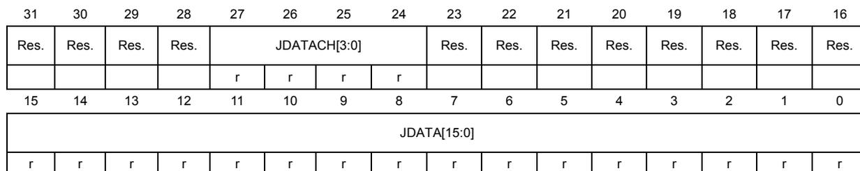
| 31 | 30 | 29 | 28 | 27 | 26 | 25 | 24 | 23 | 22 | 21 | 20 | 19 | 18 | 17 | 16 |
| Res. | Res. | Res. | Res. | JDATACH[3:0] | Res. | Res. | Res. | Res. | Res. | Res. | Res. | Res. | |||
| r | r | r | r | ||||||||||||
| 15 | 14 | 13 | 12 | 11 | 10 | 9 | 8 | 7 | 6 | 5 | 4 | 3 | 2 | 1 | 0 |
| JDATA[15:0] | |||||||||||||||
| r | r | r | r | r | r | r | r | r | r | r | r | r | r | r | r |
Bits 31:28 Reserved, must be kept at reset value.
Bits 27:24 JDATACH[3:0] : Injected channel most recently converted
When each conversion of a channel in the injected group finishes, JDATACH[3:0] is updated to indicate which channel was converted. This field is valid when JEOCF=1, and is set to zero when JEOCF is cleared. Thus, when JEOCF=1, JDATA[15:0] holds the data that corresponds to the channel indicated by JDATACH[3:0].
Bits 23:16 Reserved, must be kept at reset value.
Bits 15:0 JDATA[15:0] : Injected group conversion data
When each conversion of a channel in the injected group finishes, its resulting data is stored in this field. The data is valid when JEOCF=1. Reading this register clears both this field as well as the corresponding JEOCF.
Note: DMA may be used to read the data from this register. Half-word accesses may be used to read only the conversion data.
Note: This register is cleared as soon as it is read. Reading this register also clears JEOCF in SDADC_ISR. Thus, firmware must not read this register if DMA is activated to read data from this register.
13.6.13 SDADC data register for the regular channel (SDADC_RDATAR)
This register contains the data resulting from the recently completed conversion of the regular channel.
Address offset: 0x64
Reset value: 0x0000 0000
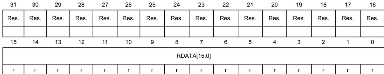
| 31 | 30 | 29 | 28 | 27 | 26 | 25 | 24 | 23 | 22 | 21 | 20 | 19 | 18 | 17 | 16 |
| Res. | Res. | Res. | Res. | Res. | Res. | Res. | Res. | Res. | Res. | Res. | Res. | Res. | Res. | Res. | Res. |
| 15 | 14 | 13 | 12 | 11 | 10 | 9 | 8 | 7 | 6 | 5 | 4 | 3 | 2 | 1 | 0 |
| RDATA[15:0] | |||||||||||||||
| r | r | r | r | r | r | r | r | r | r | r | r | r | r | r | r |
Bits 31:16 Reserved, must be kept at reset value.
Bits 15:0 RDATA[15:0] : Regular channel conversion data
When each regular conversion finishes, its data is stored in this register. The data is valid when REOCF=1. Reading this register clears both this field as well as the corresponding JEOCF.
Note: This register is cleared as soon as it is read. Reading this register also clears REOCF in SDADC_ISR.
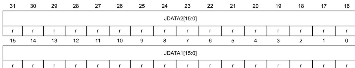
13.6.14 SDADC1 and SDADC2 injected data register (SDADC_JDATA12R)
This register contains the data resulting from the recently completed conversions of injected channels of SDADC1 and SDADC2. The data is a mirror image of the data in the corresponding SDADC_JDATAR registers. This register is available only in the set of registers for SDADC1 and must not be accessed unless the JSYNC bit of SDADC2 is set.
Address offset: 0x70
Reset value: 0x0000 0000
| 31 | 30 | 29 | 28 | 27 | 26 | 25 | 24 | 23 | 22 | 21 | 20 | 19 | 18 | 17 | 16 |
| JDATA2[15:0] | |||||||||||||||
| r | r | r | r | r | r | r | r | r | r | r | r | r | r | r | r |
| 15 | 14 | 13 | 12 | 11 | 10 | 9 | 8 | 7 | 6 | 5 | 4 | 3 | 2 | 1 | 0 |
| JDATA1[15:0] | |||||||||||||||
| r | r | r | r | r | r | r | r | r | r | r | r | r | r | r | r |
Bits 31:16 JDATA2[15:0] : Injected group conversion data for SDADC2
When each conversion of a channel in the injected group of SDADC2 finishes, its resulting data is stored in this field. The data is valid only when JEOCF of SDADC2 is set. Reading this register clears both this field as well as the corresponding JEOCF.
Bits 15:0 JDATA1[15:0] : Injected group conversion data for SDADC1
When each conversion of a channel in the injected group of SDADC1 finishes, its resulting data is stored in this field. The data is valid only when JEOCF of SDADC1 is set. Reading this register clears both this field as well as the corresponding JEOCF.
Note: DMA may be used to read the data from this register, in which case 32-bit word accesses must be used.
Note: This register is cleared as soon as it is read. Reading this register also clears JEOCF in the corresponding two SDADC_ISR registers. Thus, firmware must not read this register nor the SDADC_JDATA registers of SDADC1 and SDADC2 if DMA is activated to read data from this register.
13.6.15 SDADC1 and SDADC2 regular data register (SDADC_RDATA12R)
This register contains the data resulting from the recently completed conversions of regular channels of SDADC1 and SDADC2. The data is a mirror image of the data in the corresponding SDADC_RDATAR registers. This register is available only in the set of registers for SDADC1 and must not be accessed unless the RSYNC bit of SDADC2 is set.
Address offset: 0x74
Reset value: 0x0000 0000
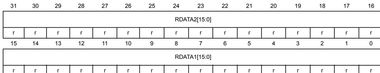
| 31 | 30 | 29 | 28 | 27 | 26 | 25 | 24 | 23 | 22 | 21 | 20 | 19 | 18 | 17 | 16 |
| RDATA2[15:0] | |||||||||||||||
| r | r | r | r | r | r | r | r | r | r | r | r | r | r | r | r |
| 15 | 14 | 13 | 12 | 11 | 10 | 9 | 8 | 7 | 6 | 5 | 4 | 3 | 2 | 1 | 0 |
| RDATA1[15:0] | |||||||||||||||
| r | r | r | r | r | r | r | r | r | r | r | r | r | r | r | r |
Bits 31:16 RDATA2[15:0] : Regular conversion data for SDADC2
When each conversion of the regular channel of SDADC2 finishes, its resulting data is stored in this field. The data is valid only when REOCF of SDADC2 is set. Reading this register clears both this field as well as the corresponding REOCF.
Bits 15:0 RDATA1[15:0] : Regular conversion data for SDADC1
When each conversion of the regular channel of SDADC1 finishes, its resulting data is stored in this field. The data is valid only when REOCF of SDADC1 is set. Reading this register clears both this field as well as the corresponding REOCF.
Note: DMA may be used to read the data from this register, in which case 32-bit word accesses must be used.
Note: This register is cleared as soon as it is read. Reading this register also clears REOCF in the corresponding two SDADC_ISR registers. Thus, firmware must not read this register nor the SDADC_RDATA registers of SDADC1 and SDADC2 if DMA is activated to read data from this register.
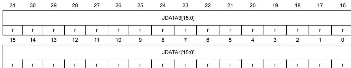
13.6.16 SDADC1 and SDADC3 injected data register (SDADC_JDATA13R)
This register contains the data resulting from the recently completed conversions of injected channels of SDADC1 and SDADC3. The data is a mirror image of the data in the corresponding SDADC_JDATAR registers. This register is available only in the set of registers for SDADC1 and must not be accessed unless the JSYNC bit of SDADC3 is set.
Address offset: 0x78
Reset value: 0x0000 0000
| 31 | 30 | 29 | 28 | 27 | 26 | 25 | 24 | 23 | 22 | 21 | 20 | 19 | 18 | 17 | 16 |
| JDATA3[15:0] | |||||||||||||||
| r | r | r | r | r | r | r | r | r | r | r | r | r | r | r | r |
| 15 | 14 | 13 | 12 | 11 | 10 | 9 | 8 | 7 | 6 | 5 | 4 | 3 | 2 | 1 | 0 |
| JDATA1[15:0] | |||||||||||||||
| r | r | r | r | r | r | r | r | r | r | r | r | r | r | r | r |
Bits 31:16 JDATA3[15:0] : Injected group conversion data for SDADC3
When each conversion of a channel in the injected group of SDADC3 finishes, its resulting data is stored in this field. The data is valid only when JEOCF of SDADC3 is set. Reading this register clears both this field as well as the corresponding JEOCF.
Bits 15:0 JDATA1[15:0] : Injected group conversion data for SDADC1
When each conversion of a channel in the injected group of SDADC1 finishes, its resulting data is stored in this field. The data is valid only when JEOCF of SDADC1 is set. Reading this register clears both this field as well as the corresponding JEOCF.
Note: DMA may be used to read the data from this register, in which case 32-bit word accesses must be used.
Note: This register is cleared as soon as it is read. Reading this register also clears JEOCF in the corresponding two SDADC_ISR registers. Thus, firmware must not read this register nor the SDADC_JDATA registers of SDADC1 and SDADC3 if DMA is activated to read data from this register.
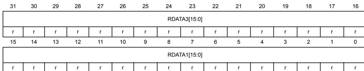
13.6.17 SDADC1 and SDADC3 regular data register (SDADC_RDATA13R)
This register contains the data resulting from the recently completed conversions of regular channels of SDADC1 and SDADC3. The data is a mirror image of the data in the corresponding SDADC_RDATAR registers. This register is available only in the set of registers for SDADC1 and must not be accessed unless the RSYNC bit of SDADC3 is set.
Address offset: 0x7C
Reset value: 0x0000 0000
| 31 | 30 | 29 | 28 | 27 | 26 | 25 | 24 | 23 | 22 | 21 | 20 | 19 | 18 | 17 | 16 |
| RDATA3[15:0] | |||||||||||||||
| r | r | r | r | r | r | r | r | r | r | r | r | r | r | r | r |
| 15 | 14 | 13 | 12 | 11 | 10 | 9 | 8 | 7 | 6 | 5 | 4 | 3 | 2 | 1 | 0 |
| RDATA1[15:0] | |||||||||||||||
| r | r | r | r | r | r | r | r | r | r | r | r | r | r | r | r |
Bits 31:16 RDATA3[15:0] : Regular conversion data for SDADC3
When each conversion of the regular channel of SDADC3 finishes, its resulting data is stored in this field. The data is valid only when REOCF of SDADC3 is set. Reading this register clears both this field as well as the corresponding REOCF.
Bits 15:0 RDATA1[15:0] : Regular conversion data for SDADC1
When each conversion of the regular channel of SDADC1 finishes, its resulting data is stored in this field. The data is valid only when REOCF of SDADC1 is set. Reading this register clears both this field as well as the corresponding REOCF.
Note: DMA may be used to read the data from this register, in which case 32-bit word accesses must be used.
Note: This register is cleared as soon as it is read. Reading this register also clears REOCF in the corresponding two SDADC_ISR registers. Thus, firmware must not read this register nor the SDADC_RDATA registers of SDADC1 and SDADC3 if DMA is activated to read data from this register.
13.6.18 SDADC register map
The following table summarizes the ADC registers.
Table 38. SDADC register map and reset values
| Offset | Register | 31 | 30 | 29 | 28 | 27 | 26 | 25 | 24 | 23 | 22 | 21 | 20 | 19 | 18 | 17 | 16 | 15 | 14 | 13 | 12 | 11 | 10 | 9 | 8 | 7 | 6 | 5 | 4 | 3 | 2 | 1 | 0 |
|---|---|---|---|---|---|---|---|---|---|---|---|---|---|---|---|---|---|---|---|---|---|---|---|---|---|---|---|---|---|---|---|---|---|
| 0x00 | SDADC_CR1 | INIT | Res. | Res. | Res. | Res. | Res. | Res. | Res. | Res. | Res. | Res. | Res. | Res. | Res. | RDMAEN | JDMAEN | RSYNC (1) | JSYNC (1) | Res. | Res. | SBI | SLOWCK | REFV[1:0] (2) | Res. | Res. | Res. | ROVRIE | REOCIE | JOVRIE | JEOCIE | EOCALIE | |
| Reset value | 0 | 0 | 0 | 0 | 0 | 0 | 0 | 0 | 0 | 0 | 0 | 0 | 0 | 0 | |||||||||||||||||||
| 0x04 | SDADC_CR2 | Res. | Res. | Res. | Res. | Res. | Res. | Res. | FAST | RSWSTART | RCONT | Res. | Res. | RCH [3:0] | JSWSTART | JEXTEN | Res. | Res. | JEXTSEL [3:0] | Res. | JDS | JCONT | STARTCALIB | Res. | CALIB CNT [1:0] | ADON | |||||||
| Reset value | 0 | 0 | 0 | 0 | 0 | 0 | 0 | 0 | 0 | 0 | 0 | 0 | 0 | 0 | 0 | 0 | 0 | 0 | 0 | 0 | |||||||||||||
| 0x08 | SDADC_ISR | INITRDY | Res. | Res. | Res. | Res. | Res. | Res. | Res. | Res. | Res. | Res. | Res. | Res. | Res. | Res. | Res. | STABIP | RCIP | JCIP | CALIBIP | Res. | Res. | Res. | Res. | Res. | Res. | Res. | ROVRF | REOCF | JOVRF | JEOCF | EOCALF |
| Reset value | 0 | 0 | 0 | 0 | 0 | 0 | 0 | 0 | 0 | 0 | |||||||||||||||||||||||
| 0x0C | SDADC_CLRISR | Res. | Res. | Res. | Res. | Res. | Res. | Res. | Res. | Res. | Res. | Res. | Res. | Res. | Res. | Res. | Res. | Res. | Res. | Res. | Res. | Res. | Res. | Res. | Res. | Res. | Res. | Res. | CLRROVRF | REOCF | CLRJOVRF | JEOCF | CLREOCALF |
| Reset value | 0 | 0 | 0 | ||||||||||||||||||||||||||||||
| 0x10 | Res. | ||||||||||||||||||||||||||||||||
| 0x14 | SDADC_JCHGR | Res. | Res. | Res. | Res. | Res. | Res. | Res. | Res. | Res. | Res. | Res. | Res. | Res. | Res. | Res. | Res. | Res. | Res. | Res. | Res. | Res. | Res. | JCHG[8:0] | |||||||||
| Reset value | 0 | 0 | 0 | 0 | 0 | 0 | 0 | 0 | 1 | ||||||||||||||||||||||||
| 0x18 | Res. | ||||||||||||||||||||||||||||||||
| 0x1C | Res. | ||||||||||||||||||||||||||||||||
| 0x20 | SDADC_CONF0R | COMMON0 [1:0] | Res. | Res. | SE0 [1:0] | Res. | Res. | Res. | Res. | Res. | GAIN0 [2:0] | Res. | Res. | Res. | Res. | Res. | Res. | Res. | Res. | Res. | Res. | OFFSET0[11:0] | |||||||||||
| Reset value | 0 0 | 0 0 | 0 0 0 | 0 | 0 | 0 | 0 | 0 | 0 | 0 | 0 | 0 | 0 | 0 | 0 | ||||||||||||||||||
| 0x24 | SDADC_CONF1R | COMMON1 [1:0] | Res. | Res. | SE1 [1:0] | Res. | Res. | Res. | Res. | Res. | GAIN1 [2:0] | Res. | Res. | Res. | Res. | Res. | Res. | Res. | Res. | Res. | Res. | OFFSET1[11:0] | |||||||||||
| Reset value | 0 0 | 0 0 | 0 0 0 | 0 | 0 | 0 | 0 | 0 | 0 | 0 | 0 | 0 | 0 | 0 | 0 | ||||||||||||||||||
| 0x28 | SDADC_CONF2R | COMMON2 [1:0] | Res. | Res. | SE2 [1:0] | Res. | Res. | Res. | Res. | Res. | GAIN2 [2:0] | Res. | Res. | Res. | Res. | Res. | Res. | Res. | Res. | Res. | Res. | OFFSET2[11:0] | |||||||||||
| Reset value | 0 0 | 0 0 | 0 0 0 | 0 | 0 | 0 | 0 | 0 | 0 | 0 | 0 | 0 | 0 | 0 | 0 | ||||||||||||||||||
| 0x2C - 0x3C | Res. | ||||||||||||||||||||||||||||||||
Table 38. SDADC register map and reset values (continued)
| Offset | Register | 31 | 30 | 29 | 28 | 27 | 26 | 25 | 24 | 23 | 22 | 21 | 20 | 19 | 18 | 17 | 16 | 15 | 14 | 13 | 12 | 11 | 10 | 9 | 8 | 7 | 6 | 5 | 4 | 3 | 2 | 1 | 0 |
|---|---|---|---|---|---|---|---|---|---|---|---|---|---|---|---|---|---|---|---|---|---|---|---|---|---|---|---|---|---|---|---|---|---|
| 0x40 | SDADC_CONFCHR1 | Res. | Res. | CON F CH7 [1:0] | Res. | Res. | CON F CH6 [1:0] | Res. | Res. | CON F CH5 [1:0] | Res. | Res. | CON F CH4 [1:0] | Res. | Res. | CON F CH3 [1:0] | Res. | Res. | CON F CH2 [1:0] | Res. | Res. | CON F CH1 [1:0] | Res. | Res. | CON F CH0 [1:0] | ||||||||
| Reset value | 0 0 | 0 0 | 0 0 | 0 0 | 0 0 | 0 0 | 0 0 | 0 0 | 0 0 | ||||||||||||||||||||||||
| 0x44 | SDADC_CONFCHR2 | Res. | Res. | Res. | Res. | Res. | Res. | Res. | Res. | Res. | Res. | Res. | Res. | Res. | Res. | Res. | Res. | Res. | Res. | Res. | Res. | Res. | Res. | Res. | Res. | Res. | Res. | Res. | Res. | Res. | Res. | Res. | CON F CH8 [1:0] |
| Reset value | 0 0 | ||||||||||||||||||||||||||||||||
| 0x48 - 0x5C | Res. | ||||||||||||||||||||||||||||||||
| 0x60 | SDADC_JDATAR | Res. | Res. | Res. | JDATAH [3:0] | Res. | Res. | Res. | Res. | Res. | Res. | Res. | Res. | Res. | Res. | JDATA[15:0] | |||||||||||||||||
| Reset value | 0 0 0 0 | 0 0 0 0 0 0 0 0 0 0 0 0 0 0 0 0 | |||||||||||||||||||||||||||||||
| 0x64 | SDADC_RDATAR | Res. | Res. | Res. | Res. | Res. | Res. | Res. | Res. | Res. | Res. | Res. | Res. | Res. | Res. | Res. | Res. | RDATA[15:0] | |||||||||||||||
| Reset value | 0 0 0 0 0 0 0 0 0 0 0 0 0 0 0 0 | ||||||||||||||||||||||||||||||||
| 0x68 - 0x6C | Res. | ||||||||||||||||||||||||||||||||
| 0x70 | SDADC_JDATA12R (2) | JDATA2[15:0] | |||||||||||||||||||||||||||||||
| Reset value | 0 0 0 0 0 0 0 0 0 0 0 0 0 0 0 0 | ||||||||||||||||||||||||||||||||
| 0x74 | SDADC_RDATA12R (2) | RDATA2[15:0] | |||||||||||||||||||||||||||||||
| Reset value | 0 0 0 0 0 0 0 0 0 0 0 0 0 0 0 0 | ||||||||||||||||||||||||||||||||
| 0x78 | SDADC_JDATA13R (2) | JDATA3[15:0] | |||||||||||||||||||||||||||||||
| Reset value | 0 0 0 0 0 0 0 0 0 0 0 0 0 0 0 0 | ||||||||||||||||||||||||||||||||
| 0x7C | SDADC_RDATA13R (2) | RDATA3[15:0] | |||||||||||||||||||||||||||||||
| Reset value | 0 0 0 0 0 0 0 0 0 0 0 0 0 0 0 0 | ||||||||||||||||||||||||||||||||
| 0x80 - 0xBC | Res. | ||||||||||||||||||||||||||||||||
1. Not available in SDADC1.
2. Available only in SDADC1.
Refer to Section 2.2 on page 40 for the register boundary addresses.