6. Power control (PWR)
6.1 Power supplies
An internal regulator is embedded in the STM32F373xx devices.
- • The internal regulator is enabled in the STM32F373xx MCUs:
The STM32F373xx devices require a 2.0 V - 3.6 V operating supply voltage ( \( V_{DD} \) ) and 2.0 V - 3.6 V analog supply voltage ( \( V_{DDA} \) ). The embedded regulator is used to supply the internal 1.8 V digital power. - • The internal regulator is disabled in the STM32F378xx MCUs:
The STM32F378xx devices require 1.8 V +/- 8 % operating voltage supply ( \( V_{DD} \) ) and 1.65 V - 3.6 V analog voltage supply ( \( V_{DDA} \) ). The embedded regulator is OFF and \( V_{DD} \) directly supplies the regulator output.
The real-time clock (RTC) and backup registers can be powered from the \( V_{BAT} \) voltage when the main \( V_{DD} \) supply is powered off.
Figure 7. Power supply overview
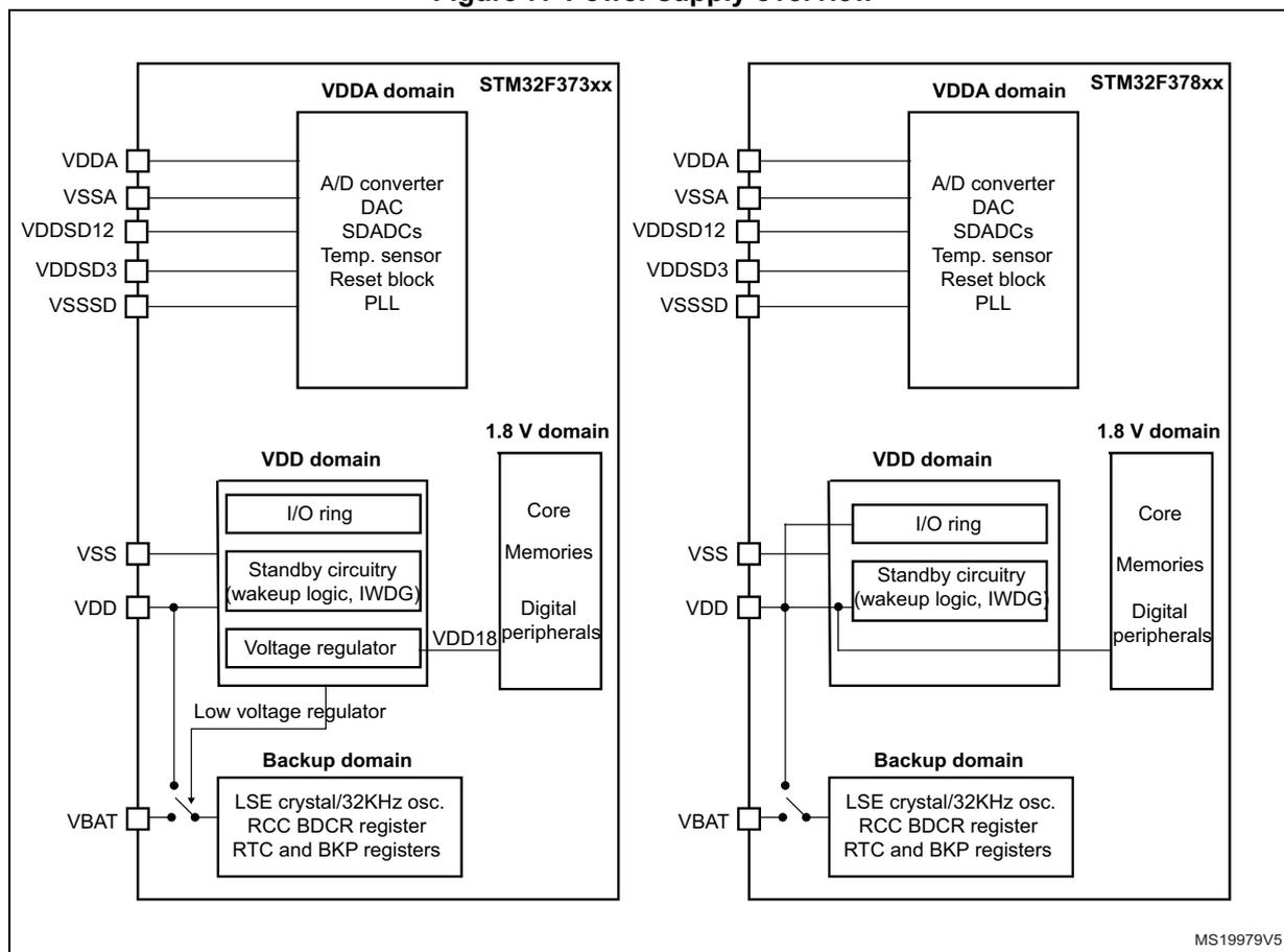
The diagram illustrates the power supply architecture for two STM32F37xxx device families. Both share a common VDDA domain with pins VDDA, VSSA, VDDSD12, VDDSD3, and VSSSD connected to a block containing an A/D converter, DAC, SDADCs, temperature sensor, reset block, and PLL. The VDD domain includes pins VSS and VDD connected to an I/O ring, standby circuitry (wakeup logic, IWDG), and a voltage regulator. The 1.8 V domain includes core, memories, and digital peripherals. The backup domain includes pins VBAT connected to an LSE crystal/32KHz oscillator, RCC BDCR register, RTC, and BKP registers. A low voltage regulator is also connected to VBAT. In the STM32F373xx diagram, the voltage regulator is active, supplying the 1.8 V domain. In the STM32F378xx diagram, the voltage regulator is disabled, and the 1.8 V domain is directly supplied by VDD.
MS19979V5
Supply voltages
- • \( V_{DD} \) , \( V_{SS} \) = 2.0 to 3.6 V: external power supply for I/Os (except I/Os related to SDADCs) and core.
These supply voltages are provided externally through \( V_{DD} \) and \( V_{SS} \) pins.
\( V_{DD} \) = 2.0 to 3.6 V (STM32F373xx devices) or 1.8 V \( \pm \) 8 % (STM32F378xx devices).
In the case of the 1.8 V mode external supply, \( V_{DD} \) directly supplies the regulator output, which directly drives the \( V_{DD18} \) domain. \( V_{DD} \) must always be kept lower or equal to \( V_{DDA} \) .
- • \( V_{DD18} \) = 1.65 to 1.95 V ( \( V_{DD18} \) domain): power supply for digital core, SRAM, and flash memory.
\( V_{DD18} \) is either internally generated through an internal voltage regulator (STM32F373xx devices) or can be provided directly from the external \( V_{DD} \) pin when the regulator is bypassed (STM32F378xx devices).
- • \( V_{DDA} \) , \( V_{SSA} \) = 2.4 to 3.6 V (ADC/DAC ON) or 1.65 to 3.6 V (both ADC/DAC OFF): external power supply for ADC, DAC, comparators, temperature sensor, PLL, HSI 8 MHz oscillator, and LSI 40 kHz oscillator.
It is forbidden to have \( V_{DDA} < V_{DD} - 0.4 \) V. An external Schottky diode must be placed between \( V_{DD} \) and \( V_{DDA} \) to guarantee this condition is met.
- • \( V_{BAT} \) = 1.65 to 3.6 V
Backup power supply for RTC, LSE oscillator, PC13 to PC15 and backup registers when \( V_{DD} \) is not present. When \( V_{DD} \) supply is present, the internal power switch switches the backup power to \( V_{DD} \) .
During fast \( V_{DD} \) startup, if \( V_{DD} + 0.6 > V_{BAT} \) , there is a 2 ms period of time during which the current can flow from \( V_{DD} \) to \( V_{BAT} \) pin.
In STM32F378xx devices, \( V_{BAT} \) must be connected to \( V_{DD} \) (no battery backup).
If \( V_{BAT} \) is not used, it must be connected to \( V_{DD} \) .
- • \( VDDSD12 \) = 2.2 to 3.6 V: external power supply for SDADC1/2, PB2, PB10, and PE7 to PE15 I/O pins (I/O pin ground is internally connected to \( V_{SS} \) ).
\( VDDSD12 \) must always be kept lower or equal to \( V_{DDA} \) . If \( VDDSD12 \) is not used, it must be connected to \( V_{DDA} \) .
- • \( VDDSD3 \) = 2.2 to 3.6 V: external power supply for SDADC3, PB14 to PB15 and PD8 to PD15 I/O pins (I/O pin ground is internally connected to \( V_{SS} \) ).
\( VDDSD3 \) must always be kept lower or equal to \( V_{DDA} \) . If \( VDDSD3 \) is not used, it must be connected to \( V_{DDA} \) .
- • \( VSSSD \) : analog ground pin for SDADC1/2/3.
\( VSSSD \) must be connected to the ground.
Note: PB0 and PB1 pins are powered from \( V_{DD} \) power supply. However, PB0 and PB1 are also sharing SDADC1 analog inputs. Therefore, the maximum voltage connected to these pins when they are not used as analog inputs must be less than the minimum of \( V_{DD} \) and \( VDDSD12 \) supply voltages to avoid current injection into \( V_{DD} \) and \( VDDSD12 \) .
When PB0 and PB1 are configured in analog input mode ( \( MODERy[1:0] = 11 \) , see Section 8.4.1: GPIO port mode register (GPIOx_MODER) (x = A to F) ), the maximum voltage must be less than \( VDDSD12 \) .
If \( V_{DD} \) is higher than \( VDDSD12 \) , it is forbidden to use PB0 and PB1 in digital output mode to avoid current injection from \( V_{DD} \) supply into \( VDDSD12 \) supply through shared analog inputs.
Reference voltages
- • \( V_{REF+} \) , \( V_{REF-} \) = 2.2 to 3.6 V
\( V_{REF+} \) and \( V_{REF-} \) correspond to the reference voltage for ADC and DAC peripherals. They define the ADC and DAC input range.
\( V_{REF+} \) must always be kept lower or equal to \( V_{DDA} \) . If \( V_{REF+} \) is not used, it must be connected to \( V_{DDA} \) and \( V_{REF-} \) must be connected to \( V_{SSA} \) .
\( V_{REF-} \) must be connected to the ground.
- • \( VREFSD+ \) , \( VREFSD- \) = 1.1 to 3.6 V
\( VREFSD+ \) and \( VREFSD- \) correspond to the reference voltage for SDADCx converters. They define the input conversion range for all SDADCx converters.
If SDADCx is configured in external reference voltage mode, the external voltage reference source must be connected to these pins.
If the external reference voltage is not enabled, then the selected SDADC internal reference voltage source ( \( V_{REFINT} \) , \( SDADC\_V_{DD} \) ) is present on \( VREFSD+ \) .
A 10 nF+1 µF capacitor must be placed between \( VREFSD+ \) and \( VREFSD- \) for decoupling purposes.
\( VREFSD+ \) must be lower than SDADC power supply:
\( VREFSD- \) must be connected to the ground.
6.1.1 Independent A/D and D/A converter supply and reference voltage
To improve conversion accuracy, the ADC and the DAC have an independent power supply, which can be separately filtered and shielded from noise on the PCB.
- • The ADC and DAC voltage supply input is available on a separate \( V_{DDA} \) pin.
- • An isolated supply ground connection is provided on pin \( V_{SSA} \) .
- • The SDADC voltage supply is available on separate \( VDDSDx \) pins.
- • An isolated SDADC supply ground connection is provided on pin \( VSSSD \) .
The \( V_{DDA} \) supply/reference voltage can be equal or higher than \( V_{DD} \) .
The \( VDDSD12 \) and \( VDDSD3 \) can be different from \( V_{DD} \) , \( V_{DDA} \) and from one another, considering they are inside the allowed working range and must always be lower than \( V_{DDA} \) . When \( VDDSD3 \) is different, it must start before or at the same time as \( VDDSD12 \) .
When a single supply is used, \( V_{DDA} \) , \( VDDSD12 \) and \( VDDSD3 \) can be externally connected to \( V_{DD} \) , through the external filtering circuit to ensure a noise free analog supply/reference voltage.
When \( V_{DDA} \) is different from \( V_{DD} \) , it must always be higher or equal to \( V_{DD} \) . To ensure this condition, also during power-up/power-down transitions, an external Schottky diode may be used between \( V_{DD} \) and \( V_{DDA} \) .
\( VDDSD12 \) and \( VDDSD3 \) can also be different, higher or lower than \( V_{DD} \) and lower or equal to \( V_{DDA} \) .
6.1.2 Correct grounding for analog applications
The STM32F37xxx devices feature several ground pins for various purposes. To properly design the PCB of the application, it is necessary to understand each ground pin function.
VSS ground
The VSS ground pin is used internally for all the digital parts: CPU, peripheral digital parts, GPIO pins. It is used both as a power supply and a digital signal reference for these parts.
All the digital currents flow through the VSS ground: supply currents and GPIO load currents. This is therefore a noisy ground and on a PCB, the above mentioned currents can produce voltage drops along the VSS ground path. The magnitude of the voltage drop depends on the VSS path design on the PCB. The low resistivity and low inductance paths are required, which leads to use one low-resistance PCB layer as VSS ground.
VSSA/VREF- ground
The VSSA ground pin is internally used as a supply voltage for the analog parts such as ADC, PLL, COMP and DAC. VSSA is also used as the reference voltage for ADC negative signal input (standard ADC uses single-ended mode with VSSA as reference ground) and DAC output signal. The VREF- ground is used as the ADC negative voltage reference input.
More analog currents flow through the VSSA ground: supply currents for ADC, DAC, COMP and PLL. These current changes are slow - not fast transient signals like in the digital part. The VSSA design is important for ADC and DAC, which uses VSSA as zero reference potential. For the ADC, it is recommended to use a star topology for the “negative” analog input signal path to prevent another current flow through this signal path (star topology into VSSA/VREF- pin).
The DAC output should have the ground reference (the “negative” output potential) sensed directly from the VSSA/VREF- pin.
To suppress noise from the digital application part, it is recommended to connect VSSA/VREF- to VSS near to the power supply source (star topology into the power supply source) and use decoupling capacitors between the VSSA pin and VDDA pin close to the microcontroller.
VSSSD ground
The VSSSD ground pin is used as a power supply for all SDADC peripherals (SDADC1, SDADC2 and SDADC3). VSSSD purpose is to provide a noise-free power supply to the high precision 16-bit SDADCs. The positive supply voltages (VDDSD12 and VDDSD3) purpose is the same.
It is recommended to connect the VSSSD pin to VSS close to the power supply source (star topology into the power supply source) and use decoupling capacitors between the VSSSD pin and the VDDSD12/VDDSD3 pins close to the microcontroller.
VREFSD- ground
The VREFSD- ground pin has two main functions. It is used primary as a negative reference input for all the SDADCs (SDADC1, SDADC2 and SDADC3), while the positive reference input is connected to the VREFSD+ pin. The VREFSD- pin is also used as a reference ground potential for the SDADC input configured in single-ended mode (in single ended configuration the negative SDADC input is connected internally to the VREFSD- pin).
For the SDADC single-ended input signals, it is recommended to use a star topology for the signal ground path. The signal ground is connected directly to the VREFSD- pin (star topology into the VREFSD- pin).
It is recommended to connect VREFSD- to VSS near to the power supply source (star topology into the power supply source) and to use decoupling capacitors between the VREFSD- pin and VREFSD+ pin close to the microcontroller.
Figure 8. Recommended SDADC grounding
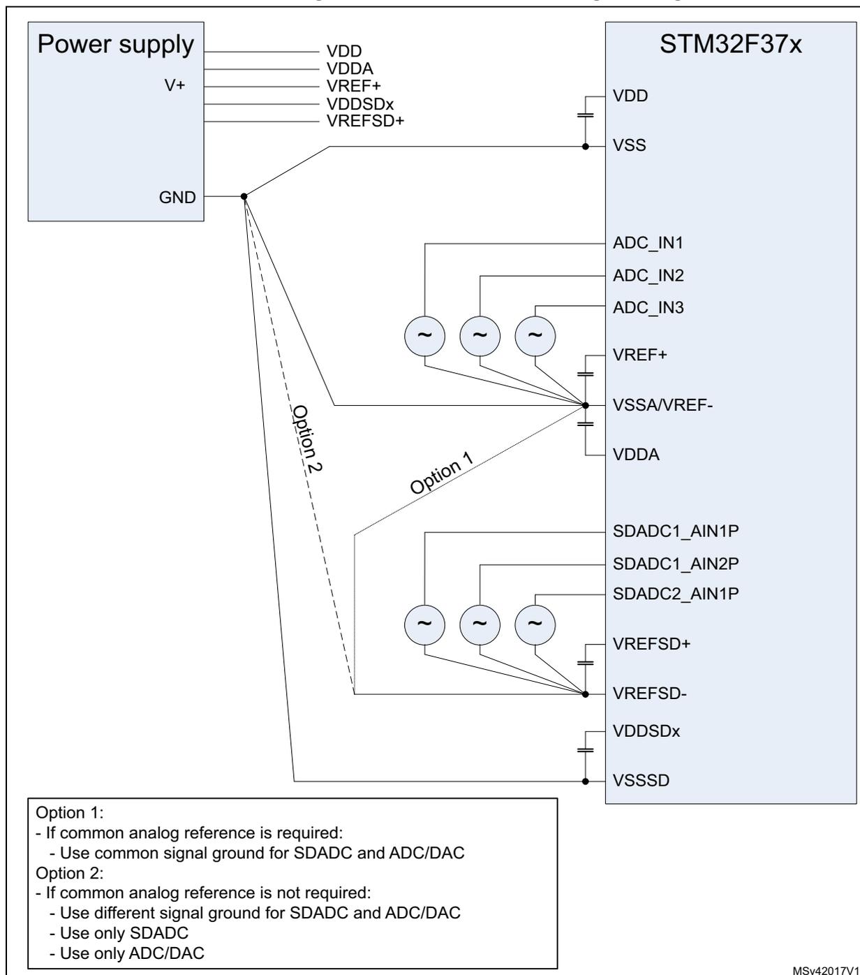
The diagram illustrates the recommended grounding for the STM32F37x microcontroller's SDADC and ADC pins. A power supply on the left provides V+, VDD, VDDA, VREF+, VDDSDx, VREFSD+, and GND. The microcontroller on the right has pins for VDD, VSS, ADC_IN1, ADC_IN2, ADC_IN3, VREF+, VSSA/VREF-, VDDA, SDADC1_AIN1P, SDADC1_AIN2P, SDADC2_AIN1P, VREFSD+, VREFSD-, VDDSDx, and VSSSD. Two options are shown for connecting the signal ground (GND) to the microcontroller's ground pins. Option 1 (solid line) connects GND to VSSA/VREF-, which is then connected to the ADC_IN1, ADC_IN2, and ADC_IN3 pins. Option 2 (dashed line) connects GND to VREFSD-, which is then connected to the SDADC1_AIN1P, SDADC1_AIN2P, and SDADC2_AIN1P pins. Both options include decoupling capacitors between VREF+ and VSSA/VREF-, and between VREFSD+ and VREFSD-.
Option 1:
- If common analog reference is required:
- Use common signal ground for SDADC and ADC/DAC
Option 2:
- If common analog reference is not required:
- Use different signal ground for SDADC and ADC/DAC
- Use only SDADC
- Use only ADC/DAC
MSv42017V1
6.1.3 Battery backup domain
To retain the content of the backup registers and supply the whole RTC domain when \( V_{DD} \) is turned off, \( V_{BAT} \) pin can be connected to an optional standby voltage supplied by a battery or by another source. The battery backup feature is not available on STM32F378xx microcontrollers ( \( V_{DD} = 1.8\text{ V} \pm 8\% \) ). When the device operates in this mode, \( V_{BAT} \) pin must be connected to \( V_{DD} \) .
The \( V_{BAT} \) pin powers the RTC unit, the LSE oscillator and the PC13 to PC15 I/Os, allowing the RTC to operate even when the main digital supply ( \( V_{DD} \) ) is turned off. The switch to the \( V_{BAT} \) supply is controlled by the Power Down Reset embedded in the Reset block.
Warning:
During
\(
t_{RSTTEMPO}
\)
(temporization at
\(
V_{DD}
\)
startup) or after a PDR is detected, the power switch between
\(
V_{BAT}
\)
and
\(
V_{DD}
\)
remains connected to
\(
V_{BAT}
\)
.
During the startup phase, if
\(
V_{DD}
\)
is established in less than
\(
t_{RSTTEMPO}
\)
(Refer to the datasheet for the value of
\(
t_{RSTTEMPO}
\)
) and
\(
V_{DD} > V_{BAT} + 0.6\text{ V}
\)
, a current may be injected into
\(
V_{BAT}
\)
through an internal diode connected between
\(
V_{DD}
\)
and the power switch (
\(
V_{BAT}
\)
).
If the power supply/battery connected to the
\(
V_{BAT}
\)
pin cannot support this current injection, it is strongly recommended to connect an external low-drop diode between this power supply and the
\(
V_{BAT}
\)
pin.
If no external battery is used in the application, it is recommended to connect \( V_{BAT} \) externally to \( V_{DD} \) with a 100 nF external ceramic decoupling capacitor (for more details refer to AN4206).
When the RTC domain is supplied by \( V_{DD} \) (analog switch connected to \( V_{DD} \) ), the following functions are available:
- • PC14 and PC15 can be used as either GPIO or LSE pins
- • PC13 can be used as GPIO, TAMPER pin, RTC Calibration Clock, RTC Alarm or second output (refer to Section 23.6.19: RTC backup registers (RTC_BKPxR) on page 556 )
Note: Due to the fact that the switch only sinks a limited amount of current (3 mA), the use of GPIOs PC13 to PC15 in output mode is restricted: the speed has to be limited to 2 MHz with a maximum load of 30 pF and these I/Os must not be used as a current source (for example, to drive a LED).
When the RTC domain is supplied by \( V_{BAT} \) (analog switch connected to \( V_{BAT} \) because \( V_{DD} \) is not present), the following functions are available:
- • PC14 and PC15 can be used as LSE pins only
- • PC13 can be used as a TAMPER pin, RTC Alarm or Second output (refer to section). Section 23.6.15: RTC calibration register (RTC_CALR) on page 550
6.1.4 Voltage regulator
The voltage regulator is always enabled after Reset. It works in three different modes depending on the application modes.
- • In Run mode, the regulator supplies full power to the 1.8 V domain (core, memories, and digital peripherals).
- • In Stop mode the regulator supplies low-power to the 1.8 V domain, preserving the contents of registers and SRAM. This mode is automatically disabled when the USART, CEC, or I2C peripheral requires a clock in Stop mode.
- • In Standby Mode, the regulator is powered off. The contents of the registers and SRAM are lost except for the Standby circuitry and the RTC Domain.
STM32F378xx microcontrollers
The internal voltage regulator is bypassed in STM32F378xx devices (unlike the STM32F373xx where the voltage regulator is functional). In this case, the microcontroller must be powered from a nominal \( V_{DD} = 1.8\text{ V} \pm 8\% \) voltage.
In STM32F378xx microcontrollers, the external NPOR input pin replaces the internal POR signal. The external NPOR pin must be controlled by the application (released after all supply voltages are stabilized) and be connected to \( V_{DDA} \) through a pull-up resistor. This pin replaces the PB2 GPIO pin.
6.2 Power supply supervisor
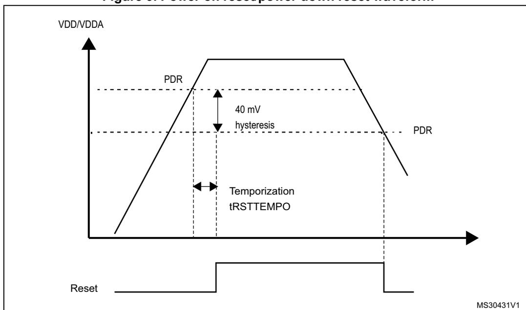
6.2.1 Power on reset (POR)/power down reset (PDR)
The device has an integrated power-on reset (POR) and power-down reset (PDR) circuits, which are always active and ensure proper operation above a threshold of 2 V.
The device remains in Reset mode when the monitored supply voltage is below a specified threshold, \( V_{POR/PDR} \) , without the need for an external reset circuit.
- • The POR monitors only the \( V_{DD}/V_{DDSD12} \) supply voltage. During the startup phase, \( V_{DDA} \) must arrive first and be higher than or equal to \( V_{DD} \) .
- • The PDR monitors all \( V_{DD}/V_{DDA}/V_{DDSD12} \) supply voltages. However, if the application is designed with \( V_{DDA}/V_{DDSD12} \) higher than or equal to \( V_{DD} \) , the \( V_{DDA} \) and \( V_{DDSD12} \) power supply supervisor can be disabled (by programming a dedicated \( V_{DDA\_MONITOR} \) and \( SDADC12\_VDD\_MONITOR \) option bits) to reduce the power consumption.
For more details on the power on /power down reset threshold, refer to the electrical characteristics section in the datasheet.
Figure 9. Power on reset/power down reset waveform
VDDSD12 monitoring
VDDSD12 supply is monitored comparing it with the internal reference voltage ( \( V_{REFINT} \) ). At startup, the supply voltage monitoring defaults to be active. It can then be disabled through the SDADC12_VDD_MONITOR option bit. Assuming \( V_{DDA} \) and \( V_{DD} \) are instantaneously available at startup, the system waits for VDDSD12 to exceed \( V_{REFINT} \) voltage before releasing the reset.
VDDSD3 is not monitored, so even if VDDSD12 is usually higher or lower than VDDSD3, the application has to make sure that VDDSD3 is set up before VDDSD12.
Constrains on VDDSDx versus VREFSD voltage
When the reference voltage for SDADC converters ( \( V_{REFSD+} \) ) is selected from SDADC power supply (REFV[1:0] bits of SDADC_CR1 register set to 11), the reference is provided by converters analog supplies (VDDSD12 and VDDSD3) and VDDSD12 must be at the same voltage level as VDDSD3.
Note: There is one exception if SDADC1 and SDADC2 converters are disabled and SDADC3 is enabled (through ENSDx bits in PWR_CR register and ADON bit in SDADC_CR2 register). In this case, VDDSD12 can be lower than VDDSD3 and the reference voltage can be provided by VDDSD3.
In STM32F378xx devices ( \( V_{DD}=1.8\text{ V} \pm 8\% \) ), VDDSD12 monitoring is OFF like the other supply voltage monitoring systems. This means that the application should take care of monitoring it externally and of releasing the external power on the NPOR reset pin after power-up and when all supply voltages are stable.
6.2.2 Programmable voltage detector (PVD)
You can use the PVD to monitor the \( V_{DD} \) power supply by comparing it to a threshold selected by the PLS[2:0] bits in the Power control register (PWR_CR) .
The PVD is enabled by setting the PVDE bit.
A PVDO flag is available, in the Power control/status register (PWR_CSR) , to indicate if \( V_{DD} \) is higher or lower than the PVD threshold. This event is internally connected to the EXTI line16 and can generate an interrupt if enabled through the EXTI registers. The PVD output interrupt can be generated when \( V_{DD} \) drops below the PVD threshold and/or when \( V_{DD} \) rises above the PVD threshold depending on the EXTI line16 rising/falling edge configuration. As an example, the service routine could perform emergency shutdown tasks.
Figure 10. PVD thresholds
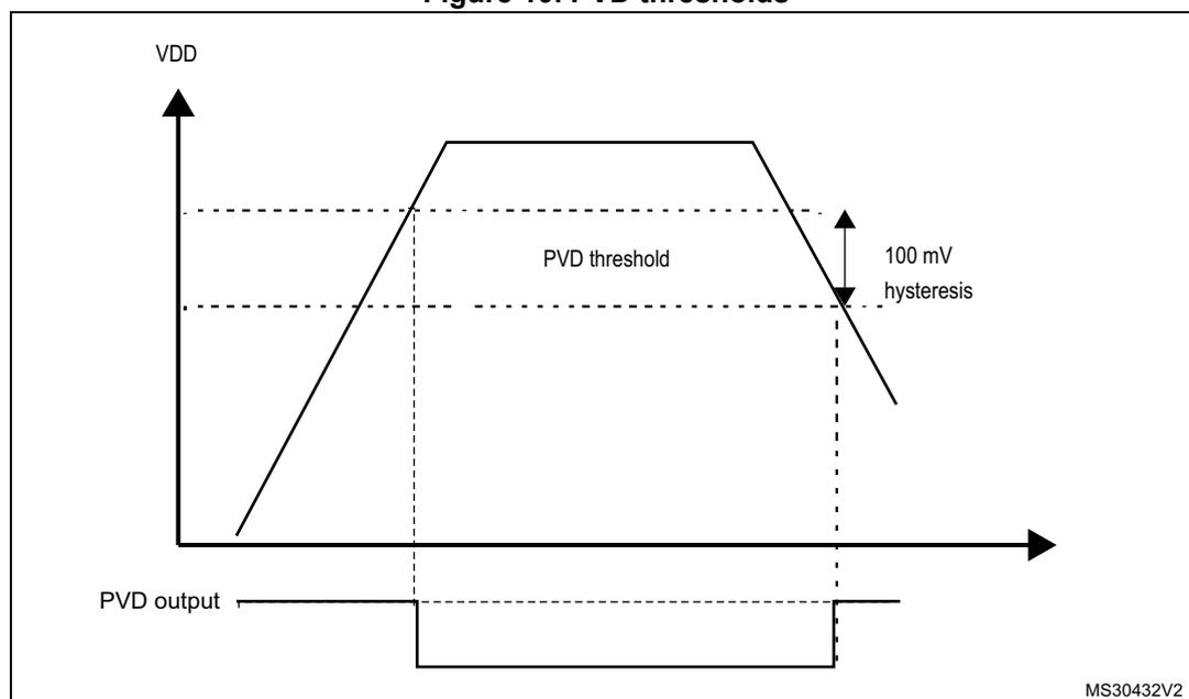
The figure illustrates the relationship between the supply voltage \( V_{DD} \) and the PVD output signal. The top part of the graph shows \( V_{DD} \) rising to a peak and then falling. The bottom part shows the PVD output signal, which is high (active) when \( V_{DD} \) is below the threshold and low (inactive) when \( V_{DD} \) is above the threshold. Two horizontal dashed lines represent the threshold levels, with a 100 mV hysteresis gap between them. Vertical dashed lines mark the points where \( V_{DD} \) crosses the thresholds, corresponding to the transitions in the PVD output signal. The label 'MS30432V2' is in the bottom right corner.
Note: In STM32F378xx devices ( \( V_{DD} = 1.8\text{ V} \pm 8\% \) ), the POR, PDR and PVD features are not available. The Power-on reset signal is applied on the NPOR pin. See details in the following section.
6.2.3 External NPOR signal
In STM32F378xx devices (powered from \( 1.8\text{ V} \pm 8\% \) ), the POR, PDR, and PVD features are not available and the application must provide the reset signal to the external NPOR pin. The NPOR signal is active low, and must be driven to \( V_{SS} \) when the \( V_{DDA} \) is applied. Then, when \( V_{DD} \) is stable, it can be released (high impedance) and the internal pull-up will hold this input to \( V_{DDA} \) . The NPOR signal can also be controlled by using an open-drain driver circuitry.
In STM32F378xx devices, PB2 I/O is not available and is replaced by the NPOR functionality.
6.3 Low-power modes
By default, the microcontroller is in Run mode after a system or a power Reset. Several low-power modes are available to save power when the CPU does not need to be kept running, for example when waiting for an external event. It is up to the user to select the mode that gives the best compromise between low-power consumption, short startup time and available wake-up sources.
The device features three low-power modes:
- • Sleep mode (CPU clock off, all peripherals including Cortex ® -M4 with FPU core peripherals like NVIC, SysTick, etc. are kept running)
- • Stop mode (all clocks are stopped)
- • Standby mode (1.8 V domain powered-off)
In addition, the power consumption in Run mode can be reduced by one of the following means:
- • Slowing down the system clocks
- • Gating the clocks to the APB and AHB peripherals when they are unused.
Table 13. Low-power mode summary
| Mode name | Entry | wakeup | Effect on 1.8 V domain clocks | Effect on V DD domain clocks | Voltage regulator |
|---|---|---|---|---|---|
| Sleep | WFI or Return from ISR | Any interrupt | CPU clock OFF no effect on other clocks or analog clock sources | None | ON |
| WFE | Wakeup event | ||||
| Stop | PDDS and LPDS bits + SLEEPDEEP bit + WFI or Return from ISR or WFE | Any EXTI line (configured in the EXTI registers) Specific communication peripherals on reception events (CEC, USART, I2C) | All 1.8V domain clocks OFF | HSI and HSE oscillators OFF | ON or in low-power mode (depends on Power control register (PWR_CR) ) (1) |
| PDDS bit + SLEEPDEEP bit + WFI or Return from ISR or WFE | WKUP pin rising edge, RTC alarm, external reset in NRST pin, IWDG reset | OFF |
1. In STM32F378xx devices, Standby mode is not available. Stop mode is still available, but it is meaningless to distinguish between voltage regulator in low-power mode and voltage regulator in Run mode, because the regulator is not used and V DD is applied externally to the regulator output.
6.3.1 Slowing down system clocks
In Run mode the speed of the system clocks (SYSCLK, HCLK, PCLK) can be reduced by programming the prescaler registers. These prescalers can also be used to slow down peripherals before entering Sleep mode.
For more details, refer to Section 7.4.2: Clock configuration register (RCC_CFGR) .
6.3.2 Peripheral clock gating
In Run mode, the HCLK and PCLK for individual peripherals and memories can be stopped at any time to reduce power consumption.
To further reduce power consumption in Sleep mode the peripheral clocks can be disabled prior to executing the WFI or WFE instructions.
Peripheral clock gating is controlled by the AHB peripheral clock enable register (RCC_AHBENR)
6.3.3 Low power modes
Entering low power mode
Low power modes are entered by the MCU by executing the WFI (Wait For Interrupt), or WFE (Wait for Event) instructions, or when the SLEEPONEXIT bit in the Cortex®-M4 with FPU System Control register is set on Return from ISR.
Exiting low power mode
From Sleep modes, and Stop modes the MCU exit low power mode depending on the way the low power mode was entered:
- • If the WFI instruction or Return from ISR was used to enter the low power mode, any peripheral interrupt acknowledged by the NVIC can wake up the device.
- • If the WFE instruction is used to enter the low power mode, the MCU exits the low power mode as soon as an event occurs. The wake-up event can be generated either by:
- – NVIC IRQ interrupt.
- - When SEVONPEND = 0 in the Cortex®-M4 with FPU System Control register. By enabling an interrupt in the peripheral control register and in the NVIC. When the MCU resumes from WFE, the peripheral interrupt pending bit and the NVIC peripheral IRQ channel pending bit (in the NVIC interrupt clear pending register) have to be cleared.
- – NVIC IRQ interrupt.
Only NVIC interrupts with sufficient priority will wake up and interrupt the MCU.
- When SEVONPEND = 1 in the Cortex®-M4 with FPU System Control register.
By enabling an interrupt in the peripheral control register and optionally in the NVIC. When the MCU resumes from WFE, the peripheral interrupt pending bit and when enabled the NVIC peripheral IRQ channel pending bit (in the NVIC interrupt clear pending register) have to be cleared.
All NVIC interrupts will wake up the MCU, even the disabled ones. Only enabled NVIC interrupts with sufficient priority will wake up and interrupt the MCU.
- – Event
Configuring an EXTI line in event mode. When the CPU resumes from WFE, it is not necessary to clear the EXTI peripheral interrupt pending bit or the NVIC IRQ channel pending bit as the pending bits corresponding to the event line is not set.
It may be necessary to clear the interrupt flag in the peripheral.
From Standby mode the MCU exit low power mode through an external reset (NRST pin), an IWDG reset, a rising edge on one of the enabled WKUPx pins or an RTC event occurs (see Figure 166: RTC block diagrams ).
After waking up from Standby mode, program execution restarts in the same way as after a Reset (boot pin sampling, option bytes loading, reset vector is fetched, etc.).
6.3.4 Sleep mode
Entering Sleep mode
The Sleep mode is entered according to Section : Entering low power mode , when the SLEEPDEEP bit in the Cortex ® -M4 with FPU System Control register is clear.
Refer to Table 14: Sleep for details on how to enter the Sleep mode.
Exiting Sleep mode
The Sleep mode is exit according to Section : Exiting low power mode .
Refer to Table 14: Sleep for more details on how to exit the Sleep mode.
Table 14. Sleep
| Sleep-now mode | Description |
|---|---|
| Mode entry | WFI (Wait for Interrupt) or WFE (Wait for Event) while: – SLEEPDEEP = 0 Refer to the Cortex ® -M4 with FPU System Control register. On return from ISR while: – SLEEPDEEP = 0 and – SLEEPONEXIT = 1 Refer to the Cortex ® -M4 with FPU System Control register. |
| Mode exit | If WFI or return from ISR was used for entry Interrupt: refer to Table 28: List of vectors If WFE was used for entry and SEVONPEND = 0: Wakeup event: refer to Section 11.2.3: Wake-up event management If WFE was used for entry and SEVONPEND = 1: Interrupt even when disabled in NVIC: refer to Table 28: List of vectors or Wakeup event: refer to Section 11.2.3: Wake-up event management |
| Wakeup latency | None |
6.3.5 Stop mode
The Stop mode is based on the Cortex ® -M4 with FPU deepsleep mode combined with peripheral clock gating. The voltage regulator can be configured either in normal or low-power mode in STM32F373xx devices. In STM32F378xx, it is meaningless to distinguish between voltage regulator in low-power mode and voltage regulator in Run mode, because the regulator is not used and V DD is applied externally to the regulator output..
In Stop mode, all clocks in the 1.8 V domain are stopped, the PLL, the HSI and the HSE RC oscillators are disabled, SRAM and register contents are preserved.
The I2C, CEC, and USART peripherals are an exception since they require a given kernel clock in Stop mode. In this case, when this specific clock request is ON, the power controller automatically forces the regulator to be ON as well, to prevent the device to operate in low-power mode since the regulator would not sustain the current required by the peripherals.
In the Stop mode, all I/O pins keep the same state as in Run mode.
Entering Stop mode
The Stop mode is entered according to Section : Entering low power mode , when the SLEEPDEEP bit in the Cortex ® -M4 with FPU System Control register is set.
Refer to Table 15 for details on how to enter the Stop mode.
To further reduce power consumption in Stop mode, the internal voltage regulator can be put in low-power mode. This is configured by the LPDS bit of the Power control register (PWR_CR) .
If flash memory programming is ongoing, the Stop mode entry is delayed until the memory access is finished.
If an access to the APB domain is ongoing, the Stop mode entry is delayed until the APB access is finished.
In Stop mode, the following features can be selected by programming individual control bits:
- • Independent watchdog (IWDG): the IWDG is started by writing to its Key register or by hardware option. Once started, it cannot be stopped, except by a Reset. See Section 21.3: IWDG functional description in Section 21: Independent watchdog (IWDG) .
- • real-time clock (RTC): this is configured by the RTCEN bit in the RTC domain control register (RCC_BDCR)
- • Internal RC oscillator (LSI RC): this is configured by the LSION bit in the Control/status register (RCC_CSR) .
- • External 32.768 kHz oscillator (LSE OSC): this is configured by the LSEON bit in the RTC domain control register (RCC_BDCR) .
The SDADC, ADC or DAC can also consume power during the Stop mode, unless they are disabled before entering it. To disable them, the ADON bit in the ADC_CR2 register and the ENx bit in the DAC_CR register must both be written to 0.
Note: If the application needs to disable the external oscillator (external clock) before entering Stop mode, the system clock source must be first switched to HSI and then clear the HSEON bit. Otherwise, if before entering Stop mode the HSEON bit is kept at 1, the security system (CSS) feature must be enabled to detect any external oscillator (external clock) failure and avoid a malfunction when entering Stop mode.
Exiting Stop mode
The Stop mode is exit according Section : Entering low power mode .
Refer to Table 15 for more details on how to exit Stop mode.
When exiting Stop mode by issuing an interrupt or a wake-up event, the HSI RC oscillator is selected as the system clock.
When the voltage regulator operates in low-power mode, an additional startup delay is incurred when waking up from Stop mode. By keeping the internal regulator ON during Stop mode, the consumption is higher although the startup time is reduced.
Table 15. Stop mode
| Stop mode | Description |
|---|---|
| Mode entry | WFI (Wait for Interrupt) or WFE (Wait for Event) while:
Note: To enter Stop mode, all EXTI Line pending bits (in Pending register (EXTI_PR)), all peripherals interrupt pending bits and RTC Alarm flag must be reset. Otherwise, the Stop mode entry procedure is ignored and program execution continues. On Return from ISR while:
Note: To enter Stop mode, all EXTI Line pending bits (in Pending register (EXTI_PR)), all peripherals interrupt pending bits and RTC Alarm flag must be reset. Otherwise, the Stop mode entry procedure is ignored and program execution continues. |
| Mode exit | If WFI or Return from ISR was used for entry:
Refer to Table 28: List of vectors . If WFE was used for entry and SEVONPEND = 0: Any EXTI Line configured in event mode. Refer to Section 11.2.3: Wake-up event management . If WFE was used for entry and SEVONPEND = 1: Any EXTI Line configured in Interrupt mode (even if the corresponding EXTI Interrupt vector is disabled in the NVIC). The interrupt source can be external interrupts or peripherals with wakeup capability. Refer to Table 28: List of vectors . Wakeup event: refer to Section 11.2.3: Wake-up event management |
| Wakeup latency | HSI RC wakeup time + regulator wakeup time from Low-power mode |
6.3.6 Standby mode
The Standby mode allows to achieve the lowest power consumption. It is based on the Cortex ® -M4 with FPU deepsleep mode, with the voltage regulator disabled. The 1.8 V domain is consequently powered off. The PLL, the HSI oscillator and the HSE oscillator are also switched off. SRAM and register contents are lost except for registers in the RTC domain (see Figure 7 ).
Caution: In the STM32F378xx devices, the Standby mode is not available.
Entering Standby mode
The Standby mode is entered according to Section : Entering low power mode , when the SLEEPDEEP bit in the Cortex ® -M4 with FPU System Control register is set.
Refer to Table 16 for more details on how to enter Standby mode.
In Standby mode, the following features can be selected by programming individual control bits:
- • Independent watchdog (IWDG): the IWDG is started by writing to its Key register or by hardware option. Once started, it cannot be stopped, except by a reset. See Section 21.3: IWDG functional description in Section 21: Independent watchdog (IWDG) .
- • real-time clock (RTC): this is configured by the RTCEN bit in the RTC domain control register (RCC_BDCR)
- • Internal RC oscillator (LSI RC): this is configured by the LSION bit in the Control/status register (RCC_CSR).
- • External 32.768 kHz oscillator (LSE OSC): this is configured by the LSEON bit in the RTC domain control register (RCC_BDCR)
Exiting Standby mode
The microcontroller exits the Standby mode when an external reset (NRST pin), an IWDG reset, a rising edge on the WKUP pin or the rising edge of an RTC alarm occurs (see Figure 166: RTC block diagram ). All registers are reset after wake-up from Standby except for Power control/status register (PWR_CSR) .
After waking up from Standby mode, program execution restarts in the same way as after a Reset (boot pins sampling, vector reset is fetched, etc.). The SBF status flag in the Power control/status register (PWR_CSR) indicates that the MCU was in Standby mode.
Refer to Table 16 for more details on how to exit Standby mode.
Table 16. Standby mode
| Standby mode | Description |
|---|---|
| Mode entry | WFI (Wait for Interrupt) or WFE (Wait for Event) while:
|
| Mode exit | WKUP pin rising edge, RTC alarm event's rising edge, external Reset in NRST pin, IWDG Reset. |
| Wakeup latency | Reset phase |
I/O states in Standby mode
In Standby mode, all I/O pins are high impedance except:
- • Reset pad (still available)
- • TAMPER pin if configured for tamper or calibration out
- • WKUP pin, if enabled
Debug mode
By default, the debug connection is lost if the application puts the MCU in Stop or Standby mode while the debug features are used. This is because the Cortex®-M4 with FPU core is no longer clocked.
However, by setting some configuration bits in the DBGMCU_CR register, the software can be debugged even when using the low-power modes extensively. For more details, refer to Section 31.16.1: Debug support for low-power modes .
6.3.7 Auto-wakeup from low-power mode
The RTC can be used to wake-up the MCU from low-power mode without depending on an external interrupt (Auto-wakeup mode). The RTC provides a programmable time base for waking up from Stop or Standby mode at regular intervals. For this purpose, two of the three alternative RTC clock sources can be selected by programming the RTCSEL[1:0] bits in the RTC domain control register (RCC_BDCR) :
- • Low-power 32.768 kHz external crystal oscillator (LSE OSC).
This clock source provides a precise time base with very low-power consumption (less than 1µA added consumption in typical conditions) - • Low-power internal RC Oscillator (LSI RC)
This clock source has the advantage of saving the cost of the 32.768 kHz crystal. This internal RC Oscillator is designed to add minimum power consumption.
To wake-up from Stop mode with an RTC alarm event, it is necessary to:
- • Configure the EXTI Line 17 to be sensitive to rising edge
- • Configure the RTC to generate the RTC alarm
To wake-up from Standby mode, there is no need to configure the EXTI Line 17.
6.4 Power control registers
The peripheral registers can be accessed by half-words (16-bit) or words (32-bit).
6.4.1 Power control register (PWR_CR)
Address offset: 0x00
Reset value: 0x0000 0000 (reset by wake-up from Standby mode)
| 31 | 30 | 29 | 28 | 27 | 26 | 25 | 24 | 23 | 22 | 21 | 20 | 19 | 18 | 17 | 16 |
|---|---|---|---|---|---|---|---|---|---|---|---|---|---|---|---|
| Res. | Res. | Res. | Res. | Res. | Res. | Res. | Res. | Res. | Res. | Res. | Res. | Res. | Res. | Res. | Res. |
| 15 | 14 | 13 | 12 | 11 | 10 | 9 | 8 | 7 | 6 | 5 | 4 | 3 | 2 | 1 | 0 |
| Res. | Res. | Res. | Res. | ENSD3 | ENSD2 | ENSD1 | DBP | PLS[2:0] | PVDE | CSBF | CWUF | PDDS | LPDS | ||
| rw | rw | rw | rw | rw | rw | rw | rw | rc_w1 | rc_w1 | rw | rw | ||||
Bits 31:12 Reserved, must be kept at reset value.
Bit 11 ENSD3 : Enable SDADC3.
This bit is set and cleared by software.
0: SDADC3 disabled. SDADC3 is in power down mode.
1: SD3 is enabled.
Bit 10 ENSD2 : Enable SDADC2.
This bit is set and cleared by software.
0: SDADC2 disabled. SDADC2 is in power down mode.
1: SD2 is enabled.
Bit 9 ENSD1 : Enable SDADC1.
This bit is set and cleared by software.
0: SDADC1 disabled. SDADC1 is in power down mode.
1: SD1 is enabled.
Bit 8 DBP : Disable RTC domain write protection.
In reset state, the RTC and backup registers are protected against parasitic write access. This bit must be set to enable write access to these registers.
0: Access to RTC and Backup registers disabled
1: Access to RTC and Backup registers enabled
Note: If the HSE divided by 128 is used as the RTC clock, this bit must remain set to 1.
Bits 7:5 PLS[2:0] : PVD level selection.
These bits are written by software to select the voltage threshold detected by the programmable voltage detector.
Note: 000: 2.2V
001: 2.3V
010: 2.4V
011: 2.5V
100: 2.6V
101: 2.7V
110: 2.8V
111: 2.9V
Note: Refer to the electrical characteristics of the datasheet for more details.
Note: Once the PVD_LOCK is enabled (for CLASS B protection) the PLS[2:0] bits cannot be programmed anymore.
Bit 4 PVDE : Programmable voltage detector enable.
This bit is set and cleared by software.
0: PVD disabled
1: PVD enabled
Bit 3 CSBF : Clear standby flag.
This bit is always read as 0.
0: No effect
1: Clear the SBF Standby Flag (write).
Bit 2 CWUF : Clear wakeup flag.
This bit is always read as 0.
0: No effect
1: Clear the WUF Wakeup Flag after 2 System clock cycles . (write)
Bit 1 PDDS : Power down deepsleep.
This bit is set and cleared by software. It works together with the LPDS bit.
0: Enter Stop mode when the CPU enters Deepsleep. The regulator status depends on the LPDS bit.
1: Enter Standby mode when the CPU enters Deepsleep.
Bit 0 LPDS : Low-power deepsleep.
This bit is set and cleared by software. It works together with the PDDS bit.
0: Voltage regulator on during Stop mode
1: Voltage regulator in low-power mode during Stop mode
6.4.2 Power control/status register (PWR_CSR)
Address offset: 0x04
Reset value: 0x0000 0000 (not reset by wakeup from Standby mode)
Additional APB cycles are needed to read this register versus a standard APB read.
| 31 | 30 | 29 | 28 | 27 | 26 | 25 | 24 | 23 | 22 | 21 | 20 | 19 | 18 | 17 | 16 |
|---|---|---|---|---|---|---|---|---|---|---|---|---|---|---|---|
| Res. | Res. | Res. | Res. | Res. | Res. | Res. | Res. | Res. | Res. | Res. | Res. | Res. | Res. | Res. | Res. |
| 15 | 14 | 13 | 12 | 11 | 10 | 9 | 8 | 7 | 6 | 5 | 4 | 3 | 2 | 1 | 0 |
| Res. | Res. | Res. | Res. | Res. | EWUP3 | EWUP2 | EWUP1 | Res. | Res. | Res. | Res. | VREFI NTRDYF | PVDO | SBF | WUF |
| rw | rw | rw | r | r | r | r |
Bits 31:11 Reserved, must be kept at reset value.
Bit 10 EWUP3 : Enable WKUP3 pin
This bit is set and cleared by software.
0: WKUP3 pin is used for general purpose I/O. An event on the WKUP3 pin does not wakeup the device from Standby mode.
1: WKUP3 pin is used for wakeup from Standby mode and forced in input pull down configuration (rising edge on WKUP3 pin wakes-up the system from Standby mode).
Note: This bit is reset by a system Reset.
Bit 9 EWUP2 : Enable WKUP2 pin
This bit is set and cleared by software.
0: WKUP2 pin is used for general purpose I/O. An event on the WKUP2 pin does not wakeup the device from Standby mode.
1: WKUP2 pin is used for wakeup from Standby mode and forced in input pull down configuration (rising edge on WKUP2 pin wakes-up the system from Standby mode).
Note: This bit is reset by a system Reset.
Bit 8 EWUP1 : Enable WKUP1 pin
This bit is set and cleared by software.
0: WKUP1 pin is used for general purpose I/O. An event on the WKUP1 pin does not wakeup the device from Standby mode.
1: WKUP1 pin is used for wakeup from Standby mode and forced in input pull down configuration (rising edge on WKUP1 pin wakes-up the system from Standby mode).
Note: This bit is reset by a system Reset.
Bits 7:4 Reserved, must be kept at reset value.
Bit 3 VREFINTRDY: VREFINT reference voltage ready.This bit is cleared and set by hardware.
This bit indicates the state of the internal reference voltage VREFINT. It is set when VREFINT is ready. It is reset during stabilization of VREFINT.
Note: This flag is useful only for the STM32F378xx product when working with external NPOR pin. In the STM32F373xx product, the internal POR waits for the VREFINT stabilization before releasing the reset.
Bit 2 PVDO: PVD outputThis bit is set and cleared by hardware. It is valid only if PVD is enabled by the PVDE bit.
0: \( V_{DD} \) is higher than the PVD threshold selected with the PLS[2:0] bits.
1: \( V_{DD} \) is lower than the PVD threshold selected with the PLS[2:0] bits.
Note: The PVD is stopped by Standby mode. For this reason, this bit is equal to 0 after Standby or reset until the PVDE bit is set.
Once the PVD is enabled and configured in the PWR_CR register, PVDO can be used to generate an interrupt through the Extended Interrupt/event controller.
Once the PVD_LOCK is enabled (for CLASS B protection) PVDO cannot be disabled anymore.
Bit 1 SBF: Standby flagThis bit is set by hardware and cleared only by a POR/PDR (power on reset/power down reset) or by setting the CSBF bit in the Power control register (PWR_CR)
0: Device has not been in Standby mode
1: Device has been in Standby mode
Bit 0 WUF: Wakeup flagThis bit is set by hardware and cleared by a system reset or by setting the CWUF bit in the Power control register (PWR_CR) .
0: No wakeup event occurred
1: A wakeup event was received from the WKUP pin or from the RTC alarm
Note: An additional wakeup event is detected if the WKUP pin is enabled (by setting the EWUP bit) when the WKUP pin level is already high.
6.4.3 PWR register map
The following table summarizes the PWR registers.
Table 17. PWR register map and reset values
| Offset | Register | 31 | 30 | 29 | 28 | 27 | 26 | 25 | 24 | 23 | 22 | 21 | 20 | 19 | 18 | 17 | 16 | 15 | 14 | 13 | 12 | 11 | 10 | 9 | 8 | 7 | 6 | 5 | 4 | 3 | 2 | 1 | 0 |
|---|---|---|---|---|---|---|---|---|---|---|---|---|---|---|---|---|---|---|---|---|---|---|---|---|---|---|---|---|---|---|---|---|---|
| 0x000 | PWR_CR | Res. | Res. | Res. | Res. | Res. | Res. | Res. | Res. | Res. | Res. | Res. | Res. | Res. | Res. | Res. | Res. | Res. | Res. | Res. | Res. | ENSD3 | ENSD2 | ENSD1 | DBP | PLS[2:0] | PVDE | CSBF | CWUF | PDDS | LPDS | ||
| Reset value | 0 | 0 | 0 | 0 | 0 | 0 | 0 | 0 | 0 | 0 | 0 | 0 | |||||||||||||||||||||
| 0x004 | PWR_CSR | Res. | Res. | Res. | Res. | Res. | Res. | Res. | Res. | Res. | Res. | Res. | Res. | Res. | Res. | Res. | Res. | Res. | Res. | Res. | Res. | Res. | EWUP3 | EWUP2 | EWUP1 | Res. | Res. | Res. | Res. | VREFINTRDYF | PVDO | SBF | WUF |
| Reset value | 0 | 0 | 0 | 0 | 0 | 0 | 0 | ||||||||||||||||||||||||||
Refer to Section 2.2 on page 40 for the register boundary addresses.