2. System architecture and memory overview
2.1 System architecture
The main system consists of:
- • Five masters:
- – Cortex ® -M4 with FPU core I-bus
- – Cortex ® -M4 with FPU core D-bus
- – Cortex ® -M4 with FPU core S-bus
- – GP-DMA1 and GP-DMA2 (general-purpose DMAs)
- • Five slaves:
- – Internal SRAM
- – Internal Flash memory (ICODE and DCODE)
- – AHB to APBx (APB1 or APB2), which connect all the APB peripherals
- – AHB dedicated to GPIO ports
These are interconnected using a multilayer AHB bus architecture as shown in Figure 1 :
Figure 1. System architecture
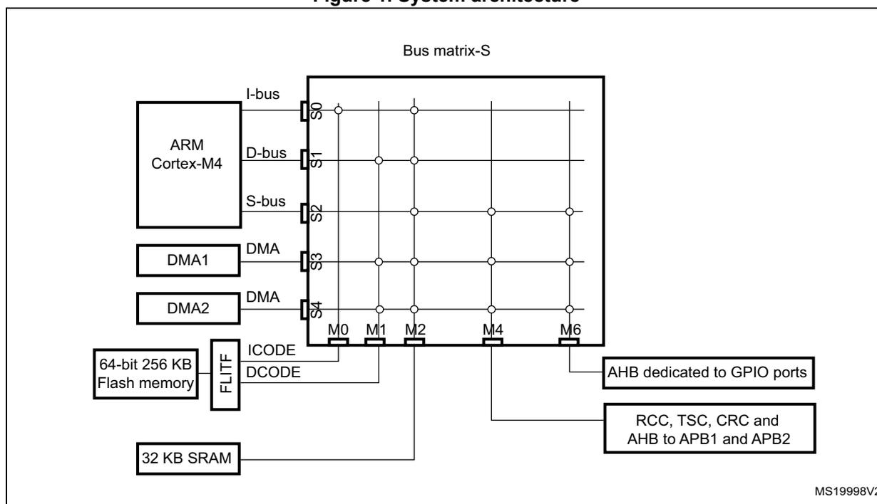
The diagram illustrates the system architecture centered around a 'Bus matrix-S'. On the left, five masters are shown: 'ARM Cortex-M4' (connected via I-bus, D-bus, and S-bus), 'DMA1' (connected via DMA), 'DMA2' (connected via DMA), '64-bit 256 KB Flash memory' (connected via ICODE and DCODE), and '32 KB SRAM'. The 'Bus matrix-S' is a grid with five columns labeled M0, M1, M2, M4, and M6 at the bottom. Connections are indicated by dots at the intersections of horizontal and vertical lines. On the right, the slaves are connected to the matrix: 'AHB dedicated to GPIO ports' to M0, 'RCC, TSC, CRC and AHB to APB1 and APB2' to M1, 'AHB to APBx' to M2, 'Internal Flash memory (ICODE and DCODE)' to M4, and 'Internal SRAM' to M6. A small code 'MS19998V2' is in the bottom right corner.
2.1.1 S0: I-bus
This bus connects the Instruction bus of the Cortex ® -M4 with FPU core to the BusMatrix. This bus is used by the core to fetch instructions. The target of this bus is a memory area (Flash and SRAM) containing the code.
2.1.2 S1: D-bus
This bus connects the Data bus of the Cortex®-M4 with FPU core to the BusMatrix. This bus is used by the core for literal load and debug access. The target of this bus is a memory area (Flash and SRAM) containing the code or data.
2.1.3 S2: S-bus
This bus connects the system bus of the Cortex®-M4 with FPU core to the BusMatrix. This bus is used to access data located in peripheral or SRAM area. Instructions can also be fetched on this bus even if it less efficient than the ICode bus.
The targets of this bus are the 32-Kbyte SRAM, the AHB2APB bridges, the AHB I/O port.
2.1.4 S3, S4: DMA-bus
This bus connects the AHB master interface of the DMAs to the BusMatrix which manages the access of different Masters to Flash memory, SRAM and AHB peripherals.
2.1.5 BusMatrix-S (5M5S)
The BusMatrix manages the access arbitration between Masters (core system bus, GP-DMAs). The arbitration scheme uses a Round Robin algorithm. The BusMatrix is composed of 5 slaves (FLASH ITF, SRAM, AHB2APB bridges and AHB I/O ports) and 5 masters (CPU System, DCODE and ICODE buses, DMA1 and DMA2 bus).
The following subsections describe all the peripherals connected to the AHB subsystem.
AHB/APB bridges
The two AHB/APB bridges provide full synchronous connections between the AHB and the 2 APB buses. APB1 is limited to 36 MHz, APB2 operates at full speed(72 MHz).
Refer to Section 2.2.2: Memory map and register boundary addresses on page 41 for the address mapping of the peripherals connected to this bridge.
After each device reset, all peripheral clocks are disabled (except for the SRAM and FLITF). Before using a peripheral you have to enable its clock in the RCC_AHBENR, RCC_APB2ENR or RCC_APB1ENR register.
Note: When a 16- or 8-bit access is performed on an APB register, the access is transformed into a 32-bit access: the bridge duplicates the 16- or 8-bit data to feed the 32-bit vector.
2.2 Memory organization
2.2.1 Introduction
Program memory, data memory, registers and I/O ports are organized within the same linear 4-Gbyte address space.
The bytes are coded in memory in Little Endian format. The lowest numbered byte in a word is considered the word's least significant byte and the highest numbered byte the most significant.
The addressable memory space is divided into eight main blocks, of 512 Mbytes each.
2.2.2 Memory map and register boundary addresses
Figure 2. Memory map
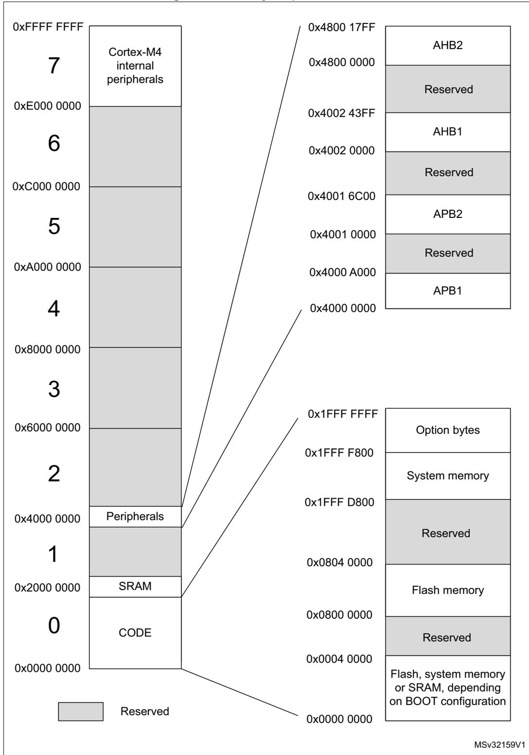
The memory map is divided into two main columns of address ranges. The left column shows the overall 32-bit address space from 0x0000 0000 to 0xFFFF FFFF, with major sections labeled 0 through 7. The right column provides a detailed view of specific memory regions, with lines connecting them to their positions in the overall space.
| Address Range | Memory Region / Feature |
|---|---|
| 0x0000 0000 – 0x0004 0000 | Flash, system memory or SRAM, depending on BOOT configuration |
| 0x0004 0000 – 0x0800 0000 | Reserved |
| 0x0800 0000 – 0x0804 0000 | Flash memory |
| 0x0804 0000 – 0x1FFF D800 | Reserved |
| 0x1FFF D800 – 0x1FFF F800 | System memory |
| 0x1FFF F800 – 0x1FFF FFFF | Option bytes |
| 0x4000 0000 – 0x4000 A000 | APB1 |
| 0x4000 A000 – 0x4001 0000 | Reserved |
| 0x4001 0000 – 0x4001 6C00 | APB2 |
| 0x4001 6C00 – 0x4002 0000 | Reserved |
| 0x4002 0000 – 0x4002 43FF | AHB1 |
| 0x4002 43FF – 0x4800 0000 | Reserved |
| 0x4800 0000 – 0x4800 17FF | AHB2 |
Legend: Reserved
MSv32159V1
All the memory map areas that are not allocated to on-chip memories and peripherals are considered “Reserved”. For the detailed mapping of available memory and register areas, refer to the following table.
The following table gives the boundary addresses of the peripherals available in the devices.
Table 1. STM32F37xxx peripheral register boundary addresses (1)
| Bus | Boundary address | Size | Peripheral | Peripheral register map |
|---|---|---|---|---|
| - | 0xE000 0000 - 0xE010 0000 | 1MB | Cortex®-M4 with FPU internal peripherals | - |
| - | 0x4800 1800 - 0x5FFF FFFF | ~384 MB | Reserved | - |
| AHB2 | 0x4800 1400 - 0x4800 17FF | 1KB | GPIOF | Section 8.4.11 on page 158 |
| 0x4800 1000 - 0x4800 13FF | 1KB | GPIOE | Section 8.4.11 on page 158 | |
| 0x4800 0C00 - 0x4800 0FFF | 1KB | GIOD | Section 8.4.11 on page 158 | |
| 0x4800 0800 - 0x4800 0BFF | 1KB | GPIOC | Section 8.4.11 on page 158 | |
| 0x4800 0400 - 0x4800 07FF | 1KB | GPIOB | Section 8.4.11 on page 158 | |
| 0x4800 0000 - 0x4800 03FF | 1KB | GPIOA | Section 8.4.11 on page 158 | |
| - | 0x4002 4400 - 0x47FF FFFF | ~128 MB | Reserved | - |
| AHB | 0x4002 4000 - 0x4002 43FF | 1 KB | TSC | Section 27.6.11 on page 766 |
| 0x4002 3400 - 0x4002 3FFF | 3 KB | Reserved | - | |
| 0x4002 3000 - 0x4002 33FF | 1 KB | CRC | Section 5.4.6 on page 78 | |
| 0x4002 2400 - 0x4002 2FFF | 3 KB | Reserved | - | |
| 0x4002 2000 - 0x4002 23FF | 1 KB | Flash memory interface | Section 3.2.1 on page 49 | |
| 0x4002 1400 - 0x4002 1FFF | 3 KB | Reserved | - | |
| 0x4002 1000 - 0x4002 13FF | 1 KB | RCC | Section 7.4.14 on page 141 | |
| 0x4002 0800 - 0x4002 0FFF | 2 KB | Reserved | - | |
| 0x4002 0400 - 0x4002 07FF | 1 KB | DMA2 | Section 10.6.7 on page 189 | |
| 0x4002 0000 - 0x4002 03FF | 1 KB | DMA1 | Section 10.6.7 on page 189 | |
| - | 0x4001 6C00 - 0x4001 FFFF | 37 KB | Reserved | - |
| Bus | Boundary address | Size | Peripheral | Peripheral register map |
|---|---|---|---|---|
| APB2 | 0x4001 6800 - 0x4001 6BFF | 1 KB | SDADC3 | Section 13.6.18 on page 267 |
| 0x4001 6400 - 0x4001 67FF | 1 KB | SDADC2 | Section 13.6.18 on page 267 | |
| 0x4001 6000 - 0x4001 63FF | 1 KB | SDADC1 | Section 13.6.18 on page 267 | |
| 0x4001 5C00 - 0x4001 5FFF | 1 KB | TIM19 | Section 16.5 on page 365 | |
| 0x4001 5800 - 0x4001 5BFF | 1 KB | DBGMCU | Section 31.18: DBG register map on page 891 | |
| 0x4001 4C00 - 0x4001 57FF | 4 KB | Reserved | - | |
| 0x4001 4800 - 0x4001 4BFF | 1 KB | TIM17 | Section 18.6.16 on page 484 | |
| 0x4001 4400 - 0x4001 47FF | 1 KB | TIM16 | Section 18.6.16 on page 484 | |
| 0x4001 4000 - 0x4001 43FF | 1 KB | TIM15 | Section 18.5.18 on page 465 | |
| 0x4001 3C00 - 0x4001 3FFF | 1 KB | Reserved | - | |
| 0x4001 3800 - 0x4001 3BFF | 1 KB | USART1 | Section 25.8.12 on page 689 | |
| 0x4001 3400 - 0x4001 37FF | 1 KB | Reserved | - | |
| 0x4001 3000 - 0x4001 33FF | 1 KB | SPI1/I2S1 | Section 26.9.10 on page 748 | |
| 0x4001 2800 - 0x4001 2FFF | 1 KB | Reserved | - | |
| 0x4001 2400 - 0x4001 27FF | 1 KB | ADC | Section 12.13 on page 228 | |
| 0x4001 0800 - 0x4001 23FF | 7 KB | Reserved | - | |
| 0x4001 0400 - 0x4001 07FF | 1 KB | EXTI | Section 11.3.7 on page 203 | |
| 0x4001 0000 - 0x4001 03FF | 1 KB | SYSCFG + COMP | Section 9.1.7 on page 167 and Section 15.5.2: COMP register map | |
| - | 0x4000 A000 - 0x4000 FFFF | 32 KB | Reserved | - |
| Bus | Boundary address | Size | Peripheral | Peripheral register map |
|---|---|---|---|---|
| APB1 | 0x4000 9C00 - 0x4000 9FFF | 1 KB | TIM18 | Section 20.4.9 on page 499 |
| 0x4000 9800 - 0x4000 9BFF | 1 KB | DAC2 | Section 14.10.15 on page 292 | |
| 0x4000 7C00 - 0x4000 97FF | 7 KB | Reserved | - | |
| 0x4000 7800 - 0x4000 7BFF | 1 KB | CEC | Section 30.7.7 on page 860 | |
| 0x4000 7400 - 0x4000 77FF | 1 KB | DAC1 | Section 14.10.15 on page 292 | |
| 0x4000 7000 - 0x4000 73FF | 1 KB | PWR | Section 6.4.3 on page 99 | |
| 0x4000 6800 - 0x4000 6FFF | 2 KB | Reserved | - | |
| 0x4000 6400 - 0x4000 67FF | 1 KB | CAN | Section 28.9.5 on page 807 | |
| 0x4000 6200 - 0x4000 63FF | 1 KB | Reserved | - | |
| 0x4000 6000 - 0x4000 61FF | 0.5 KB | USB packet (stored in SRAM) | Section 29.6.3 on page 841 | |
| 0x4000 5C00 - 0x4000 5FFF | 1 KB | USB FS | Section 29.6.3 on page 841 | |
| 0x4000 5800 - 0x4000 5BFF | 1 KB | I2C2 | Section 24.7 on page 610 | |
| 0x4000 5400 - 0x4000 57FF | 1 KB | I2C1 | Section 24.7 on page 610 | |
| 0x4000 4C00 - 0x4000 53FF | 2 KB | Reserved | - | |
| 0x4000 4800 - 0x4000 4BFF | 1 KB | USART3 | Section 25.8.12 on page 689 | |
| 0x4000 4400 - 0x4000 47FF | 1 KB | USART2 | Section 25.8.12 on page 689 | |
| 0x4000 4000 - 0x4000 43FF | 1 KB | Reserved | - | |
| 0x4000 3C00 - 0x4000 3FFF | 1 KB | SPI3/I2S3 | Section 26.9.10 on page 748 | |
| 0x4000 3800 - 0x4000 3BFF | 1 KB | SPI2/I2S2 | Section 26.9.10 on page 748 | |
| 0x4000 3400 - 0x4000 37FF | 1 KB | Reserved | - | |
| 0x4000 3000 - 0x4000 33FF | 1 KB | IWDG | Section 21.4.6 on page 508 | |
| 0x4000 2C00 - 0x4000 2FFF | 1 KB | WWDG | Section 22.5.4 on page 514 | |
| 0x4000 2800 - 0x4000 2BFF | 1 KB | RTC | Section 23.6.20 on page 556 | |
| APB1 | 0x4000 2400 - 0x4000 27FF | 1 KB | Reserved | - |
| 0x4000 2000 - 0x4000 23FF | 1 KB | TIM14 | Section 17.6.12 on page 412 | |
| 0x4000 1C00 - 0x4000 1FFF | 1 KB | TIM13 | Section 17.6.12 on page 412 | |
| 0x4000 1800 - 0x4000 1BFF | 1 KB | TIM12 | Section 17.5.13 on page 400 | |
| 0x4000 1400 - 0x4000 17FF | 1 KB | TIM7 | Section 20.4.9 on page 499 | |
| 0x4000 1000 - 0x4000 13FF | 1 KB | TIM6 | Section 20.4.9 on page 499 | |
| 0x4000 0C00 - 0x4000 0FFF | 1 KB | TIM5 | Section 16.5 on page 365 | |
| 0x4000 0800 - 0x4000 0BFF | 1 KB | TIM4 | Section 16.5 on page 365 | |
| 0x4000 0400 - 0x4000 07FF | 1 KB | TIM3 | Section 16.5 on page 365 | |
| 0x4000 0000 - 0x4000 03FF | 1 KB | TIM2 | Section 16.5 on page 365 | |
| - | 0x2000 8000 - 3FFF FFFF | ~512 MB | Reserved | - |
| - | 0x2000 0000 - 0x2000 7FFF | 32 KB | SRAM | - |
| Bus | Boundary address | Size | Peripheral | Peripheral register map |
|---|---|---|---|---|
| - | 0x1FFF FC00 - 0x1FFF FFFF | 1 KB | Reserved | - |
| - | 0x1FFF F800 - 0x1FFF FBFF | 1 KB | Option bytes | - |
| - | 0x1FFF D800 - 0x1FFF F7FF | 8 KB | System memory | - |
| - | 0x0801 0000 - 0x1FFF EBFF | ~384 MB | Reserved | - |
| - | 0x0800 0000 - 0x0803 FFFF | 256 KB | Main Flash memory | - |
| - | 0x0001 0000 - 0x07FF FFFF | 128 MB | Reserved | - |
| - | 0x0000 000 - 0x0000 FFFF | 64 KB | Main Flash memory, system memory or SRAM depending on BOOT configuration | - |
1. The gray color is used for reserved memory addresses.
2.3 Embedded SRAM
The STM32F37xxx features 32 Kbytes of static SRAM. It can be accessed as bytes, half-words (16 bits) or full words (32 bits). This memory can be addressed at maximum system clock frequency without wait state and thus by both CPU and DMA.
2.3.1 Parity check
The data bus width is 36 bits because 4 bits are available for parity check (1 bit per byte) to increase memory robustness, as required, for instance, by Class B or SIL norms.
The parity bits are computed and stored when writing into the SRAM. Then, they are automatically checked when reading. If one bit fails, an NMI is generated. The same error can also be linked to the BRK_IN Break input of TIMER1, with the SRAM_PARITY_LOCK control bit in the SYSCFG configuration register 2 (SYSCFG_CFGR2) . The SRAM Parity Error flag (SRAM_PEF) is available in the SYSCFG configuration register 2 (SYSCFG_CFGR2) .
2.4 Bit banding
The Cortex®-M4 memory map includes two bit-band regions. These regions map each word in an alias region of memory to a bit in a bit-band region of memory. Writing to a word in the alias region has the same effect as a read-modify-write operation on the targeted bit in the bit-band region.
In the STM32F37xxx both peripheral registers and SRAM are mapped in a bit-band region. This allows single bit-band write and read operations to be performed. The operations are only available for Cortex®-M4 accesses, not from other bus masters (for example, DMA).
A mapping formula shows how to reference each word in the alias region to a corresponding bit in the bit-band region. The mapping formula is:
where:
bit_word_addr is the address of the word in the alias memory region that maps to the targeted bit.
bit_band_base is the starting address of the alias region
byte_offset is the number of the byte in the bit-band region that contains the targeted bit
bit_number is the bit position (0-7) of the targeted bit.
Example:
The following example shows how to map bit 2 of the byte located at SRAM address 0x20000300 in the alias region:
Writing to address 0x22006008 has the same effect as a read-modify-write operation on bit 2 of the byte at SRAM address 0x20000300.
Reading address 0x22006008 returns the value (0x01 or 0x00) of bit 2 of the byte at SRAM address 0x20000300 (0x01: bit set; 0x00: bit reset).
For more information on bit-banding, refer to the Cortex®-M4 Technical Reference Manual .
2.5 Flash memory overview
The flash memory is composed of two distinct physical areas:
- • The main flash memory block. It contains the application program and user data if necessary.
- • The information block. It is composed of two parts:
- – Option bytes for hardware and memory protection user configuration.
- – System memory, which contains the proprietary bootloader code. Refer to Section 3: Embedded flash memory for more details .
Flash memory instructions and data access are performed through the AHB bus. The prefetch block is used for instruction fetches through the ICode bus. Arbitration is performed in the flash memory interface, and priority is given to data access on the DCode bus. It also implements the logic necessary to carry out the flash memory operations (Program/Erase) controlled through the flash registers.
2.6 Boot configuration
In the STM32F37xxx, three different boot modes can be selected through the BOOT0 pin and nBOOT1 bit in the User option byte, as shown in the following table:
Table 2. Boot modes
| Boot mode selection | Boot mode | Aliasings | |
|---|---|---|---|
| BOOT1 (inverted nBOOT1) | BOOT0 | - | - |
| x | 0 | Main Flash memory | Main flash memory is selected as boot space |
| 0 | 1 | System memory | System memory is selected as boot space |
| 1 | 1 | Embedded SRAM | Embedded SRAM (on the DCode bus) is selected as boot space |
The values on both BOOT0 pin and nBOOT1 option bit are latched on the 4th rising edge of SYSCLK after a reset.
It is up to the user to set the nBOOT1 and BOOT0 to select the required boot mode. The BOOT0 pin and nBOOT1 option bit are also resampled when exiting from Standby mode. Consequently, they must be kept in the required Boot mode configuration in Standby mode. After this startup delay has elapsed, the CPU fetches the top-of-stack value from address 0x0000 0000, then starts code execution from the boot memory at 0x0000 0004. Depending on the selected boot mode, main flash memory, system memory or SRAM is accessible as follows:
- • Boot from main flash memory: the main flash memory is aliased in the boot memory space (0x0000 0000), but still accessible from its original memory space (0x0800)
0000). In other words, the flash memory contents can be accessed starting from address 0x0000 0000 or 0x0800 0000.
- • Boot from system memory: the system memory is aliased in the boot memory space (0x0000 0000), but still accessible from its original memory space (0x1FFF D800).
- • Boot from the embedded SRAM: the SRAM is aliased in the boot memory space (0x0000 0000), but it is still accessible from its original memory space (0x2000 0000).
Embedded bootloader
The embedded bootloader is located in the System memory, programmed by ST during production. It is used to reprogram the flash memory through USART1 or USART2 or USB (DFU: device firmware upgrade).