33. Device electronic signature
The device electronic signature is stored in the System memory area of the Flash memory module, and can be read using the debug interface or by the CPU. It contains factory-programmed identification and calibration data that allow the user firmware or other external devices to automatically match to the characteristics of the STM32F0xx microcontroller.
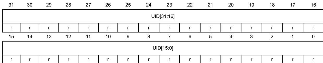
33.1 Unique device ID register (96 bits)
The unique device identifier is ideally suited:
- • for use as serial numbers (for example USB string serial numbers or other end applications)
- • for use as part of the security keys in order to increase the security of code in Flash memory while using and combining this unique ID with software cryptographic primitives and protocols before programming the internal Flash memory
- • to activate secure boot processes, etc.
The 96-bit unique device identifier provides a reference number which is unique for any device and in any context. These bits cannot be altered by the user.
Base address: 0x1FFF F7AC
Address offset: 0x00
Read only = 0xXXXX XXXX where X is factory-programmed
| 31 | 30 | 29 | 28 | 27 | 26 | 25 | 24 | 23 | 22 | 21 | 20 | 19 | 18 | 17 | 16 |
| UID[31:16] | |||||||||||||||
| r | r | r | r | r | r | r | r | r | r | r | r | r | r | r | r |
| 15 | 14 | 13 | 12 | 11 | 10 | 9 | 8 | 7 | 6 | 5 | 4 | 3 | 2 | 1 | 0 |
| UID[15:0] | |||||||||||||||
| r | r | r | r | r | r | r | r | r | r | r | r | r | r | r | r |
Bits 31:0 UID[31:0] : X and Y coordinates on the wafer expressed in BCD format
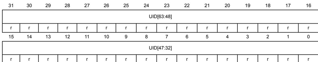
Address offset: 0x04
Read only = 0xXXXX XXXX where X is factory-programmed
| 31 | 30 | 29 | 28 | 27 | 26 | 25 | 24 | 23 | 22 | 21 | 20 | 19 | 18 | 17 | 16 |
| UID[63:48] | |||||||||||||||
| r | r | r | r | r | r | r | r | r | r | r | r | r | r | r | r |
| 15 | 14 | 13 | 12 | 11 | 10 | 9 | 8 | 7 | 6 | 5 | 4 | 3 | 2 | 1 | 0 |
| UID[47:32] | |||||||||||||||
| r | r | r | r | r | r | r | r | r | r | r | r | r | r | r | r |
Bits 31:8 UID[63:40] : LOT_NUM[23:0]
Lot number (ASCII encoded)
Bits 7:0 UID[39:32] : WAF_NUM[7:0]
Wafer number (8-bit unsigned number)
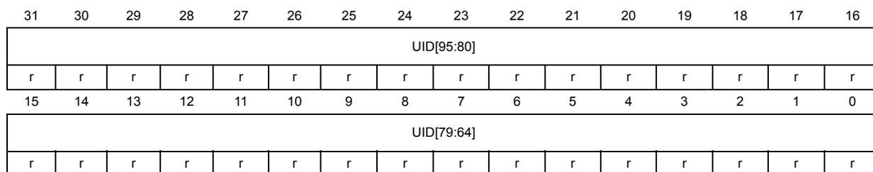
Address offset: 0x08
Read only = 0xXXXX XXXX where X is factory-programmed
| 31 | 30 | 29 | 28 | 27 | 26 | 25 | 24 | 23 | 22 | 21 | 20 | 19 | 18 | 17 | 16 |
| UID[95:80] | |||||||||||||||
| r | r | r | r | r | r | r | r | r | r | r | r | r | r | r | r |
| 15 | 14 | 13 | 12 | 11 | 10 | 9 | 8 | 7 | 6 | 5 | 4 | 3 | 2 | 1 | 0 |
| UID[79:64] | |||||||||||||||
| r | r | r | r | r | r | r | r | r | r | r | r | r | r | r | r |
Bits 31:0 UID[95:64] : LOT_NUM[55:24]
Lot number (ASCII encoded)
33.2 Flash memory size data register
Base address: 0x1FFF F7CC
Address offset: 0x00
Read only = 0xXXXX where X is factory-programmed

| 15 | 14 | 13 | 12 | 11 | 10 | 9 | 8 | 7 | 6 | 5 | 4 | 3 | 2 | 1 | 0 |
| FLASH_SIZE | |||||||||||||||
| r | r | r | r | r | r | r | r | r | r | r | r | r | r | r | r |
Bits 15:0 FLASH_SIZE[15:0] : Flash memory size
This bitfield indicates the size of the device Flash memory expressed in Kbytes.
As an example, 0x040 corresponds to 64 Kbytes.
Appendix A Code examples
A.1 Introduction
This appendix shows the code examples of the sequence described in this document.
These code examples are extracted from the STM32F0xx Snippet firmware package STM32SnippetsF0 available on www.st.com .
These code examples used the peripheral bit and register description from the CMSIS header file (stm32f0xx.h).
Code lines starting with // should be uncommented if the given register has been modified before.
A.2 Flash operation code examples
A.2.1 Flash memory unlocking sequence
/* (1) Wait till no operation is on going */
/* (2) Check that the Flash is unlocked */
/* (3) Perform unlock sequence */
while ((FLASH->SR & FLASH_SR_BSY) != 0) /* (1) */
{
    /* For robust implementation, add here time-out management */
}
if ((FLASH->CR & FLASH_CR_LOCK) != 0) /* (2) */
{
    FLASH->KEYR = FLASH_FKEY1; /* (3) */
    FLASH->KEYR = FLASH_FKEY2;
}
A.2.2 Main Flash programming sequence
/* (1) Set the PG bit in the FLASH_CR register to enable programming */
/* (2) Perform the data write (half-word) at the desired address */
/* (3) Wait until the BSY bit is reset in the FLASH_SR register */
/* (4) Check the EOP flag in the FLASH_SR register */
/* (5) clear it by software by writing it at 1 */
/* (6) Reset the PG Bit to disable programming */
FLASH->CR |= FLASH_CR_PG; /* (1) */
*(volatile uint16_t*)(flash_addr) = data; /* (2) */
while ((FLASH->SR & FLASH_SR_BSY) != 0) /* (3) */
{
    /* For robust implementation, add here time-out management */
}
if ((FLASH->SR & FLASH_SR_EOP) != 0) /* (4) */
{
FLASH->SR = FLASH_SR_EOP; /* (5) */
}
else
{
/* Manage the error cases */
}
FLASH->CR &= ~FLASH_CR_PG; /* (6) */A.2.3 Page erase sequence
/* (1) Set the PER bit in the FLASH_CR register to enable page erasing */
/* (2) Program the FLASH_AR register to select a page to erase */
/* (3) Set the STRT bit in the FLASH_CR register to start the erasing */
/* (4) Wait until the BSY bit is reset in the FLASH_SR register */
/* (5) Check the EOP flag in the FLASH_SR register */
/* (6) Clear EOP flag by software by writing EOP at 1 */
/* (7) Reset the PER Bit to disable the page erase */
FLASH->CR |= FLASH_CR_PER; /* (1) */
FLASH->AR = page_addr; /* (2) */
FLASH->CR |= FLASH_CR_STRT; /* (3) */
while ((FLASH->SR & FLASH_SR_BSY) != 0) /* (4) */
{
    /* For robust implementation, add here time-out management */
}
if ((FLASH->SR & FLASH_SR_EOP) != 0) /* (5) */
{
    FLASH->SR = FLASH_SR_EOP; /* (6) */
}
else
{
    /* Manage the error cases */
}
FLASH->CR &= ~FLASH_CR_PER; /* (7) */
A.2.4 Mass erase sequence
/* (1) Set the MER bit in the FLASH_CR register to enable mass erasing */
/* (2) Set the STRT bit in the FLASH_CR register to start the erasing */
/* (3) Wait until the BSY bit is reset in the FLASH_SR register */
/* (4) Check the EOP flag in the FLASH_SR register */
/* (5) Clear EOP flag by software by writing EOP at 1 */
/* (6) Reset the PER Bit to disable the mass erase */
FLASH->CR |= FLASH_CR_MER; /* (1) */
FLASH->CR |= FLASH_CR_STRT; /* (2) */
while ((FLASH->SR & FLASH_SR_BSY) != 0) /* (3) */
{
    /* For robust implementation, add here time-out management */
}

if ((FLASH->SR & FLASH_SR_EOP) != 0) /* (4) */
{
    FLASH->SR = FLASH_SR_EOP; /* (5) */
}
else
{
    /* Manage the error cases */
}
FLASH->CR &= ~FLASH_CR_MER; /* (6) */
A.2.5 Option byte unlocking sequence
/* (1) Wait till no operation is on going */
/* (2) Check that the Flash is unlocked */
/* (3) Perform unlock sequence for Flash */
/* (4) Check that the Option Bytes are unlocked */
/* (5) Perform unlock sequence for Option Bytes */
while ((FLASH->SR & FLASH_SR_BSY) != 0) /* (1) */
{
    /* For robust implementation, add here time-out management */
}
if ((FLASH->CR & FLASH_CR_LOCK) != 0) /* (2) */
{
    FLASH->KEYR = FLASH_FKEY1; /* (3) */
    FLASH->KEYR = FLASH_FKEY2;
}
if ((FLASH->CR & FLASH_CR_OPTWRE) == 0) /* (4) */
{
    FLASH->OPTKEYR = FLASH_OPTKEY1; /* (5) */
    FLASH->OPTKEYR = FLASH_OPTKEY2;
}
A.2.6 Option byte programming sequence
/* (1) Set the PG bit in the FLASH_CR register to enable programming */
/* (2) Perform the data write */
/* (3) Wait until the BSY bit is reset in the FLASH_SR register */
/* (4) Check the EOP flag in the FLASH_SR register */
/* (5) Clear the EOP flag by software by writing it at 1 */
/* (6) Reset the PG Bit to disable programming */
FLASH->CR |= FLASH_CR_OPTPG; /* (1) */
*opt_addr = data; /* (2) */
while ((FLASH->SR & FLASH_SR_BSY) != 0) /* (3) */
{
    /* For robust implementation, add here time-out management */
}
if ((FLASH->SR & FLASH_SR_EOP) != 0) /* (4) */
{
    FLASH->SR = FLASH_SR_EOP; /* (5) */
}
else
{
    /* Manage the error cases */
}
FLASH->CR &= ~FLASH_CR_OPTPG; /* (6) */
A.2.7 Option byte erasing sequence
/* (1) Set the OPTER bit in the FLASH_CR register to enable option byte
   erasing */
/* (2) Set the STRT bit in the FLASH_CR register to start the erasing */
/* (3) Wait until the BSY bit is reset in the FLASH_SR register */
/* (4) Check the EOP flag in the FLASH_SR register */
/* (5) Clear EOP flag by software by writing EOP at 1 */
/* (6) Reset the PER Bit to disable the page erase */
FLASH->CR |= FLASH_CR_OPTER; /* (1) */
FLASH->CR |= FLASH_CR_STRT; /* (2) */
while ((FLASH->SR & FLASH_SR_BSY) != 0) /* (3) */
{
    /* For robust implementation, add here time-out management */
}
if ((FLASH->SR & FLASH_SR_EOP) != 0) /* (4) */
{
    FLASH->SR = FLASH_SR_EOP; /* (5) */
}
else
{
    /* Manage the error cases */
}
FLASH->CR &= ~FLASH_CR_OPTER; /* (6) */
A.3 Clock controller
A.3.1 HSE start sequence code example
/**
 * Description: This function enables the interrupt on HSE ready,
 *              and start the HSE as external clock.
 */
__INLINE void StartHSE(void)
{
    /* Configure NVIC for RCC */
    /* (1) Enable Interrupt on RCC */
    /* (2) Set priority for RCC */
    NVIC_EnableIRQ(RCC_CRS_IRQn); /* (1) */
    NVIC_SetPriority(RCC_CRS_IRQn, 0); /* (2) */

    /* (1) Enable interrupt on HSE ready */
    /* (2) Enable the CSS
       Enable the HSE and set HSEBYP to use the external clock
       instead of an oscillator
       Enable HSE */
    /* Note : the clock is switched to HSE in the RCC_CRS_IRQHandler ISR */
    RCC->CIR |= RCC_CIR_HSERDYIE; /* (1) */
    RCC->CR |= RCC_CR_CSSON | RCC_CR_HSEBYP | RCC_CR_HSEON; /* (2) */
}

/**
 * Description: This function handles RCC interrupt request
 *              and switch the system clock to HSE.
 */
void RCC_CRS_IRQHandler(void)
{
    /* (1) Check the flag HSE ready */
    /* (2) Clear the flag HSE ready */
    /* (3) Switch the system clock to HSE */

    if ((RCC->CIR & RCC_CIR_HSERDYF) != 0) /* (1) */
    {
        RCC->CIR |= RCC_CIR_HSERDYC; /* (2) */
        RCC->CFGR = ((RCC->CFGR & (~RCC_CFGR_SW)) | RCC_CFGR_SW_0); /* (3) */
    }
    else
    {
        /* Report an error */
    }
}
A.3.2 PLL configuration modification code example
/* (1) Test if PLL is used as System clock */
/* (2) Select HSI as system clock */
/* (3) Wait for HSI switched */
/* (4) Disable the PLL */
/* (5) Wait until PLLRDY is cleared */
/* (6) Set the PLL multiplier to 6 */
/* (7) Enable the PLL */
/* (8) Wait until PLLRDY is set */
/* (9) Select PLL as system clock */
/* (10) Wait until the PLL is switched on */
if ((RCC->CFGR & RCC_CFGR_SWS) == RCC_CFGR_SWS_PLL) /* (1) */
{
    RCC->CFGR &= (uint32_t) (~RCC_CFGR_SW); /* (2) */
    while ((RCC->CFGR & RCC_CFGR_SWS) != RCC_CFGR_SWS_HSI) /* (3) */
    {
        /* For robust implementation, add here time-out management */
    }
}
RCC->CR &= (uint32_t) (~RCC_CR_PLLON); /* (4) */
while ((RCC->CR & RCC_CR_PLLRDY) != 0) /* (5) */
{
    /* For robust implementation, add here time-out management */
}
RCC->CFGR = RCC->CFGR & (~RCC_CFGR_PLLMUL) | (RCC_CFGR_PLLMUL6); /* (6) */
RCC->CR |= RCC_CR_PLLON; /* (7) */
while ((RCC->CR & RCC_CR_PLLRDY) == 0) /* (8) */
{
    /* For robust implementation, add here time-out management */
}
RCC->CFGR |= (uint32_t) (RCC_CFGR_SW_PLL); /* (9) */
while ((RCC->CFGR & RCC_CFGR_SWS) != RCC_CFGR_SWS_PLL) /* (10) */
{
    /* For robust implementation, add here time-out management */
}
A.3.3 MCO selection code example
/* Select system clock to be output on the MCO without prescaler */
RCC->CFGR |= RCC_CFGR_MCO_SYSCLK;
A.3.4 Clock measurement configuration with TIM14 code example
/**
 * Description: This function configures the TIM14 as input capture
 *              and enables the interrupt on TIM14
 */
__INLINE void ConfigureTIM14asInputCapture(void)
{
    /* (1) Enable the peripheral clock of Timer 14 */
    /* (2) Select the active input TI1, Program the input filter, and prescaler
     */
    /* (3) Enable interrupt on Capture/Compare */
    RCC->APB1ENR |= RCC_APB1ENR_TIM14EN; /* (1) */
    TIM14->CCMR1 |= TIM_CCMR1_IC1F_0 | TIM_CCMR1_IC1F_1 \
        | TIM_CCMR1_CC1S_0 | TIM_CCMR1_IC1PSC_1; /* (2) */
    TIM14->DIER |= TIM_DIER_CC1IE; /* (3) */

    /* Configure NVIC for TIM14 */
    /* (4) Enable Interrupt on TIM14 */
    /* (5) Set priority for TIM14 */
    NVIC_EnableIRQ(TIM14_IRQn); /* (4) */
    NVIC_SetPriority(TIM14_IRQn, 0); /* (5) */

    /* (6) Select HSE/32 as input on TI1 */
    /* (7) Enable counter */
    /* (8) Enable capture */
    TIM14->OR |= TIM14_OR_TI1_RMP_1; /* (6) */
    TIM14->CR1 |= TIM_CR1_CEN; /* (7) */
    TIM14->CCER |= TIM_CCER_CC1E; /* (8) */
}
Note: The measurement is done in the TIM14 interrupt subroutine.
A.4 GPIO
A.4.1 Lock sequence code example
/**
 * Description: This function locks the targeted pins of Port A
 *              configuration
 *              This function can be easily modified to lock Port B
 * Parameter: lock contains the port pin mask to be locked
 */
void LockGPIOA(uint16_t lock)
{
    /* (1) Write LCKK bit to 1 and set the pin bits to lock */
    /* (2) Write LCKK bit to 0 and set the pin bits to lock */
    /* (3) Write LCKK bit to 1 and set the pin bits to lock */
    /* (4) Read the Lock register */
    /* (5) Check the Lock register (optional) */
    GPIOA->LCKR = GPIO_LCKR_LCKK + lock; /* (1) */
    GPIOA->LCKR = lock; /* (2) */
    GPIOA->LCKR = GPIO_LCKR_LCKK + lock; /* (3) */
    GPIOA->LCKR; /* (4) */
    if ((GPIOA->LCKR & GPIO_LCKR_LCKK) == 0) /* (5) */
    {
        /* Manage an error */
    }
}
A.4.2 Alternate function selection sequence code example
/* This sequence select AF2 for GPIOA4, 8 and 9. This can be easily adapted
 * with another port by changing all GPIOA references by another GPIO port,
 * and the alternate function number can be changed by replacing 0x04 or
 * 0x02 for
 * each pin by the targeted alternate function in the 2 last code lines. */
/* (1) Enable the peripheral clock of GPIOA */
/* (2) Select alternate function mode on GPIOA pin 4, 8 and 9 */
/* (3) Select AF4 on PA4 in AFRL for TIM14_CH1 */
/* (4) Select AF2 on PA8 and PA9 in AFRH for TIM1_CH1 and TIM1_CH2 */
RCC->AHBENR |= RCC_AHBENR_GPIOAEN; /* (1) */
GPIOA->MODER = (GPIOA->MODER & ~(GPIO_MODER_MODER4 | GPIO_MODER_MODER8
| GPIO_MODER_MODER9)) | GPIO_MODER_MODER4_1
| GPIO_MODER_MODER8_1 | GPIO_MODER_MODER9_1; /* (2) */
GPIOA->AFR[0] |= 0x04 << GPIO_AFRL_AFRL4_Pos; /* (3) */
GPIOA->AFR[1] |= (0x02 << GPIO_AFRH_AFRH8_Pos) | (0x02 <<
GPIO_AFRH_AFRH9_Pos); /* (4) */
A.4.3 Analog GPIO configuration code example
/* (1) Enable the peripheral clock of GPIOA, GPIOB and GPIOC */
/* (2) Select analog mode for PA1 */
/* (3) Select analog mode for PB1 */
/* (4) Select analog mode for PC0 */
RCC->AHBENR |= RCC_AHBENR_GPIOAEN | RCC_AHBENR_GPIOBEN
                | RCC_AHBENR_GPIOCEN; /* (1) */
GPIOA->MODER |= GPIO_MODER_MODER1; /* (2) */
GPIOB->MODER |= GPIO_MODER_MODER1; /* (3) */
GPIOC->MODER |= GPIO_MODER_MODER0; /* (4) */
A.5 DMA
A.5.1 DMA channel configuration sequence code example
/* The following example is given for the ADC. It can be easily ported on
   any peripheral supporting DMA transfer taking of the associated channel
   to the peripheral, this must check in the datasheet. */
/* (1) Enable the peripheral clock on DMA */
/* (2) Enable DMA transfer on ADC */
/* (3) Configure the peripheral data register address */
/* (4) Configure the memory address */
/* (5) Configure the number of DMA transfer to be performed on channel 1 */
/* (6) Configure increment, size and interrupts */
/* (7) Enable DMA Channel 1 */
RCC->AHBENR |= RCC_AHBENR_DMA1EN; /* (1) */
ADC1->CFGRI |= ADC_CFGRI_DMAEN; /* (2) */
DMA1_Channel1->CPAR = (uint32_t) (&(ADC1->DR)); /* (3) */
DMA1_Channel1->CMAR = (uint32_t) (ADC_array); /* (4) */
DMA1_Channel1->CNDTR = 3; /* (5) */
DMA1_Channel1->CCR |= DMA_CCR_MINC | DMA_CCR_MSIZE_0 | DMA_CCR_PSIZE_0
                | DMA_CCR_TEIE | DMA_CCR_TCIE ; /* (6) */
DMA1_Channel1->CCR |= DMA_CCR_EN; /* (7) */
/* Configure NVIC for DMA */
/* (1) Enable Interrupt on DMA Channel 1 */
/* (2) Set priority for DMA Channel 1 */
NVIC_EnableIRQ(DMA1_Channel1_IRQn); /* (1) */
NVIC_SetPriority(DMA1_Channel1_IRQn,0); /* (2) */
A.6 Interrupts and event
A.6.1 NVIC initialization example
/* (1) Enable Interrupt on ADC */
/* (2) Set priority for ADC to 2*/
NVIC_EnableIRQ(ADC1_COMP_IRQn); /* (1) */
NVIC_SetPriority(ADC1_COMP_IRQn,2); /* (2) */
A.6.2 External interrupt selection code example
/* (1) Enable the peripheral clock of GPIOA */
/* (2) Select Port A for pin 0 external interrupt by writing 0000 in
   EXTI0 (reset value)*/
/* (3) Configure the corresponding mask bit in the EXTI_IMR register */
/* (4) Configure the Trigger Selection bits of the Interrupt line on
   rising edge*/
/* (5) Configure the Trigger Selection bits of the Interrupt line on
   falling edge*/
RCC->AHBENR |= RCC_AHBENR_GPIOAEN; /* (1) */
//SYSCFG->EXTICR[1] &= (uint16_t)~SYSCFG_EXTICR1_EXTI0_PA; /* (2) */
EXTI->IMR = 0x0001; /* (3) */
EXTI->RTSR = 0x0001; /* (4) */
EXTI->FTSR = 0x0001; /* (5) */
/* Configure NVIC for External Interrupt */
/* (1) Enable Interrupt on EXTI0_1 */
/* (2) Set priority for EXTI0_1 */
NVIC_EnableIRQ(EXTI0_1_IRQn); /* (1) */
NVIC_SetPriority(EXTI0_1_IRQn,0); /* (2) */
A.7 ADC
A.7.1 ADC calibration code example
/* (1) Ensure that ADEN = 0 */
/* (2) Clear ADEN by setting ADDIS*/
/* (3) Clear DMAEN */
/* (4) Launch the calibration by setting ADCAL */
/* (5) Wait until ADCAL=0 */
if ((ADC1->CR & ADC_CR_ADEN) != 0) /* (1) */
{
    ADC1->CR |= ADC_CR_ADDIS; /* (2) */
}
while ((ADC1->CR & ADC_CR_ADEN) != 0)
{
    /* For robust implementation, add here time-out management */
}
ADC1->CFGRI &= ~ADC_CFGRI_DMAEN; /* (3) */
ADC1->CR |= ADC_CR_ADCAL; /* (4) */
while ((ADC1->CR & ADC_CR_ADCAL) != 0) /* (5) */
{
    /* For robust implementation, add here time-out management */
}
A.7.2 ADC enable sequence code example
/* (1) Ensure that ADRDY = 0 */
/* (2) Clear ADRDY */
/* (3) Enable the ADC */
/* (4) Wait until ADC ready */
if ((ADC1->ISR & ADC_ISR_ADRDY) != 0) /* (1) */
{
    ADC1->ISR |= ADC_CR_ADRDY; /* (2) */
}
ADC1->CR |= ADC_CR_ADEN; /* (3) */
while ((ADC1->ISR & ADC_ISR_ADRDY) == 0) /* (4) */
{
    /* For robust implementation, add here time-out management */
}
A.7.3 ADC disable sequence code example
/* (1) Stop any ongoing conversion */
/* (2) Wait until ADSTP is reset by hardware i.e. conversion is stopped */
/* (3) Disable the ADC */
/* (4) Wait until the ADC is fully disabled */
ADC1->CR |= ADC_CR_ADSTP; /* (1) */
while ((ADC1->CR & ADC_CR_ADSTP) != 0) /* (2) */
{
    /* For robust implementation, add here time-out management */
}
ADC1->CR |= ADC_CR_ADDIS; /* (3) */
while ((ADC1->CR & ADC_CR_ADEN) != 0) /* (4) */
{
    /* For robust implementation, add here time-out management */
}
A.7.4 ADC clock selection code example
/* This code selects the HSI14 as clock source. */
/* (1) Enable the peripheral clock of the ADC */
/* (2) Start HSI14 RC oscillator */
/* (3) Wait HSI14 is ready */
/* (4) Select HSI14 by writing 00 in CKMODE (reset value) */
RCC->APB2ENR |= RCC_APB2ENR_ADC1EN; /* (1) */
RCC->CR2 |= RCC_CR2_HSI14ON; /* (2) */
while ((RCC->CR2 & RCC_CR2_HSI14RDY) == 0) /* (3) */
{
    /* For robust implementation, add here time-out management */
}
//ADC1->CFGR2 &= (~ADC_CFGR2_CKMODE); /* (4) */
A.7.5 Single conversion sequence code example - Software trigger
/* (1) Select HSI14 by writing 00 in CKMODE (reset value) */
/* (2) Select CHSEL0, CHSEL9, CHSEL10 andCHSEL17 for VRefInt */
/* (3) Select a sampling mode of 111 i.e. 239.5 ADC clk to be greater
   than 17.1us */
/* (4) Wake-up the VREFINT (only for VBAT, Temp sensor and VRefInt) */
//ADC1->CFGR2 &= ~ADC_CFGR2_CKMODE; /* (1) */
ADC1->CHSELR = ADC_CHSELR_CHSEL0 | ADC_CHSELR_CHSEL9
               | ADC_CHSELR_CHSEL10 | ADC_CHSELR_CHSEL17; /* (2) */
ADC1->SMPR |= ADC_SMPR_SMP_0 | ADC_SMPR_SMP_1 | ADC_SMPR_SMP_2; /* (3) */
ADC->CCR |= ADC_CCR_VREFEN; /* (4) */
while (1)
{
    /* Performs the AD conversion */
    ADC1->CR |= ADC_CR_ADSTART; /* Start the ADC conversion */
    for (i=0; i < 4; i++)
    {
        while ((ADC1->ISR & ADC_ISR_EOC) == 0) /* Wait end of conversion */
        {
            /* For robust implementation, add here time-out management */
        }
        ADC_Result[i] = ADC1->DR; /* Store the ADC conversion result */
    }
    ADC1->CFGR1 ^= ADC_CFGR1_SCANDIR; /* Toggle the scan direction */
}
A.7.6 Continuous conversion sequence code example - Software trigger
/* This code example configures the AD conversion in continuous mode and in
   backward scan. It also enable the interrupts. */
/* (1) Select HSI14 by writing 00 in CKMODE (reset value) */
/* (2) Select the continuous mode and scanning direction */
/* (3) Select CHSEL1, CHSEL9, CHSEL10 and CHSEL17 */
/* (4) Select a sampling mode of 111 i.e. 239.5 ADC clk to be greater than
   17.1us */
/* (5) Enable interrupts on EOC, ESEQ and overrun */
/* (6) Wake-up the VREFINT (only for VBAT, Temp sensor and VRefInt) */
//ADC1->CFGR2 &= ~ADC_CFGR2_CKMODE; /* (1) */
ADC1->CFGR1 |= ADC_CFGR1_CONT | ADC_CFGR1_SCANDIR; /* (2) */
ADC1->CHSELR = ADC_CHSELR_CHSEL1 | ADC_CHSELR_CHSEL9
               | ADC_CHSELR_CHSEL10 | ADC_CHSELR_CHSEL17; /* (3) */
ADC1->SMPR |= ADC_SMPR_SMP_0 | ADC_SMPR_SMP_1 | ADC_SMPR_SMP_2; /* (4) */
ADC1->IER = ADC_IER_EOCIE | ADC_IER_ESEQIE | ADC_IER_OVRIE; /* (5) */
ADC->CCR |= ADC_CCR_VREFEN; /* (6) */

/* Configure NVIC for ADC */
/* (7) Enable Interrupt on ADC */
/* (8) Set priority for ADC */
NVIC_EnableIRQ(ADC1_COMP_IRQn); /* (7) */
NVIC_SetPriority(ADC1_COMP_IRQn,0); /* (8) */
A.7.7 Single conversion sequence code example - Hardware trigger
/* Configure the ADC, the ADC and its clock having previously been
   enabled. */
/* (1) Select HSI14 by writing 00 in CKMODE (reset value) */
/* (2) Select the external trigger on falling edge and external trigger on
   TIM15_TRGO */
/* (3) Select CHSEL0, 1, 2 and 3 */
//ADC1->CFGR2 &= ~ADC_CFGR2_CKMODE; /* (1) */
ADC1->CFGR1 |= ADC_CFGR1_EXTEN_0 | ADC_CFGR1_EXTSEL_2; /* (2) */
ADC1->CHSELR = ADC_CHSELR_CHSEL0 | ADC_CHSELR_CHSEL1
               | ADC_CHSELR_CHSEL2 | ADC_CHSELR_CHSEL3; /* (3) */
A.7.8 Continuous conversion sequence code example - Hardware trigger
/* (1) Select HSI14 by writing 00 in CKMODE (reset value) */
/* (2) Select the external trigger on TIM15_TRGO (EXTSEL = 100), falling
   edge (EXTEN = 10), the continuous mode (CONT = 1) */
/* (3) Select CHSEL0/1/2/3 */
/* (4) Enable interrupts on EOC, ESEQ and overrun */
//ADC1->CFGR2 &= ~ADC_CFGR2_CKMODE; /* (1) */
ADC1->CFGR1 |= ADC_CFGR1_EXTEN_1 | ADC_CFGR1_EXTSEL_2
               | ADC_CFGR1_CONT; /* (2) */
ADC1->CHSELR = ADC_CHSELR_CHSEL0 | ADC_CHSELR_CHSEL1
               | ADC_CHSELR_CHSEL2 | ADC_CHSELR_CHSEL3; /* (3) */
ADC1->IER = ADC_IER_EOCIE | ADC_IER_ESEQIE | ADC_IER_OVRIE; /* (4) */

/* Configure NVIC for ADC */
/* (1) Enable Interrupt on ADC */
/* (2) Set priority for ADC */
NVIC_EnableIRQ(ADC1_COMP_IRQn); /* (1) */
NVIC_SetPriority(ADC1_COMP_IRQn, 0); /* (2) */
A.7.9 DMA one shot mode sequence code example
/* (1) Enable the peripheral clock on DMA */
/* (2) Enable DMA transfer on ADC - DMACFG is kept at 0
   for one shot mode */
/* (3) Configure the peripheral data register address */
/* (4) Configure the memory address */
/* (5) Configure the number of DMA transfer to be performed
   on DMA channel 1 */
/* (6) Configure increment, size and interrupts */
/* (7) Enable DMA Channel 1 */
RCC->AHBENR |= RCC_AHBENR_DMA1EN; /* (1) */
ADC1->CFGR1 |= ADC_CFGR1_DMAEN; /* (2) */
DMA1_Channel1->CPAR = (uint32_t) (&(ADC1->DR)); /* (3) */
DMA1_Channel1->CMAR = (uint32_t) (ADC_array); /* (4) */
DMA1_Channel1->CNDTR = NUMBER_OF_ADC_CHANNEL; /* (5) */
DMA1_Channel1->CCR |= DMA_CCR_MINC | DMA_CCR_MSIZE_0 | DMA_CCR_PSIZE_0
                       | DMA_CCR_TEIE | DMA_CCR_TCIE ; /* (6) */
DMA1_Channel1->CCR |= DMA_CCR_EN; /* (7) */
A.7.10 DMA circular mode sequence code example
/* (1) Enable the peripheral clock on DMA */
/* (2) Enable DMA transfer on ADC and circular mode */
/* (3) Configure the peripheral data register address */
/* (4) Configure the memory address */
/* (5) Configure the number of DMA transfer to be performed
   on DMA channel 1 */
/* (6) Configure increment, size, interrupts and circular mode */
/* (7) Enable DMA Channel 1 */
RCC->AHBENR |= RCC_AHBENR_DMA1EN; /* (1) */
ADC1->CFGR1 |= ADC_CFGR1_DMAEN | ADC_CFGR1_DMACFG; /* (2) */
DMA1_Channel1->CPAR = (uint32_t) (&(ADC1->DR)); /* (3) */
DMA1_Channel1->CMAR = (uint32_t) (ADC_array); /* (4) */
DMA1_Channel1->CNDTR = NUMBER_OF_ADC_CHANNEL; /* (5) */
DMA1_Channel1->CCR |= DMA_CCR_MINC | DMA_CCR_MSIZE_0 | DMA_CCR_PSIZE_0
                       | DMA_CCR_TEIE | DMA_CCR_CIRC; /* (6) */
DMA1_Channel1->CCR |= DMA_CCR_EN; /* (7) */
A.7.11 Wait mode sequence code example
/* (1) Select HSI14 by writing 00 in CKMODE (reset value) */
/* (2) Select the continuous mode and the wait mode */
/* (3) Select CHSEL1/2/3 */
ADC1->CFGR2 &= ~ADC_CFGR2_CKMODE; /* (1) */
ADC1->CFGR1 |= ADC_CFGR1_CONT | ADC_CFGR1_WAIT; /* (2) */
ADC1->CHSELR = ADC_CHSELR_CHSEL1 | ADC_CHSELR_CHSEL2
               | ADC_CHSELR_CHSEL3; /* (3) */
ADC1->CR |= ADC_CR_ADSTART; /* start the ADC conversions */
A.7.12 Auto Off and no wait mode sequence code example
/* (1) Select HSI14 by writing 00 in CKMODE (reset value) */
/* (2) Select the external trigger on TIM15_TRGO and rising edge
   and auto off */
/* (3) Select CHSEL1/2/3/4 */
/* (4) Enable interrupts on EOC, EOSEQ and overrun */
ADC1->CFGR2 &= ~ADC_CFGR2_CKMODE; /* (1) */
ADC1->CFGR1 |= ADC_CFGR1_EXTEN_1 | ADC_CFGR1_EXTSEL_2
               | ADC_CFGR1_AUTOFF; /* (2) */
ADC1->CHSELR = ADC_CHSELR_CHSEL1 | ADC_CHSELR_CHSEL2
               | ADC_CHSELR_CHSEL3 | ADC_CHSELR_CHSEL4; /* (3) */
ADC1->IER = ADC_IER_EOCIE | ADC_IER_EOSEQIE | ADC_IER_OVRIE; /* (4) */
A.7.13 Auto Off and wait mode sequence code example
/* (1) Select HSI14 by writing 00 in CKMODE (reset value) */
/* (2) Select the external trigger on TIM15_TRGO and falling edge,
   the continuous mode, scanning direction and auto off */
/* (3) Select CHSEL1, CHSEL9, CHSEL10 and CHSEL17 */
/* (4) Enable interrupts on EOC, EOSEQ and overrun */
ADC1->CFGR2 &= ~ADC_CFGR2_CKMODE; /* (1) */
ADC1->CFGR1 |= ADC_CFGR1_EXTEN_0 | ADC_CFGR1_EXTSEL_2
               | ADC_CFGR1_SCANDIR | ADC_CFGR1_AUTOFF; /* (2) */
ADC1->CHSELR = ADC_CHSELR_CHSEL1 | ADC_CHSELR_CHSEL2
               | ADC_CHSELR_CHSEL3 | ADC_CHSELR_CHSEL4; /* (3) */
ADC1->IER = ADC_IER_EOCIE | ADC_IER_EOSEQIE | ADC_IER_OVRIE; /* (4) */
A.7.14 Analog watchdog code example
/* (1) Select the continuous mode
   and configure the Analog watchdog to monitor only CH17 */
/* (2) Define analog watchdog range : 16b-MSW is the high limit
   and 16b-LSW is the low limit */
/* (3) Enable interrupt on Analog Watchdog */
ADC1->CFGR1 |= ADC_CFGR1_CONT
               | (17 << 26) | ADC_CFGR1_AWDEN | ADC_CFGR1_AWDSGL; /* (1) */
ADC1->TR = (vrefint_high << 16) + vrefint_low; /* (2) */
ADC1->IER = ADC_IER_AWDIE; /* (3) */
A.7.15 Temperature configuration code example
/* (1) Select CHSEL16 for temperature sensor */
/* (2) Select a sampling mode of 111 i.e. 239.5 ADC clk to be greater than
   17.1us */
/* (3) Wake-up the Temperature sensor (only for VBAT, Temp sensor and
   VRefInt) */
ADC1->CHSELR = ADC_CHSELR_CHSEL16; /* (1) */
ADC1->SMPR |= ADC_SMPR_SMP_0 | ADC_SMPR_SMP_1 | ADC_SMPR_SMP_2; /* (2) */
ADC->CCR |= ADC_CCR_TSEN; /* (3) */
A.7.16 Temperature computation code example
/* Temperature sensor calibration value address */
#define TEMP110_CAL_ADDR ((uint16_t) ((uint32_t) 0x1FFFF7C2))
#define TEMP30_CAL_ADDR ((uint16_t) ((uint32_t) 0x1FFFF7B8))
#define VDD_CALIB ((uint16_t) (330))
#define VDD_APPLI ((uint16_t) (300))
int32_t temperature; /* will contain the temperature in degrees Celsius */
temperature = (((int32_t) ADC1->DR * VDD_APPLI / VDD_CALIB)
               - (int32_t) *TEMP30_CAL_ADDR);
temperature = temperature * (int32_t) (110 - 30);
temperature = temperature / (int32_t) (*TEMP110_CAL_ADDR
                                        - *TEMP30_CAL_ADDR);
temperature = temperature + 30;
A.8 DAC
A.8.1 Independent trigger without wave generation code example
/* (1) Enable the peripheral clock of the DAC */
/* (2) Enable DMA transfer on DAC ch1 and ch2,
   enable interrupt on DMA underrun DAC ch1 and ch2,
   enable the DAC ch1 and ch2,
   select TIM6 as trigger by keeping 000 in TSEL1
   select TIM7 as trigger by writing 010 in TSEL2 */
RCC->APB1ENR |= RCC_APB1ENR_DACEN; /* (1) */
DAC->CR |= DAC_CR_TSEL2_1 | DAC_CR_DMAUDRIE2 | DAC_CR_DMAEN2
          | DAC_CR_TEN2 | DAC_CR_EN2
          | DAC_CR_DMAUDRIE1 | DAC_CR_DMAEN1 | DAC_CR_BOFF1
          | DAC_CR_TEN1 | DAC_CR_EN1; /* (2) */
DAC->DHR12R1 = DAC_OUT1_VALUE; /* Initialize the DAC value on ch1 */
DAC->DHR12R2 = DAC_OUT2_VALUE; /* Initialize the DAC value on ch2 */
A.8.2 Independent trigger with single LFSR generation code example
/* (1) Enable the peripheral clock of the DAC */
/* (2) Configure WAVEx at 01 and LFSR mask amplitude (MAMPx) at 1000 for
   a 511-bits amplitude,
   enable the DAC ch1 and ch2,
   disable buffer on ch1 and ch2,
   select TIM7 as trigger by writing 010 in TSEL2,
   and select TIM6 as trigger by keeping 000 in TSEL1 */
RCC->APB1ENR |= RCC_APB1ENR_DACEN; /* (1) */
DAC->CR |= DAC_CR_WAVE1_0 | DAC_CR_MAMP1_3
        | DAC_CR_MAMP2_3 | DAC_CR_WAVE2_0
        | DAC_CR_TSEL2_1 | DAC_CR_BOFF2
        | DAC_CR_TEN2 | DAC_CR_EN2
        | DAC_CR_BOFF1 | DAC_CR_TEN1
        | DAC_CR_EN1; /* (2) */
DAC->DHR12R1 = DAC_OUT1_VALUE; /* Initialize the DAC output value */
DAC->DHR12R2 = DAC_OUT2_VALUE; /* Initialize the DAC output value */
A.8.3 Independent trigger with different LFSR generation code example
/* (1) Enable the peripheral clock of the DAC */
/* (2) Configure WAVEx at 01 and LFSR mask amplitude (MAMPx) at 1000 for a
   511-bits amplitude,
   LFSR mask amplitude (MAMP2) at 0111 i.e. a 255-bits amplitude for
   ch2,
   enable the DAC ch1 and ch2,
   disable buffer on ch1 and ch2,
   select TIM7 as trigger by writing 010 in TSEL2,
   and select TIM6 as trigger by keeping 000 in TSEL1 */
RCC->APB1ENR |= RCC_APB1ENR_DACEN; /* (1) */
DAC->CR |= DAC_CR_WAVE1_0 | DAC_CR_WAVE2_0 | DAC_CR_MAMP1_3
        | DAC_CR_MAMP2_2 | DAC_CR_MAMP2_1 | DAC_CR_MAMP2_0
        | DAC_CR_TSEL2_1 | DAC_CR_BOFF2 | DAC_CR_TEN2 | DAC_CR_EN2
        | DAC_CR_BOFF1 | DAC_CR_TEN1 | DAC_CR_EN1; /* (2) */
DAC->DHR12R1 = DAC_OUT1_VALUE; /* Initialize DAC output value */
DAC->DHR12R2 = DAC_OUT2_VALUE; /* Initialize DAC output value */
A.8.4 Independent trigger with single triangle generation code example
/* (1) Enable the peripheral clock of the DAC */
/* (2) Configure WAVEx at 10 and LFSR mask amplitude (MAMPx) at 1001 for a
1023-bits amplitude,
enable the DAC ch1 and ch2,
disable buffer on ch1 and ch2,
select TIM7 as trigger by writing 010 in TSEL2
and select TIM6 as trigger by keeping 000 in TSEL1 */
/* (3) Define the low value of the triangle on channel1 */
/* (4) Define the low value of the triangle on channel2 */
RCC->APB1ENR |= RCC_APB1ENR_DACEN; /* (1) */
DAC->CR |= DAC_CR_WAVE1_1 | DAC_CR_WAVE2_1
| DAC_CR_MAMP1_3 | DAC_CR_MAMP1_0
| DAC_CR_MAMP2_3 | DAC_CR_MAMP2_0
| DAC_CR_TSEL2_1 | DAC_CR_BOFF2 | DAC_CR_TEN2 | DAC_CR_EN2
| DAC_CR_BOFF1 | DAC_CR_TEN1 | DAC_CR_EN1; /* (2) */
DAC->DHR12R1 = DAC_OUT1_VALUE; /* (3) */
DAC->DHR12R2 = DAC_OUT2_VALUE; /* (4) */
A.8.5 Independent trigger with different triangle generation code example
/* (1) Enable the peripheral clock of the DAC */
/* (2) Configure WAVEx at 10,
configure mask amplitude for ch1 (MAMP1) at 1001 for a 1023-bits
amplitude,
and mask amplitude for ch2 (MAMP1) at 1011 for a 4095-bits amplitude,
enable the DAC ch1 and ch2,
disable buffer on ch1 and ch2,
select TIM7 as trigger by writing 010 in TSEL2,
and select TIM6 as trigger by keeping 000 in TSEL1 */
/* (3) Define the low value of the triangle on channel1 */
/* (4) Define the low value of the triangle on channel2 */
RCC->APB1ENR |= RCC_APB1ENR_DACEN; /* (1) */
DAC->CR |= DAC_CR_WAVE1_1 | DAC_CR_WAVE2_1
| DAC_CR_MAMP1_3 | DAC_CR_MAMP1_0
| DAC_CR_MAMP2_3 | DAC_CR_MAMP2_1 | DAC_CR_MAMP2_0
| DAC_CR_TSEL2_1 | DAC_CR_BOFF2 | DAC_CR_TEN2 | DAC_CR_EN2
| DAC_CR_BOFF1 | DAC_CR_TEN1 | DAC_CR_EN1; /* (2) */
DAC->DHR12R1 = DAC_OUT1_VALUE; /* (3) */
DAC->DHR12R2 = DAC_OUT2_VALUE; /* (4) */
A.8.6 Simultaneous software start code example
/* Load the dual DAC channel data to the desired DHR register */
DAC->DHR12RD = (uint32_t)((signal1[x] << 16) + signal2[x]);
A.8.7 Simultaneous trigger without wave generation code example
/* (1) Enable the peripheral clock of the DAC */
/* (2) Enable DMA transfer on DAC ch1 for both channels,
   enable the DAC ch1 and ch2,
   select TIM7 as trigger by writing 010 in TSEL1 and TSEL2 */
RCC->APB1ENR |= RCC_APB1ENR_DACEN; /* (1) */
DAC->CR |= DAC_CR_TSEL1_1 | DAC_CR_TEN2 | DAC_CR_EN2
         | DAC_CR_TSEL2_1 | DAC_CR_TEN1 | DAC_CR_EN1; /* (2) */
/* Initialize the dual DAC value */
DAC->DHR12RD = (uint32_t)((2048 << 16) + 2048);
A.8.8 Simultaneous trigger with single LFSR generation code example
/* (1) Enable the peripheral clock of the DAC */
/* (2) Configure WAVEx at 01 and LFSR mask amplitude (MAMPx) at 1000 for a
   511-bits amplitude,
   enable the DAC ch1 and ch2,
   disable buffer on ch1 and ch2,
   select TIM7 as trigger by writing 010 in TSEL1 and TSEL2 */
RCC->APB1ENR |= RCC_APB1ENR_DACEN; /* (1) */
DAC->CR |= DAC_CR_WAVE1_0 | DAC_CR_WAVE2_0
         | DAC_CR_MAMP1_3 | DAC_CR_MAMP2_3
         | DAC_CR_TSEL2_1 | DAC_CR_BOFF2
         | DAC_CR_TEN2 | DAC_CR_EN2
         | DAC_CR_TSEL1_1 | DAC_CR_BOFF1
         | DAC_CR_TEN1 | DAC_CR_EN1; /* (2) */
/* Initialize the dual register */
DAC->DHR12RD = (uint32_t)((DAC_OUT2_VALUE << 16) + DAC_OUT1_VALUE);
A.8.9 Simultaneous trigger with different LFSR generation code example
/* (1) Enable the peripheral clock of the DAC */
/* (2) Configure WAVEx at 01 and LFSR mask amplitude (MAMP1) at 1000 for a
   511-bits amplitude,
   set LFSR mask amplitude (MAMP2) at 0111 i.e. a 255-bits amplitude for
   ch2,
   enable the DAC ch1 and ch2,
   disable buffer on ch1 and ch2,
   select TIM7 as trigger by writing 010 in TSEL1 and TSEL2 */
RCC->APB1ENR |= RCC_APB1ENR_DACEN; /* (1) */
DAC->CR |= DAC_CR_WAVE1_0 | DAC_CR_WAVE2_0 | DAC_CR_MAMP1_3
         | DAC_CR_MAMP2_2 | DAC_CR_MAMP2_1 | DAC_CR_MAMP2_0
         | DAC_CR_TSEL2_1 | DAC_CR_BOFF2
         | DAC_CR_TEN2 | DAC_CR_EN2
         | DAC_CR_TSEL1_1 | DAC_CR_BOFF1
         | DAC_CR_TEN1 | DAC_CR_EN1; /* (2) */
/* Initialize the dual register */
DAC->DHR12RD = (uint32_t)((DAC_OUT2_VALUE << 16) + DAC_OUT1_VALUE);
A.8.10 Simultaneous trigger with single triangle generation code example
/* (1) Enable the peripheral clock of the DAC */
/* (2) Configure WAVEx at 10 and LFSR mask amplitude (MAMPx) at 1001 for a
1023-bits amplitude,
enable the DAC ch1 and ch2,
disable buffer on ch1 and ch2,
select TIM7 as trigger by writing 010 in TSEL1 and TSEL2 */
RCC->APB1ENR |= RCC_APB1ENR_DACEN; /* (1) */
DAC->CR |= DAC_CR_WAVE1_1 | DAC_CR_WAVE2_1
| DAC_CR_MAMP1_3 | DAC_CR_MAMP1_0
| DAC_CR_MAMP2_3 | DAC_CR_MAMP2_0
| DAC_CR_TSEL2_1 | DAC_CR_BOFF2
| DAC_CR_TEN2 | DAC_CR_EN2
| DAC_CR_TSEL1_1 | DAC_CR_BOFF1
| DAC_CR_TEN1 | DAC_CR_EN1; /* (2) */
/* Initialize the dual register */
DAC->DHR12RD = (uint32_t)((DAC_OUT2_VALUE << 16) + DAC_OUT1_VALUE);
A.8.11 Simultaneous trigger with different triangle generation code example
/* (1) Enable the peripheral clock of the DAC */
/* (2) Configure WAVEx at 10,
configure mask amplitude for ch1 (MAMP1) at 1001 for a 1023-bits
amplitude and mask amplitude for ch2 (MAMP1) at 1011 for a 4095-bits
amplitude,
enable the DAC ch1 and ch2,
select TIM7 as trigger by writing 010 in TSEL1 and TSEL2 */
RCC->APB1ENR |= RCC_APB1ENR_DACEN; /* (1) */
DAC->CR |= DAC_CR_WAVE1_1 | DAC_CR_WAVE2_1
| DAC_CR_MAMP1_3 | DAC_CR_MAMP1_0
| DAC_CR_MAMP2_3 | DAC_CR_MAMP2_1 | DAC_CR_MAMP2_0
| DAC_CR_TSEL2_1 | DAC_CR_TEN2 | DAC_CR_EN2
| DAC_CR_TSEL1_1 | DAC_CR_TEN1 | DAC_CR_EN1; /* (2) */
/* Initialize the dual register */
DAC->DHR12RD = (uint32_t)((DAC_OUT2_VALUE << 16) + DAC_OUT1_VALUE);
A.8.12 DMA initialization code example
/* (1) Enable DMA transfer on DAC ch1 for both channels,
   enable interrupt on DMA underrun DAC,
   enable the DAC ch1 and ch2,
   select TIM7 as trigger by writing 010 in TSEL1 and TSEL2 */
DAC->CR |= DAC_CR_TSEL1_1 | DAC_CR_TEN2 | DAC_CR_EN2
        | DAC_CR_TSEL2_1 | DAC_CR_DMAUDRIE1 | DAC_CR_DMAEN1
        | DAC_CR_TEN1 | DAC_CR_EN1; /* (1) */
/* (1) Enable the peripheral clock on DMA */
/* (2) Configure the peripheral data register address */
/* (3) Configure the memory address */
/* (4) Configure the number of DMA transfer to be performed on channel 3 */
/* (5) Configure increment, size (32-bits), interrupts, transfer from
   memory to peripheral and circular mode */
/* (6) Enable DMA Channel 3 */
RCC->AHBENR |= RCC_AHBENR_DMA1EN; /* (1) */
DMA1_Channel3->CPAR = (uint32_t) (&(DAC->DHR12RD)); /* (2) */
DMA1_Channel3->CMAR = (uint32_t) signal_data; /* (3) */
DMA1_Channel3->CNDTR = SIGNAL_ARRAY_SIZE; /* (4) */
DMA1_Channel3->CCR |= DMA_CCR_MINC | DMA_CCR_MSIZE_1 | DMA_CCR_PSIZE_1
        | DMA_CCR_TEIE | DMA_CCR_CIRC; /* (5) */
DMA1_Channel3->CCR |= DMA_CCR_EN; /* (6) */
A.9 Timers
A.9.1 Upcounter on TI2 rising edge code example
/* (1) Enable the peripheral clock of Timer 1 */
/* (2) Enable the peripheral clock of GPIOA */
/* (3) Select Alternate function mode (10) on GPIOA pin 9 */
/* (4) Select TIM1_CH2 on PA9 by enabling AF2 for pin 9 in GPIOA AFRH
   register */
RCC->APB2ENR |= RCC_APB2ENR_TIM1EN; /* (1) */
RCC->AHBENR |= RCC_AHBENR_GPIOAEN; /* (2) */
GPIOA->MODER = (GPIOA->MODER & ~(GPIO_MODER_MODER9))
                | (GPIO_MODER_MODER9_1); /* (3) */
GPIOA->AFR[1] |= 0x2 << ((9-8)*4); /* (4) */
/* (1) Configure channel 2 to detect rising edges on the TI2 input by
   writing CC2S = '01', and configure the input filter duration by
   writing the IC2F[3:0] bits in the TIMx_CCMR1 register (if no filter
   is needed, keep IC2F=0000).*/
/* (2) Select rising edge polarity by writing CC2P=0 in the TIMx_CCER
   register (reset value). */
/* (3) Configure the timer in external clock mode 1 by writing SMS=111
   Select TI2 as the trigger input source by writing TS=110
   in the TIMx_SMCR register.*/
/* (4) Enable the counter by writing CEN=1 in the TIMx_CR1 register. */
TIMx->CCMR1 |= TIM_CCMR1_IC2F_0 | TIM_CCMR1_IC2F_1
                | TIM_CCMR1_CC2S_0; /* (1) */
TIMx->CCER &= (uint16_t) (~TIM_CCER_CC2P); /* (2) */
TIMx->SMCR |= TIM_SMCR_SMS | TIM_SMCR_TS_2 | TIM_SMCR_TS_1; /* (3) */
TIMx->CR1 |= TIM_CR1_CEN; /* (4) */
A.9.2 Up counter on each 2 ETR rising edges code example
/* (1) Enable the peripheral clock of Timer 1 */
/* (2) Enable the peripheral clock of GPIOA */
/* (3) Select Alternate function mode (10) on GPIOA pin 12 */
/* (4) Select TIM1_ETR on PA12 by enabling AF2 for pin 12 in GPIOA AFRH
   register */
RCC->APB2ENR |= RCC_APB2ENR_TIM1EN; /* (1) */
RCC->AHBENR |= RCC_AHBENR_GPIOAEN; /* (2) */
GPIOA->MODER = (GPIOA->MODER & ~(GPIO_MODER_MODER12))
                | (GPIO_MODER_MODER12_1); /* (3) */
GPIOA->AFR[1] |= 0x2 << ((12-8)*4); /* (4) */
/* (1) As no filter is needed in this example, write ETF[3:0]=0000
   in the TIMx_SMCR register. Keep the reset value.
   Set the prescaler by writing ETPS[1:0]=01 in the TIMx_SMCR
   register.
   Select rising edge detection on the ETR pin by writing ETP=0
   in the TIMx_SMCR register. Keep the reset value.
   Enable external clock mode 2 by writing ECE=1 in the TIMx_SMCR
   register. */
/* (2) Enable the counter by writing CEN=1 in the TIMx_CR1 register. */
TIMx->SMCR |= TIM_SMCR_ETPS_0 | TIM_SMCR_ECE; /* (1) */
TIMx->CR1 |= TIM_CR1_CEN; /* (2) */
A.9.3 Input capture configuration code example
/* (1) Select the active input TI1 (CC1S = 01),
   program the input filter for 8 clock cycles (IC1F = 0011),
   select the rising edge on CC1 (CC1P = 0, reset value)
   and prescaler at each valid transition (IC1PS = 00, reset value) */
/* (2) Enable capture by setting CC1E */
/* (3) Enable interrupt on Capture/Compare */
/* (4) Enable counter */
TIMx->CCMR1 |= TIM_CCMR1_CC1S_0
               | TIM_CCMR1_IC1F_0 | TIM_CCMR1_IC1F_1; /* (1) */
TIMx->CCER |= TIM_CCER_CC1E; /* (2) */
TIMx->DIER |= TIM_DIER_CC1IE; /* (3) */
TIMx->CR1 |= TIM_CR1_CEN; /* (4) */
A.9.4 Input capture data management code example
This code must be inserted in the Timer interrupt subroutine.
if ((TIMx->SR & TIM_SR_CC1IF) != 0)
{
    if ((TIMx->SR & TIM_SR_CC1OF) != 0) /* Check the overflow */
    {
        /* Overflow error management */
        gap = 0; /* Reinitialize the laps computing */
        TIMx->SR &= ~(TIM_SR_CC1OF | TIM_SR_CC1IF); /* Clear the flags */
        return;
    }
    if (gap == 0) /* Test if it is the first rising edge */
    {
        counter0 = TIMx->CCR1; /* Read the capture counter which clears the
                                   CC1ICF */
        gap = 1; /* Indicate that the first rising edge has yet been detected */
    }
    else
    {
        counter1 = TIMx->CCR1; /* Read the capture counter which clears the
                                   CC1ICF */
        if (counter1 > counter0) /* Check capture counter overflow */
        {
            Counter = counter1 - counter0;
        }
        else
        {
            Counter = counter1 + 0xFFFF - counter0 + 1;
        }
        counter0 = counter1;
    }
}
else
{
    /* Unexpected Interrupt */
    /* Manage an error for robust application */
}
Note: This code manages only a single counter overflow. To manage many counter overflows the update interrupt must be enabled (UIE = 1) and properly managed.
A.9.5 PWM input configuration code example
/* (1) Select the active input TI1 for TIMx_CCR1 (CC1S = 01),
   select the active input TI1 for TIMx_CCR2 (CC2S = 10) */
/* (2) Select TI1FP1 as valid trigger input (TS = 101)
   configure the slave mode in reset mode (SMS = 100) */
/* (3) Enable capture by setting CC1E and CC2E
   select the rising edge on CC1 and CC1N (CC1P = 0 and CC1NP = 0, reset
   value),
   select the falling edge on CC2 (CC2P = 1). */
/* (4) Enable interrupt on Capture/Compare 1 */
/* (5) Enable counter */
TIMx->CCMR1 |= TIM_CCMR1_CC1S_0 | TIM_CCMR1_CC2S_1; /* (1) */
TIMx->SMCR |= TIM_SMCR_TS_2 | TIM_SMCR_TS_0
             | TIM_SMCR_SMS_2; /* (2) */
TIMx->CCER |= TIM_CCER_CC1E | TIM_CCER_CC2E | TIM_CCER_CC2P; /* (3) */
TIMx->DIER |= TIM_DIER_CC1IE; /* (4) */
TIMx->CR1 |= TIM_CR1_CEN; /* (5) */
A.9.6 PWM input with DMA configuration code example
/* (1) Enable the peripheral clock on DMA */
/* (2) Configure the peripheral data register address for DMA channel x */
/* (3) Configure the memory address for DMA channel x */
/* (4) Configure the number of DMA transfers to be performed
   on DMA channel x */
/* (5) Configure no increment (reset value), size (16-bits), interrupts,
   transfer from peripheral to memory and circular mode
   for DMA channel x */
/* (6) Enable DMA Channel x */
RCC->AHBENR |= RCC_AHBENR_DMA1EN; /* (1) */
DMA1_Channel2->CPAR = (uint32_t) (&(TIM1->CCR1)); /* (2) */
DMA1_Channel2->CMAR = (uint32_t) (&Period); /* (3) */
DMA1_Channel2->CNDTR = 1; /* (4) */
DMA1_Channel2->CCR |= DMA_CCR_MSIZE_0 | DMA_CCR_PSIZE_0
                     | DMA_CCR_TEIE | DMA_CCR_CIRC; /* (5) */
DMA1_Channel2->CCR |= DMA_CCR_EN; /* (6) */
/* repeat (2) to (6) for channel 3 */
DMA1_Channel3->CPAR = (uint32_t) (&(TIM1->CCR2)); /* (2) */
DMA1_Channel3->CMAR = (uint32_t) (&DutyCycle); /* (3) */
DMA1_Channel3->CNDTR = 1; /* (4) */
DMA1_Channel3->CCR |= DMA_CCR_MSIZE_0 | DMA_CCR_PSIZE_0
                     | DMA_CCR_TEIE | DMA_CCR_CIRC; /* (5) */
DMA1_Channel3->CCR |= DMA_CCR_EN; /* (6) */

/* Configure NVIC for DMA */
/* (7) Enable Interrupt on DMA Channels x */
/* (8) Set priority for DMA Channels x */
NVIC_EnableIRQ(DMA1_Channel2_3_IRQn); /* (7) */
NVIC_SetPriority(DMA1_Channel2_3_IRQn, 3); /* (8) */
A.9.7 Output compare configuration code example
/* (1) Set prescaler to 3, so APBCLK/4 i.e 12MHz */
/* (2) Set ARR = 12000 -1 */
/* (3) Set CCRx = ARR, as timer clock is 12MHz, an event occurs each 1 ms */
/* (4) Select toggle mode on OC1 (OC1M = 011),
   disable preload register on OC1 (OC1PE = 0, reset value) */
/* (5) Select active high polarity on OC1 (CC1P = 0, reset value),
   enable the output on OC1 (CC1E = 1)*/
/* (6) Enable output (MOE = 1)*/
/* (7) Enable counter */
TIMx->PSC |= 3; /* (1) */
TIMx->ARR = 12000 - 1; /* (2) */
TIMx->CCR1 = 12000 - 1; /* (3) */
TIMx->CCMR1 |= TIM_CCMR1_OC1M_0 | TIM_CCMR1_OC1M_1; /* (4) */
TIMx->CCER |= TIM_CCER_CC1E; /* (5)*/
TIMx->BDTR |= TIM_BDTR_MOE; /* (6) */
TIMx->CR1 |= TIM_CR1_CEN; /* (7) */
A.9.8 Edge-aligned PWM configuration example
/* (1) Set prescaler to 47, so APBCLK/48 i.e 1MHz */
/* (2) Set ARR = 8, as timer clock is 1MHz the period is 9 us */
/* (3) Set CCRx = 4, , the signal will be high during 4 us */
/* (4) Select PWM mode 1 on OC1 (OC1M = 110),
   enable preload register on OC1 (OC1PE = 1) */
/* (5) Select active high polarity on OC1 (CC1P = 0, reset value),
   enable the output on OC1 (CC1E = 1)*/
/* (6) Enable output (MOE = 1)*/
/* (7) Enable counter (CEN = 1)
   select edge aligned mode (CMS = 00, reset value)
   select direction as upcounter (DIR = 0, reset value) */
/* (8) Force update generation (UG = 1) */
TIMx->PSC = 47; /* (1) */
TIMx->ARR = 8; /* (2) */
TIMx->CCR1 = 4; /* (3) */
TIMx->CCMR1 |= TIM_CCMR1_OC1M_2 | TIM_CCMR1_OC1M_1
               | TIM_CCMR1_OC1PE; /* (4) */
TIMx->CCER |= TIM_CCER_CC1E; /* (5) */
TIMx->BDTR |= TIM_BDTR_MOE; /* (6) */
TIMx->CR1 |= TIM_CR1_CEN; /* (7) */
TIMx->EGR |= TIM_EGR_UG; /* (8) */
A.9.9 Center-aligned PWM configuration example
/* (1) Set prescaler to 47, so APBCLK/48 i.e 1MHz */
/* (2) Set ARR = 8, as timer clock is 1MHz and center-aligned counting,
   the period is 16 us */
/* (3) Set CCRx = 7, the signal will be high during 14 us */
/* (4) Select PWM mode 1 on OC1 (OC1M = 110),
   enable preload register on OC1 (OC1PE = 1, reset value) */
/* (5) Select active high polarity on OC1 (CC1P = 0, reset value),
   enable the output on OC1 (CC1E = 1) */
/* (6) Enable output (MOE = 1) */
/* (7) Enable counter (CEN = 1)
   select center-aligned mode 1 (CMS = 01) */
/* (8) Force update generation (UG = 1) */
TIMx->PSC = 47; /* (1) */
TIMx->ARR = 8; /* (2) */
TIMx->CCR1 = 7; /* (3) */
TIMx->CCMR1 |= TIM_CCMR1_OC1M_2 | TIM_CCMR1_OC1M_1
               | TIM_CCMR1_OC1PE; /* (4) */
TIMx->CCER |= TIM_CCER_CC1E; /* (5) */
TIMx->BDTR |= TIM_BDTR_MOE; /* (6) */
TIMx->CR1 |= TIM_CR1_CMS_0 | TIM_CR1_CEN; /* (7) */
TIMx->EGR |= TIM_EGR_UG; /* (8) */
A.9.10 ETR configuration to clear OCxREF code example
/* This code is similar to the edge-aligned PWM configuration but it enables
   the clearing on OC1 for ETRclearing (OC1CE = 1) in CCMR1 (5) and ETR is
   configured in SMCR (7).*/
/* (1) Set prescaler to 47, so APBCLK/48 i.e 1MHz */
/* (2) Set ARR = 8, as timer clock is 1MHz the period is 9 us */
/* (3) Set CCRx = 4, , the signal will be high during 4 us */
/* (4) Select PWM mode 1 on OC1 (OC1M = 110),
   enable preload register on OC1 (OC1PE = 1),
   enable clearing on OC1 for ETR clearing (OC1CE = 1) */
/* (5) Select active high polarity on OC1 (CC1P = 0, reset value),
   enable the output on OC1 (CC1E = 1) */
/* (6) Enable output (MOE = 1) */
/* (7) Select ETR as OCREF clear source (OCCS = 1),
   select External Trigger Prescaler off (ETPS = 00, reset value),
   disable external clock mode 2 (ECE = 0, reset value),
   select active at high level (ETP = 0, reset value) */
/* (8) Enable counter (CEN = 1),
   select edge aligned mode (CMS = 00, reset value),
   select direction as upcounter (DIR = 0, reset value) */
/* (9) Force update generation (UG = 1) */
TIMx->PSC = 47; /* (1) */
TIMx->ARR = 8; /* (2) */
TIMx->CCR1 = 4; /* (3) */
TIMx->CCMR1 |= TIM_CCMR1_OC1M_2 | TIM_CCMR1_OC1M_1 | TIM_CCMR1_OC1PE
               | TIM_CCMR1_OC1CE; /* (4) */
TIMx->CCER |= TIM_CCER_CC1E; /* (5) */
TIMx->BDTR |= TIM_BDTR_MOE; /* (6) */
TIMx->SMCR |= TIM_SMCR_OCCS; /* (7) */
TIMx->CR1 |= TIM_CR1_CEN; /* (8) */
TIMx->EGR |= TIM_EGR_UG; /* (9) */
A.9.11 Encoder interface code example
/* (1) Configure TI1FP1 on TI1 (CC1S = 01),
   configure TI1FP2 on TI2 (CC2S = 01) */
/* (2) Configure TI1FP1 and TI1FP2 non inverted (CC1P = CC2P = 0, reset
   value) */
/* (3) Configure both inputs are active on both rising and falling edges
   (SMS = 011) */
/* (4) Enable the counter by writing CEN=1 in the TIMx_CR1 register. */
TIMx->CCMR1 |= TIM_CCMR1_CC1S_0 | TIM_CCMR1_CC2S_0; /* (1) */
TIMx->CCER &= (uint16_t) (~(TIM_CCER_CC21 | TIM_CCER_CC2P)); /* (2) */
TIMx->SMCR |= TIM_SMCR_SMS_0 | TIM_SMCR_SMS_1; /* (3) */
TIMx->CR1 |= TIM_CR1_CEN; /* (4) */
A.9.12 Reset mode code example
/* (1) Configure channel 1 to detect rising edges on the TI1 input
   by writing CC1S = '01',
   and configure the input filter duration by writing the IC1F[3:0]
   bits in the TIMx_CCMR1 register (if no filter is needed, keep
   IC1F=0000).*/
/* (2) Select rising edge polarity by writing CC1P=0 in the TIMx_CCER
   register
   Not necessary as it keeps the reset value. */
/* (3) Configure the timer in reset mode by writing SMS=100
   Select TI1 as the trigger input source by writing TS=101
   in the TIMx_SMCR register.*/
/* (4) Set prescaler to 48000-1 in order to get an increment each 1ms */
/* (5) Enable the counter by writing CEN=1 in the TIMx_CR1 register. */
TIMx->CCMR1 |= TIM_CCMR1_CC1S_0; /* (1)*/
TIMx->CCER &= (uint16_t)(~TIM_CCER_CC1P); /* (2) */
TIMx->SMCR |= TIM_SMCR_SMS_2 | TIM_SMCR_TS_2 | TIM_SMCR_TS_0; /* (3) */
TIM1->PSC = 47999; /* (4) */
TIMx->CR1 |= TIM_CR1_CEN; /* (5) */
A.9.13 Gated mode code example
/* (1) Configure channel 1 to detect low level on the TI1 input
   by writing CC1S = '01',
   and configure the input filter duration by writing the IC1F[3:0]
   bits in the TIMx_CCMR1 register (if no filter is needed,
   keep IC1F=0000). */
/* (2) Select polarity by writing CC1P=1 in the TIMx_CCER register */
/* (3) Configure the timer in gated mode by writing SMS=101
   Select TI1 as the trigger input source by writing TS=101
   in the TIMx_SMCR register. */
/* (4) Set prescaler to 12000-1 in order to get an increment each 250us */
/* (5) Enable the counter by writing CEN=1 in the TIMx_CR1 register. */
TIMx->CCMR1 |= TIM_CCMR1_CC1S_0; /* (1)*/
TIMx->CCER |= TIM_CCER_CC1P; /* (2) */
TIMx->SMCR |= TIM_SMCR_SMS_2 | TIM_SMCR_SMS_0
             | TIM_SMCR_TS_2 | TIM_SMCR_TS_0; /* (3) */
TIMx->PSC = 11999; /* (4) */
TIMx->CR1 |= TIM_CR1_CEN; /* (5) */
A.9.14 Trigger mode code example
/* (1) Configure channel 2 to detect rising edge on the TI2 input
      by writing CC2S = '01',
      and configure the input filter duration by writing the IC1F[3:0]
      bits in the TIMx_CCMR1 register (if no filter is needed,
      keep IC1F=0000). */
/* (2) Select polarity by writing CC2P=0 (reset value) in the TIMx_CCER
      register */
/* (3) Configure the timer in trigger mode by writing SMS=110
      Select TI2 as the trigger input source by writing TS=110
      in the TIMx_SMCR register. */
/* (4) Set prescaler to 12000-1 in order to get an increment each 250us */
TIMx->CCMR1 |= TIM_CCMR1_CC2S_0; /* (1) */
TIMx->CCER &= ~TIM_CCER_CC2P; /* (2) */
TIMx->SMCR |= TIM_SMCR_SMS_2 | TIM_SMCR_SMS_1
             | TIM_SMCR_TS_2 | TIM_SMCR_TS_1; /* (3) */
TIM1->PSC = 11999; /* (4) */
A.9.15 External clock mode 2 + trigger mode code example
/* (1) Configure no input filter (ETF=0000, reset value)
      configure prescaler disabled (ETPS = 0, reset value)
      select detection on rising edge on ETR (ETP = 0, reset value)
      enable external clock mode 2 (ECE = 1) */
/* (2) Configure no input filter (IC1F=0000, reset value)
      select input capture source on TI1 (CC1S = 01) */
/* (3) Select polarity by writing CC1P=0 (reset value) in the TIMx_CCER
      register */
/* (4) Configure the timer in trigger mode by writing SMS=110
      Select TI1 as the trigger input source by writing TS=101
      in the TIMx_SMCR register. */
TIMx->SMCR |= TIM_SMCR_ECE; /* (1) */
TIMx->CCMR1 |= TIM_CCMR1_CC1S_0; /* (2) */
TIMx->CCER &= ~TIM_CCER_CC1P; /* (3) */
TIMx->SMCR |= TIM_SMCR_SMS_2 | TIM_SMCR_SMS_1
             | TIM_SMCR_TS_2 | TIM_SMCR_TS_0; /* (4) */
/* Use TI2FP2 as trigger 1 */
/* (1) Map TI2FP2 on TI2 by writing CC2S=01 in the TIMx_CCMR1 register */
/* (2) TI2FP2 must detect a rising edge, write CC2P=0 and CC2NP=0
      in the TIMx_CCER register (keep the reset value) */
/* (3) Configure TI2FP2 as trigger for the slave mode controller (TRGI)
      by writing TS=110 in the TIMx_SMCR register,
      TI2FP2 is used to start the counter by writing SMS to '110'
      in the TIMx_SMCR register (trigger mode) */
TIMx->CCMR1 |= TIM_CCMR1_CC2S_0; /* (1) */
//TIMx->CCER &= ~(TIM_CCER_CC2P | TIM_CCER_CC2NP); /* (2) */
TIMx->SMCR |= TIM_SMCR_TS_2 | TIM_SMCR_TS_1
             | TIM_SMCR_SMS_2 | TIM_SMCR_SMS_1; /* (3) */
A.9.16 One-Pulse mode code example
/* The OPM waveform is defined by writing the compare registers */
/* (1) Set prescaler to 47, so APBCLK/48 i.e 1MHz */
/* (2) Set ARR = 7, as timer clock is 1MHz the period is 8 us */
/* (3) Set CCRx = 5, the burst will be delayed for 5 us (must be > 0) */
/* (4) Select PWM mode 2 on OC1 (OC1M = 111),
   enable preload register on OC1 (OC1PE = 1, reset value)
   enable fast enable (no delay) if PULSE_WITHOUT_DELAY is set */
/* (5) Select active high polarity on OC1 (CCIP = 0, reset value),
   enable the output on OC1 (CC1E = 1) */
/* (6) Enable output (MOE = 1) */
/* (7) Write '1 in the OPM bit in the TIMx_CR1 register to stop the counter
   at the next update event (OPM = 1),
   enable auto-reload register(ARPE = 1) */
TIMx->PSC = 47; /* (1) */
TIMx->ARR = 7; /* (2) */
TIMx->CCR1 = 5; /* (3) */
TIMx->CCMR1 |= TIM_CCMR1_OC1M_2 | TIM_CCMR1_OC1M_1 | TIM_CCMR1_OC1M_0
               | TIM_CCMR1_OC1PE
               #if PULSE_WITHOUT_DELAY > 0
               | TIM_CCMR1_OC1FE
               #endif
               ; /* (4) */
TIMx->CCER |= TIM_CCER_CC1E; /* (5) */
TIMx->BDTR |= TIM_BDTR_MOE; /* (6) */
TIMx->CR1 |= TIM_CR1_OPM | TIM_CR1_ARPE; /* (7) */
A.9.17 Timer prescaling another timer code example
/* TIMy is slave of TIMx */
/* (1) Select Update Event as Trigger output (TRG0) by writing MMS = 010
   in TIMx_CR2. */
/* (2) Configure TIMy in slave mode using ITR1 as internal trigger
   by writing TS = 000 in TIMy_SMCR (reset value)
   Configure TIMy in external clock mode 1, by writing SMS=111 in the
   TIMy_SMCR register. */
/* (3) Set TIMx prescaler to 47999 in order to get an increment each 1ms */
/* (4) Set TIMx Autoreload to 999 in order to get an overflow (so an UEV)
   each second */
/* (5) Set TIMx Autoreload to 24*3600-1 in order to get an overflow each 24-
   hour */
/* (6) Enable the counter by writing CEN=1 in the TIMx_CR1 register. */
/* (7) Enable the counter by writing CEN=1 in the TIMy_CR1 register. */
TIMx->CR2 |= TIM_CR2_MMS_1; /* (1) */
TIMy->SMCR |= TIM_SMCR_SMS_2 | TIM_SMCR_SMS_1 | TIM_SMCR_SMS_0; /* (2) */
TIMx->PSC = 47999; /* (3) */
TIMx->ARR = 999; /* (4) */
TIMy->ARR = (24 * 3600) - 1; /* (5) */
TIMx->CR1 |= TIM_CR1_CEN; /* (6) */
TIMy->CR1 |= TIM_CR1_CEN; /* (7) */
A.9.18 Timer enabling another timer code example
/* TIMy is slave of TIMx */
/* (1) Configure Timer x master mode to send its Output Compare 1 Reference
(OC1REF) signal as trigger output
(MMS=100 in the TIM1_CR2 register). */
/* (2) Configure the Timer x OC1REF waveform (TIM1_CCMR1 register)
Channel 1 is in PWM mode 1 when the counter is less than the
capture/compare register (write OC1M = 110) */
/* (3) Configure TIMy in slave mode using ITR1 as internal trigger
by writing TS = 000 in TIMy_SMCR (reset value)
Configure TIMy in gated mode, by writing SMS=101 in the
TIMy_SMCR register. */
/* (4) Set TIMx prescaler to 2 */
/* (5) Set TIMy prescaler to 2 */
/* (6) Set TIMx Autoreload to 999 in order to get an overflow (so an UEV)
each 100ms */
/* (7) Set capture compare register to a value between 0 and 999 */
TIMx->CR2 |= TIM_CR2_MMS_2; /* (1) */
TIMx->CCMR1 |= TIM_CCMR1_OC1M_2 | TIM_CCMR1_OC1M_1; /* (2) */
TIMy->SMCR |= TIM_SMCR_SMS_2 | TIM_SMCR_SMS_0; /* (3) */
TIMx->PSC = 2; /* (4) */
TIMy->PSC = 2; /* (5) */
TIMx->ARR = 999; /* (6) */
TIMx->CCR1 = 700; /* (7) */
/* Configure the slave timer to generate toggling on each count */
/* (1) Configure the TIMy in PWM mode 1 (write OC1M = 110) */
/* (2) Set TIMy Autoreload to 1 */
/* (3) Set capture compare register to 1 */
TIMy->CCMR1 |= TIM_CCMR1_OC1M_2 | TIM_CCMR1_OC1M_1; /* (1) */
TIMy->ARR = 1; /* (2) */
TIMy->CCR1 = 1; /* (3) */
/* Enable the output of TIMx OC1 */
/* (1) Select active high polarity on OC1 (CC1P = 0, reset value),
enable the output on OC1 (CC1E = 1) */
/* (2) Enable output (MOE = 1) */
TIMx->CCER |= TIM_CCER_CC1E; /* (1) */
TIMx->BDTR |= TIM_BDTR_MOE; /* (2) */
/* Enable the output of TIMy OC1 */
/* (1) Select active high polarity on OC1 (CC1P = 0, reset value),
enable the output on OC1 (CC1E = 1) */
/* (2) Enable output (MOE = 1) */
TIMy->CCER |= TIM_CCER_CC1E; /* (1) */
TIMy->BDTR |= TIM_BDTR_MOE; /* (2) */
/* (1) Enable the slave counter first by writing CEN=1
in the TIMy_CR1 register. */
/* (2) Enable the master counter by writing CEN=1
in the TIMx_CR1 register. */
TIMy->CR1 |= TIM_CR1_CEN; /* (1) */
TIMx->CR1 |= TIM_CR1_CEN; /* (2) */
A.9.19 Master and slave synchronization code example
/* (1) Configure Timer x master mode to send its enable signal
     as trigger output (MMS=001 in the TIM1_CR2 register). */
/* (2) Configure the Timer x Channel 1 waveform (TIM1_CCMR1 register)
     is in PWM mode 1 (write OC1M = 110) */
/* (3) Configure TIMy in slave mode using ITR1 as internal trigger
     by writing TS = 000 in TIMy_SMCR (reset value)
     Configure TIMy in gated mode, by writing SMS=101 in the
     TIMy_SMCR register. */
/* (4) Set TIMx prescaler to 2 */
/* (5) Set TIMy prescaler to 2 */
/* (6) Set TIMx Autoreload to 99 in order to get an overflow (so an UEV)
     each 10ms */
/* (7) Set capture compare register to a value between 0 and 99 */
TIMx->CR2 |= TIM_CR2_MMS_0; /* (1) */
TIMx->CCMR1 |= TIM_CCMR1_OC1M_2 | TIM_CCMR1_OC1M_1; /* (2) */
TIMy->SMCR |= TIM_SMCR_SMS_2 | TIM_SMCR_SMS_0; /* (3) */
TIMx->PSC = 2; /* (4) */
TIMy->PSC = 2; /* (5) */
TIMx->ARR = 99; /* (6) */
TIMx->CCR1 = 25; /* (7) */
/* Configure the slave timer Channel 1 as PWM as Timer
   to show synchronicity */
/* (1) Configure the TIMy in PWM mode 1 (write OC1M = 110) */
/* (2) Set TIMy Autoreload to 99 */
/* (3) Set capture compare register to 25 */
TIMy->CCMR1 |= TIM_CCMR1_OC1M_2 | TIM_CCMR1_OC1M_1; /* (1) */
TIMy->ARR = 99; /* (2) */
TIMy->CCR1 = 25; /* (3) */
/* Enable the output of TIMx OC1 */
/* (1) Select active high polarity on OC1 (CC1P = 0, reset value),
     enable the output on OC1 (CC1E = 1) */
/* (2) Enable output (MOE = 1) */
TIMx->CCER |= TIM_CCER_CC1E; /* (1) */
TIMx->BDTR |= TIM_BDTR_MOE; /* (2) */
/* Enable the output of TIMy OC1 */
/* (1) Select active high polarity on OC1 (CC1P = 0, reset value),
     enable the output on OC1 (CC1E = 1) */
/* (2) Enable output (MOE = 1) */
TIMy->CCER |= TIM_CCER_CC1E; /* (1) */
TIMy->BDTR |= TIM_BDTR_MOE; /* (2) */
/* (1) Reset Timer x by writing '1 in UG bit (TIMx_EGR register) */
/* (2) Reset Timer y by writing '1 in UG bit (TIMy_EGR register) */
TIMx->EGR |= TIM_EGR_UG; /* (1) */
TIMy->EGR |= TIM_EGR_UG; /* (2) */
/* (1) Enable the slave counter first by writing CEN=1 in the TIMy_CR1
     register.
     TIMy will start synchronously with the master timer */
/* (2) Start the master counter by writing CEN=1
     in the TIMx_CR1 register. */
TIMy->CR1 |= TIM_CR1_CEN; /* (1) */
TIMx->CR1 |= TIM_CR1_CEN; /* (2) */
A.9.20 Two timers synchronized by an external trigger code example
/* (1) Configure TIMx master mode to send its enable signal
   as trigger output (MMS=001 in the TIM1_CR2 register). */
/* (2) Configure TIMx in slave mode to get the input trigger from TI1
   by writing TS = 100 in TIMx_SMCR
   Configure TIMx in trigger mode, by writing SMS=110 in the
   TIMx_SMCR register.
   Configure TIMx in Master/Slave mode by writing MSM = 1
   in TIMx_SMCR */
/* (3) Configure TIMy in slave mode to get the input trigger from Timer1
   by writing TS = 000 in TIMy_SMCR (reset value)
   Configure TIMy in trigger mode, by writing SMS=110 in the
   TIMy_SMCR register. */
/* (4) Reset Timer x counter by writing '1 in UG bit (TIMx_EGR register) */
/* (5) Reset Timer y counter by writing '1 in UG bit (TIMy_EGR register) */
TIMx->CR2 |= TIM_CR2_MMS_0; /* (1)*/
TIMx->SMCR |= TIM_SMCR_TS_2 | TIM_SMCR_SMS_2 | TIM_SMCR_SMS_1
             | TIM_SMCR_MSM; /* (2) */
TIMy->SMCR |= TIM_SMCR_SMS_2 | TIM_SMCR_SMS_1; /* (3) */
TIMx->EGR |= TIM_EGR_UG; /* (4) */
TIMy->EGR |= TIM_EGR_UG; /* (5) */
/* Configure the Timer Channel 2 as PWM */
/* (1) Configure the Timer x Channel 2 waveform (TIM1_CCMR1 register)
   is in PWM mode 1 (write OC2M = 110) */
/* (2) Set TIMx prescaler to 2 */
/* (3) Set TIMx Autoreload to 99 in order to get an overflow (so an UEV)
   each 10ms */
/* (4) Set capture compare register to a value between 0 and 99 */
TIMx->CCMR1 |= TIM_CCMR1_OC2M_2 | TIM_CCMR1_OC2M_1; /* (1) */
TIMx->PSC = 2; /* (2) */
TIMx->ARR = 99; /* (3) */
TIMx->CCR2 = 25; /* (4) */
/* Configure the slave timer Channel 1 as PWM as Timer
   to show synchronicity */
/* (1) Configure the TIMy in PWM mode 1 (write OC1M = 110) */
/* (2) Set TIMy prescaler to 2 */
/* (3) Set TIMx Autoreload to 99 */
/* (4) Set capture compare register to 25 */
TIMy->CCMR1 |= TIM_CCMR1_OC1M_2 | TIM_CCMR1_OC1M_1; /* (1) */
TIMy->PSC = 2; /* (2) */
TIMy->ARR = 99; /* (3) */
TIMy->CCR1 = 25; /* (4) */
/* Enable the output of TIMx OC1 */
/* (1) Select active high polarity on OC1 (CC1P = 0, reset value),
   enable the output on OC1 (CC1E = 1)*/
/* (2) Enable output (MOE = 1)*/
TIMx->CCER |= TIM_CCER_CC2E; /* (1) */
TIMx->BDTR |= TIM_BDTR_MOE; /* (2) */
/* Enable the output of TIMy OC1 */
/* (1) Select active high polarity on OC1 (CC1P = 0, reset value),
   enable the output on OC1 (CC1E = 1)*/
/* (2) Enable output (MOE = 1)*/
TIMy->CCER |= TIM_CCER_CC1E; /* (1) */
TIMy->BDTR |= TIM_BDTR_MOE; /* (2) */
A.9.21 DMA burst feature code example
/* In this example TIMx has been previously configured
   in PWM center-aligned */
/* Configure DMA Burst Feature */
/* Configure the corresponding DMA channel */
/* (1) Set DMA channel peripheral address is the DMAR register address */
/* (2) Set DMA channel memory address is the address of the buffer
   in the RAM containing the data to be transferred by DMA
   into CCRx registers */
/* (3) Set the number of data transfer to sizeof(Duty_Cycle_Table) */
/* (4) Configure DMA transfer in CCR register,
   enable the circular mode by setting CIRC bit (optional),
   set memory size to 16_bits MSIZE = 01,
   set peripheral size to 32_bits PSIZE = 10,
   enable memory increment mode by setting MINC,
   set data transfer direction read from memory by setting DIR. */
/* (5) Configure TIMx_DCR register with DBL = 3 transfers
   and DBA = (@TIMx->CCR2 - @TIMx->CR1) >> 2 = 0xE */
/* (6) Enable the TIMx update DMA request by setting UDE bit in DIER
   register */
/* (7) Enable TIMx */
/* (8) Enable DMA channel */
DMA1_Channel2->CPAR = (uint32_t) (&(TIMx->DMAR)); /* (1) */
DMA1_Channel2->CMAR = (uint32_t) (Duty_Cycle_Table); /* (2) */
DMA1_Channel2->CNDTR = 10*3; /* (3) */
DMA1_Channel2->CCR |= DMA_CCR_CIRC | DMA_CCR_MSIZE_0 | DMA_CCR_PSIZE_1
                       | DMA_CCR_MINC | DMA_CCR_DIR; /* (4) */
TIMx->DCR = (3 << 8)
            + (((uint32_t) (&TIMx->CCR2))
            - ((uint32_t) (&TIMx->CR1)))) >> 2); /* (5) */
TIMx->DIER |= TIM_DIER_UDE; /* (6) */
TIMx->CR1 |= TIM_CR1_CEN; /* (7) */
DMA1_Channel2->CCR |= DMA_CCR_EN; /* (8) */
A.10 IRTIM code example
A.10.1 TIM16 and TIM17 configuration code example
/* The following configuration is for RC5 standard */
/* TIM16 is used for the enveloppe while TIM17 is used for the carrier */
#define TIM_ENV TIM16
#define TIM_CAR TIM17
/* (1) Enable the peripheral clocks of Timer 16 and 17 and SYSCFG */
/* (2) Enable the peripheral clock of GPIOB */
/* (3) Select alternate function mode on GPIOB pin 9 */
/* (4) Select AF0 on PB9 in AFRH for IR_OUT (reset value) */
/* (5) Enable the high sink driver capability by setting I2C_PB9_FM+ bit
   in SYSCFG_CFGR1 */
RCC->APB2ENR |= RCC_APB2ENR_TIM16EN | RCC_APB2ENR_TIM17EN
               | RCC_APB2ENR_SYSCFGCOMPEN; /* (1) */
RCC->AHBENR |= RCC_AHBENR_GPIOBEN; /* (2) */
GPIOB->MODER = (GPIOB->MODER & ~GPIO_MODER_MODER9)
               | GPIO_MODER_MODER9_1; /* (3) */
GPIOB->AFR[1] &= ~(0x0F << ((9 - 8) * 4)); /* (4) */
SYSCFG->CFGR1 |= SYSCFG_CFGR1_I2C_FMP_PB9; /* (5) */
/* Configure TIM_CAR as carrier signal */
/* (1) Set prescaler to 1, so APBCLK i.e 48MHz */
/* (2) Set ARR = 1333, as timer clock is 48MHz the frequency is 36kHz */
/* (3) Set CCRx = 1333/4, , the signal will have a 25% duty cycle */
/* (4) Select PWM mode 1 on OC1 (OC1M = 110),
   enable preload register on OC1 (OC1PE = 1) */
/* (5) Select active high polarity on OC1 (CC1P = 0, reset value),
   enable the output on OC1 (CC1E = 1) */
/* (6) Enable output (MOE = 1) */
TIM_CAR->PSC = 0; /* (1) */
TIM_CAR->ARR = 1333; /* (2) */
TIM_CAR->CCR1 = (uint16_t)(1333 / 4); /* (3) */
TIM_CAR->CCMR1 |= TIM_CCMR1_OC1M_2 | TIM_CCMR1_OC1M_1
               | TIM_CCMR1_OC1PE; /* (4) */
TIM_CAR->CCER |= TIM_CCER_CC1E; /* (5) */
TIM_CAR->BDTR |= TIM_BDTR_MOE; /* (6) */
/* Configure TIM_ENV is the modulation enveloppe */
/* (1) Set prescaler to 1, so APBCLK i.e 48MHz */
/* (2) Set ARR = 42627, as timer clock is 48MHz the period is 888 us */
/* (3) Select Forced inactive on OC1 (OC1M = 100) */
/* (4) Select active high polarity on OC1 (CC1P = 0, reset value),
   enable the output on OC1 (CC1E = 1) */
/* (5) Enable output (MOE = 1) */
/* (6) Enable Update interrupt (UIE = 1) */
TIM_ENV->PSC = 0; /* (1) */
TIM_ENV->ARR = 42627; /* (2) */
TIM_ENV->CCMR1 |= TIM_CCMR1_OC1M_2; /* (3) */
TIM_ENV->CCER |= TIM_CCER_CC1E; /* (4) */
TIM_ENV->BDTR |= TIM_BDTR_MOE; /* (5) */
TIM_ENV->DIER |= TIM_DIER_UIE; /* (6) */
/* Enable and reset TIM_CAR only */
/* (1) Enable counter (CEN = 1),
   select edge aligned mode (CMS = 00, reset value),
   select direction as upcounter (DIR = 0, reset value) */
/* (2) Force update generation (UG = 1) */
TIM_CAR->CR1 |= TIM_CR1_CEN; /* (1) */
TIM_CAR->EGR |= TIM_EGR_UG; /* (2) */
/* Configure TIM_ENV interrupt */
/* (1) Enable Interrupt on TIM_ENV */
/* (2) Set priority for TIM_ENV */
NVIC_EnableIRQ(TIM_ENV_IRQn); /* (1) */
NVIC_SetPriority(TIM_ENV_IRQn,0); /* (2) */
A.10.2 IRQHandler for IRTIM code example
/**
 * Description: This function handles TIM_16 interrupt request.
 *              This interrupt subroutine computes the laps between 2
 *              rising edges on TI1C.
 *              This laps is stored in the "Counter" variable.
 */
void TIM16_IRQHandler(void)
{
    uint8_t bit_msg = 0;

    if ((SendOperationReady == 1)
        && (BitsSentCounter < (RC5_GlobalFrameLength * 2))))
    {
        if (BitsSentCounter < 32)
        {
            SendOperationCompleted = 0x00;
            bit_msg = (uint8_t)((ManchesterCodedMsg >> BitsSentCounter)& 1);

            if (bit_msg== 1)
            {
                /* Force active level - OC1REF is forced high */
                TIM_ENV->CCMR1 |= TIM_CCMR1_OC1M_0;
            }
            else
            {
                /* Force inactive level - OC1REF is forced low */
                TIM_ENV->CCMR1 &= (uint16_t)(~TIM_CCMR1_OC1M_0);
            }
        }
        BitsSentCounter++;
    }
    else
    {
        SendOperationCompleted = 0x01;
        SendOperationReady = 0;
        BitsSentCounter = 0;
    }
    /* Clear TIM_ENV update interrupt */
    TIM_ENV->SR &= (uint16_t)(~TIM_SR_UIF);
}
A.11 bxCAN code example
A.11.1 bxCAN initialization mode code example
/* (1) Enter CAN init mode to write the configuration */
/* (2) Wait the init mode entering */
/* (3) Exit sleep mode */
/* (4) Loopback mode, set timing to 1Mb/s: BS1 = 4, BS2 = 3,
   prescaler = 6 */
/* (5) Leave init mode */
/* (6) Wait the init mode leaving */
/* (7) Enter filter init mode, (16-bit + mask, filter 0 for FIFO 0) */
/* (8) Activate filter 0 */
/* (9) Set the Id and the mask (all bits of standard id care */
/* (10) Leave filter init */
/* (11) Set FIFO0 message pending IT enable */
CAN->MCR |= CAN_MCR_INRQ; /* (1) */
while ((CAN->MSR & CAN_MSR_INAK) != CAN_MSR_INAK) /* (2) */
{
    /* add time out here for a robust application */
}
CAN->MCR &=~ CAN_MCR_SLEEP; /* (3) */
CAN->BTR |= CAN_BTR_LBKM | 2 << 20 | 3 << 16 | 5 << 0; /* (4) */
CAN->MCR &=~ CAN_MCR_INRQ; /* (5) */
while ((CAN->MSR & CAN_MSR_INAK) == CAN_MSR_INAK) /* (6) */
{
    /* add time out here for a robust application */
}
CAN->FMR |= CAN_FMR_FINIT; /* (7) */
CAN->FA1R |= CAN_FA1R_FACT0; /* (8) */
CAN->sFilterRegister[0].FR1 = CAN_ID << 5 | 0xFF70U << 16; /* (9) */
CAN->FMR &=~ CAN_FMR_FINIT; /* (10) */
CAN->IER |= CAN_IER_FMPIE0; /* (11) */
A.11.2 bxCAN transmit code example
/* (1) check mailbox 0 is empty */
/* (2) fill data length = 1 */
/* (3) fill 8-bit data */
/* (4) fill Id field and request a transmission */
if ((CAN->TSR & CAN_TSR_TME0) == CAN_TSR_TME0) /* (1) */
{
    CAN->sTxMailBox[0].TDTR = 1; /* (2) */
    CAN->sTxMailBox[0].TDLR = CMD; /* (3) */
    CAN->sTxMailBox[0].TIR = (uint32_t) (CAN_ID << 21
        | CAN_TI0R_TXRQ); /* (4) */
}
A.11.3 bxCAN receive code example
/* check if a message is filtered and received by FIFO 0 */
if ((CAN->RF0R & CAN_RF0R_FMP0) != 0)
{
    CAN_ReceiveMessage = CAN->sFIFOMailBox[0].RDLR; /* read data */
    CAN->RF0R |= CAN_RF0R_RFOM0; /* release FIFO */
    if ((CAN_ReceiveMessage & 0xFF) == CMD)
    {
        /* Process */
    }
}
A.12 DBG code example
A.12.1 DBG read device ID code example
/* Read MCU Id, 32-bit access */
MCU_Id = DBGMCU->IDCODE;
A.12.2 DBG debug in Low-power mode code example
/* To be able to debug in stop mode */
DBGMCU->CR |= DBGMCU_CR_DBG_STOP;
A.13 HDMI-CEC code example
A.13.1 HDMI-CEC configure CEC code example
/* (1) OAR = 0x0001 => OA = 0x0 */
/* (2) Receive byte interrupt enable, receive end interrupt enable */
/* (3) CEC enable */
CEC->CFGGR = (0x001<<16); /* (1) */
CEC->IER = CEC_IER_RXBRIE|CEC_IER_RXENDIE; /* (2) */
CEC->CR = CEC_CR_CECEN; /* (3) */
A.13.2 HDMI-CEC transmission with interrupt enabled code example
/* (1) Set transmit IT */
/* (2) Fill transmit data register with nibbles (initiator 0x0, destination
0x1) */
/* (3) Set start of message bit */
CEC->IER |= CEC_IER_TXBRIE; /* (1) */
CEC->TXDR = (uint32_t)(ADDRESS_INITIATOR << 4
                | ADDRESS_DESTINATION); /* (2) */
CEC->CR |= CEC_CR_TXSOM; /* (3) */
A.13.3 HDMI-CEC interrupt management code example
if ((CEC->ISR & CEC_ISR_RXEND) == CEC_ISR_RXEND)
{
    CEC->ISR = CEC_ISR_RXBR | CEC_ISR_RXEND; /* Reset flag */
    Received_Data = CEC->RXDR;
    if (Received_Data == CMD)
    {
        /* Process */
    }
}
else if ((CEC->ISR & CEC_ISR_RXBR) == CEC_ISR_RXBR)
{
    CEC->ISR = CEC_ISR_RXBR; /* Reset flag */
    Received_Data = CEC->RXDR;
    /* Process */
}
else if ((CEC->ISR & CEC_ISR_TXBR) == CEC_ISR_TXBR)
{
    CEC->IER &= ~CEC_IER_TXBRIE; /* Reset Tx IT */
    CEC->CR |= CEC_CR_TXEOM; /* this is the last byte */
    CEC->TXDR = CMD;
}
A.14 I2C code example
A.14.1 I2C configured in master mode to receive code example
/* (1) Timing register value is computed with the AN4235 xls file,
fast Mode @400kHz with I2CCLK = 48MHz, rise time = 140ns,
fall time = 40ns */
/* (2) Periph enable, receive interrupt enable */
/* (3) Slave address = 0x5A, read transfer, 1 byte to receive, autoend */
I2C2->TIMINGR = (uint32_t)0x00B01A4B; /* (1) */
I2C2->CR1 = I2C_CR1_PE | I2C_CR1_RXIE; /* (2) */
I2C2->CR2 = I2C_CR2_AUTOEND | (1<<16) | I2C_CR2_RD_WRN
            | (I2C1_OWN_ADDRESS << 1); /* (3) */
A.14.2 I2C configured in master mode to transmit code example
/* (1) Timing register value is computed with the AN4235 xls file,
    fast Mode @400kHz with I2CCLK = 48MHz, rise time = 140ns,
    fall time = 40ns */
/* (2) Periph enable */
/* (3) Slave address = 0x5A, write transfer, 1 byte to transmit, autoend */
I2C2->TIMINGR = (uint32_t)0x00B01A4B; /* (1) */
I2C2->CR1 = I2C_CR1_PE; /* (2) */
I2C2->CR2 = I2C_CR2_AUTOEND | (1 << 16) | (I2C1_OWN_ADDRESS << 1); /* (3) */
A.14.3 I2C configured in slave mode code example
/* (1) Timing register value is computed with the AN4235 xls file,
    fast Mode @400kHz with I2CCLK = 48MHz, rise time = 140ns,
    fall time = 40ns */
/* (2) Periph enable, address match interrupt enable */
/* (3) 7-bit address = 0x5A */
/* (4) Enable own address 1 */
I2C1->TIMINGR = (uint32_t)0x00B00000; /* (1) */
I2C1->CR1 = I2C_CR1_PE | I2C_CR1_ADDRIE; /* (2) */
I2C1->OAR1 |= (uint32_t)(I2C1_OWN_ADDRESS << 1); /* (3) */
I2C1->OAR1 |= I2C_OAR1_OA1EN; /* (4) */
A.14.4 I2C master transmitter code example
/* Check Tx empty */
if ((I2C2->ISR & I2C_ISR_TXE) == I2C_ISR_TXE)
{
    I2C2->TXDR = I2C_BYTE_TO_SEND; /* Byte to send */
    I2C2->CR2 |= I2C_CR2_START; /* Go */
}
A.14.5 I2C master receiver code example
if ((I2C2->ISR & I2C_ISR_RXNE) == I2C_ISR_RXNE)
{
    /* Read receive register, will clear RXNE flag */
    if (I2C2->RXDR == I2C_BYTE_TO_SEND)
    {
        /* Process */
    }
}
A.14.6 I2C slave transmitter code example
uint32_t I2C_InterruptStatus = I2C1->ISR; /* Get interrupt status */
/* Check address match */
if ((I2C_InterruptStatus & I2C_ISR_ADDR) == I2C_ISR_ADDR)
{
    I2C1->ICR |= I2C_ICR_ADDRCF; /* Clear address match flag */
    /* Check if transfer direction is read (slave transmitter) */
    if ((I2C1->ISR & I2C_ISR_DIR) == I2C_ISR_DIR)
    {
        I2C1->CR1 |= I2C_CR1_TXIE; /* Set transmit IT */
    }
}
else if ((I2C_InterruptStatus & I2C_ISR_TXIS) == I2C_ISR_TXIS)
{
    I2C1->CR1 &=~ I2C_CR1_TXIE; /* Disable transmit IT */
    I2C1->TXDR = I2C_BYTE_TO_SEND; /* Byte to send */
}
A.14.7 I2C slave receiver code example
uint32_t I2C_InterruptStatus = I2C1->ISR; /* Get interrupt status */
if ((I2C_InterruptStatus & I2C_ISR_ADDR) == I2C_ISR_ADDR)
{
    I2C1->ICR |= I2C_ICR_ADDRCF; /* Address match event */
}
else if ((I2C_InterruptStatus & I2C_ISR_RXNE) == I2C_ISR_RXNE)
{
    /* Read receive register, will clear RXNE flag */
    if (I2C1->RXDR == I2C_BYTE_TO_SEND)
    {
        /* Process */
    }
}
A.14.8 I2C configured in master mode to transmit with DMA code example
/* (1) Timing register value is computed with the AN4235 xls file,
    fast Mode @400kHz with I2CCLK = 48MHz, rise time = 140ns,
    fall time = 40ns */
/* (2)Periph enable */
/* (3) Slave address = 0x5A, write transfer, 2 bytes to transmit,
    autoend */
I2C2->TIMINGR = (uint32_t)0x00B01A4B; /* (1) */
I2C2->CR1 = I2C_CR1_PE | I2C_CR1_TXDMAEN; /* (2) */
I2C2->CR2 = I2C_CR2_AUTOEND | (SIZE_OF_DATA << 16)
            | (I2C1_OWN_ADDRESS << 1); /* (3) */
A.14.9 I2C configured in slave mode to receive with DMA code example
/* (1) Timing register value is computed with the AN4235 xls file,
     fast Mode @400kHz with I2CCLK = 48MHz, rise time = 140ns,
     fall time = 40ns */
/* (2) Periph enable, receive DMA enable */
/* (3) 7-bit address = 0x5A */
/* (4) Enable own address 1 */
I2C1->TIMINGR = (uint32_t)0x00B00000; /* (1) */
I2C1->CR1 = I2C_CR1_PE | I2C_CR1_RXDMAEN | I2C_CR1_ADDRIE; /* (2) */
I2C1->OAR1 |= (uint32_t)(I2C1_OWN_ADDRESS << 1); /* (3) */
I2C1->OAR1 |= I2C_OAR1_OA1EN; /* (4) */
A.15 IWDG code example
A.15.1 IWDG configuration code example
/* (1) Activate IWDG (not needed if done in option bytes) */
/* (2) Enable write access to IWDG registers */
/* (3) Set prescaler by 8 */
/* (4) Set reload value to have a rollover each 100ms */
/* (5) Check if flags are reset */
/* (6) Refresh counter */
IWDG->KR = IWDG_START; /* (1) */
IWDG->KR = IWDG_WRITE_ACCESS; /* (2) */
IWDG->PR = IWDG_PR_PR_0; /* (3) */
IWDG->RLR = IWDG_RELOAD; /* (4) */
while (IWDG->SR) /* (5) */
{
    /* add time out here for a robust application */
}
IWDG->KR = IWDG_REFRESH; /* (6) */
A.15.2 IWDG configuration with window code example
/* (1) Activate IWDG (not needed if done in option bytes) */
/* (2) Enable write access to IWDG registers */
/* (3) Set prescaler by 8 */
/* (4) Set reload value to have a rollover each 100ms */
/* (5) Check if flags are reset */
/* (6) Set a 50ms window, this will refresh the IWDG */
IWDG->KR = IWDG_START; /* (1) */
IWDG->KR = IWDG_WRITE_ACCESS; /* (2) */
IWDG->PR = IWDG_PR_PR_0; /* (3) */
IWDG->RLR = IWDG_RELOAD; /* (4) */
while (IWDG->SR) /* (5) */
{
    /* add time out here for a robust application */
}
IWDG->WINR = IWDG_RELOAD >> 1; /* (6) */
A.16 RTC code example
A.16.1 RTC calendar configuration code example
/* (1) Write access for RTC registers */
/* (2) Enable init phase */
/* (3) Wait until it is allow to modify RTC register values */
/* (4) set prescaler, 40kHz/128 => 312 Hz, 312Hz/312 => 1Hz */
/* (5) New time in TR */
/* (6) Disable init phase */
/* (7) Disable write access for RTC registers */
RTC->WPR = 0xCA; /* (1) */
RTC->WPR = 0x53; /* (1) */
RTC->ISR |= RTC_ISR_INIT; /* (2) */
while ((RTC->ISR & RTC_ISR_INITF) != RTC_ISR_INITF) /* (3) */
{
    /* add time out here for a robust application */
}
RTC->PRER = 0x007F0137; /* (4) */
RTC->TR = RTC_TR_PM | Time; /* (5) */
RTC->ISR &=~ RTC_ISR_INIT; /* (6) */
RTC->WPR = 0xFE; /* (7) */
RTC->WPR = 0x64; /* (7) */
A.16.2 RTC alarm configuration code example
/* (1) Write access for RTC registers */
/* (2) Disable alarm A to modify it */
/* (3) Wait until it is allow to modify alarm A value */
/* (4) Modify alarm A mask to have an interrupt each 1Hz */
/* (5) Enable alarm A and alarm A interrupt */
/* (6) Disable write access */
RTC->WPR = 0xCA; /* (1) */
RTC->WPR = 0x53; /* (1) */
RTC->CR &=~ RTC_CR_ALRAE; /* (2) */
while ((RTC->ISR & RTC_ISR_ALRAWF) != RTC_ISR_ALRAWF) /* (3) */
{
    /* add time out here for a robust application */
}
RTC->ALRMAR = RTC_ALRMAR_MSK4 | RTC_ALRMAR_MSK3
             | RTC_ALRMAR_MSK2 | RTC_ALRMAR_MSK1; /* (4) */
RTC->CR = RTC_CR_ALRAIE | RTC_CR_ALRAE; /* (5) */
RTC->WPR = 0xFE; /* (6) */
RTC->WPR = 0x64; /* (6) */
A.16.3 RTC WUT configuration code example
/* (1) Write access for RTC registers */
/* (2) Disable wake up timer to modify it */
/* (3) Wait until it is allow to modify wake up reload value */
/* (4) Modify wake up value reload counter to have a wake up each 1Hz */
/* (5) Enable wake up counter and wake up interrupt */
/* (6) Disable write access */
RTC->WPR = 0xCA; /* (1) */
RTC->WPR = 0x53; /* (1) */
RTC->CR &= ~RTC_CR_WUTE; /* (2) */
while ((RTC->ISR & RTC_ISR_WUTWF) != RTC_ISR_WUTWF) /* (3) */
{
    /* add time out here for a robust application */
}
RTC->WUTR = 0x9C0; /* (4) */
RTC->CR = RTC_CR_WUTE | RTC_CR_WUTIE; /* (5) */
RTC->WPR = 0xFE; /* (6) */
RTC->WPR = 0x64; /* (6) */
A.16.4 RTC read calendar code example
if((RTC->ISR & RTC_ISR_RSF) == RTC_ISR_RSF)
{
    TimeToCompute = RTC->TR; /* get time */
    DateToCompute = RTC->DR; /* need to read date also */
}
A.16.5 RTC calibration code example
/* (1) Write access for RTC registers */
/* (2) Enable init phase */
/* (3) Wait until it is allow to modify RTC register values */
/* (4) set prescaler, 40kHz/125 => 320 Hz, 320Hz/320 => 1Hz */
/* (5) New time in TR */
/* (6) Disable init phase */
/* (7) Wait until it's allow to modify calibration register */
/* (8) Set calibration to around +20ppm, which is a standard value @25°C */
/* Note: the calibration is relevant when LSE is selected for RTC clock */
/* (9) Disable write access for RTC registers */
RTC->WPR = 0xCA; /* (1) */
RTC->WPR = 0x53; /* (1) */
RTC->ISR |= RTC_ISR_INIT; /* (2) */
while ((RTC->ISR & RTC_ISR_INITF) != RTC_ISR_INITF) /* (3) */
{
    /* add time out here for a robust application */
}
RTC->PRER = (124<<16) | 319; /* (4) */
RTC->TR = RTC_TR_PM | Time; /* (5) */
RTC->ISR &=~ RTC_ISR_INIT; /* (6) */
while((RTC->ISR & RTC_ISR_RECALPF) == RTC_ISR_RECALPF) /* (7) */
{
    /* add time out here for a robust application */
}
RTC->CALR = RTC_CALR_CALP | 482; /* (8) */
RTC->WPR = 0xFE; /* (9) */
RTC->WPR = 0x64; /* (9) */
A.16.6 RTC tamper and time stamp configuration code example
/* Tamper configuration:
   - Disable precharge (PU)
   - RTCCLK/256 tamper sampling frequency
   - Activate time stamp on tamper detection
   - input rising edge trigger detection on RTC_TAMP2 (PA0)
   - Tamper interrupt enable */
RTC->TAFCR = RTC_TAFCR_TAMPPUDIS | RTC_TAFCR_TAMPFREQ | RTC_TAFCR_TAMPTS
            | RTC_TAFCR_TAMP2E | RTC_TAFCR_TAMPIE;
A.16.7 RTC tamper and time stamp code example
/* Check tamper and timestamp flag */
if (((RTC->ISR & (RTC_ISR_TAMP2F)) == (RTC_ISR_TAMP2F))
    && ((RTC->ISR & (RTC_ISR_TSF)) == (RTC_ISR_TSF)))
{
    RTC->ISR &= ~RTC_ISR_TAMP2F; /* clear tamper flag */
    EXTI->PR = EXTI_PR_PR19; /* clear exti line 19 flag */
    TimeToCompute = RTC->TSTR; /* get tamper time in timestamp register */
    RTC->ISR &= ~RTC_ISR_TSF; /* clear timestamp flag */
}
A.16.8 RTC clock output code example
/* (1) Write access for RTC registers */
/* (2) Disable alarm A to modify it */
/* (3) Wait until it is allow to modify alarm A value */
/* (4) Modify alarm A mask to have an interrupt each 1Hz */
/* (5) Enable alarm A and alarm A interrupt,
   enable calibration output (1Hz) */
/* (6) Disable write access */
RTC->WPR = 0xCA; /* (1) */
RTC->WPR = 0x53; /* (1) */
RTC->CR &=~ RTC_CR_ALRAE; /* (2) */
while ((RTC->ISR & RTC_ISR_ALRAWF) != RTC_ISR_ALRAWF) /* (3) */
{
    /* add time out here for a robust application */
}
RTC->ALRMAR = RTC_ALRMAR_MSK4 | RTC_ALRMAR_MSK3
             | RTC_ALRMAR_MSK2 | RTC_ALRMAR_MSK1; /* (4) */
RTC->CR = RTC_CR_ALRAIE | RTC_CR_ALRAE | RTC_CR_COE
         | RTC_CR_COSEL; /* (5) */
RTC->WPR = 0xFE; /* (6) */
RTC->WPR = 0x64; /* (6) */
A.17 SPI code example
A.17.1 SPI master configuration code example
/* (1) Master selection, BR: Fpclk/256 (due to C27 on the board, SPI_CLK is
   set to the minimum) CPOL and CPHA at zero (rising first edge) */
/* (2) Slave select output enabled, RXNE IT, 8-bit Rx fifo */
/* (3) Enable SPI1 */
SPI1->CR1 = SPI_CR1_MSTR | SPI_CR1_BR; /* (1) */
SPI1->CR2 = SPI_CR2_SSOE | SPI_CR2_RXNEIE | SPI_CR2_FRXTH
            | SPI_CR2_DS_2 | SPI_CR2_DS_1 | SPI_CR2_DS_0; /* (2) */
SPI1->CR1 |= SPI_CR1_SPE; /* (3) */
A.17.2 SPI slave configuration code example
/* nSS hard, slave, CPOL and CPHA at zero (rising first edge) */
/* (1) RXNE IT, 8-bit Rx fifo */
/* (2) Enable SPI2 */
SPI2->CR2 = SPI_CR2_RXNEIE | SPI_CR2_FRXTH
           | SPI_CR2_DS_2 | SPI_CR2_DS_1 | SPI_CR2_DS_0; /* (1) */
SPI2->CR1 |= SPI_CR1_SPE; /* (2) */
A.17.3 SPI full duplex communication code example
if ((SPI1->SR & SPI_SR_TXE) == SPI_SR_TXE) /* Test Tx empty */
{
    /* Will initiate 8-bit transmission if TXE */
    *(uint8_t *)&(SPI1->DR) = SPI1_DATA;
}
A.17.4 SPI interrupt code example
if ((SPI1->SR & SPI_SR_RXNE) == SPI_SR_RXNE)
{
    SPI1_Data = (uint8_t)SPI1->DR; /* receive data, clear flag */
    /* Process */
}
A.17.5 SPI master configuration with DMA code example
/* (1) Master selection, BR: Fpclk/256 (due to C27 on the board, SPI_CLK is
   set to the minimum)
   CPOL and CPHA at zero (rising first edge) */
/* (2) TX and RX with DMA,
   enable slave select output,
   enable RXNE interrupt,
   select 8-bit Rx fifo */
/* (3) Enable SPI1 */
SPI1->CR1 = SPI_CR1_MSTR | SPI_CR1_BR; /* (1) */
SPI1->CR2 = SPI_CR2_TXDMAEN | SPI_CR2_RXDMAEN | SPI_CR2_SSOE
           | SPI_CR2_RXNEIE | SPI_CR2_FRXTH
           | SPI_CR2_DS_2 | SPI_CR2_DS_1 | SPI_CR2_DS_0; /* (2) */
SPI1->CR1 |= SPI_CR1_SPE; /* (3) */
A.17.6 SPI slave configuration with DMA code example
/* nSS hard, slave, CPOL and CPHA at zero (rising first edge) */
/* (1) Select TX and RX with DMA,
   enable RXNE interrupt,
   select 8-bit Rx fifo */
/* (2) Enable SPI2 */
SPI2->CR2 = SPI_CR2_TXDMAEN | SPI_CR2_RXDMAEN
           | SPI_CR2_RXNEIE | SPI_CR2_FRXTH
           | SPI_CR2_DS_2 | SPI_CR2_DS_1 | SPI_CR2_DS_0; /* (1) */
SPI2->CR1 |= SPI_CR1_SPE; /* (2) */
A.18 TSC code example
A.18.1 TSC configuration code example
/* Configure TCS */
/* With a charge transfer around 2.5 us */
/* (1) Select fPGCLK = fHCLK/32,
   Set pulse high = 2xtPGCLK,Master
   Set pulse low = 2xtPGCLK
   Set Max count value = 16383 pulses
   Enable TSC */
/* (2) Disable hysteresis */
/* (3) Enable end of acquisition IT */
/* (4) Sampling enabled, G2IO4 */
/* (5) Channel enabled, G2IO3 */
/* (6) Enable group, G2 */
TSC->CR = TSC_CR_PGPSC_2 | TSC_CR_PGPSC_0 | TSC_CR_CTPH_0 | TSC_CR_CTPL_0
         | TSC_CR_MCV_2 | TSC_CR_MCV_1 | TSC_CR_TSCE; /* (1) */
TSC->IOHCR &= (uint32_t)(~(TSC_IOHCR_G2_IO4 | TSC_IOHCR_G2_IO3)); /* (2) */
TSC->IER = TSC_IER_EOAIE; /* (3) */
TSC->IOSCR = TSC_IOSCR_G2_IO4; /* (4) */
TSC->IOCCR = TSC_IOCCR_G2_IO3; /* (5) */
TSC->IOGCSR |= TSC_IOGCSR_G2E; /* (5) */
A.18.2 TSC interrupt code example
/* End of acquisition flag */
if ((TSC->ISR & TSC_ISR_EOAF) == TSC_ISR_EOAF)
{
    TSC->ICR = TSC_ICR_EOAIC; /* Clear flag */
    AcquisitionValue = TSC->IOGCSR[1]; /* Get G2 counter value */
}
A.19 USART code example
A.19.1 USART transmitter configuration code example
/* (1) Oversampling by 16, 9600 baud */
/* (2) 8 data bit, 1 start bit, 1 stop bit, no parity */
USART1->BRR = 480000 / 96; /* (1) */
USART1->CR1 = USART_CR1_TE | USART_CR1_UE; /* (2) */
A.19.2 USART transmit byte code example
/* Start USART transmission */
USART1->TDR = stringtosend[send++]; /* Will initiate TC if TXE is set*/
A.19.3 USART transfer complete code example
if ((USART1->ISR & USART_ISR_TC) == USART_ISR_TC)
{
    if (send == sizeof(stringtosend))
    {
        send=0;
        USART1->ICR |= USART_ICR_TCCF; /* Clear transfer complete flag */
    }
    else
    {
        /* clear transfer complete flag and fill TDR with a new char */
        USART1->TDR = stringtosend[send++];
    }
}
A.19.4 USART receiver configuration code example
/* (1) oversampling by 16, 9600 baud */
/* (2) 8 data bit, 1 start bit, 1 stop bit, no parity, reception mode */
USART1->BRR = 480000 / 96; /* (1) */
USART1->CR1 = USART_CR1_RXNEIE | USART_CR1_RE | USART_CR1_UE; /* (2) */
A.19.5 USART receive byte code example
if ((USART1->ISR & USART_ISR_RXNE) == USART_ISR_RXNE)
{
    chartoreceive = (uint8_t)(USART1->RDR); /* Receive data, clear flag */
}
A.19.6 USART LIN mode code example
/* (1) oversampling by 16, 9600 baud */
/* (2) LIN mode */
/* (3) 8 data bit, 1 start bit, 1 stop bit, no parity,
   reception and transmission enabled */
USART1->BRR = 480000 / 96; /* (1) */
USART1->CR2 = USART_CR2_LINEN | USART_CR2_LBDIE; /* (2) */
USART1->CR1 = USART_CR1_TE | USART_CR1_RXNEIE
              | USART_CR1_RE | USART_CR1_UE; /* (3) */
/* Polling idle frame Transmission */
while ((USART1->ISR & USART_ISR_TC) != USART_ISR_TC)
{
    /* add time out here for a robust application */
}
USART1->ICR |= USART_ICR_TCCF; /* Clear TC flag */
USART1->CR1 |= USART_CR1_TCIE; /* Enable TC interrupt */
A.19.7 USART synchronous mode code example
/* (1) Oversampling by 16, 9600 baud */
/* (2) Synchronous mode
   CPOL and CPHA = 0 => rising first edge
   Last bit clock pulse
   Most significant bit first in transmit/receive */
/* (3) 8 data bit, 1 start bit, 1 stop bit, no parity
   Transmission enabled, reception enabled */
USART1->BRR = 480000 / 96; /* (1) */
USART1->CR2 = USART_CR2_MSBFIRST | USART_CR2_CLKEN
              | USART_CR2_LBCL; /* (2) */
USART1->CR1 = USART_CR1_TE | USART_CR1_RXNEIE
              | USART_CR1_RE | USART_CR1_UE; /* (3) */
/* Polling idle frame Transmission w/o clock */
while ((USART1->ISR & USART_ISR_TC) != USART_ISR_TC)
{
    /* add time out here for a robust application */
}
USART1->ICR |= USART_ICR_TCCF; /* Clear TC flag */
USART1->CR1 |= USART_CR1_TCIE; /* Enable TC interrupt */
A.19.8 USART single-wire half-duplex code example
/* (1) Oversampling by 16, 9600 baud */
/* (2) Single-wire half-duplex mode */
/* (3) 8 data bit, 1 start bit, 1 stop bit, no parity, reception and
   transmission enabled */
USART1->BRR = 480000 / 96; /* (1) */
USART1->CR3 = USART_CR3_HDSEL; /* (2) */
USART1->CR1 = USART_CR1_TE | USART_CR1_RXNEIE
               | USART_CR1_RE | USART_CR1_UE; /* (3) */
/* Polling idle frame Transmission */
while ((USART1->ISR & USART_ISR_TC) != USART_ISR_TC)
{
    /* add time out here for a robust application */
}
USART1->ICR |= USART_ICR_TCCF; /* Clear TC flag */
USART1->CR1 |= USART_CR1_TCIE; /* Enable TC interrupt */
A.19.9 USART smartcard mode code example
/* (1) Oversampling by 16, 9600 baud */
/* (2) Clock divided by 16 = 3MHz */
/* (3) Smart card mode enable */
/* (4) 1.5 stop bits, clock enable */
/* (5) 8-data bit plus parity, 1 start bit */
USART1->BRR = 480000 / 96; /* (1) */
USART1->GTPR = 16 >> 1; /* (2) */
USART1->CR3 = USART_CR3_SCEN; /* (3) */
USART1->CR2 = USART_CR2_STOP_1 | USART_CR2_STOP_0
               | USART_CR2_CLKEN; /* (4) */
USART1->CR1 = USART_CR1_M | USART_CR1_PCE
               | USART_CR1_TE | USART_CR1_UE; /* (5) */
/* Polling idle frame transmission transfer complete
   (this frame is not sent) */
while ((USART1->ISR & USART_ISR_TC) != USART_ISR_TC)
{
    /* add time out here for a robust application */
}
USART1->ICR |= USART_ICR_TCCF; /* Clear TC flag */
USART1->CR1 |= USART_CR1_TCIE; /* Enable TC interrupt */
A.19.10 USART IrDA mode code example
/* (1) Oversampling by 16, 9600 baud */
/* (2) Divide by 24 to achieve the low power frequency */
/* (3) Enable IrDA */
/* (4) 8 data bit, 1 start bit, 1 stop bit, no parity */
USART1->BRR = 480000 / 96; /* (1) */
USART1->GTPR = 24; /* (2) */
USART1->CR3 = USART_CR3_IREN; /* (3) */
USART1->CR1 = USART_CR1_TE | USART_CR1_UE; /* (4) */
/* Polling idle frame Transmission */
while((USART1->ISR & USART_ISR_TC) != USART_ISR_TC)
{
    /* add time out here for a robust application */
}
USART1->ICR |= USART_ICR_TCCF; /* Clear TC flag */
USART1->CR1 |= USART_CR1_TCIE; /* Enable TC interrupt */
A.19.11 USART DMA code example
/* (1) Oversampling by 16, 9600 baud */
/* (2) Enable DMA in reception and transmission */
/* (3) 8 data bit, 1 start bit, 1 stop bit, no parity, reception and
   transmission enabled */
USART1->BRR = 480000 / 96; /* (1) */
USART1->CR3 = USART_CR3_DMAT | USART_CR3_DMAR; /* (2) */
USART1->CR1 = USART_CR1_TE | USART_CR1_RE | USART_CR1_UE; /* (3) */
/* Polling idle frame Transmission */
while ((USART1->ISR & USART_ISR_TC) != USART_ISR_TC)
{
    /* add time out here for a robust application */
}
USART1->ICR |= USART_ICR_TCCF; /* Clear TC flag */
USART1->CR1 |= USART_CR1_TCIE; /* Enable TC interrupt */
A.19.12 USART hardware flow control code example
/* (1) oversampling by 16, 9600 baud */
/* (2) RTS and CTS enabled */
/* (3) 8 data bit, 1 start bit, 1 stop bit, no parity, reception and
   transmission enabled */
USART1->BRR = 480000 / 96; /* (1) */
USART1->CR3 = USART_CR3_RTSE | USART_CR3_CTSE; /* (2) */
USART1->CR1 = USART_CR1_TE | USART_CR1_RXNEIE
              | USART_CR1_RE | USART_CR1_UE; /* (3) */
/* Polling idle frame Transmission */
while ((USART1->ISR & USART_ISR_TC) != USART_ISR_TC)
{
    /* add time out here for a robust application */
}
USART1->ICR |= USART_ICR_TCCF; /* Clear TC flag */
USART1->CR1 |= USART_CR1_TCIE; /* Enable TC interrupt */
A.20 WWDG code example
A.20.1 WWDG configuration code example
/* (1) Set prescaler to have a roll-over each about 5.5ms,
   set window value (about 2.25ms) */
/* (2) Refresh WWDG before activate it */
/* (3) Activate WWDG */
WWDG->CFR = 0x60; /* (1) */
WWDG->CR = WWDG_REFRESH; /* (2) */
WWDG->CR |= WWDG_CR_WDGA; /* (3) */
Important security notice
The STMicroelectronics group of companies (ST) places a high value on product security, which is why the ST product(s) identified in this documentation may be certified by various security certification bodies and/or may implement our own security measures as set forth herein. However, no level of security certification and/or built-in security measures can guarantee that ST products are resistant to all forms of attacks. As such, it is the responsibility of each of ST's customers to determine if the level of security provided in an ST product meets the customer needs both in relation to the ST product alone, as well as when combined with other components and/or software for the customer end product or application. In particular, take note that:
- • ST products may have been certified by one or more security certification bodies, such as Platform Security Architecture ( www.psacertified.org ) and/or Security Evaluation standard for IoT Platforms ( www.trustcb.com ). For details concerning whether the ST product(s) referenced herein have received security certification along with the level and current status of such certification, either visit the relevant certification standards website or go to the relevant product page on www.st.com for the most up to date information. As the status and/or level of security certification for an ST product can change from time to time, customers should re-check security certification status/level as needed. If an ST product is not shown to be certified under a particular security standard, customers should not assume it is certified.
- • Certification bodies have the right to evaluate, grant and revoke security certification in relation to ST products. These certification bodies are therefore independently responsible for granting or revoking security certification for an ST product, and ST does not take any responsibility for mistakes, evaluations, assessments, testing, or other activity carried out by the certification body with respect to any ST product.
- • Industry-based cryptographic algorithms (such as AES, DES, or MD5) and other open standard technologies which may be used in conjunction with an ST product are based on standards which were not developed by ST. ST does not take responsibility for any flaws in such cryptographic algorithms or open technologies or for any methods which have been or may be developed to bypass, decrypt or crack such algorithms or technologies.
- • While robust security testing may be done, no level of certification can absolutely guarantee protections against all attacks, including, for example, against advanced attacks which have not been tested for, against new or unidentified forms of attack, or against any form of attack when using an ST product outside of its specification or intended use, or in conjunction with other components or software which are used by customer to create their end product or application. ST is not responsible for resistance against such attacks. As such, regardless of the incorporated security features and/or any information or support that may be provided by ST, each customer is solely responsible for determining if the level of attacks tested for meets their needs, both in relation to the ST product alone and when incorporated into a customer end product or application.
- • All security features of ST products (inclusive of any hardware, software, documentation, and the like), including but not limited to any enhanced security features added by ST, are provided on an "AS IS" BASIS. AS SUCH, TO THE EXTENT PERMITTED BY APPLICABLE LAW, ST DISCLAIMS ALL WARRANTIES, EXPRESS OR IMPLIED, INCLUDING BUT NOT LIMITED TO THE IMPLIED WARRANTIES OF MERCHANTABILITY OR FITNESS FOR A PARTICULAR PURPOSE, unless the applicable written and signed contract terms specifically provide otherwise.
Revision history
Table 146. Document revision history
| Date | Revision | Changes |
|---|---|---|
| 06-Apr-2012 | 1 | Initial release |
| 08-Aug-2012 | 2 | Documentation conventions
Memory map
CRC
PWR
RCC
|
Table 146. Document revision history (continued)
| Date | Revision | Changes |
|---|---|---|
| 08-Aug-2012 | 2 (cont'd) |
|
Table 146. Document revision history (continued)
| Date | Revision | Changes |
|---|---|---|
| 08-Aug-2012 | 2 (cont'd) | I2C
USART
Debug
Unique ID
|
Table 146. Document revision history (continued)
| Date | Revision | Changes |
|---|---|---|
| 10-May-2013 | 3 |
|
Table 146. Document revision history (continued)
| Date | Revision | Changes |
|---|---|---|
| 10-May-2013 | 3 (cont'd) | RCC
GPIO
SYSCFG
Interrupts and events
ADC
|
Table 146. Document revision history (continued)
| Date | Revision | Changes |
|---|---|---|
| 10-May-2013 | 3 (cont'd) | DAC
COMP
TIM2 and TIM3
TIM14
TIM15/16/17
RTC
I2C
|
Table 146. Document revision history (continued)
| Date | Revision | Changes |
|---|---|---|
| 10-May-2013 | 3 (cont'd) | I2C (continued)
USART
SPI/I2S
TSC
Debug
|
Table 146. Document revision history (continued)
| Date | Revision | Changes |
|---|---|---|
| 21-May-2013 | 4 | ADC
|
| 09-Jan-2014 | 5 | Cover page
|
Table 146. Document revision history (continued)
| Date | Revision | Changes |
|---|---|---|
| 09-Jan-2014 | 5 (cont'd) | CRC
PWR
RCC
GPIO
SYSCFG
|
Table 146. Document revision history (continued)
| Date | Revision | Changes |
|---|---|---|
| 09-Jan-2014 | 5 (cont'd) | DMA
Interrupts and events
ADC
DAC
Basic timer (TIM6/TIM7)
RTC
I2C
|
Table 146. Document revision history (continued)
| Date | Revision | Changes |
|---|---|---|
| 09-Jan-2014 | 5 (cont'd) |
|
Table 146. Document revision history (continued)
| Date | Revision | Changes |
|---|---|---|
| 06-May-2014 | 6 | Cover page
MMAP
Embedded Flash memory
RCC
CRS
GPIO
SYSCFG
DMA updated IRTIM
IWDG
RTC
I2C
USART
|
Table 146. Document revision history (continued)
| Date | Revision | Changes |
|---|---|---|
| 06-May-2014 | 6 (cont'd) |
|
| 29-Oct-2014 | 7 | Extended the applicability to STM32F091xB/xC and STM32F098xC devices. Updated the following sections:
|
Table 146. Document revision history (continued)
| Date | Revision | Changes |
|---|---|---|
| 29-Oct-2014 | 7 (cont'd) | General-purpose I/Os (GPIO)
System configuration controller (SYSCFG)
Direct memory access controller (DMA)
Interrupts and events
Digital-to-analog converter (DAC)
Comparator (COMP)
General purpose timers (TIM15/16)
Basic timer (TIM6/TIM7)
Infrared interface (IRTIM)
Real time clock (RTC)
Inter-Integrated circuit (I2C) interface Table 79: STM32F0xx I2C implementation Universal synchronous asynchronous receiver transmitter (USART)
|
Table 146. Document revision history (continued)
| Date | Revision | Changes |
|---|---|---|
| 29-Oct-2014 | 7 (cont'd) | Serial peripheral interface / inter-IC sound (SPI/I2S) – Table 104: STM32F0xx SPI implementation Touch sensing controller (TSC) – Introduction Controller area network (bxCAN) – Introduction HDMI-CEC controller (HDMI-CEC) – Introduction Debug support (DBG) Section 32.4.1: MCU device ID code |
| 29-Jul-2015 | 8 | System and memory overview – Corrected the original memory space value for STM32F09x devices in Section 2.5: Boot configuration . CRS – Added the note in SYNCSRC[1:0] description of CRS configuration register (CRS_CFGR) in Section 8.6.2: CRS configuration register (CRS_CFGR) . Interrupts and events – Corrected the definition for EXTI line 31 in Section 12.2.5: External and internal interrupt/event line mapping Appendix A Code examples – Global update of Section Appendix A: Code examples : now displayed with colors. |
| 20-Jan-2017 | 9 | The order of functions (peripherals) changed. Updated the following sections: System and memory overview – Table 13: STM32L4Rxxx and STM32L4Sxxx peripheral register boundary addresses OrcaZero – Section 2.3: Embedded SRAM – Section 2.5: Boot configuration Embedded Flash memory – Section 3.5.4: Flash status register (FLASH_SR) – Section 3.5.7: Flash Option byte register (FLASH_OBR) – Section 4: Option bytes Power control (PWR) – Section 5.4.2: Power control/status register (PWR_CSR) Reset and clock control (RCC) – Section 6.2.10: RTC clock – Section 6.4.9: RTC domain control register (RCC_BDCR) – Table 19: RCC register map and reset values – Section 6.4.14: Clock control register 2 (RCC_CR2) General-purpose I/Os (GPIO) – Section 8.3.2: I/O pin alternate function multiplexer and mapping – Section 8.4.12: GPIO register map – AFRy field names changed to AFSELY in Section 8.4.9: GPIO alternate function low register (GPIOx_AFRL) (x = A to F) , Section 8.4.10: GPIO alternate function high register (GPIOx_AFRH) (x = A to F) |
Table 146. Document revision history (continued)
| Date | Revision | Changes |
|---|---|---|
| 20-Jan-2017 | 9 (cont'd) |
|
Table 146. Document revision history (continued)
| Date | Revision | Changes |
|---|---|---|
| 20-Jan-2017 | 9 (cont'd) | General-purpose timers (TIM15/16/17)
Infrared interface (IRTIM)
Independent watchdog (IWDG) Added Section 23.3.4: Behavior in Stop and Standby modes Real time clock (RTC)
Inter-Integrated circuit (I2C) interface
Universal synchronous asynchronous receiver transmitter (USART)
|
Table 146. Document revision history (continued)
| Date | Revision | Changes |
|---|---|---|
| 20-Jan-2017 | 9 (cont'd) | Serial peripheral interface / inter-IC sound (SPI/I2S)
Touch sensing controller (TSC)
HDMI-CEC
DBG
Appendix A - Code examples
|
Table 146. Document revision history (continued)
| Date | Revision | Changes |
|---|---|---|
| 18-May-2022 | 10 | Updated Introduction , Embedded boot loader , Prefetch controller , Section 3.3.1: Read protection , Section 5.2.1: Power on reset (POR) / power down reset (PDR) , Section 5.2.2: Programmable voltage detector (PVD) , Section 8.1: Introduction , Section 8.3.2: I/O pin alternate function multiplexer and mapping , Calculating the actual V DDA voltage using the internal reference voltage , Section 19.4.5: TIM14 capture/compare mode register 1 [alternate] (TIM14_CCMR1) , Section 19.4.6: TIM14 capture/compare mode register 1 [alternate] (TIM14_CCMR1) , Section 20.4.1: Time-base unit , Section 20.4.4: Clock sources , Section 20.4.10: PWM mode , Section 20.4.13: One-pulse mode , Section 20.5.7: TIM15 capture/compare mode register 1 [alternate] (TIM15_CCMR1) , Section 20.6.6: TIMx capture/compare mode register 1 [alternate] (TIMx_CCMR1)(x = 16 to 17) , Section 20.6.7: TIMx capture/compare mode register 1 [alternate] (TIMx_CCMR1)(x = 16 to 17) , Section 25.4.16: Alarm output , Section 26.4.2: I2C2 block diagram , and Hardware transfer management . Added Section 20.5.8: TIM15 capture/compare mode register 1 [alternate] (TIM15_CCMR1) , note in Section 32.9.3: Debug MCU configuration register (DBGMCU_CR) , and Important security notice . Updated Figure 1: System architecture , Figure 2: Memory map , Figure 6: Power supply overview , Figure 16: Basic structure of an I/O port bit , Figure 17: Input floating / pull up / pull down configurations , Figure 18: Output configuration , Figure 19: Alternate function configuration , Figure 63: Advanced-control timer block diagram , Figure 187: Capture/compare channel 1 main circuit , Figure 227: Transfer bus diagrams for I2C slave transmitter (mandatory events only) , Figure 230: Transfer bus diagrams for I2C slave receiver (mandatory events only) , Figure 237: Transfer bus diagrams for I2C master transmitter (mandatory events only) , Figure 240: Transfer bus diagrams for I2C master receiver (mandatory events only) , and footnote 2 of Figure 276: Simplex single master/single slave application (master in transmit-only/ slave in receive-only mode) . Updated Table 7: Access status versus protection level and execution modes , Table 36: Vector table , Table 85: RTC register map and reset values , and Table 138: DEV_ID and REV_ID field values . Minor text edits across the whole document. |
Index
A
| ADC_CCR | 274 |
| ADC_CFGR1 | 267 |
| ADC_CFGR2 | 271 |
| ADC_CHSELR | 272 |
| ADC_CR | 265 |
| ADC_DR | 273 |
| ADC_IER | 263 |
| ADC_ISR | 262 |
| ADC_SMPR | 271 |
| ADC_TR | 272 |
C
| CAN_BTR | 854 |
| CAN_ESR | 853 |
| CAN_FA1R | 862 |
| CAN_FFA1R | 861 |
| CAN_FIRx | 863 |
| CAN_FM1R | 860 |
| CAN_FMR | 860 |
| CAN_FS1R | 861 |
| CAN_IER | 851 |
| CAN_MCR | 844 |
| CAN_MSR | 846 |
| CAN_RDHxR | 859 |
| CAN_RDLxR | 859 |
| CAN_RDTxR | 858 |
| CAN_RF0R | 850 |
| CAN_RF1R | 850 |
| CAN_RIxR | 858 |
| CAN_TDHxR | 857 |
| CAN_TDLxR | 856 |
| CAN_TDTxR | 856 |
| CAN_TIxR | 855 |
| CAN_TSR | 847 |
| CEC_CFGR | 913 |
| CEC_CR | 912 |
| CEC_IER | 917 |
| CEC_ISR | 915 |
| CEC_RXDR | 915 |
| CEC_TXDR | 915 |
| COMP_CSR | 304 |
| CRC_CR | 230 |
| CRC_DR | 229 |
| CRC_IDR | 229 |
| CRC_INIT | 231 |
| CRC_POL | 231 |
| CRS_CFGR | 144 |
| CRS_CR | 143 |
| CRS_ICR | 147 |
| CRS_ISR | 145 |
D
| DAC_CR | 289 |
| DAC_DHR12L1 | 294 |
| DAC_DHR12L2 | 295 |
| DAC_DHR12LD | 296 |
| DAC_DHR12R1 | 293 |
| DAC_DHR12R2 | 294 |
| DAC_DHR12RD | 296 |
| DAC_DHR8R1 | 294 |
| DAC_DHR8R2 | 295 |
| DAC_DHR8RD | 296 |
| DAC_DOR1 | 297 |
| DAC_DOR2 | 297 |
| DAC_SR | 297 |
| DAC_SWTRIGR | 293 |
| DBGMCU_APB1_FZ | 932 |
| DBGMCU_APB2_FZ | 934 |
| DBGMCU_CR | 931 |
| DBGMCU_IDCODE | 923 |
| DMA_CCRx | 206 |
| DMA_CMARx | 210 |
| DMA_CNDTRx | 209 |
| DMA_CPARx | 210 |
| DMA_IFCR | 205 |
| DMA_ISR | 203 |
| DMA1_CSELR | 212 |
E
| EXTI_EMR | 222 |
| EXTI_FTSR | 223 |
| EXTI_IMR | 221 |
| EXTI_PR | 224 |
| EXTI_RTSR | 222 |
| EXTI_SWIER | 223 |
F
| FLASH_ACR | 69 |
| FLASH_CR | 71 |
| FLASH_KEYR | 70 |
| FLASH_OPTKEYR | 70 |
| FLASH_SR | 71 |
| GPIOx_AFRH | 163 |
| GPIOx_AFRL | 162 |
| GPIOx_BRR | 163 |
| GPIOx_BSRR | 161 |
| GPIOx_IDR | 160 |
| GPIOx_LCKR | 161 |
| GPIOx_MODER | 158 |
| GPIOx_ODR | 160 |
| GPIOx_OSPEEDR | 159 |
| GPIOx_OTYPER | 158 |
| GPIOx_PUPDR | 159 |
| I2C_CR1 | 684 |
| I2C_CR2 | 687 |
| I2C_ICR | 695 |
| I2C_ISR | 693 |
| I2C_OAR1 | 689 |
| I2C_OAR2 | 690 |
| I2C_PECR | 696 |
| I2C_RXDR | 697 |
| I2C_TIMEOUTR | 692 |
| I2C_TIMINGR | 691 |
| I2C_TXDR | 697 |
| IWDG_KR | 577 |
| IWDG_PR | 578 |
| IWDG_RLR | 579 |
| IWDG_SR | 580 |
| IWDG_WINR | 581 |
| PWR_CR | 92 |
| PWR_CSR | 93 |
| RCC_AHBNR | 121 |
| RCC_AHBRSTR | 130 |
| RCC_APB1ENR | 124 |
| RCC_APB1RSTR | 119 |
| RCC_APB2ENR | 123 |
| RCC_APB2RSTR | 117 |
| RCC_BDCR | 127 |
| RCC_CFGR | 111 |
| RCC_CFGR2 | 131 |
| RCC_CFGR3 | 132 |
| RCC_CIR | 114 |
| RCC_CR | 110 |
| RCC_CR2 | 133 |
| RCC_CSR | 128 |
| RTC_ALRMAR | 617 |
| RTC_ALRMASSR | 627 |
| RTC_BKPxR | 628 |
| RTC_CALR | 623 |
| RTC_CR | 610 |
| RTC_DR | 608 |
| RTC_ISR | 613 |
| RTC_PRER | 615 |
| RTC_SHIFTR | 619 |
| RTC_SSR | 618 |
| RTC_TAFCR | 624 |
| RTC_TR | 607 |
| RTC_TSDR | 621 |
| RTC_TSSSR | 622 |
| RTC_TSTR | 620 |
| RTC_WPR | 618 |
| RTC_WUTR | 616 |
| SPIx_CR1 | 814 |
| SPIx_CR2 | 816 |
| SPIx_CRCPR | 820 |
| SPIx_DR | 820 |
| SPIx_I2SCFGR | 821 |
| SPIx_I2SPR | 823 |
| SPIx_RXCRCR | 820 |
| SPIx_SR | 818 |
| SPIx_TXCRCR | 821 |
| SYSCFG_CFGR1 | 166 |
| SYSCFG_CFGR2 | 172 |
| SYSCFG_EXTICR1 | 169 |
| SYSCFG_EXTICR2 | 170 |
| SYSCFG_EXTICR3 | 170 |
| SYSCFG_EXTICR4 | 171 |
| SYSCFG_ITLINE0 | 172 |
| SYSCFG_ITLINE1 | 173 |
| SYSCFG_ITLINE10 | 176 |
| SYSCFG_ITLINE11 | 177 |
| SYSCFG_ITLINE12 | 177 |
| SYSCFG_ITLINE13 | 178 |
| SYSCFG_ITLINE14 | 178 |
| SYSCFG_ITLINE15 | 178 |
| SYSCFG_ITLINE16 | 179 |
| SYSCFG_ITLINE17 | 179 |
| SYSCFG_ITLINE18 | 179 |
| SYSCFG_ITLINE19 | 180 |
| SYSCFG_ITLINE2 | 173 |
| SYSCFG_ITLINE20 | 180 |
| SYSCFG_ITLINE21 | 180 |
| SYSCFG_ITLINE22 | 181 |
| SYSCFG_ITLINE23 | 181 |
| SYSCFG_ITLINE24 | 181 |
| SYSCFG_ITLINE25 | 182 |
| SYSCFG_ITLINE26 | 182 |
| SYSCFG_ITLINE27 | 182 |
| SYSCFG_ITLINE28 | 183 |
| SYSCFG_ITLINE29 | 183 |
| SYSCFG_ITLINE3 | 174 |
| SYSCFG_ITLINE30 | 184 |
| SYSCFG_ITLINE4 | 174 |
| SYSCFG_ITLINE5 | 174 |
| SYSCFG_ITLINE6 | 175 |
| SYSCFG_ITLINE7 | 175 |
| SYSCFG_ITLINE8 | 176 |
| SYSCFG_ITLINE9 | 176 |
T
| TIM1_ARR | 395 |
| TIM1_BDTR | 398 |
| TIM1_CCER | 391 |
| TIM1_CCR1 | 396 |
| TIM1_CCR2 | 396 |
| TIM1_CCR3 | 397 |
| TIM1_CCR4 | 398 |
| TIM1_CNT | 394 |
| TIM1_CR1 | 375 |
| TIM1_CR2 | 376 |
| TIM1_DCR | 400 |
| TIM1_DIER | 381 |
| TIM1_DMAR | 401 |
| TIM1_EGR | 384 |
| TIM1_PSC | 395 |
| TIM1_RCR | 395 |
| TIM1_SMCR | 378 |
| TIM1_SR | 383 |
| TIM14_ARR | 489 |
| TIM14_CCER | 487 |
| TIM14_CCMR1 | 485-486 |
| TIM14_CCR1 | 489 |
| TIM14_CNT | 488 |
| TIM14_CR1 | 482 |
| TIM14_DIER | 483 |
| TIM14_EGR | 484 |
| TIM14_OR | 490 |
| TIM14_PSC | 489 |
| TIM14_SR | 484 |
| TIM15_ARR | 536 |
| TIM15_BDTR | 538 |
| TIM15_CCER | 533 |
| TIM15_CCMR1 | 530-531 |
| TIM15_CCR1 | 537 |
| TIM15_CCR2 | 537 |
| TIM15_CNT | 536 |
| TIM15_CR1 | 522 |
| TIM15_CR2 | 523 |
| TIM15_DCR | 540 |
| TIM15_DIER | 526 |
| TIM15_DMAR | 541 |
| TIM15_EGR | 529 |
| TIM15_PSC | 536 |
| TIM15_RCR | 537 |
| TIM15_SMCR | 524 |
| TIM15_SR | 527 |
| TIM6_CR2 | 569 |
| TIMx_ARR | 463, 553, 571 |
| TIMx_BDTR | 554 |
| TIMx_CCER | 460, 550 |
| TIMx_CCMR1 | 386, 456, 547-548 |
| TIMx_CCMR2 | 389, 459 |
| TIMx_CCR1 | 463, 554 |
| TIMx_CCR2 | 464 |
| TIMx_CCR3 | 464 |
| TIMx_CCR4 | 466 |
| TIMx_CNT | 462, 553, 570 |
| TIMx_CR1 | 446, 542, 568 |
| TIMx_CR2 | 448, 544 |
| TIMx_DCR | 466, 556 |
| TIMx_DIER | 451, 544, 569 |
| TIMx_DMAR | 467, 557 |
| TIMx_EGR | 455, 546, 570 |
| TIMx_PSC | 462, 553, 571 |
| TIMx_RCR | 554 |
| TIMx_SMCR | 449 |
| TIMx_SR | 452, 545, 570 |
| TSC_CR | 318 |
| TSC_ICR | 321 |
| TSC_IER | 320 |
| TSC_IOASCR | 323 |
| TSC_IOCCR | 324 |
| TSC_IOGCSR | 324 |
| TSC_IOGxCR | 325 |
| TSC_IOHCR | 322 |
| TSC_IOSCR | 323 |
| TSC_ISR | 322 |
U
| USART_BRR | 755 |
| USART_CR1 | 744 |
| USART_CR2 | 747 |
| USART_CR3 | 751 |
| USART_GTPR | 755 |
| USART_ICR | 763 |
| USART_ISR ..... | 758 |
| USART_RDR ..... | 764 |
| USART_RQR ..... | 757 |
| USART_RTOR ..... | 756 |
| USART_TDR ..... | 764 |
| USB_ADDRn_RX ..... | 898 |
| USB_ADDRn_TX ..... | 897 |
| USB_BCDR ..... | 891 |
| USB_BTABLE ..... | 890 |
| USB_CNTR ..... | 884 |
| USB_COUNTn_RX ..... | 898 |
| USB_COUNTn_TX ..... | 897 |
| USB_DADDR ..... | 889 |
| USB_EPNR ..... | 892 |
| USB_FNR ..... | 889 |
| USB_ISTR ..... | 886 |
| USB_LPMCSR ..... | 890 |
| WWDG_CFR ..... | 587 |
| WWDG_CR ..... | 586 |
| WWDG_SR ..... | 587 |
IMPORTANT NOTICE – READ CAREFULLY
STMicroelectronics NV and its subsidiaries (“ST”) reserve the right to make changes, corrections, enhancements, modifications, and improvements to ST products and/or to this document at any time without notice. Purchasers should obtain the latest relevant information on ST products before placing orders. ST products are sold pursuant to ST’s terms and conditions of sale in place at the time of order acknowledgment.
Purchasers are solely responsible for the choice, selection, and use of ST products and ST assumes no liability for application assistance or the design of purchasers' products.
No license, express or implied, to any intellectual property right is granted by ST herein.
Resale of ST products with provisions different from the information set forth herein shall void any warranty granted by ST for such product.
ST and the ST logo are trademarks of ST. For additional information about ST trademarks, refer to www.st.com/trademarks . All other product or service names are the property of their respective owners.
Information in this document supersedes and replaces information previously supplied in any prior versions of this document.
© 2022 STMicroelectronics – All rights reserved