15. Comparator (COMP)
This section applies to STM32F05x and STM32F07x and STM32F09x devices only.
15.1 Introduction
STM32F05x and STM32F07x and STM32F09x devices embed two general purpose comparators COMP1 and COMP2, that can be used either as standalone devices (all terminals are available on I/Os) or combined with the timers.
The comparators can be used for a variety of functions including:
- • Wake-up from low-power mode triggered by an analog signal,
- • Analog signal conditioning,
- • Cycle-by-cycle current control loop when combined with the DAC and a PWM output from a timer.
15.2 COMP main features
- • Rail-to-rail comparators
- • Each comparator has positive and configurable negative inputs used for flexible voltage selection:
- – 3 I/O pins
- – DAC
- – Internal reference voltage and three submultiple values (1/4, 1/2, 3/4) provided by scaler (buffered voltage divider)
- • Programmable hysteresis
- • Programmable speed / consumption
- • The outputs can be redirected to an I/O or to timer inputs for triggering:
- – OCREF_CLR events (for cycle-by-cycle current control)
- – Break events for fast PWM shutdowns
- • COMP1 and COMP2 comparators can be combined in a window comparator.
- • Each comparator has interrupt generation capability with wake-up from Sleep and Stop modes (through the EXTI controller)
15.3 COMP functional description
15.3.1 COMP block diagram
The block diagram of the comparators is shown in Figure 56: Comparator 1 and 2 block diagrams .
Figure 56. Comparator 1 and 2 block diagrams
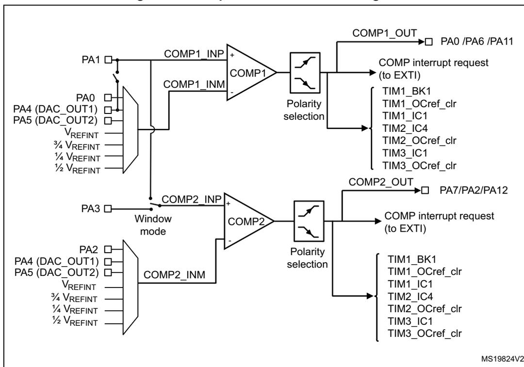
15.3.2 COMP pins and internal signals
The I/Os used as comparators inputs must be configured in analog mode in the GPIOs registers.
The comparator output can be connected to the I/Os using the alternate function channel given in “Alternate function mapping” table in the datasheet.
The output can also be internally redirected to a variety of timer input for the following purposes:
- • Emergency shut-down of PWM signals, using BKIN
- • Cycle-by-cycle current control, using OCREF_CLR inputs
- • Input capture for timing measures
It is possible to have the comparator output simultaneously redirected internally and externally.
15.3.3 COMP reset and clocks
The COMP clock provided by the clock controller is synchronous with the PCLK (APB clock).
There is no clock enable control bit provided in the RCC controller. Reset and clock enable bits are common for COMP and SYSCFG.
Important: The polarity selection logic and the output redirection to the port works independently from the PCLK clock. This allows the comparator to work even in Stop mode.
15.3.4 Comparator LOCK mechanism
The comparators can be used for safety purposes, such as over-current or thermal protection. For applications having specific functional safety requirements, it is necessary to insure that the comparator programming cannot be altered in case of spurious register access or program counter corruption.
For this purpose, the comparator control and status registers can be write-protected (read-only).
Once the programming is completed, using bits 30:16 and 15:0 of COMP_CSR, the COMPx LOCK bit can be set to 1. This causes the whole COMP_CSR register to become read-only, including the COMPx LOCK bit.
The write protection can only be reset by a MCU reset.
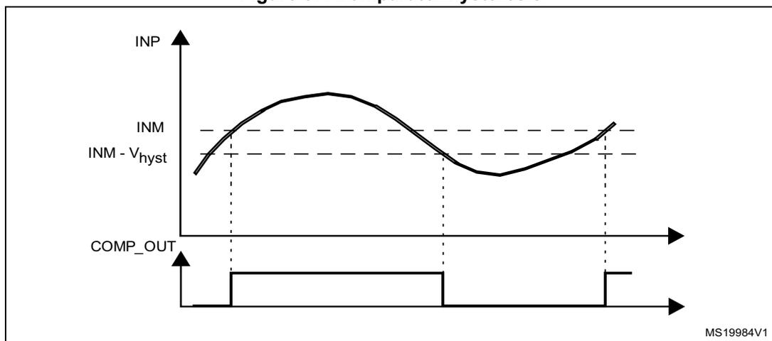
15.3.5 Hysteresis
The comparator includes a programmable hysteresis to avoid spurious output transitions in case of noisy signals. The hysteresis can be disabled if it is not needed (for instance when exiting from low-power mode) to be able to force the hysteresis value using external components.
Figure 57. Comparator hysteresis
15.3.6 Power mode
The comparator power consumption versus propagation delay can be adjusted to have the optimum trade-off for a given application. The bits COMPxMODE[1:0] in COMP_CSR register can be programmed as follows:
- • 00: High speed / full power
- • 01: Medium speed / medium power
- • 10: Low speed / low-power
- • 11: Very-low speed / ultra-low-power
15.4 COMP interrupts
The comparator outputs are internally connected to the Extended interrupts and events controller. Each comparator has its own EXTI line and can generate either interrupts or events. The same mechanism is used to exit from low-power modes.
Refer to Interrupt and events section for more details.
15.5 COMP registers
15.5.1 COMP control and status register (COMP_CSR)
Address offset: 0x1C
Reset value: 0x0000 0000
| 31 | 30 | 29 | 28 | 27 | 26 | 25 | 24 | 23 | 22 | 21 | 20 | 19 | 18 | 17 | 16 |
|---|---|---|---|---|---|---|---|---|---|---|---|---|---|---|---|
| COMP2 LOCK | COMP2 OUT | COMP2HYST [1:0] | COMP2 POL | COMP2OUTSEL[2:0] | WNDW EN | COMP2INSEL[2:0] | COMP2MODE [1:0] | Res. | COMP2 EN | ||||||
| rwo | r | rw/r | rw/r | rw/r | rw/r | rw/r | rw/r | rw/r | rw/r | rw/r | rw/r | rw/r | rw/r | rw/r | |
| 15 | 14 | 13 | 12 | 11 | 10 | 9 | 8 | 7 | 6 | 5 | 4 | 3 | 2 | 1 | 0 |
|---|---|---|---|---|---|---|---|---|---|---|---|---|---|---|---|
| COMP1 LOCK | COMP1 OUT | COMP1HYST [1:0] | COMP1 POL | COMP1OUTSEL[2:0] | Res. | COMP1INSEL[2:0] | COMP1MODE [1:0] | COMP1 SW1 | COMP1 EN | ||||||
| rwo | r | rw/r | rw/r | rw/r | rw/r | rw/r | rw/r | rw/r | rw/r | rw/r | rw/r | rw/r | rw/r | rw/r | |
This bit is write-once. It is set by software. It can only be cleared by a system reset.
It allows to have all control bits of comparator 2 as read-only.
0: COMP_CSR[31:16] bits are read-write.
1: COMP_CSR[31:16] bits are read-only.
Bit 30 COMP2OUT : Comparator 2 outputThis read-only bit is a copy of comparator 2 output state.
0: Output is low (non-inverting input below inverting input).
1: Output is high (non-inverting input above inverting input).
Bits 29:28 COMP2HYST[1:0] Comparator 2 hysteresisThese bits control the hysteresis level.
00: No hysteresis
01: Low hysteresis
10: Medium hysteresis
11: High hysteresis
Please refer to the electrical characteristics for the hysteresis values.
Bit 27 COMP2POL : Comparator 2 output polarityThis bit is used to invert the comparator 2 output.
0: Output is not inverted
1: Output is inverted
Bits 26:24 COMP2OUTSEL[2:0] : Comparator 2 output selectionThese bits select the destination of the comparator output.
000: No selection
001: Timer 1 break input
010: Timer 1 Input capture 1
011: Timer 1 OCrefclear input
100: Timer 2 input capture 4
101: Timer 2 OCrefclear input
110: Timer 3 input capture 1
111: Timer 3 OCrefclear input
Bit 23 WNDWEN : Window mode enableThis bit connects the non-inverting input of COMP2 to COMP1's non-inverting input, which is simultaneously disconnected from PA3.
0: Window mode disabled
1: Window mode enabled
Bits 22:20 COMP2INSEL[2:0] : Comparator 2 inverting input selectionThese bits allows to select the source connected to the inverting input of the comparator 2.
000: 1/4 of V REFINT
001: 1/2 of V REFINT
010: 3/4 of V REFINT
011: V REFINT
100: COMP2_INM4 (PA4 with DAC_OUT1 if enabled)
101: COMP2_INM5 (PA5 with DAC_OUT2 if present and enabled)
110: COMP2_INM6 (PA2)
111: Reserved
Bits 19:18 COMP2MODE[1:0] : Comparator 2 mode
These bits control the operating mode of the comparator 2 and allows to adjust the speed/consumption.
- 00: High speed / full power
- 01: Medium speed / medium power
- 10: Low speed / low-power
- 11: Very-low speed / ultra-low power
Bit 17 Reserved, must be kept at reset value.
Bit 16 COMP2EN : Comparator 2 enable
This bit switches ON/OFF the comparator2.
- 0: Comparator 2 disabled
- 1: Comparator 2 enabled
Bit 15 COMP1LOCK : Comparator 1 lock
This bit is write-once. It is set by software. It can only be cleared by a system reset.
It allows to have all control bits of comparator 1 as read-only.
- 0: COMP_CSR[15:0] bits are read-write.
- 1: COMP_CSR[15:0] bits are read-only.
Bit 14 COMP1OUT : Comparator 1 output
This read-only bit is a copy of comparator 1 output state.
- 0: Output is low (non-inverting input below inverting input).
- 1: Output is high (non-inverting input above inverting input).
Bits 13:12 COMP1HYST[1:0] Comparator 1 hysteresis
These bits are controlling the hysteresis level.
- 00: No hysteresis
- 01: Low hysteresis
- 10: Medium hysteresis
- 11: High hysteresis
Please refer to the electrical characteristics for the hysteresis values.
Bit 11 COMP1POL : Comparator 1 output polarity
This bit is used to invert the comparator 1 output.
- 0: output is not inverted
- 1: output is inverted
Bits 10:8 COMP1OUTSEL[2:0] : Comparator 1 output selection
These bits selects the destination of the comparator 1 output.
- 000: no selection
- 001: Timer 1 break input
- 010: Timer 1 Input capture 1
- 011: Timer 1 OCrefclear input
- 100: Timer 2 input capture 4
- 101: Timer 2 OCrefclear input
- 110: Timer 3 input capture 1
- 111: Timer 3 OCrefclear input
Bit 7 Reserved, must be kept at reset value.
Bits 6:4 COMP1INSEL[2:0] : Comparator 1 inverting input selection
These bits select the source connected to the inverting input of the comparator 1.
- 000: 1/4 of V REFINT
- 001: 1/2 of V REFINT
- 010: 3/4 of V REFINT
- 011: V REFINT
- 100: COMP1_INM4 (PA4 with DAC_OUT1 if enabled)
- 101: COMP1_INM5 (PA5 with DAC_OUT2 if present and enabled)
- 110: COMP1_INM6 (PA0)
- 111: Reserved
Bits 3:2 COMP1MODE[1:0] : Comparator 1 mode
These bits control the operating mode of the comparator 1 and allows to adjust the speed/consumption.
- 00: High speed / full power
- 01: Medium speed / medium power
- 10: Low speed / low-power
- 11: Very-low speed / ultra-low power
Bit 1 COMP1SW1 : Comparator 1 non inverting input DAC switch
This bit closes a switch between comparator 1 non-inverting input on PA1 and PA4 (DAC) I/O.
- 0: Switch open
- 1: Switch closed
Note: This switch is solely intended to redirect signals onto high impedance input, such as COMP1 non-inverting input (highly resistive switch).
Bit 0 COMP1EN : Comparator 1 enable
This bit switches COMP1 ON/OFF.
- 0: Comparator 1 disabled
- 1: Comparator 1 enabled
15.5.2 COMP register map
The following table summarizes the comparator registers.
Table 54. COMP register map and reset values
| Offset | Register | 31 | 30 | 29 | 28 | 27 | 26 | 25 | 24 | 23 | 22 | 21 | 20 | 19 | 18 | 17 | 16 | 15 | 14 | 13 | 12 | 11 | 10 | 9 | 8 | 7 | 6 | 5 | 4 | 3 | 2 | 1 | 0 |
|---|---|---|---|---|---|---|---|---|---|---|---|---|---|---|---|---|---|---|---|---|---|---|---|---|---|---|---|---|---|---|---|---|---|
| 0x1C | COMP_CSR | COMP2LOCK | COMP2OUT | COMP2HYST1:0 | COMP2POL | COMP2OUTSEL[2:0] | WNDWEN | COMP2INSEL[2:0] | COMP2MODE1:0 | COMP2EN | COMP1LOCK | COMP1OUT | COMP1HYST1:0 | COMP1POL | COMP1OUTSEL[2:0] | COMP1INSEL[2:0] | COMP1MODE1:0 | COMP1SW1 | COMP1EN | ||||||||||||||
| Reset value | 0 | 0 | 0 | 0 | 0 | 0 | 0 | 0 | 0 | 0 | 0 | 0 | 0 | 0 | 0 | 0 | 0 | 0 | 0 | 0 | 0 | 0 | 0 | 0 | 0 | 0 | 0 | 0 | 0 | 0 |
Refer to Section 2.2 on page 46 for the register boundary addresses.