3. Embedded flash memory
3.1 Flash main features
- • Up to 256 Kbyte of flash memory
- • Memory organization:
- – Main flash memory block:
Up to 64 Kword (64 K × 32 bits) - – Information block:
Up to 3 Kword (3 K × 32 bits) for the system memory - – Up to 2 x 8 byte for the option byte
- – Main flash memory block:
Flash memory interface features:
- • Read interface with prefetch buffer
- • Option byte loader
- • Flash program / erase operation
- • Read / write protection
- • Low-power mode
3.2 Flash memory functional description
3.2.1 Flash memory organization
The flash memory is organized as 32-bit wide memory cells that can be used for storing both code and data constants.
The memory organization of STM32F03x, STM32F04x and STM32F05x devices is based on a main flash memory block containing up to 64 pages of 1 Kbyte or up to 16 sectors of 4 Kbytes (4 pages). The sector is the granularity of the write protection (see Section 3.3 ).
The memory organization of STM32F07x and STM32F09x devices is based on a main flash memory block containing up to 128 pages of 2 Kbytes or up to 64 sectors of 4 Kbytes (2 pages). The sector is the granularity of the write protection (see Section 3.3 ).
The information block is divided into two parts:
- 1. System memory: used to boot the device in System memory boot mode. The area is reserved for use by STMicroelectronics and contains the boot loader, which is used to reprogram the flash memory through the selected communication interface. It is programmed by ST when the device is manufactured, and protected against spurious write/erase operations. For further details refer to AN2606.
- 2. Option byte
Table 4. Flash memory organization (STM32F03x, STM32F04x and STM32F05x devices)
| Flash area | Flash memory addresses | Size (byte) | Name | Description |
|---|---|---|---|---|
| Main flash memory | 0x0800 0000 - 0x0800 03FF | 1 Kbyte | Page 0 | Sector 0 |
| 0x0800 0400 - 0x0800 07FF | 1 Kbyte | Page 1 | ||
| 0x0800 0800 - 0x0800 0BFF | 1 Kbyte | Page 2 | ||
| 0x0800 0C00 - 0x0800 0FFF | 1 Kbyte | Page 3 | ||
| . | . | . | . | |
| . | . | . | . | |
| . | . | . | . | |
| 0x0800 7000 - 0x0800 73FF | 1 Kbyte | Page 28 | Sector 7 (1) | |
| 0x0800 7400 - 0x0800 77FF | 1 Kbyte | Page 29 | ||
| 0x0800 7800 - 0x0800 7BFF | 1 Kbyte | Page 30 | ||
| 0x0800 7C00 - 0x0800 7FFF | 1 Kbyte | Page 31 | ||
| . | . | . | . | |
| . | . | . | . | |
| . | . | . | . | |
| 0x0800 F000 - 0x0800 F3FF | 1 Kbyte | Page 60 | Sector 15 | |
| 0x0800 F400 - 0x0800 F7FF | 1 Kbyte | Page 61 | ||
| 0x0800 F800 - 0x0800 FBFF | 1 Kbyte | Page 62 | ||
| 0x0800 FC00 - 0x0800 FFFF | 1 Kbyte | Page 63 | ||
| Information block | 0x1FFF EC00 - 0x1FFF F7FF | 3 Kbyte (2) | - | System memory |
| 0x1FFF C400 - 0x1FFF F7FF | 13 Kbyte (3) | - | System memory | |
| 0x1FFF F800 - 0x1FFF F80F | 2 x 8 byte | - | Option byte |
1. Main flash memory space of STM32F03x and STM32F04x devices is limited to sector 7.
2. STM32F03x and STM32F05x devices.
3. STM32F04x devices.
Table 5. Flash memory organization (STM32F07x, STM32F09x devices)
| Flash area | Flash memory addresses | Size (byte) | Name | Description |
|---|---|---|---|---|
| Main flash memory | 0x0800 0000 - 0x0800 07FF | 2 Kbytes | Page 0 | Sector 0 |
| 0x0800 0800 - 0x0800 0FFF | 2 Kbytes | Page 1 | ||
| . | . | . | . | |
| . | . | . | . | |
| . | . | . | . | |
| 0x0801 F000 - 0x0801 F7FF | 2 Kbytes | Page 62 | Sector 31 (1) | |
| 0x0801 F800 - 0x0801 FFFF | 2 Kbytes | Page 63 | ||
| . | . | . | . | |
| Information block | 0x0803 F000 - 0x0803 F7FF | 2 Kbytes | Page 126 | - |
| 0x0803 F800 - 0x0803 FFFF | 2 Kbytes | Page 127 | - | |
| 0x1FFF C800 - 0x1FFF F7FF | 12 Kbytes (2) | - | System memory | |
| 0x1FFF D800 - 0x1FFF F7FF | 8 Kbytes (3) | - | System memory | |
| 0x1FFF F800 - 0x1FFF F80F | 2 x 8 byte | - | Option byte |
1. The main flash memory space of STM32F07x is limited to sector 31.
2. STM32F07x devices only.
3. STM32F09x devices only.
Read operations
The embedded flash module can be addressed directly, as a common memory space. Any data read operation accesses the content of the flash module through dedicated read senses and provides the requested data.
The instruction fetch and the data access are both done through the same AHB bus. Read accesses can be performed with the following options managed through the flash access control register (FLASH_ACR):
- • Instruction fetch: Prefetch buffer enabled for a faster CPU execution
- • Latency: number of wait states for a correct read operation (from 0 to 1)
Instruction fetch
The Cortex ® -M0 fetches the instruction over the AHB bus. The prefetch block aims at increasing the efficiency of instruction fetching.
Prefetch buffer
The prefetch buffer is 3-block wide where each block consists of 4 bytes. The prefetch blocks are direct-mapped. A block can be completely replaced on a single read to the flash memory as the size of the block matches the bandwidth of the flash memory.
The implementation of this prefetch buffer makes a faster CPU execution possible as the CPU fetches one word at a time with the next word readily available in the prefetch buffer. This implies that the acceleration ratio is of the order of 2, assuming that the code is aligned at a 32-bit boundary for the jumps.
However the prefetch buffer has an impact on the performance only when the wait state number is 1. In the other case (no wait state) the performance remains the same whatever the prefetch buffer status. There could be some impacts on the power consumption but this is strongly dependent from the actual application code.
Prefetch controller
The prefetch controller decides to access the flash memory depending on the available space in the prefetch buffer. The Controller initiates a read request when there is at least one block free in the prefetch buffer.
The prefetch buffer is usually switched on/off during the initialization routine, while the microcontroller is running on the internal 8 MHz RC (HSI) oscillator.
Access latency
In order to maintain the control signals to read the flash memory, the ratio of the prefetch controller clock period to the access time of the flash memory has to be programmed in the flash access control register with the LATENCY[2:0] bits. This value gives the number of cycles needed to maintain the control signals of the flash memory and correctly read the required data. After reset, the value is zero and only one cycle without additional wait states is required to access the flash memory.
3.2.2 Flash program and erase operations
The STM32F0xx embedded flash memory can be programmed using in-circuit programming or in-application programming.
The in-circuit programming (ICP) method is used to update the entire contents of the flash memory, using the SWD protocol or the boot loader to load the user application into the microcontroller. ICP offers quick and efficient design iterations and eliminates unnecessary package handling or socketing of devices.
In contrast to the ICP method, in-application programming (IAP) can use any communication interface supported by the microcontroller (I/Os, USB, CAN, USART, I 2 C, SPI, etc.) to download programming data into memory. IAP allows the user to re-program the flash memory while the application is running. Nevertheless, part of the application has to have been previously programmed in the flash memory using ICP.
The program and erase operations can be performed over the whole product voltage range. They are managed through the following seven flash registers:
- • Key register (FLASH_KEYR)
- • Option byte key register (FLASH_OPTKEYR)
- • Flash control register (FLASH_CR)
- • Flash status register (FLASH_SR)
- • Flash address register (FLASH_AR)
- • Option byte register (FLASH_OBR)
- • Write protection register (FLASH_WRPR)
An ongoing flash memory operation does not block the CPU as long as the CPU does not access the flash memory.
On the contrary, during a program/erase operation to the flash memory, any attempt to read the flash memory stalls the bus. The read operation proceeds correctly once the
program/erase operation has completed. This means that code or data fetches cannot be made while a program/erase operation is ongoing.
For program and erase operations on the flash memory (write/erase), the internal RC oscillator (HSI) must be ON.
Unlocking the flash memory
After reset, the flash memory is protected against unwanted write or erase operations. The FLASH_CR register is not accessible in write mode, except for the OBL_LAUNCH bit, used to reload the option bits. An unlocking sequence should be written to the FLASH_KEYR register to open the access to the FLASH_CR register. This sequence consists of two write operations:
- • Write KEY1 = 0x45670123
- • Write KEY2 = 0xCDEF89AB
Any wrong sequence locks up the FLASH_CR register until the next reset.
In the case of a wrong key sequence, a bus error is detected and a Hard Fault interrupt is generated. This is done after the first write cycle if KEY1 does not match, or during the second write cycle if KEY1 has been correctly written but KEY2 does not match.
The FLASH_CR register can be locked again by user software by writing the LOCK bit in the FLASH_CR register to 1.
For code example refer to the Appendix section A.2.1: Flash memory unlocking sequence .
Main flash memory programming
The main flash memory can be programmed 16 bits at a time. The program operation is started when the CPU writes a half-word into a main flash memory address with the PG bit of the FLASH_CR register set. Any attempt to write data that are not half-word long results in a bus error generating a Hard Fault interrupt.
Figure 3. Programming procedure
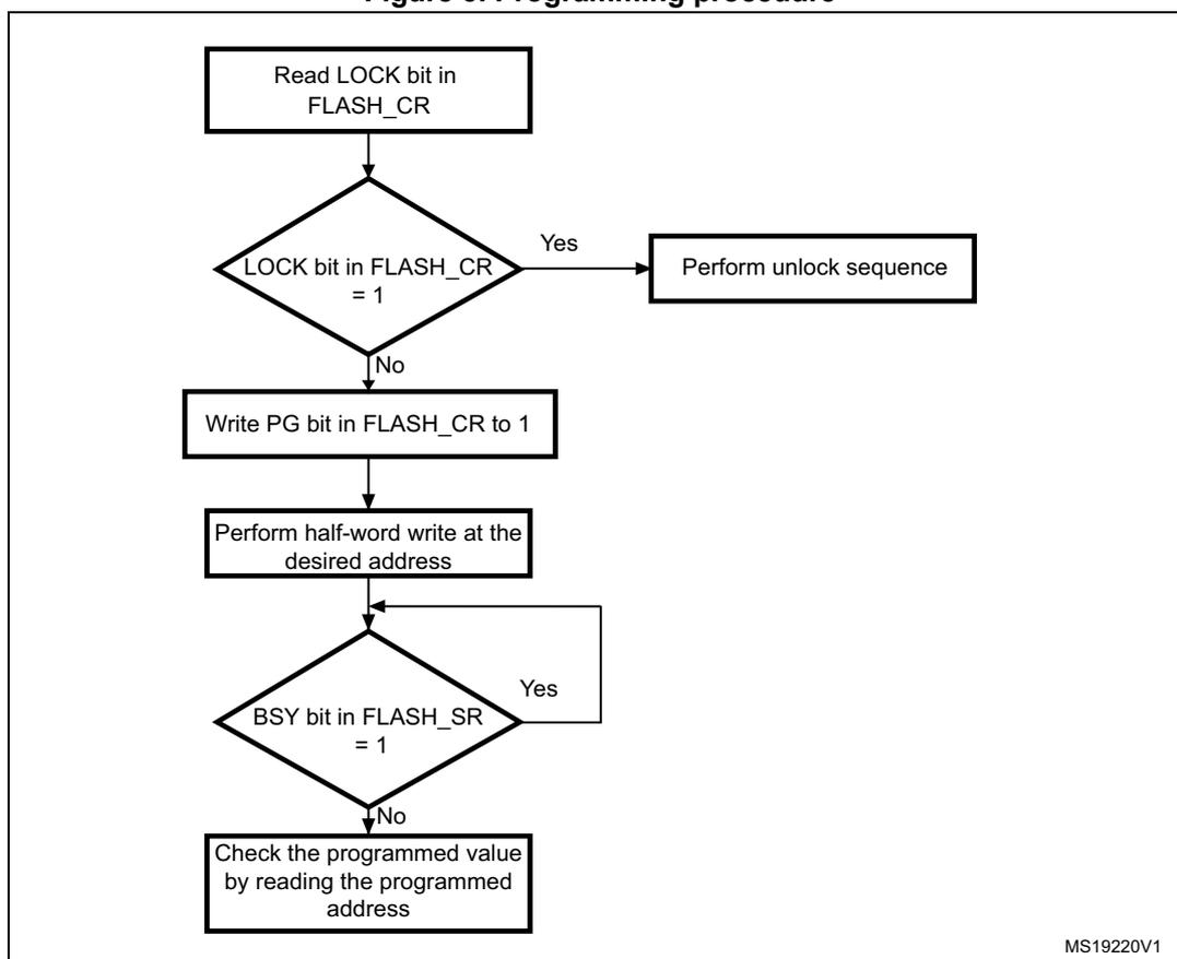
graph TD; A[Read LOCK bit in FLASH_CR] --> B{LOCK bit in FLASH_CR = 1}; B -- Yes --> C[Perform unlock sequence]; B -- No --> D[Write PG bit in FLASH_CR to 1]; D --> E[Perform half-word write at the desired address]; E --> F{BSY bit in FLASH_SR = 1}; F -- Yes --> F; F -- No --> G[Check the programmed value by reading the programmed address];The flowchart illustrates the programming procedure for embedded flash memory. It begins with reading the LOCK bit in the FLASH_CR register. If the LOCK bit is set to 1, an unlock sequence must be performed. If the LOCK bit is not set to 1, the PG bit in the FLASH_CR register is written to 1. This is followed by a half-word write at the desired address. The process then enters a loop waiting for the BSY bit in the FLASH_SR register to be cleared (set to 0). Once the BSY bit is 0, the programmed value is checked by reading the programmed address.
MS19220V1
The flash memory interface preliminarily reads the value at the addressed main flash memory location and checks that it has been erased. If not, the program operation is skipped and a warning is issued by the PGERR bit in FLASH_SR register. The only exception to this is when 0x0000 is programmed. In this case, the location is correctly programmed to 0x0000 and the PGERR bit is not set.
If the addressed main flash memory location is write-protected by the FLASH_WRP register, the program operation is skipped and a warning is issued by the WRPRTERR bit in the FLASH_SR register. The end of the program operation is indicated by the EOP bit in the FLASH_SR register.
The main flash memory programming sequence in standard mode is as follows:
- 1. Check that no main flash memory operation is ongoing by checking the BSY bit in the FLASH_SR register.
- 2. Set the PG bit in the FLASH_CR register.
- 3. Perform the data write (half-word) at the desired address.
- 4. Wait until the BSY bit is reset in the FLASH_SR register.
- 5. Check the EOP flag in the FLASH_SR register (it is set when the programming operation has succeeded), and then clear it by software.
Note: The registers are not accessible in write mode when the BSY bit of the FLASH_SR register is set.
For code example refer to the Appendix section A.2.2: Main Flash programming sequence .
Flash memory erase
The flash memory can be erased page by page or completely (mass erase).
Page erase
To erase a page, the procedure below should be followed:
- 1. Check that no flash memory operation is ongoing by checking the BSY bit in the FLASH_SR register.
- 2. Set the PER bit in the FLASH_CR register.
- 3. Program the FLASH_AR register to select a page to erase.
- 4. Set the STRT bit in the FLASH_CR register (see note below).
- 5. Wait for the BSY bit to be reset.
- 6. Check the EOP flag in the FLASH_SR register (it is set when the erase operation has succeeded).
- 7. Clear the EOP flag.
Note: The software should start checking if the BSY bit equals “0” at least one CPU cycle after setting the STRT bit.
For code example refer to the Appendix section A.2.3: Page erase sequence .
Figure 4. Flash memory Page erase procedure
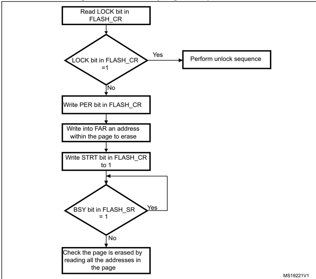
graph TD; A[Read LOCK bit in FLASH_CR] --> B{LOCK bit in FLASH_CR = 1}; B -- Yes --> C[Perform unlock sequence]; B -- No --> D[Write PER bit in FLASH_CR]; D --> E[Write into FAR an address within the page to erase]; E --> F[Write STRT bit in FLASH_CR to 1]; F --> G{BSY bit in FLASH_SR = 1}; G -- Yes --> F; G -- No --> H[Check the page is erased by reading all the addresses in the page];MS19221V1
Mass erase
The mass erase command can be used to completely erase the pages of the main flash memory. The information block is unaffected by this procedure. The following sequence is recommended:
- 1. Check that no flash memory operation is ongoing by checking the BSY bit in the FLASH_SR register.
- 2. Set the MER bit in the FLASH_CR register.
- 3. Set the STRT bit in the FLASH_CR register.
- 4. Wait until the BSY bit is reset in the FLASH_SR register.
- 5. Check the EOP flag in the FLASH_SR register (it is set when the programming operation has succeeded).
- 6. Clear the EOP flag.
Note: The software should start checking if the BSY bit equals “0” at least one CPU cycle after setting the STRT bit.
For code example refer to the Appendix section A.2.4: Mass erase sequence .
Figure 5. Flash memory mass erase procedure
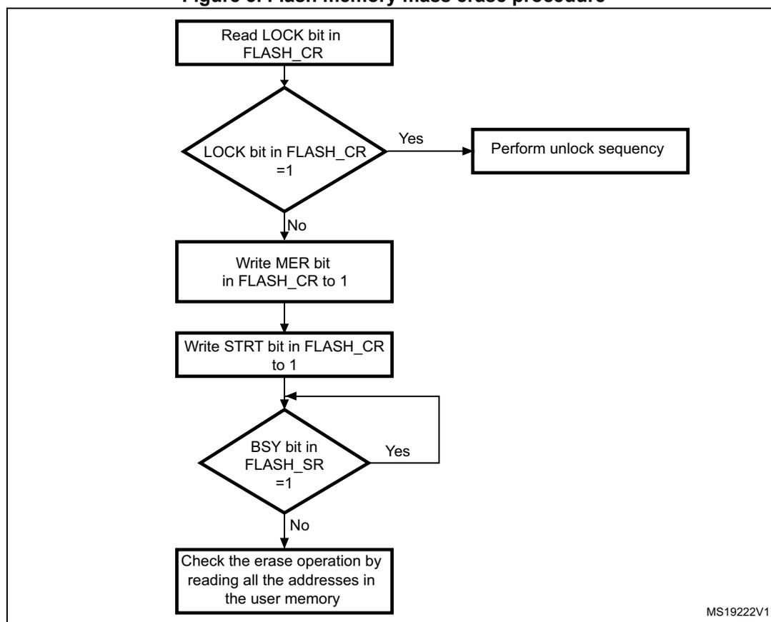
graph TD; A[Read LOCK bit in FLASH_CR] --> B{LOCK bit in FLASH_CR = 1}; B -- Yes --> C[Perform unlock sequence]; B -- No --> D[Write MER bit in FLASH_CR to 1]; D --> E[Write STRT bit in FLASH_CR to 1]; E --> F{BSY bit in FLASH_SR = 1}; F -- Yes --> F; F -- No --> G[Check the erase operation by reading all the addresses in the user memory];The flowchart illustrates the mass erase procedure. It begins with reading the LOCK bit in the FLASH_CR register. If the LOCK bit is 1, an unlock sequence must be performed. If the LOCK bit is not 1, the MER bit in the FLASH_CR register is set to 1, followed by setting the STRT bit in the FLASH_CR register to 1. After these steps, the BSY bit in the FLASH_SR register is checked. If the BSY bit is 1, the process loops back to the check. If the BSY bit is not 1, the erase operation is checked by reading all the addresses in the user memory.
MS19222V1
Option byte programming
The option byte are programmed differently from normal user addresses. The number of option byte is limited to 8 (1, 2 or 4 for write protection, 1 for read protection, 1 for hardware configuration and 2 free byte for user data). After unlocking the flash access, the user has to authorize the programming of the option byte by writing the same set of KEYS (KEY1 and KEY2) to the FLASH_OPTKEYR register to set the OPTWRE bit in the FLASH_CR register (refer to Unlocking the flash memory for key values). Then the user has to set the OPTPG bit in the FLASH_CR register and perform a half-word write operation at the desired flash address.
The value of the addressed option byte is first read to check it is really erased. If not, the program operation is skipped and a warning is issued by the WRPRTERR bit in the FLASH_SR register. The end of the program operation is indicated by the EOP bit in the FLASH_SR register.
The option byte is automatically complemented into the next flash memory address before the programming operation starts. This guarantees that the option byte and its complement are always correct.
The sequence is as follows:
- 1. Check that no flash memory operation is ongoing by checking the BSY bit in the FLASH_SR register.
- 2. Unlock the OPTWRE bit in the FLASH_CR register.
- 3. Set the OPTPG bit in the FLASH_CR register.
- 4. Write the data (half-word) to the desired address.
- 5. Wait for the BSY bit to be reset.
- 6. Read the programmed value and verify.
For code example refer to the Appendix section A.2.6: Option byte programming sequence .
When the flash memory read protection option is changed from protected to unprotected, a mass erase of the main flash memory is performed before reprogramming the read protection option. If the user wants to change an option other than the read protection option, then the mass erase is not performed. The erased state of the read protection option byte protects the flash memory.
Erase procedure
The option byte erase sequence is as follows:
- 1. Check that no flash memory operation is ongoing by reading the BSY bit in the FLASH_SR register
- 2. Unlock the OPTWRE bit in the FLASH_CR register
- 3. Set the OPTER bit in the FLASH_CR register
- 4. Set the STRT bit in the FLASH_CR register
- 5. Wait for the BSY bit to be reset
- 6. Read the erased option byte and verify
For code example refer to the Appendix section A.2.7: Option byte erasing sequence .
3.3 Memory protection
The user area of the flash memory can be protected against read by untrusted code. The pages of the flash memory can also be protected against unwanted write due to loss of program counter contexts. The write-protection granularity is one sector (four pages).
3.3.1 Read protection
The read protection is activated by setting the RDP option byte and then, by applying a system reset to reload the new RDP option byte.
Note: If the read protection is set while the debugger is still connected through SWD, apply a POR (power-on reset) instead of a system reset.
There are three levels of read protection from no protection (level 0) to maximum protection or no debug (level 2). Refer to Table 7: Access status versus protection level and execution modes .
The flash memory is protected when the RDP option byte and its complement contain the pair of values shown in Table 6 .
Table 6. Flash memory read protection status
| RDP byte value | RDP complement value | Read protection level |
|---|---|---|
| 0xAA | 0x55 | Level 0 (ST production configuration) |
| Any value except 0xAA or 0xCC | Any value (not necessarily complementary) except 0x55 and 0x33 | Level 1 |
| 0xCC | 0x33 | Level 2 |
The System memory area is read accessible whatever the protection level. It is never accessible for program/erase operation
Level 0: no protection
Read, program and erase operations into the main flash memory area are possible.
The option byte are as well accessible by all operations.
Level 1: read protection
This is the default protection level when RDP option byte is erased. It is defined as well when RDP value is at any value different from 0xAA and 0xCC, or even if the complement is not correct.
- • User mode: Code executing in user mode can access main flash memory and option byte with all operations.
- • Debug, boot RAM and boot loader modes: In debug mode (with SWD) or when code is running from boot RAM or boot loader, the main flash memory and the backup registers (RTC_BKPxR in the RTC) are totally inaccessible. In these modes, even a simple read access generates a bus error and a Hard Fault interrupt. The main flash memory is program/erase protected to prevent malicious or unauthorized users from reprogramming any of the user code with a dump routine. Any
attempted program/erase operation sets the PGERR flag of flash status register (FLASH_SR).
When the RPD is reprogrammed to the value 0xAA to move back to Level 0, a mass erase of the main flash memory is performed and the backup registers (RTC_BKPxR in the RTC) are reset.
Level 2: no debug
In this level, the protection level 1 is guaranteed. In addition, the CortexM0 debug capabilities are disabled. Consequently, the debug port (SWD), the boot from RAM (boot RAM mode) and the boot from System memory (boot loader mode) are no more available.
In user execution mode, all operations are allowed on the main flash memory. On the contrary, only read and program operations can be performed on the option byte. Option byte are not accessible for erase operations.
Moreover, the RDP byte cannot be programmed. Thus, the level 2 cannot be removed at all: it is an irreversible operation. When attempting to program the RDP byte, the protection error flag WRPRERR is set in the flash_SR register and an interrupt can be generated.
Note: The debug feature is also disabled under reset.
STMicroelectronics is not able to perform analysis on defective parts on which the level 2 protection has been set.
Table 7. Access status versus protection level and execution modes
| Area | Protection level | User execution | Debug / Boot from RAM / Boot from System memory | ||||
|---|---|---|---|---|---|---|---|
| Read | Write | Erase | Read | Write | Erase | ||
| Main flash memory | 1 | Yes | Yes | Yes | No | No | No (4) |
| 2 | Yes | Yes | Yes | N/A (1) | N/A (1) | N/A (1) | |
| System memory (2) | 1 | Yes (3) | No | No | Yes | No | No |
| 2 | Yes (3) | No | No | N/A (1) | N/A (1) | N/A (1) | |
| Option byte | 1 | Yes | Yes (4) | Yes | Yes (5) | Yes (4)(5) | Yes |
| 2 | Yes | Yes (6) | No | N/A (1) | N/A (1) | N/A (1) | |
| Backup registers (7) | 1 | Yes | Yes | N/A | No | No | No |
| 2 | Yes | Yes | N/A | N/A (1) | N/A (1) | N/A (1) | |
- 1. When the protection level 2 is active, the Debug port, the boot from RAM and the boot from System memory are disabled.
- 2. The system memory is only read-accessible, whatever the protection level (0, 1 or 2) and execution mode.
- 3. Under RDP level 1 and level 2, the bootloader can be accessed by a jump to it. However it does not execute any command other than GetCmd/GetID/GetVersion.
- 4. The main flash memory is erased when the RDP option byte is changed from level 1 to level 0 (0xAA).
- 5. When the RDP level 1 is active, the embedded boot loader does not allow to read or write the Option byte, except to remove the RDP protection (move from level 1 to level 0).
- 6. All option byte can be programmed, except the RDP byte.
- 7. These registers are reset when moving from RDP level 1 to level 0.
Changing read protection level
It is easy to move from level 0 to level 1 by changing the value of the RDP byte to any value (except 0xCC).
By programming the 0xCC value in the RDP byte, it is possible to go to level 2 either directly from level 0 or from level 1.
On the contrary, the change to level 0 (no protection) is not possible without a main flash memory Mass erase operation. This Mass erase is generated as soon as 0xAA is programmed in the RDP byte.
Note: When the mass erase command is used, the backup registers (RTC_BKPxR in the RTC) are also reset.
To validate the protection level change, the option bytes must be reloaded through the “OBL_LAUNCH” bit in flash control register.
3.3.2 Write protection
The write protection is implemented with a granularity of one sector. It is activated by configuring the WRPx option byte, and then by reloading them by setting the OBL_LAUNCH bit in the FLASH_CR register.
If a program or an erase operation is performed on a protected sector, the flash memory returns a WRPRTERR protection error flag in the flash memory Status Register (FLASH_SR).
Write unprotection
To disable the write protection, two application cases are provided:
- • Case 1: Read protection disabled after the write unprotection:
- – Erase the entire option byte area by using the OPTER bit in the flash memory control register (FLASH_CR).
- – Program the code 0xAA in the RDP byte to unprotect the memory. This operation forces a mass erase of the main flash memory.
- – Set the OBL_LAUNCH bit in the flash control register (FLASH_CR) to reload the option byte (and the new WRP[1:0] byte), and to disable the write protection.
- • Case 2: Read protection maintained active after the write unprotection, useful for in-application programming with a user boot loader:
- – Erase the entire option byte area by using the OPTER bit in the flash memory control register (FLASH_CR).
- – Set the OBL_LAUNCH bit in the flash control register (FLASH_CR) to reload the option byte (and the new WRP[1:0] byte), and to disable the write protection.
3.3.3 Option byte write protection
The option byte are always read-accessible and write-protected by default. To gain write access (Program/Erase) to the option byte, a sequence of keys (same as for lock) has to be written into the OPTKEYR. A correct sequence of keys gives write access to the option byte and this is indicated by OPTWRE in the FLASH_CR register being set. Write access can be disabled by resetting the bit through software.
3.4 Flash interrupts
Table 8. Flash interrupt request
| Interrupt event | Event flag | Enable control bit |
|---|---|---|
| End of operation | EOP | EOPIE |
| Write protection error | WRPRTERR | ERRIE |
| Programming error | PGERR | ERRIE |
3.5 Flash register description
The flash memory registers have to be accessed by 32-bit words (half-word and byte accesses are not allowed).
3.5.1 Flash access control register (FLASH_ACR)
Address offset: 0x00
Reset value: 0x0000 0000
| 31 | 30 | 29 | 28 | 27 | 26 | 25 | 24 | 23 | 22 | 21 | 20 | 19 | 18 | 17 | 16 |
|---|---|---|---|---|---|---|---|---|---|---|---|---|---|---|---|
| Res. | Res. | Res. | Res. | Res. | Res. | Res. | Res. | Res. | Res. | Res. | Res. | Res. | Res. | Res. | Res. |
| 15 | 14 | 13 | 12 | 11 | 10 | 9 | 8 | 7 | 6 | 5 | 4 | 3 | 2 | 1 | 0 |
| Res. | Res. | Res. | Res. | Res. | Res. | Res. | Res. | Res. | Res. | PRFT BS | PRFT BE | Res. | LATENCY[2:0] | ||
| r | rw | rw | rw | rw | |||||||||||
Bits 31:6 Reserved, must be kept at reset value.
Bit 5 PRFTBS : Prefetch buffer status
This bit provides the status of the prefetch buffer.
0: Prefetch buffer is disabled
1: Prefetch buffer is enabled
Note: The prefetch status is set to 1 as soon a first fetch request is done
Bit 4 PRFTBE : Prefetch buffer enable
0: Prefetch is disabled
1: Prefetch is enabled
Bit 3 Reserved, must be kept at reset value.
Bits 2:0 LATENCY[2:0] : Latency
These bits represent the ratio of the SYSCLK (system clock) period to the flash access time.
000: Zero wait state, if SYSCLK ≤ 24 MHz
001: One wait state, if 24 MHz < SYSCLK ≤ 48 MHz
3.5.2 Flash key register (FLASH_KEYR)
Address offset: 0x04
Reset value: 0xXXXX XXXX
All these register bits are write-only and return a 0 when read.
| 31 | 30 | 29 | 28 | 27 | 26 | 25 | 24 | 23 | 22 | 21 | 20 | 19 | 18 | 17 | 16 |
| FKEY[31:16] | |||||||||||||||
| w | w | w | w | w | w | w | w | w | w | w | w | w | w | w | w |
| 15 | 14 | 13 | 12 | 11 | 10 | 9 | 8 | 7 | 6 | 5 | 4 | 3 | 2 | 1 | 0 |
| FKEY[15:0] | |||||||||||||||
| w | w | w | w | w | w | w | w | w | w | w | w | w | w | w | w |
Bits 31:0 FKEY : Flash key
These bits represent the keys to unlock the flash.
3.5.3 Flash option key register (FLASH_OPTKEYR)
Address offset: 0x08
Reset value: 0xXXXX XXXX
All these register bits are write-only and return a 0 when read.
| 31 | 30 | 29 | 28 | 27 | 26 | 25 | 24 | 23 | 22 | 21 | 20 | 19 | 18 | 17 | 16 |
| OPTKEY[31:16] | |||||||||||||||
| w | w | w | w | w | w | w | w | w | w | w | w | w | w | w | w |
| 15 | 14 | 13 | 12 | 11 | 10 | 9 | 8 | 7 | 6 | 5 | 4 | 3 | 2 | 1 | 0 |
| OPTKEY[15:0] | |||||||||||||||
| w | w | w | w | w | w | w | w | w | w | w | w | w | w | w | w |
Bits 31:0 OPTKEY : Option byte key
These bits represent the keys to unlock the OPTWRE.
3.5.4 Flash status register (FLASH_SR)
Address offset: 0x0C
Reset value: 0x0000 0000
| 31 | 30 | 29 | 28 | 27 | 26 | 25 | 24 | 23 | 22 | 21 | 20 | 19 | 18 | 17 | 16 |
|---|---|---|---|---|---|---|---|---|---|---|---|---|---|---|---|
| Res. | Res. | Res. | Res. | Res. | Res. | Res. | Res. | Res. | Res. | Res. | Res. | Res. | Res. | Res. | Res. |
| 15 | 14 | 13 | 12 | 11 | 10 | 9 | 8 | 7 | 6 | 5 | 4 | 3 | 2 | 1 | 0 |
| Res. | Res. | Res. | Res. | Res. | Res. | Res. | Res. | Res. | Res. | EOP | WRPRT ERR | Res. | PG ERR | Res. | BSY |
| rc_w1 | rc_w1 | rc_w1 | r |
Bits 31:6 Reserved, must be kept at reset value.
Bit 5 EOP : End of operation
Set by hardware when a flash operation (programming / erase) is completed.
Reset by writing 1.
Note: EOP is asserted at the end of each successful program or erase operation
Bit 4 WRPRTERR : Write protection error
Set by hardware when programming a write-protected address of the flash memory.
Reset by writing 1.
Bit 3 Reserved, must be kept at reset value.
Bit 2 PGERR : Programming error
Set by hardware when an address to be programmed contains a value different from '0xFFFF' before programming.
Reset by writing 1.
Note: The STRT bit in the FLASH_CR register should be reset before starting a programming operation.
Bit 1 Reserved, must be kept at reset value.
Bit 0 BSY : Busy
This indicates that a flash operation is in progress. This is set on the beginning of a flash operation and reset when the operation finishes or when an error occurs.
3.5.5 Flash control register (FLASH_CR)
Address offset: 0x10
Reset value: 0x0000 0080
| 31 | 30 | 29 | 28 | 27 | 26 | 25 | 24 | 23 | 22 | 21 | 20 | 19 | 18 | 17 | 16 |
|---|---|---|---|---|---|---|---|---|---|---|---|---|---|---|---|
| Res. | Res. | Res. | Res. | Res. | Res. | Res. | Res. | Res. | Res. | Res. | Res. | Res. | Res. | Res. | Res. |
| 15 | 14 | 13 | 12 | 11 | 10 | 9 | 8 | 7 | 6 | 5 | 4 | 3 | 2 | 1 | 0 |
| Res. | Res. | OBL_LAUNCH | EOPIE | Res. | ERRIE | OPTWRE | Res. | LOCK | STRT | OPTER | OPTPG | Res. | MER | PER | PG |
| rw | rw | rw | rw | rw | rw | rw | rw | rw | rw | rw |
Bits 31:14 Reserved, must be kept at reset value.
Bit 13 OBL_LAUNCH : Force option byte loading
When set to 1, this bit forces the option byte reloading. This operation generates a system reset.
0: Inactive
1: Active
Bit 12 EOPIE : End of operation interrupt enable
This bit enables the interrupt generation when the EOP bit in the FLASH_SR register goes to 1.
0: Interrupt generation disabled
1: Interrupt generation enabled
Bit 11 Reserved, must be kept at reset value
Bit 10 ERRIE : Error interrupt enable
This bit enables the interrupt generation on an error when PGERR / WRPRERR are set in the FLASH_SR register.
0: Interrupt generation disabled
1: Interrupt generation enabled
Bit 9 OPTWRE : Option byte write enable
When set, the option byte can be programmed. This bit is set on writing the correct key sequence to the FLASH_OPTKEYR register.
This bit can be reset by software
Bit 8 Reserved, must be kept at reset value.
Bit 7 LOCK : Lock
Write to 1 only. When it is set, it indicates that the flash is locked. This bit is reset by hardware after detecting the unlock sequence.
In the event of unsuccessful unlock operation, this bit remains set until the next reset.
Bit 6 STRT : Start
This bit triggers an ERASE operation when set. This bit is set only by software and reset when the BSY bit is reset.
Bit 5 OPTER : Option byte erase
Option byte erase chosen.
Bit 4 OPTPG : Option byte programming
Option byte programming chosen.
Bit 3 Reserved, must be kept at reset value.
Bit 2 MER : Mass erase
Erase of all user pages chosen.
Bit 1 PER : Page erase
Page erase chosen.
Bit 0 PG : Programming
Flash programming chosen.
3.5.6 Flash address register (FLASH_AR)
Address offset: 0x14
Reset value: 0x0000 0000
This register is updated by hardware with the currently/last used address. For Page erase operations, this should be updated by software to indicate the chosen page.

| 31 | 30 | 29 | 28 | 27 | 26 | 25 | 24 | 23 | 22 | 21 | 20 | 19 | 18 | 17 | 16 |
| FAR[31:16] | |||||||||||||||
| w | w | w | w | w | w | w | w | w | w | w | w | w | w | w | w |
| 15 | 14 | 13 | 12 | 11 | 10 | 9 | 8 | 7 | 6 | 5 | 4 | 3 | 2 | 1 | 0 |
| FAR[15:0] | |||||||||||||||
| w | w | w | w | w | w | w | w | w | w | w | w | w | w | w | w |
Bits 31:0 FAR : Flash address
Chooses the address to program when programming is selected, or a page to erase when Page erase is selected.
Note: Write access to this register is blocked when the BSY bit in the FLASH_SR register is set.
3.5.7 Flash Option byte register (FLASH_OBR)
Address offset 0x1C
Reset value: 0xXXXX XX0X
The reset value of this register depends on the value programmed in the option byte.
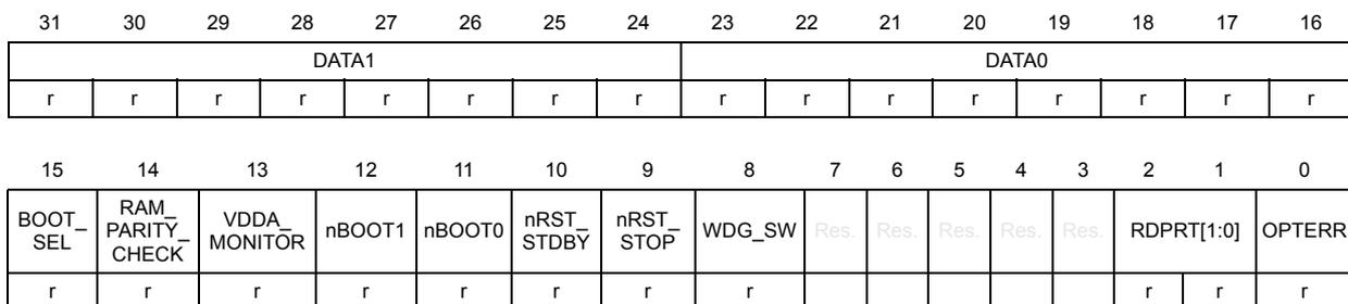
| 31 | 30 | 29 | 28 | 27 | 26 | 25 | 24 | 23 | 22 | 21 | 20 | 19 | 18 | 17 | 16 |
| DATA1 | DATA0 | ||||||||||||||
| r | r | r | r | r | r | r | r | r | r | r | r | r | r | r | r |
| 15 | 14 | 13 | 12 | 11 | 10 | 9 | 8 | 7 | 6 | 5 | 4 | 3 | 2 | 1 | 0 |
| BOOT_SEL | RAM_PARITY_CHECK | VDDA_MONITOR | nBOOT1 | nBOOT0 | nRST_STDBY | nRST_STOP | WDG_SW | Res. | Res. | Res. | Res. | Res. | RDPRT[1:0] | OPTERR | |
| r | r | r | r | r | r | r | r | r | r | r | |||||
Bits 31:24
DATA1
Bits 23:16
DATA0
Bits 15:8 User option bytes:
Bit 15:
BOOT_SEL
(available on STM32F04x and STM32F09x devices only)
Bit 14:
RAM_PARITY_CHECK
Bit 13:
VDDA_MONITOR
Bit 12:
nBOOT1
Bit 11:
nBOOT0
(available on STM32F04x and STM32F09x devices only)
Bit 10:
nRST_STDBY
Bit 9:
nRST_STOP
Bit 8:
WDG_SW
Bits 7:3 Reserved, must be kept at reset value.
Bits 2:1 RDPRT[1:0] : Read protection level status
00: Read protection level 0 is enabled (ST production configuration)
01: Read protection level 1 is enabled
11: Read protection level 2 is enabled.
Bit 0 OPTERR : Option byte error
When set, this indicates that the loaded option byte and its complement do not match. The corresponding byte is set to 0xFF in respective FLASH_OBR or FLASH_WRPR register.
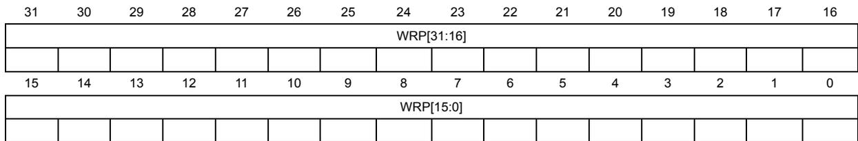
3.5.8 Write protection register (FLASH_WRPR)
Address offset: 0x20
Reset value: 0xXXXX XXXX
The reset value of this register depends on the value programmed in the option byte.
| 31 | 30 | 29 | 28 | 27 | 26 | 25 | 24 | 23 | 22 | 21 | 20 | 19 | 18 | 17 | 16 |
| WRP[31:16] | |||||||||||||||
| 15 | 14 | 13 | 12 | 11 | 10 | 9 | 8 | 7 | 6 | 5 | 4 | 3 | 2 | 1 | 0 |
| WRP[15:0] | |||||||||||||||
Bits 31:0 WRP : Write protect
This register contains the write-protection option byte loaded by the OBL.
3.5.9 Flash register map
Table 9. Flash interface - Register map and reset values
| Off-set | Register | 31 | 30 | 29 | 28 | 27 | 26 | 25 | 24 | 23 | 22 | 21 | 20 | 19 | 18 | 17 | 16 | 15 | 14 | 13 | 12 | 11 | 10 | 9 | 8 | 7 | 6 | 5 | 4 | 3 | 2 | 1 | 0 |
|---|---|---|---|---|---|---|---|---|---|---|---|---|---|---|---|---|---|---|---|---|---|---|---|---|---|---|---|---|---|---|---|---|---|
| 0x000 | FLASH_ACR | Res | Res | Res | Res | Res | Res | Res | Res | Res | Res | Res | Res | Res | Res | Res | Res | Res | Res | Res | Res | Res | Res | Res | Res | Res | Res | PRFTBS | PRFTBE | HIFCYA | LATENCY [2:0] | ||
| Reset value | 0 | 0 | 0 | 0 | 0 | 0 | |||||||||||||||||||||||||||
| 0x004 | FLASH_KEYR | FKEY[31:0] | |||||||||||||||||||||||||||||||
| Reset value | x | x | x | x | x | x | x | x | x | x | x | x | x | x | x | x | x | x | x | x | x | x | x | x | x | x | x | x | x | x | x | ||
| 0x008 | FLASH_OPTKEYR | OPTKEY[31:0] | |||||||||||||||||||||||||||||||
| Reset value | x | x | x | x | x | x | x | x | x | x | x | x | x | x | x | x | x | x | x | x | x | x | x | x | x | x | x | x | x | x | x | ||
| 0x00C | FLASH_SR | Res | Res | Res | Res | Res | Res | Res | Res | Res | Res | Res | Res | Res | Res | Res | Res | Res | Res | Res | Res | Res | Res | Res | Res | Res | Res | EOP | WRPRTERR | Res | PGERR | ERLYBSY | BSY |
| Reset value | 0 | 0 | 0 | 0 | 0 | ||||||||||||||||||||||||||||
| 0x010 | FLASH_CR | Res | Res | Res | Res | Res | Res | Res | Res | Res | Res | Res | Res | Res | Res | Res | Res | Res | Res | OBL_LAUNCH | EOPIE | Res | ERRIE | OPTWRE | Res | LOCK | STRT | OPTER | OPTPG | Res | MER | PER | PG |
| Reset value | 0 | 0 | 0 | 0 | 1 | 0 | 0 | 0 | 0 | 0 | 0 | ||||||||||||||||||||||
| 0x014 | FLASH_AR | FAR[31:0] | |||||||||||||||||||||||||||||||
| Reset value | 0 | 0 | 0 | 0 | 0 | 0 | 0 | 0 | 0 | 0 | 0 | 0 | 0 | 0 | 0 | 0 | 0 | 0 | 0 | 0 | 0 | 0 | 0 | 0 | 0 | 0 | 0 | 0 | 0 | 0 | 0 | 0 | |
| 0x01C | FLASH_OBR | Data1 | Data0 | ||||||||||||||||||||||||||||||
| Reset value | BOOT_SEL | RAM_PARITY_CHECK | VDDA_MONITOR | nBOOT1 | nBOOT0 | nRST_STDBY | nRST_STOP | WDG_SW | Res | Res | Res | Res | RDPRT[1:0] | OPTERR | |||||||||||||||||||
| 0x020 | FLASH_WRPR | WRP[31:0] | |||||||||||||||||||||||||||||||
| Reset value | X | X | X | X | X | X | X | X | X | X | X | X | X | X | X | X | X | X | X | X | X | X | X | X | X | X | X | X | X | X | X | ||