35. USB on-the-go high-speed (OTG_HS)
This section applies to the whole STM32F4xx family, unless otherwise specified.
35.1 OTG_HS introduction
Portions Copyright (c) 2004, 2005 Synopsys, Inc. All rights reserved. Used with permission.
This section presents the architecture and the programming model of the OTG_HS controller.
The following acronyms are used throughout the section:
| FS | full-speed |
| HS | High-speed |
| LS | Low-speed |
| USB | Universal serial bus |
| OTG | On-the-go |
| PHY | Physical layer |
| MAC | Media access controller |
| PFC | Packet FIFO controller |
| UTMI | USB Transceiver Macrocell Interface |
| ULPI | UTMI+ Low Pin Interface |
References are made to the following documents:
- • USB On-The-Go Supplement, Revision 1.3
- • Universal Serial Bus Revision 2.0 Specification
The OTG_HS is a dual-role device (DRD) controller that supports both peripheral and host functions and is fully compliant with the On-The-Go Supplement to the USB 2.0 Specification . It can also be configured as a host-only or peripheral-only controller, fully compliant with the USB 2.0 Specification . In host mode, the OTG_HS supports high-speed (HS, 480 Mbits/s), full-speed (FS, 12 Mbits/s) and low-speed (LS, 1.5 Mbits/s) transfers whereas in peripheral mode, it only supports high-speed (HS, 480Mbits/s) and full-speed (FS, 12 Mbits/s) transfers. The OTG_HS supports both HNP and SRP. The only external device required is a charge pump for VBUS in OTG mode.
35.2 OTG_HS main features
The main features can be divided into three categories: general, host-mode and peripheral-mode features.
35.2.1 General features
The OTG_HS interface main features are the following:
- • It is USB-IF certified in compliance with the Universal Serial Bus Revision 2.0 Specification
- • It supports 3 PHY interfaces
- – An on-chip full-speed PHY
- – An ULPI interface for external high-speed PHY.
- • It supports the host negotiation protocol (HNP) and the session request protocol (SRP)
- • It allows the host to turn \( V_{BUS} \) off to save power in OTG applications, with no need for external components
- • It allows to monitor \( V_{BUS} \) levels using internal comparators
- • It supports dynamic host-peripheral role switching
- • It is software-configurable to operate as:
- – An SRP-capable USB HS/FS peripheral (B-device)
- – An SRP-capable USB HS/FS/low-speed host (A-device)
- – An USB OTG FS dual-role device
- • It supports HS/FS SOFs as well as low-speed (LS) keep-alive tokens with:
- – SOF pulse PAD output capability
- – SOF pulse internal connection to timer 2 (TIM2)
- – Configurable framing period
- – Configurable end-of-frame interrupt
- • It embeds an internal DMA with shareholding support and software selectable AHB burst type in DMA mode
- • It has power saving features such as system clock stop during USB suspend, switching off of the digital core internal clock domains, PHY and DFIFO power management
- • It features a dedicated 4-Kbyte data RAM with advanced FIFO management:
- – The memory partition can be configured into different FIFOs to allow flexible and efficient use of RAM
- – Each FIFO can contain multiple packets
- – Memory allocation is performed dynamically
- – The FIFO size can be configured to values that are not powers of 2 to allow the use of contiguous memory locations
- • It ensures a maximum USB bandwidth of up to one frame without application intervention
35.2.2 Host-mode features
The OTG_HS interface features in host mode are the following:
- • It requires an external charge pump to generate V BUS
- • It has up to 12 host channels (pipes), each channel being dynamically reconfigurable to support any kind of USB transfer
- • It features a built-in hardware scheduler holding:
- – Up to 8 interrupt plus isochronous transfer requests in the periodic hardware queue
- – Up to 8 control plus bulk transfer requests in the nonperiodic hardware queue
- • It manages a shared RX FIFO, a periodic TX FIFO, and a nonperiodic TX FIFO for efficient usage of the USB data RAM
- • It features dynamic trimming capability of SOF framing period in host mode.
35.2.3 Peripheral-mode features
The OTG_HS interface main features in peripheral mode are the following:
- • It has 1 bidirectional control endpoint 0
- • It has 5 IN endpoints (EP) configurable to support bulk, interrupt or isochronous transfers
- • It has 5 OUT endpoints configurable to support bulk, interrupt or isochronous transfers
- • It manages a shared Rx FIFO and a Tx-OUT FIFO for efficient usage of the USB data RAM
- • It manages up to 6 dedicated Tx-IN FIFOs (one for each IN-configured EP) to reduce the application load
- • It features soft disconnect capability
35.3 OTG_HS functional description
Figure 410 shows the OTG_HS interface block diagram.
Figure 410. USB OTG interface block diagram
MSV43325V1
- 1. The USB DMA cannot directly address the internal Flash memory.
35.3.1 OTG pins
Table 207. OTG_HS input/output pins
| Signal name | Signal type | Description |
|---|---|---|
| OTG_HS_DP | Digital input/output | USB OTG D+ line |
| OTG_HS_DM | Digital input/output | USB OTG D- line |
| OTG_HS_ID | Digital input | USB OTG ID |
| OTG_HS_VBUS | Analog input | USB OTG VBUS |
| OTG_HS_SOF | Digital output | USB OTG Start Of Frame (visibility) |
| OTG_HS_ULPI_CK | Digital input | USB OTG ULPI clock |
| OTG_HS_ULPI_DIR | Digital input | USB OTG ULPI data bus direction control |
| OTG_HS_ULPI_STP | Digital output | USB OTG ULPI data stream stop |
| OTG_HS_ULPI_NXT | Digital input | USB OTG ULPI next data stream request |
| OTG_HS_ULPI_D[0..7] | Digital input/output | USB OTG ULPI 8-bit bi-directional data bus |
35.3.2 High-speed OTG PHY
The USB OTG HS core embeds an ULPI interface to connect an external HS phy.
35.3.3 Embedded Full-speed OTG PHY
The full-speed OTG PHY includes the following components:
- • FS/LS transceiver module used by both host and Device. It directly drives transmission and reception on the single-ended USB lines.
- • Integrated ID pull-up resistor used to sample the ID line for A/B Device identification.
- • DP/DM integrated pull-up and pull-down resistors controlled by the OTG_HS core depending on the current role of the device. As a peripheral, it enables the DP pull-up resistor to signal full-speed peripheral connections as soon as \( V_{BUS} \) is sensed to be at a valid level (B-session valid). In host mode, pull-down resistors are enabled on both DP/DM. Pull-up and pull-down resistors are dynamically switched when the peripheral role is changed via the host negotiation protocol (HNP).
- • Pull-up/pull-down resistor ECN circuit
The DP pull-up consists of 2 resistors controlled separately from the OTG_HS as per the resistor Engineering Change Notice applied to USB Rev2.0. The dynamic trimming of the DP pull-up strength allows to achieve a better noise rejection and Tx/Rx signal quality. - • \( V_{BUS} \) sensing comparators with hysteresis used to detect \( V_{BUS\_VALID} \) , A-B Session Valid and session-end voltage thresholds. They are used to drive the session request protocol (SRP), detect valid startup and end-of-session conditions, and constantly monitor the \( V_{BUS} \) supply during USB operations.
- • \( V_{BUS} \) pulsing method circuit used to charge/discharge \( V_{BUS} \) through resistors during the SRP (weak drive).
Caution: To guarantee a correct operation for the USB OTG HS peripheral, the AHB frequency should be higher than 30 MHz.
35.4 OTG dual-role device
35.4.1 ID line detection
The host or peripheral (the default) role depends on the level of the ID input line. It is determined when the USB cable is plugged in and depends on which side of the USB cable is connected to the micro-AB receptacle:
- • If the B-side of the USB cable is connected with a floating ID wire, the integrated pull-up resistor detects a high ID level and the default peripheral role is confirmed. In this configuration the OTG_HS conforms to the FSM standard described in section 6.8.2. On-The-Go B-device of the USB On-The-Go Supplement, Revision 1.3.
- • If the A-side of the USB cable is connected with a grounded ID, the OTG_HS issues an ID line status change interrupt (CIDSCHG bit in the OTG_HS_GINTSTS register) for host software initialization, and automatically switches to host role. In this configuration the OTG_HS conforms to the FSM standard described by section 6.8.1: On-The-Go A-Device of the USB On-The-Go Supplement, Revision 1.3.
35.4.2 HNP dual role device
The HNP capable bit in the Global USB configuration register (HNPCAP bit in the OTG_HS_GUSBCFG register) configures the OTG_HS core to dynamically change from A-host to A-device role and vice-versa, or from B-device to B-host role and vice-versa, according to the host negotiation protocol (HNP). The current device status is defined by the
combination of the Connector ID Status bit in the Global OTG control and status register (CIDSTS bit in OTG_HS_GOTGCTL) and the current mode of operation bit in the global interrupt and status register (CMOD bit in OTG_HS_GINTSTS).
The HNP programming model is described in detail in Section 35.13: OTG_HS programming model .
35.4.3 SRP dual-role device
The SRP capable bit in the global USB configuration register (SRPCAP bit in OTG_HS_GUSBCFG) configures the OTG_HS core to switch \( V_{BUS} \) off for the A-device in order to save power. The A-device is always in charge of driving \( V_{BUS} \) regardless of the OTG_HS role (host or peripheral). The SRP A/B-device program model is described in detail in Section 35.13: OTG_HS programming model .
35.5 USB functional description in peripheral mode
The OTG_HS operates as an USB peripheral in the following circumstances:
- • OTG B-device
OTG B-device default state if the B-side of USB cable is plugged in - • OTG A-device
OTG A-device state after the HNP switches the OTG_HS to peripheral role - • B-Device
If the ID line is present, functional and connected to the B-side of the USB cable, and the HNP-capable bit in the Global USB Configuration register (HNPCAP bit in OTG_HS_GUSBCFG) is cleared (see On-The-Go specification Revision 1.3 section 6.8.3). - • Peripheral only (see
Figure 388: USB peripheral-only connection
)
The force peripheral mode bit in the Global USB configuration register (FDMOD in OTG_HS_GUSBCFG) is set to 1, forcing the OTG_HS core to operate in USB peripheral-only mode (see On-The-Go specification Revision 1.3 section 6.8.3). In this case, the ID line is ignored even if it is available on the USB connector.
Note: To build a bus-powered device architecture in the B-Device or peripheral-only configuration, an external regulator must be added to generate the \( V_{DD} \) supply voltage from \( V_{BUS} \) .
35.5.1 SRP-capable peripheral
The SRP capable bit in the Global USB configuration register (SRPCAP bit in OTG_HS_GUSBCFG) configures the OTG_HS to support the session request protocol (SRP). As a result, it allows the remote A-device to save power by switching \( V_{BUS} \) off when the USB session is suspended.
The SRP peripheral mode program model is described in detail in Section : B-device session request protocol .
35.5.2 Peripheral states
Powered state
The \( V_{BUS} \) input detects the B-session valid voltage used to put the USB peripheral in the Powered state (see USB2.0 specification section 9.1). The OTG_HS then automatically connects the DP pull-up resistor to signal full-speed device connection to the host, and generates the session request interrupt (SRQINT bit in OTG_HS_GINTSTS) to notify the Powered state. The \( V_{BUS} \) input also ensures that valid \( V_{BUS} \) levels are supplied by the host during USB operations. If \( V_{BUS} \) drops below the B-session valid voltage (for example because power disturbances occurred or the host port has been switched off), the OTG_HS automatically disconnects and the session end detected (SEDET bit in OTG_HS_GOTGINT) interrupt is generated to notify that the OTG_HS has exited the Powered state.
In Powered state, the OTG_HS expects a reset from the host. No other USB operations are possible. When a reset is received, the reset detected interrupt (USBRST in OTG_HS_GINTSTS) is generated. When the reset is complete, the enumeration done interrupt (ENUMDNE bit in OTG_HS_GINTSTS) is generated and the OTG_HS enters the Default state.
Soft disconnect
The Powered state can be exited by software by using the soft disconnect feature. The DP pull-up resistor is removed by setting the Soft disconnect bit in the device control register (SDIS bit in OTG_HS_DCTL), thus generating a device disconnect detection interrupt on the host side even though the USB cable was not really unplugged from the host port.
Default state
In Default state the OTG_HS expects to receive a SET_ADDRESS command from the host. No other USB operations are possible. When a valid SET_ADDRESS command is decoded on the USB, the application writes the corresponding number into the device address field in the device configuration register (DAD bit in OTG_HS_DCFG). The OTG_HS then enters the address state and is ready to answer host transactions at the configured USB address.
Suspended state
The OTG_HS peripheral constantly monitors the USB activity. When the USB remains idle for 3 ms, the early suspend interrupt (ESUSP bit in OTG_HS_GINTSTS) is issued. It is confirmed 3 ms later, if appropriate, by generating a suspend interrupt (USBSUSP bit in OTG_HS_GINTSTS). The device suspend bit is then automatically set in the device status register (SUSPSTS bit in OTG_HS_DSTS) and the OTG_HS enters the Suspended state.
The device can also exit from the Suspended state by itself. In this case the application sets the remote wake-up signaling bit in the device control register (RWUSIG bit in OTG_HS_DCTL) and clears it after 1 to 15 ms.
When a resume signaling is detected from the host, the resume interrupt (WKUPINT bit in OTG_HS_GINTSTS) is generated and the device suspend bit is automatically cleared.
35.5.3 Peripheral endpoints
The OTG_HS core instantiates the following USB endpoints:
- • Control endpoint 0
This endpoint is bidirectional and handles control messages only.
It has a separate set of registers to handle IN and OUT transactions, as well as dedicated control (OTG_HS_DIEPCTL0/OTG_HS_DOEPCTL0), transfer configuration (OTG_HS_DIEPTSIZ0/OTG_HS_DOEPTSIZ0), and status-interrupt (OTG_HS_DIEPINTx/OTG_HS_DOEPINT0) registers. The bits available inside the control and transfer size registers slightly differ from other endpoints.
- • 5 IN endpoints
- – They can be configured to support the isochronous, bulk or interrupt transfer type.
- – They feature dedicated control (OTG_HS_DIEPCTLx), transfer configuration (OTG_HS_DIEPTSIZx), and status-interrupt (OTG_HS_DIEPINTx) registers.
- – The Device IN endpoints common interrupt mask register (OTG_HS_DIEPMSK) allows to enable/disable a single endpoint interrupt source on all of the IN endpoints (EP0 included).
- – They support incomplete isochronous IN transfer interrupt (IISOIXFR bit in OTG_HS_GINTSTS). This interrupt is asserted when there is at least one isochronous IN endpoint for which the transfer is not completed in the current frame. This interrupt is asserted along with the end of periodic frame interrupt (OTG_HS_GINTSTS/EOPF).
- • 5 OUT endpoints
- – They can be configured to support the isochronous, bulk or interrupt transfer type.
- – They feature dedicated control (OTG_HS_DOEPCTLx), transfer configuration (OTG_HS_DOEPTSIZx) and status-interrupt (OTG_HS_DOEPINTx) registers.
- – The Device Out endpoints common interrupt mask register (OTG_HS_DOEPMSK) allows to enable/disable a single endpoint interrupt source on all OUT endpoints (EP0 included).
- – They support incomplete isochronous OUT transfer interrupt (INCOMPISOOUT bit in OTG_HS_GINTSTS). This interrupt is asserted when there is at least one isochronous OUT endpoint on which the transfer is not completed in the current frame. This interrupt is asserted along with the end of periodic frame interrupt (OTG_HS_GINTSTS/EOPF).
Endpoint controls
The following endpoint controls are available through the device endpoint-x IN/OUT control register (DIEPCTLx/DOEPCTLx):
- • Endpoint enable/disable
- • Endpoint activation in current configuration
- • Program the USB transfer type (isochronous, bulk, interrupt)
- • Program the supported packet size
- • Program the Tx-FIFO number associated with the IN endpoint
- • Program the expected or transmitted data0/data1 PID (bulk/interrupt only)
- • Program the even/odd frame during which the transaction is received or transmitted (isochronous only)
- • Optionally program the NAK bit to always send a negative acknowledge to the host regardless of the FIFO status
- • Optionally program the STALL bit to always stall host tokens to that endpoint
- • Optionally program the Snoop mode for OUT endpoint where the received data CRC is not checked
Endpoint transfer
The device endpoint-x transfer size registers (DIEPTSIZx/DOPTSIZx) allow the application to program the transfer size parameters and read the transfer status.
The programming operation must be performed before setting the endpoint enable bit in the endpoint control register.
Once the endpoint is enabled, these fields are read-only as the OTG FS core updates them with the current transfer status.
The following transfer parameters can be programmed:
- • Transfer size in bytes
- • Number of packets constituting the overall transfer size.
Endpoint status/interrupt
The device endpoint-x interrupt registers (DIEPINTx/DOEPINTx) indicate the status of an endpoint with respect to USB- and AHB-related events. The application must read these registers when the OUT endpoint interrupt bit or the IN endpoint interrupt bit in the core interrupt register (OEPINT bit in OTG_HS_GINTSTS or IEPINT bit in OTG_HS_GINTSTS, respectively) is set. Before the application can read these registers, it must first read the device all endpoints interrupt register (OTG_HS_DAININT) to get the exact endpoint number for the device endpoint-x interrupt register. The application must clear the appropriate bit in this register to clear the corresponding bits in the DAININT and GINTSTS registers.
The peripheral core provides the following status checks and interrupt generation:
- • Transfer completed interrupt, indicating that data transfer has completed on both the application (AHB) and USB sides
- • Setup stage done (control-out only)
- • Associated transmit FIFO is half or completely empty (in endpoints)
- • NAK acknowledge transmitted to the host (isochronous-in only)
- • IN token received when Tx-FIFO was empty (bulk-in/interrupt-in only)
- • OUT token received when endpoint was not yet enabled
- • Babble error condition detected
- • Endpoint disable by application is effective
- • Endpoint NAK by application is effective (isochronous-in only)
- • More than 3 back-to-back setup packets received (control-out only)
- • Timeout condition detected (control-in only)
- • Isochronous out packet dropped without generating an interrupt
35.6 USB functional description on host mode
This section gives the functional description of the OTG_HS in the USB host mode. The OTG_HS works as a USB host in the following circumstances:
- • OTG A-host
OTG A-device default state when the A-side of the USB cable is plugged in - • OTG B-host
OTG B-device after HNP switching to the host role - • A-device
If the ID line is present, functional and connected to the A-side of the USB cable, and the HNP-capable bit is cleared in the Global USB Configuration register (HNPCAP bit in OTG_HS_GUSBCFG). Integrated pull-down resistors are automatically set on the DP/DM lines. - • Host only (
Figure 389: USB host-only connection
).
The force host mode bit in the global USB configuration register (FHMOD bit in OTG_HS_GUSBCFG) forces the OTG_HS core to operate in USB host-only mode. In this case, the ID line is ignored even if it is available on the USB connector. Integrated pull-down resistors are automatically set on the OTG_HS_FS_DP/OTG_HS_FS_DM lines.
Note: On-chip 5 V \( V_{BUS} \) generation is not supported. As a result, a charge pump or a basic power switch (if a 5 V supply is available on the application board) must be added externally to drive the 5 V \( V_{BUS} \) line. The external charge pump can be driven by any GPIO output. This is required for the OTG A-host, A-device and host-only configurations.
The \( V_{BUS} \) input ensures that valid \( V_{BUS} \) levels are supplied by the charge pump during USB operations while the charge pump overcurrent output can be input to any GPIO pin configured to generate port interrupts. The overcurrent ISR must promptly disable the \( V_{BUS} \) generation.
Figure 411. USB host-only connection
graph LR
    subgraph MCU
        GPIO
        GPIO_IRQ[GPIO + IRQ]
        OSC_IN
        OSC_OUT
        DP_MCU[DP]
        DM_MCU[DM]
    end

    VDD((VDD)) --> MCU
    XTAL[Crystal] --- OSC_IN
    XTAL --- OSC_OUT

    V5((5 V)) --> SW[STMPS2141STR Power Switch]
    GPIO -- EN --> SW
    SW -- Overcurrent --> GPIO_IRQ

    subgraph USB_Connector[USB Std-A connector]
        VBUS
        DM
        DP
        Vss
    end

    SW -- 5V Pwr --> VBUS
    DM_MCU --> DM
    DP_MCU --> DP
    Vss --- GND((Ground))
35.6.1 SRP-capable host
SRP support is available through the SRP capable bit in the global USB configuration register (SRPCAP bit in OTG_HS_GUSBCFG). When the SRP feature is enabled, the host can save power by switching off the \( V_{BUS} \) power while the USB session is suspended. The
SRP host mode program model is described in detail in Section : A-device session request protocol .
35.6.2 USB host states
Host port power
On-chip 5 V \( V_{BUS} \) generation is not supported. As a result, a charge pump or a basic power switch (if a 5 V supply voltage is available on the application board) must be added externally to drive the 5 V \( V_{BUS} \) line. The external charge pump can be driven by any GPIO output. When the application powers on \( V_{BUS} \) through the selected GPIO, it must also set the port power bit in the host port control and status register (PPWR bit in OTG_HS_HPRT).
\( V_{BUS} \) valid
When SRP or HNP is enabled the \( V_{BUS} \) sensing pin (PB13) pin should be connected to \( V_{BUS} \) . The \( V_{BUS} \) input ensures that valid \( V_{BUS} \) levels are supplied by the charge pump during USB operations. Any unforeseen \( V_{BUS} \) voltage drop below the \( V_{BUS} \) valid threshold (4.25 V) generates an OTG interrupt triggered by the session end detected bit (SEDET bit in OTG_HS_GOTGINT). The application must then switch the \( V_{BUS} \) power off and clear the port power bit.
When HNP and SRP are both disabled, the \( V_{BUS} \) sensing pin (PB13) should not be connected to \( V_{BUS} \) . This pin can be used as GPIO.
The charge pump overcurrent flag can also be used to prevent electrical damage. Connect the overcurrent flag output from the charge pump to any GPIO input, and configure it to generate a port interrupt on the active level. The overcurrent ISR must promptly disable the \( V_{BUS} \) generation and clear the port power bit.
Detection of peripheral connection by the host
If SRP or HNP are enabled, even if USB peripherals or B-devices can be attached at any time, the OTG_HS does not detect a bus connection until the end of the \( V_{BUS} \) sensing ( \( V_{BUS} \) over 4.75 V).
When \( V_{BUS} \) is at a valid level and a remote B-device is attached, the OTG_HS core issues a host port interrupt triggered by the device connected bit in the host port control and status register (PCDET bit in OTG_HS_HPRT).
When HNP and SRP are both disabled, USB peripherals or B-device are detected as soon as they are connected. The OTG_HS core issues a host port interrupt triggered by the device connected bit in the host port control and status (PCDET bit in OTG_HS_HPRT).
Detection of peripheral disconnection by the host
The peripheral disconnection event triggers the disconnect detected interrupt (DISCINT bit in OTG_HS_GINTSTS).
Host enumeration
After detecting a peripheral connection, the host must start the enumeration process by issuing an USB reset and configuration commands to the new peripheral.
Before sending an USB reset, the application waits for the OTG interrupt triggered by the debounce done bit (DBCDNE bit in OTG_HS_GOTGINT), which indicates that the bus is
stable again after the electrical debounce caused by the attachment of a pull-up resistor on OTG_HS_FS_DP (full speed) or OTG_HS_FS_DM (low speed).
The application issues an USB reset (single-ended zero) via the USB by keeping the port reset bit set in the Host port control and status register (PRST bit in OTG_HS_HPRT) for a minimum of 10 ms and a maximum of 20 ms. The application monitors the time and then clears the port reset bit.
Once the USB reset sequence has completed, the host port interrupt is triggered by the port enable/disable change bit (PENCHNG bit in OTG_HS_HPRT) to inform the application that the speed of the enumerated peripheral can be read from the port speed field in the host port control and status register (PSPD bit in OTG_HS_HPRT), and that the host is starting to drive SOFs (full speed) or keep-alive tokens (low speed). The host is then ready to complete the peripheral enumeration by sending peripheral configuration commands.
Host suspend
The application can decide to suspend the USB activity by setting the port suspend bit in the host port control and status register (PSUSP bit in OTG_HS_HPRT). The OTG_HS core stops sending SOFs and enters the Suspended state.
The Suspended state can be exited on the remote device initiative (remote wake-up). In this case the remote wake-up interrupt (WKUPINT bit in OTG_HS_GINTSTS) is generated upon detection of a remote wake-up event, the port resume bit in the host port control and status register (PRES bit in OTG_HS_HPRT) is set, and a resume signaling is automatically issued on the USB. The application must monitor the resume window duration, and then clear the port resume bit to exit the Suspended state and restart the SOF.
If the Suspended state is exited on the host initiative, the application must set the port resume bit to start resume signaling on the host port, monitor the resume window duration and then clear the port resume bit.
35.6.3 Host channels
The OTG_HS core instantiates 12 host channels. Each host channel supports an USB host transfer (USB pipe). The host is not able to support more than 8 transfer requests simultaneously. If more than 8 transfer requests are pending from the application, the host controller driver (HCD) must re-allocate channels when they become available, that is, after receiving the transfer completed and channel halted interrupts.
Each host channel can be configured to support IN/OUT and any type of periodic/nonperiodic transaction. Each host channel has dedicated control (HCCHARx), transfer configuration (HCTSIZx) and status/interrupt (HCINTx) registers with associated mask (HCINTMSKx) registers.
Host channel controls
The following host channel controls are available through the host channel-x characteristics register (HCCHARx):
- • Channel enable/disable
- • Program the HS/FS/LS speed of target USB peripheral
- • Program the address of target USB peripheral
- • Program the endpoint number of target USB peripheral
- • Program the transfer IN/OUT direction
- • Program the USB transfer type (control, bulk, interrupt, isochronous)
- • Program the maximum packet size (MPS)
- • Program the periodic transfer to be executed during odd/even frames
Host channel transfer
The host channel transfer size registers (HCTSIZx) allow the application to program the transfer size parameters, and read the transfer status.
The programming operation must be performed before setting the channel enable bit in the host channel characteristics register. Once the endpoint is enabled, the packet count field is read-only as the OTG HS core updates it according to the current transfer status.
The following transfer parameters can be programmed:
- • Transfer size in bytes
- • Number of packets constituting the overall transfer size
- • Initial data PID
Host channel status/interrupt
The host channel-x interrupt register (HCINTx) indicates the status of an endpoint with respect to USB- and AHB-related events. The application must read these registers when the host channels interrupt bit in the core interrupt register (HCINT bit in OTG_HS_GINTSTS) is set. Before the application can read these registers, it must first read the host all channels interrupt (HCAINT) register to get the exact channel number for the host channel-x interrupt register. The application must clear the appropriate bit in this register to clear the corresponding bits in the HCAINT and GINTSTS registers. The mask bits for each interrupt source of each channel are also available in the OTG_HS_HCINTMSK-x register.
The host core provides the following status checks and interrupt generation:
- • Transfer completed interrupt, indicating that the data transfer is complete on both the application (AHB) and USB sides
- • Channel stopped due to transfer completed, USB transaction error or disable command from the application
- • Associated transmit FIFO half or completely empty (IN endpoints)
- • ACK response received
- • NAK response received
- • STALL response received
- • USB transaction error due to CRC failure, timeout, bit stuff error, false EOP
- • Babble error
- • Frame overrun
- • Data toggle error
35.6.4 Host scheduler
The host core features a built-in hardware scheduler which is able to autonomously re-order and manage the USB transaction requests posted by the application. At the beginning of each frame the host executes the periodic (isochronous and interrupt) transactions first, followed by the nonperiodic (control and bulk) transactions to achieve the higher level of priority granted to the isochronous and interrupt transfer types by the USB specification.
The host processes the USB transactions through request queues (one for periodic and one for nonperiodic). Each request queue can hold up to 8 entries. Each entry represents a pending transaction request from the application, and holds the IN or OUT channel number along with other information to perform a transaction on the USB. The order in which the requests are written to the queue determines the sequence of the transactions on the USB interface.
At the beginning of each frame, the host processes the periodic request queue first, followed by the nonperiodic request queue. The host issues an incomplete periodic transfer interrupt (IPXFR bit in OTG_HS_GINTSTS) if an isochronous or interrupt transaction scheduled for the current frame is still pending at the end of the current frame. The OTG HS core is fully responsible for the management of the periodic and nonperiodic request queues. The periodic transmit FIFO and queue status register (HPTXSTS) and nonperiodic transmit FIFO and queue status register (HNPTXSTS) are read-only registers which can be used by the application to read the status of each request queue. They contain:
- • The number of free entries currently available in the periodic (nonperiodic) request queue (8 max)
- • Free space currently available in the periodic (nonperiodic) Tx-FIFO (out-transactions)
- • IN/OUT token, host channel number and other status information.
As request queues can hold a maximum of 8 entries each, the application can push to schedule host transactions in advance with respect to the moment they physically reach the USB for a maximum of 8 pending periodic transactions plus 8 pending nonperiodic transactions.
To post a transaction request to the host scheduler (queue) the application must check that there is at least 1 entry available in the periodic (nonperiodic) request queue by reading the PTXQSAV bits in the OTG_HS_HNPTXSTS register or NPTQXSAV bits in the OTG_HS_HPTXSTS register.
35.7 SOF trigger
The OTG FS core allows to monitor, track and configure SOF framing in the host and peripheral. It also features an SOF pulse output connectivity.
These capabilities are particularly useful to implement adaptive audio clock generation techniques, where the audio peripheral needs to synchronize to the isochronous stream provided by the PC, or the host needs trimming its framing rate according to the requirements of the audio peripheral.
35.7.1 Host SOFs
In host mode the number of PHY clocks occurring between the generation of two consecutive SOF (FS) or keep-alive (LS) tokens is programmable in the host frame interval register (OTG_HS_HFIR), thus providing application control over the SOF framing period. An interrupt is generated at any start of frame (SOF bit in OTG_HS_GINTSTS). The current frame number and the time remaining until the next SOF are tracked in the host frame number register (OTG_HS_HFNUM).
An SOF pulse signal is generated at any SOF starting token and with a width of 20 HCLK cycles. It can be made available externally on the SOF pin using the SOFOUTEN bit in the global control and configuration register. The SOF pulse is also internally connected to the input trigger of timer 2 (TIM2), so that the input capture feature, the output compare feature and the timer can be triggered by the SOF pulse. The TIM2 connection is enabled through ITR1_RMP bits of TIM2_OR register.
Figure 412. SOF trigger output to TIM2 ITR1 connection
35.7.2 Peripheral SOFs
In peripheral mode, the start of frame interrupt is generated each time an SOF token is received on the USB (SOF bit in OTG_HS_GINTSTS). The corresponding frame number can be read from the device status register (FNSOF bit in OTG_HS_DSTS). An SOF pulse signal with a width of 20 HCLK cycles is also generated and can be made available externally on the SOF pin by using the SOF output enable bit in the global control and configuration register (SOFOUTEN bit in OTG_HS_GCCFG). The SOF pulse signal is also internally connected to the TIM2 input trigger, so that the input capture feature, the output compare feature and the timer can be triggered by the SOF pulse (see Figure 412 ). The TIM2 connection is enabled through ITR1_RMP bits of TIM2_OR register.
The end of periodic frame interrupt (GINTSTS/EOPF) is used to notify the application when 80%, 85%, 90% or 95% of the time frame interval elapsed depending on the periodic frame interval field in the device configuration register (PFIVL bit in OTG_HS_DCFG).
This feature can be used to determine if all of the isochronous traffic for that frame is complete.
35.8 OTG_HS low-power modes
Table 208 below defines the STM32 low power modes and their compatibility with the OTG.
Table 208. Compatibility of STM32 low power modes with the OTG
| Mode | Description | USB compatibility |
|---|---|---|
| Run | MCU fully active | Required when USB not in suspend state. |
| Sleep | USB suspend exit causes the device to exit Sleep mode. Peripheral registers content is kept. | Available while USB is in suspend state. |
| Stop | USB suspend exit causes the device to exit Stop mode. Peripheral registers content is kept (1) . | Available while USB is in suspend state. |
| Standby | Powered-down. The peripheral must be reinitialized after exiting Standby mode. | Not compatible with USB applications. |
- 1. Within Stop mode there are different possible settings. Some restrictions may also exist, please refer to Section 5: Power controller (PWR) to understand which (if any) restrictions apply when using OTG.
The following bits and procedures reduce power consumption.
The power consumption of the OTG PHY is controlled by three bits in the general core configuration register:
- •
PHY power down (GCCFG/PWRDWN)
This bit switches on/off the PHY full-speed transceiver module. It must be preliminarily set to allow any USB operation. - •
A-VBUS sensing enable (GCCFG/VBUSASEN)
This bit switches on/off the \( V_{BUS} \) comparators associated with A-device operations. It must be set when in A-device (USB host) mode and during HNP. - •
B-VBUS sensing enable (GCCFG/VBUSASEN)
This bit switches on/off the \( V_{BUS} \) comparators associated with B-device operations. It must be set when in B-device (USB peripheral) mode and during HNP.
Power reduction techniques are available in the USB suspended state, when the USB session is not yet valid or the device is disconnected. - •
Stop PHY clock (STPPCLK bit in OTG_HS_PCGCTL)
- – When setting the stop PHY clock bit in the clock gating control register, most of the clock domain internal to the OTG high-speed core is switched off by clock gating.
The dynamic power consumption due to the USB clock switching activity is cut even if the clock input is kept running by the application
- – Most of the transceiver is also disabled, and only the part in charge of detecting the asynchronous resume or remote wake-up event is kept alive.
- • Gate HCLK (GATEHCLK bit in OTG_HS_PCGCCTL)
When setting the Gate HCLK bit in the clock gating control register, most of the system clock domain internal to the OTG_HS core is switched off by clock gating. Only the register read and write interface is kept alive. The dynamic power consumption due to the USB clock switching activity is cut even if the system clock is kept running by the application for other purposes.
- • USB system stop
- – When the OTG_HS is in USB suspended state, the application can decide to drastically reduce the overall power consumption by shutting down all the clock sources in the system. USB System Stop is activated by first setting the Stop PHY clock bit and then configuring the system deep sleep mode in the powercontrol system module (PWR).
- – The OTG_HS core automatically reactivates both system and USB clocks by asynchronous detection of remote wake-up (as an host) or resume (as a Device) signaling on the USB.
35.9 Dynamic update of the OTG_HS_HFIR register
The USB core embeds a dynamic trimming capability of micro-SOF framing period in host mode allowing to synchronize an external device with the micro-SOF frames.
When the OTG_HS_HFIR register is changed within a current micro-SOF frame, the SOF period correction is applied in the next frame as described in Figure 413 .
Figure 413. Updating OTG_HS_HFIR dynamically
The diagram illustrates the dynamic update of the OTG_HS_HFIR register. It consists of four horizontal timelines:
- SOF reload: Shows three pulses. The first pulse corresponds to the 'Old OTG_HS_HFIR value = 400 periods'. The second pulse corresponds to the 'OTG_HS_HFIR value = 450 periods + HIFR write latency'. The third pulse corresponds to the 'New OTG_HS_HFIR value = 450 periods'.
- OTG_HS_HFIR write: Shows a single write pulse occurring between the first and second SOF reload pulses.
- OTG_HS_HFIR value: Shows the register value changing from 400 to 450. The value 450 is shown starting from the second SOF reload pulse.
- Frame timer: Shows a sequence of frames. Each frame is divided into four segments: a long segment (labeled '400' or '450'), a short segment (labeled '10'), and two very short segments (labeled '3'). The sequence of frames changes from the old value to the new value after the write.
A horizontal double-headed arrow labeled 'Latency' indicates the time interval between the SOF reload pulse and the start of the new frame timer value (450 periods).
ai18439b
35.10 FIFO RAM allocation
35.10.1 Peripheral mode
Receive FIFO RAM
For Receive FIFO RAM, the application should allocate RAM for SETUP packets: 10 locations must be reserved in the receive FIFO to receive SETUP packets on control endpoints. These locations are reserved for SETUP packets and are not used by the core to write any other data.
One location must be allocated for Global OUT NAK. Status information are also written to the FIFO along with each received packet. Therefore, a minimum space of \( (\text{Largest Packet Size} / 4) + 1 \) must be allocated to receive packets. If a high-bandwidth endpoint or multiple isochronous endpoints are enabled, at least two spaces of \( (\text{Largest Packet Size} / 4) + 1 \) must be allotted to receive back-to-back packets. Typically, two \( (\text{Largest Packet Size} / 4) + 1 \) spaces are recommended so that when the previous packet is being transferred to AHB, the USB can receive the subsequent packet.
Along with each endpoints last packet, transfer complete status information are also pushed to the FIFO. Typically, one location for each OUT endpoint is recommended.
Transmit FIFO RAM
For Transmit FIFO RAM, the minimum RAM space required for each IN Endpoint Transmit FIFO is the maximum packet size for this IN endpoint.
Note: More space allocated in the transmit IN Endpoint FIFO results in a better performance on the USB.
35.10.2 Host mode
Receive FIFO RAM
For Receive FIFO RAM allocation, Status information are written to the FIFO along with each received packet. Therefore, a minimum space of \( (\text{Largest Packet Size} / 4) + 1 \) must be allocated to receive packets. If a high-bandwidth channel or multiple isochronous channels are enabled, at least two spaces of \( (\text{Largest Packet Size} / 4) + 1 \) must be allocated to receive back-to-back packets. Typically, two \( (\text{Largest Packet Size} / 4) + 1 \) spaces are recommended so that when the previous packet is being transferred to AHB, the USB can receive the subsequent packet.
Along with each host channels last packet, transfer complete status information are also pushed to the FIFO. As a consequence, one location must be allocated to store this data.
Transmit FIFO RAM
For Transmit FIFO RAM allocation, the minimum amount of RAM required for the host nonperiodic Transmit FIFO is the largest maximum packet size for all supported nonperiodic OUT channels. Typically, a space corresponding to two Largest Packet Size is recommended, so that when the current packet is being transferred to the USB, the AHB can transmit the subsequent packet.
The minimum amount of RAM required for Host periodic Transmit FIFO is the largest maximum packet size for all supported periodic OUT channels. If there is at least one High
Bandwidth Isochronous OUT endpoint, then the space must be at least two times the maximum packet size for that channel.
Note: More space allocated in the Transmit nonperiodic FIFO results in better performance on the USB.
When operating in DMA mode, the DMA address register for each host channel (HCDMAn) is stored in the SPRAM (FIFO). One location for each channel must be reserved for this.
35.11 OTG_HS interrupts
When the OTG_HS controller is operating in one mode, either peripheral or host, the application must not access registers from the other mode. If an illegal access occurs, a mode mismatch interrupt is generated and reflected in the Core interrupt register (MMIS bit in the OTG_HS_GINTSTS register). When the core switches from one mode to the other, the registers in the new mode of operation must be reprogrammed as they would be after a power-on reset.
Figure 414 shows the interrupt hierarchy.
Figure 414. Interrupt hierarchy
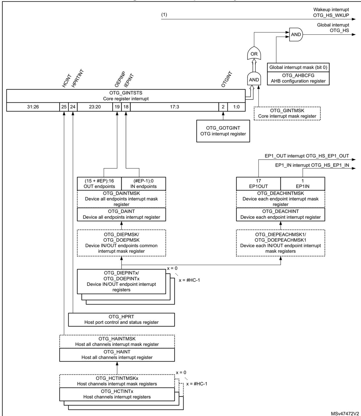
The diagram illustrates the interrupt hierarchy for the OTG_HS USB controller. At the top, a 'Wakeup interrupt OTG_HS_WKUP' signal is shown. Below it, the 'Global interrupt OTG_HS' is the output of an AND gate. This AND gate also takes inputs from an OR gate and the 'Global interrupt mask (bit 0)' from the 'OTG_AHBCFG' register. The OR gate receives inputs from the 'OTG_GINTSTS' register and the 'OTG_GOTGINT' register. The 'OTG_GINTSTS' register is a 32-bit core register interrupt with the following bit fields: 31:26 (reserved), 25 (HCINT), 24 (HPRTINT), 23:20 (reserved), 19 (CEPINT), 18 (IEPINT), 17:3 (reserved), 2 (OTGINT), and 1:0 (reserved). The 'OTG_GOTGINT' register is an OTG interrupt register. Below the 'OTG_GINTSTS' register, the 'OTG_DINTMSK' register (Device all endpoints interrupt mask register) and 'OTG_DINT' register (Device all endpoints interrupt register) are shown. These are further detailed by the 'OTG_DIEPMSK/OTG_DOEPMSK' (Device IN/OUT endpoints common interrupt mask register) and 'OTG_DIEPINTx/OTG_DOEPINTx' (Device IN/OUT endpoint interrupt registers) for x = 0 to x = #HC-1. The 'OTG_HPRT' register (Host port control and status register) is also shown. Below it, the 'OTG_HAINTMSK' (Host all channels interrupt mask register) and 'OTG_HAINT' (Host all channels interrupt register) are shown. These are further detailed by the 'OTG_HCTINTMSKx' (Host channels interrupt mask registers) and 'OTG_HCTINTx' (Host channels interrupt registers) for x = 0 to x = #HC-1. On the right side, the 'EP1_OUT interrupt OTG_HS_EP1_OUT' and 'EP1_IN interrupt OTG_HS_EP1_IN' are shown. These are further detailed by the 'OTG_DEACHINTMSK' (Device each endpoint interrupt mask register) and 'OTG_DEACHINT' (Device each endpoint interrupt register) for EP1OUT and EP1IN. These are further detailed by the 'OTG_DIEPEACHMSK1/OTG_DOEPEACHMSK1' (Device each IN/OUT endpoint interrupt mask registers).
- 1. OTG_HS_WKUP becomes active (high state) when resume condition occurs during L1 SLEEP or L2 SUSPEND states.
35.12 OTG_HS control and status registers
By reading from and writing to the control and status registers (CSRs) through the AHB slave interface, the application controls the OTG_HS controller. These registers are 32 bits wide, and the addresses are 32-bit block aligned. The OTG_HS registers must be accessed by words (32 bits). CSRs are classified as follows:
- • Core global registers
- • Host-mode registers
- • Host global registers
- • Host port CSRs
- • Host channel-specific registers
- • Device-mode registers
- • Device global registers
- • Device endpoint-specific registers
- • Power and clock-gating registers
- • Data FIFO (DFIFO) access registers
Only the Core global, Power and clock-gating, Data FIFO access, and host port control and status registers can be accessed in both host and peripheral modes. When the OTG_HS controller is operating in one mode, either peripheral or host, the application must not access registers from the other mode. If an illegal access occurs, a mode mismatch interrupt is generated and reflected in the Core interrupt register (MMIS bit in the OTG_HS_GINTSTS register). When the core switches from one mode to the other, the registers in the new mode of operation must be reprogrammed as they would be after a power-on reset.
35.12.1 CSR memory map
The host and peripheral mode registers occupy different addresses. All registers are implemented in the AHB clock domain.
Figure 415. CSR memory map
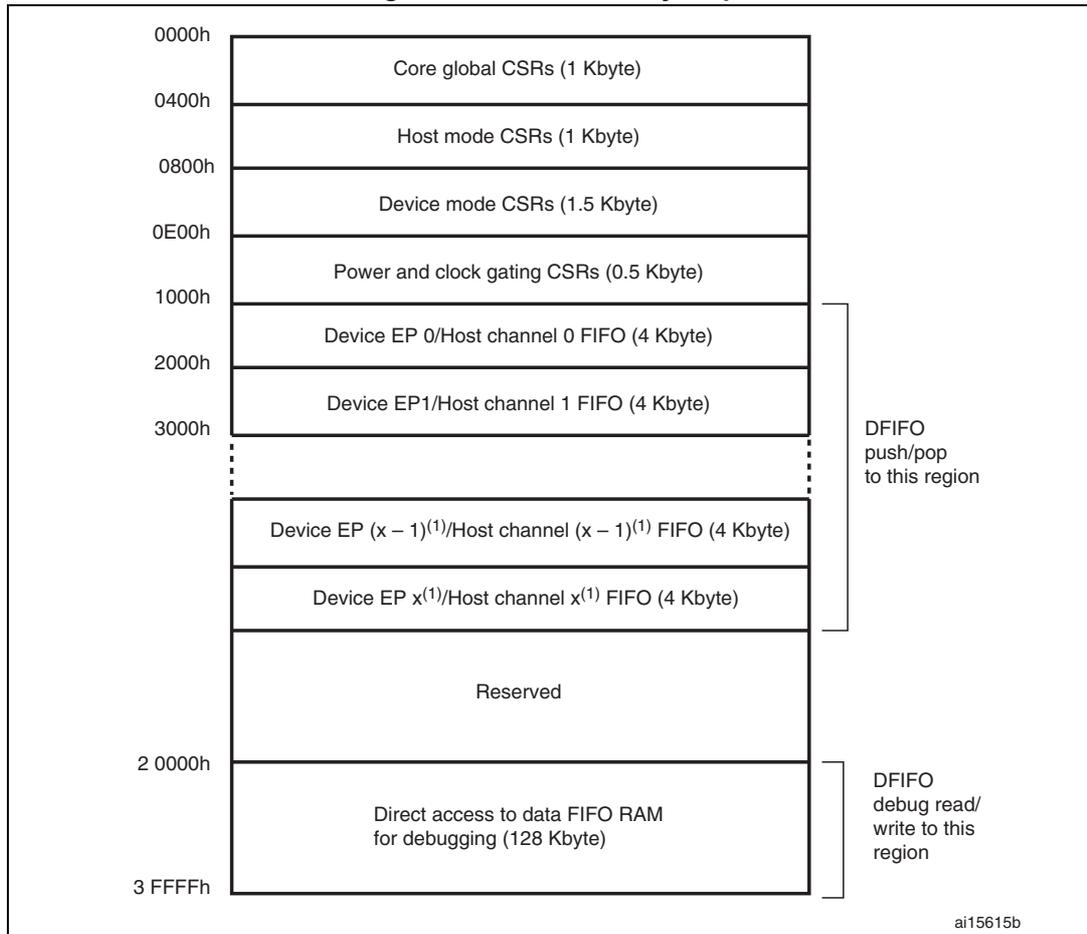
ai15615b
1. x = 5 in peripheral mode and x = 11 in host mode.
Global CSR map
These registers are available in both host and peripheral modes.
Table 209. Core global control and status registers (CSRs)
| Acronym | Address offset | Register name |
|---|---|---|
| OTG_HS_GOTGCTL | 0x000 | OTG_HS control and status register (OTG_HS_GOTGCTL) on page 1411 |
| OTG_HS_GOTGINT | 0x004 | OTG_HS interrupt register (OTG_HS_GOTGINT) on page 1412 |
| OTG_HS_GAHBCFG | 0x008 | OTG_HS AHB configuration register (OTG_HS_GAHBCFG) on page 1414 |
| OTG_HS_GUSBCFG | 0x00C | OTG_HS USB configuration register (OTG_HS_GUSBCFG) on page 1415 |
| OTG_HS_GRSTCTL | 0x010 | OTG_HS reset register (OTG_HS_GRSTCTL) on page 1418 |
| OTG_HS_GINTSTS | 0x014 | OTG_HS core interrupt register (OTG_HS_GINTSTS) on page 1421 |
| OTG_HS_GINTMSK | 0x018 | OTG_HS interrupt mask register (OTG_HS_GINTMSK) on page 1425 |
| Acronym | Address offset | Register name |
|---|---|---|
| OTG_HS_GRXSTSR | 0x01C | OTG_HS Receive status debug read/OTG status read and pop registers (OTG_HS_GRXSTSR/OTG_HS_GRXSTSP) on page 1428 |
| OTG_HS_GRXSTSP | 0x020 | |
| OTG_HS_GRXFSIZ | 0x024 | OTG_HS Receive FIFO size register (OTG_HS_GRXFSIZ) on page 1429 |
| OTG_HS_GNPTXFSIZ/ OTG_HS_TX0FSIZ | 0x028 | OTG_HS nonperiodic transmit FIFO size/Endpoint 0 transmit FIFO size register (OTG_HS_GNPTXFSIZ/OTG_HS_TX0FSIZ) on page 1430 |
| OTG_HS_GNPTXSTS | 0x02C | OTG_HS nonperiodic transmit FIFO/queue status register (OTG_HS_GNPTXSTS) on page 1430 |
| OTG_HS_GCCFG | 0x038 | OTG_HS general core configuration register (OTG_HS_GCCFG) on page 1431 |
| OTG_HS_CID | 0x03C | OTG_HS core ID register (OTG_HS_CID) on page 1432 |
| OTG_HS_HPTXFSIZ | 0x100 | OTG_HS Host periodic transmit FIFO size register (OTG_HS_HPTXFSIZ) on page 1432 |
| OTG_HS_DIEPTXFx | 0x104 0x108 ... 0x114 | OTG_HS device IN endpoint transmit FIFO size register (OTG_HS_DIEPTXFx) (x = 1..5, where x is the FIFO_number) on page 1433 |
These registers must be programmed every time the core changes to host mode.
Table 210. Host-mode control and status registers (CSRs)| Acronym | Offset address | Register name |
|---|---|---|
| OTG_HS_HCFG | 0x400 | OTG_HS host configuration register (OTG_HS_HCFG) on page 1433 |
| OTG_HS_HFIR | 0x404 | OTG_HS Host frame interval register (OTG_HS_HFIR) on page 1435 |
| OTG_HS_HFNUM | 0x408 | OTG_HS host frame number/frame time remaining register (OTG_HS_HFNUM) on page 1435 |
| OTG_HS_HPTXSTS | 0x410 | OTG_HS Host periodic transmit FIFO/queue status register (OTG_HS_HPTXSTS) on page 1436 |
| OTG_HS_HAINT | 0x414 | OTG_HS Host all channels interrupt register (OTG_HS_HAINT) on page 1437 |
| OTG_HS_HAINTMSK | 0x418 | OTG_HS host all channels interrupt mask register (OTG_HS_HAINTMSK) on page 1437 |
| OTG_HS_HPRT | 0x440 | OTG_HS host port control and status register (OTG_HS_HPRT) on page 1438 |
Table 210. Host-mode control and status registers (CSRs) (continued)
| Acronym | Offset address | Register name |
|---|---|---|
| OTG_HS_HCCHARx | 0x500 0x520 ... 0x660 | OTG_HS host channel-x characteristics register (OTG_HS_HCCHARx) (x = 0..11, where x = Channel_number) on page 1440 |
| OTG_HS_HCSPLTx | 0x504 | OTG_HS host channel-x split control register (OTG_HS_HCSPLTx) (x = 0..11, where x = Channel_number) on page 1442 |
| OTG_HS_HCINTx | 0x508 | OTG_HS host channel-x interrupt register (OTG_HS_HCINTx) (x = 0..11, where x = Channel_number) on page 1443 |
| OTG_HS_HCINTMSKx | 0x50C | OTG_HS host channel-x interrupt mask register (OTG_HS_HCINTMSKx) (x = 0..11, where x = Channel_number) on page 1444 |
| OTG_HS_HCTSIZx | 0x510 | OTG_HS host channel-x transfer size register (OTG_HS_HCTSIZx) (x = 0..11, where x = Channel_number) on page 1445 |
| OTG_HS_HCDMAx | 0x514 | OTG_HS host channel-x DMA address register (OTG_HS_HCDMAx) (x = 0..11, where x = Channel_number) on page 1446 |
Device-mode CSR map
These registers must be programmed every time the core changes to peripheral mode.
Table 211. Device-mode control and status registers
| Acronym | Offset address | Register name |
|---|---|---|
| OTG_HS_DCFG | 0x800 | OTG_HS device configuration register (OTG_HS_DCFG) on page 1446 |
| OTG_HS_DCTL | 0x804 | OTG_HS device control register (OTG_HS_DCTL) on page 1448 |
| OTG_HS_DSTS | 0x808 | OTG_HS device status register (OTG_HS_DSTS) on page 1450 |
| OTG_HS_DIEPMSK | 0x810 | OTG_HS device IN endpoint common interrupt mask register (OTG_HS_DIEPMSK) on page 1451 |
| OTG_HS_DOEPMSK | 0x814 | OTG_HS device OUT endpoint common interrupt mask register (OTG_HS_DOEPMSK) on page 1452 |
| OTG_HS_DAINT | 0x818 | OTG_HS device all endpoints interrupt register (OTG_HS_DAINT) on page 1453 |
| OTG_HS_DAINTMSK | 0x81C | OTG_HS all endpoints interrupt mask register (OTG_HS_DAINTMSK) on page 1454 |
| OTG_HS_DVBUSDIS | 0x828 | OTG_HS device V BUS discharge time register (OTG_HS_DVBUSDIS) on page 1454 |
| OTG_HS_DVBUSPULSE | 0x82C | OTG_HS device V BUS pulsing time register (OTG_HS_DVBUSPULSE) on page 1455 |
| OTG_HS_DTHRCTL | 0x830 | OTG_HS Device threshold control register (OTG_HS_DTHRCTL) on page 1456 |
Table 211. Device-mode control and status registers (continued)
| Acronym | Offset address | Register name |
|---|---|---|
| OTG_HS_DIEPEMPMSK | 0x834 | OTG_HS device IN endpoint FIFO empty interrupt mask register: (OTG_HS_DIEPEMPMSK) on page 1457 |
| OTG_HS_DEACHINT | 0x838 | OTG_HS device each endpoint interrupt register (OTG_HS_DEACHINT) on page 1457 |
| OTG_HS_DEACHINTMSK | 0x83C | OTG_HS device each endpoint interrupt register mask (OTG_HS_DEACHINTMSK) on page 1458 |
| OTG_HS_DIEPEACHMSK1 | 0x844 | OTG_HS device each in endpoint-1 interrupt register (OTG_HS_DIEPEACHMSK1) on page 1458 |
| OTG_HS_DOEPEACHMSK1 | 0x884 | OTG_HS device each OUT endpoint-1 interrupt register (OTG_HS_DOEPEACHMSK1) on page 1459 |
| OTG_HS_DIEPCTLx | 0x900 0x920 ... 0x9A0 | OTG device endpoint-x control register (OTG_HS_DIEPCTLx) (x = 0..5, where x = Endpoint_number) on page 1460 |
| OTG_HS_DIEPINTx | 0x908 | OTG_HS device endpoint-x interrupt register (OTG_HS_DIEPINTx) (x = 0..5, where x = Endpoint_number) on page 1467 |
| OTG_HS_DIEPTSIZ0 | 0x910 | OTG_HS device IN endpoint 0 transfer size register (OTG_HS_DIEPTSIZ0) on page 1470 |
| OTG_HS_DIEPDMAx/ OTG_HS_DOEPDMAx | 0x914/0xB14 | OTG_HS device endpoint-x DMA address register (OTG_HS_DIEPDMAx / OTG_HS_DOEPDMAx) (x = 0..5, where x = Endpoint_number) on page 1474 |
| OTG_HS_DTXFSTSx | 0x918 | OTG_HS device IN endpoint transmit FIFO status register (OTG_HS_DTXFSTSx) (x = 0..5, where x = Endpoint_number) on page 1473 |
| OTG_HS_DIEPTSIZx | 0x930 0x950 ... 0x9B0 | OTG_HS device endpoint-x transfer size register (OTG_HS_DIEPTSIZx) (x = 1..5, where x = Endpoint_number) on page 1472 |
| OTG_HS_DOEPCTL0 | 0xB00 | OTG_HS device control OUT endpoint 0 control register (OTG_HS_DOEPCTL0) on page 1463 |
| OTG_HS_DOEPSIZ0 | 0xB10 | OTG_HS device OUT endpoint 0 transfer size register (OTG_HS_DOEPSIZ0) on page 1471 |
| OTG_HS_DOEPCTLx | 0xB20 0xB40 ... 0xBA0 | OTG_HS device endpoint-x control register (OTG_HS_DOEPCTLx) (x = 1..5, where x = Endpoint_number) on page 1464 |
Table 211. Device-mode control and status registers (continued)
| Acronym | Offset address | Register name |
|---|---|---|
| OTG_HS_DOEPINTx | 0xB08 0xB28 ... 0xBA8 | OTG_HS device endpoint-x interrupt register (OTG_HS_DOEPINTx) (x = 0..5, where x = Endpoint_number) on page 1469 |
| OTG_HS_DOEPTSIZx | 0xB30 0xB50 ... 0xBB0 | OTG_HS device endpoint-x transfer size register (OTG_HS_DOEPTSIZx) (x = 1..5, where x = Endpoint_number) on page 1473 |
Data FIFO (DFIFO) access register map
These registers, available in both host and peripheral modes, are used to read or write the FIFO space for a specific endpoint or a channel, in a given direction. If a host channel is of type IN, the FIFO can only be read on the channel. Similarly, if a host channel is of type OUT, the FIFO can only be written on the channel.
Table 212. Data FIFO (DFIFO) access register map
| FIFO access register section | Address range | Access |
|---|---|---|
| Device IN Endpoint 0/Host OUT Channel 0: DFIFO Write Access Device OUT Endpoint 0/Host IN Channel 0: DFIFO Read Access | 0x1000–0x1FFC | w r |
| Device IN Endpoint 1/Host OUT Channel 1: DFIFO Write Access Device OUT Endpoint 1/Host IN Channel 1: DFIFO Read Access | 0x2000–0x2FFC | w r |
| ... | ... | ... |
| Device IN Endpoint x
(1)
/Host OUT Channel x
(1)
: DFIFO Write Access Device OUT Endpoint x (1) /Host IN Channel x (1) : DFIFO Read Access | 0xX000–0xXFFC | w r |
1. Where x is 5 in peripheral mode and 11 in host mode.
Power and clock gating CSR map
There is a single register for power and clock gating. It is available in both host and peripheral modes.
Table 213. Power and clock gating control and status registers
| Register name | Acronym | Offset address: 0xE00–0xFFF |
|---|---|---|
| Power and clock gating control register | OTG_HS_PCGCTL | 0xE00–0xE04 |
| Reserved | - | 0xE05–0xFFF |
35.12.2 OTG_HS global registers
These registers are available in both host and peripheral modes, and do not need to be reprogrammed when switching between these modes.
Bit values in the register descriptions are expressed in binary unless otherwise specified.
OTG_HS control and status register (OTG_HS_GOTGCTL)
Address offset: 0x000
Reset value: 0x0001 0000
The OTG control and status register controls the behavior and reflects the status of the OTG function of the core.
| 31 | 30 | 29 | 28 | 27 | 26 | 25 | 24 | 23 | 22 | 21 | 20 | 19 | 18 | 17 | 16 | 15 | 14 | 13 | 12 | 11 | 10 | 9 | 8 | 7 | 6 | 5 | 4 | 3 | 2 | 1 | 0 |
| Reserved | BSVLD | ASVLD | DBCT | CIDSTS | Reserved | DHNPEN | HSHNPEN | HNPRQ | HNGSCS | Reserved | SRQ | SRQSCS | |||||||||||||||||||
| r | r | r | r | rw | rw | rw | r | rw | r | ||||||||||||||||||||||
Bits 31:20 Reserved, must be kept at reset value.
Bit 19 BSVLD : B-session valid
Indicates the peripheral mode transceiver status.
0: B-session is not valid.
1: B-session is valid.
In OTG mode, you can use this bit to determine if the device is connected or disconnected.
Note: Only accessible in peripheral mode.
Bit 18 ASVLD : A-session valid
Indicates the host mode transceiver status.
0: A-session is not valid
1: A-session is valid
Note: Only accessible in host mode.
Bit 17 DBCT : Long/short debounce time
Indicates the debounce time of a detected connection.
0: Long debounce time, used for physical connections (100 ms + 2.5 µs)
1: Short debounce time, used for soft connections (2.5 µs)
Note: Only accessible in host mode.
Bit 16 CIDSTS : Connector ID status
Indicates the connector ID status on a connect event.
0: The OTG_HS controller is in A-device mode
1: The OTG_HS controller is in B-device mode
Note: Accessible in both peripheral and host modes.
Bits 15:12 Reserved, must be kept at reset value.
Bit 11 DHNPEN : Device HNP enabled
The application sets this bit when it successfully receives a SetFeature.SetHNPEnable command from the connected USB host.
0: HNP is not enabled in the application
1: HNP is enabled in the application
Note: Only accessible in peripheral mode.
Bit 10 HSHNPEN: Host set HNP enable
The application sets this bit when it has successfully enabled HNP (using the SetFeature.SetHNPEnable command) on the connected device.
0: Host Set HNP is not enabled
1: Host Set HNP is enabled
Note: Only accessible in host mode.
Bit 9 HNPRQ: HNP request
The application sets this bit to initiate an HNP request to the connected USB host. The application can clear this bit by writing a 0 when the host negotiation success status change bit in the OTG interrupt register (HNSSCHG bit in OTG_HS_GOTGINT) is set. The core clears this bit when the HNSSCHG bit is cleared.
0: No HNP request
1: HNP request
Note: Only accessible in peripheral mode.
Bit 8 HNGSCS: Host negotiation success
The core sets this bit when host negotiation is successful. The core clears this bit when the HNP Request (HNPRQ) bit in this register is set.
0: Host negotiation failure
1: Host negotiation success
Note: Only accessible in peripheral mode.
Bits 7:2 Reserved, must be kept at reset value.
Bit 1 SRQ: Session request
The application sets this bit to initiate a session request on the USB. The application can clear this bit by writing a 0 when the host negotiation success status change bit in the OTG Interrupt register (HNSSCHG bit in OTG_HS_GOTGINT) is set. The core clears this bit when the HNSSCHG bit is cleared.
If you use the USB 1.1 full-speed serial transceiver interface to initiate the session request, the application must wait until
\(
V_{BUS}
\)
discharges to 0.2 V, after the B-Session Valid bit in this register (BSVLD bit in OTG_HS_GOTGCTL) is cleared.
0: No session request
1: Session request
Note: Only accessible in peripheral mode.
Bit 0 SRQSCS: Session request success
The core sets this bit when a session request initiation is successful.
0: Session request failure
1: Session request success
Note: Only accessible in peripheral mode.
OTG_HS interrupt register (OTG_HS_GOTGINT)
Address offset: 0x04
Reset value: 0x0000 0000
The application reads this register whenever there is an OTG interrupt and clears the bits in this register to clear the OTG interrupt.
| 31 | 30 | 29 | 28 | 27 | 26 | 25 | 24 | 23 | 22 | 21 | 20 | 19 | 18 | 17 | 16 | 15 | 14 | 13 | 12 | 11 | 10 | 9 | 8 | 7 | 6 | 5 | 4 | 3 | 2 | 1 | 0 |
| Reserved | DBCDNE | ADTOCHG | HNGDET | Reserved | HNSSCHG | SRSSCHG | Reserved | SEDET | Res. | ||||||||||||||||||||||
| rc_ w1 | rc_ w1 | rc_ w1 | rc_ w1 | rc_ w1 | rc_ w1 | ||||||||||||||||||||||||||
Bits 31:20 Reserved, must be kept at reset value.
Bit 19 DBCDNE : Debounce done
The core sets this bit when the debounce is completed after the device connect. The application can start driving USB reset after seeing this interrupt. This bit is only valid when the HNP Capable or SRP Capable bit is set in the Core USB Configuration register (HNPCAP bit or SRPCAP bit in OTG_HS_GUSBCFG, respectively).
Note: Only accessible in host mode.
Bit 18 ADTOCHG : A-device timeout change
The core sets this bit to indicate that the A-device has timed out while waiting for the B-device to connect.
Note: Accessible in both peripheral and host modes.
Bit 17 HNGDET : Host negotiation detected
The core sets this bit when it detects a host negotiation request on the USB.
Note: Accessible in both peripheral and host modes.
Bits 16:10 Reserved, must be kept at reset value.
Bit 9 HNSSCHG : Host negotiation success status change
The core sets this bit on the success or failure of a USB host negotiation request. The application must read the host negotiation success bit of the OTG Control and Status register (HNGSCS in OTG_HS_GOTGCTL) to check for success or failure.
Note: Accessible in both peripheral and host modes.
Bits 7:3 Reserved, must be kept at reset value.
Bit 8 SRSSCHG : Session request success status change
The core sets this bit on the success or failure of a session request. The application must read the session request success bit in the OTG Control and status register (SRQSCS bit in OTG_HS_GOTGCTL) to check for success or failure.
Note: Accessible in both peripheral and host modes.
Bit 2 SEDET : Session end detected
The core sets this bit to indicate that the level of the voltage on \( V_{BUS} \) is no longer valid for a B-device session when \( V_{BUS} < 0.8\text{ V} \) .
Bits 1:0 Reserved, must be kept at reset value.
OTG_HS AHB configuration register (OTG_HS_GAHBCFG)
Address offset: 0x008
Reset value: 0x0000 0000
This register can be used to configure the core after power-on or a change in mode. This register mainly contains AHB system-related configuration parameters. Do not change this register after the initial programming. The application must program this register before starting any transactions on either the AHB or the USB.
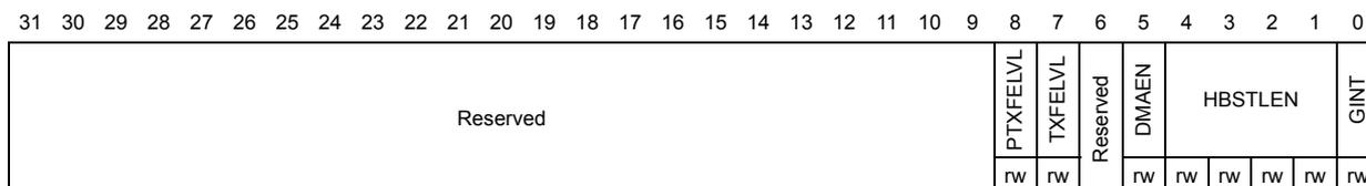
| 31 | 30 | 29 | 28 | 27 | 26 | 25 | 24 | 23 | 22 | 21 | 20 | 19 | 18 | 17 | 16 | 15 | 14 | 13 | 12 | 11 | 10 | 9 | 8 | 7 | 6 | 5 | 4 | 3 | 2 | 1 | 0 | ||
| Reserved | PTXFELVL | TXFELVL | Reserved | DMAEN | HBSTLEN | GINT | |||||||||||||||||||||||||||
| rw | rw | rw | rw | rw | rw | rw | |||||||||||||||||||||||||||
Bits 31:20 Reserved, must be kept at reset value.
Bit 8 PTXFELVL : Periodic TxFIFO empty level
Indicates when the periodic TxFIFO empty interrupt bit in the Core interrupt register (PTXFE bit in OTG_HS_GINTSTS) is triggered.
0: PTXFE (in OTG_HS_GINTSTS) interrupt indicates that the Periodic TxFIFO is half empty
1: PTXFE (in OTG_HS_GINTSTS) interrupt indicates that the Periodic TxFIFO is completely empty
Note: Only accessible in host mode.
Bit 7 TXFELVL : TxFIFO empty level
In peripheral mode, this bit indicates when the IN endpoint Transmit FIFO empty interrupt (TXFE in OTG_HS_DIEPINTx.) is triggered.
0: TXFE (in OTG_HS_DIEPINTx) interrupt indicates that the IN Endpoint TxFIFO is half empty
1: TXFE (in OTG_HS_DIEPINTx) interrupt indicates that the IN Endpoint TxFIFO is completely empty
Note: Only accessible in peripheral mode.
Bit 6 Reserved, must be kept at reset value.
Bits 5 DMAEN : DMA enable
0: The core operates in slave mode
1: The core operates in DMA mode
Bits 4:1 HBSTLEN : Burst length/type
0000 Single
0001 INCR
0011 INCR4
0101 INCR8
0111 INCR16
Others: Reserved
Bit 0 GINT : Global interrupt mask
This bit is used to mask or unmask the interrupt line assertion to the application. Irrespective of this bit setting, the interrupt status registers are updated by the core.
0: Mask the interrupt assertion to the application.
1: Unmask the interrupt assertion to the application
Note: Accessible in both peripheral and host modes.
OTG_HS USB configuration register (OTG_HS_GUSBCFG)
Address offset: 0x00C
Reset value: 0x0000 1440
This register can be used to configure the core after power-on or a changing to host mode or peripheral mode. It contains USB and USB-PHY related configuration parameters. The application must program this register before starting any transactions on either the AHB or the USB. Do not make changes to this register after the initial programming.
| 31 | 30 | 29 | 28 | 27 | 26 | 25 | 24 | 23 | 22 | 21 | 20 | 19 | 18 | 17 | 16 | 15 | 14 | 13 | 12 | 11 | 10 | 9 | 8 | 7 | 6 | 5 | 4 | 3 | 2 | 1 | 0 |
|---|---|---|---|---|---|---|---|---|---|---|---|---|---|---|---|---|---|---|---|---|---|---|---|---|---|---|---|---|---|---|---|
| CTXPKT | FDMOD | FHMOD | Reserved | ULPIIPD | PTCI | PCCI | TSDPS | ULPIEVBUSI | ULPIEVBUSD | ULPICSM | ULPIAR | ULPISLS | Reserved | PHYLPCS | Reserved | TRDT | HNPCAP | SRPCAP | Reserved | PHYSEL | Reserved | TOCAL | |||||||||
| rw | rw | rw | rw | rw | rw | rw | rw | rw | rw | rw | rw | rw | rw | rw | |||||||||||||||||
Bit 31 CTXPKT : Corrupt Tx packet
This bit is for debug purposes only. Never set this bit to 1.
Note: Accessible in both peripheral and host modes.
Bit 30 FDMOD : Forced peripheral mode
Writing a 1 to this bit forces the core to peripheral mode irrespective of the OTG_HS_ID input pin.
0: Normal mode
1: Forced peripheral mode
After setting the force bit, the application must wait at least 25 ms before the change takes effect.
Note: Accessible in both peripheral and host modes.
Bit 29 FHMOD : Forced host mode
Writing a 1 to this bit forces the core to host mode irrespective of the OTG_HS_ID input pin.
0: Normal mode
1: Forced host mode
After setting the force bit, the application must wait at least 25 ms before the change takes effect.
Note: Accessible in both peripheral and host modes.
Bits 28:26 Reserved, must be kept at reset value.
Bit 25 ULPIIPD : ULPI interface protect disable
This bit controls the circuitry built in the PHY to protect the ULPI interface when the link tri-states stop and data. Any pull-up or pull-down resistors employed by this feature can be disabled. Please refer to the ULPI specification for more details.
0: Enables the interface protection circuit
1: Disables the interface protection circuit
Bit 24 PTCI : Indicator pass through
This bit controls whether the complement output is qualified with the internal V BUS valid comparator before being used in the V BUS state in the RX CMD. Please refer to the ULPI specification for more details.
0: Complement Output signal is qualified with the Internal V BUS valid comparator
1: Complement Output signal is not qualified with the Internal V BUS valid comparator
Bit 23 PCCI: Indicator complementThis bit controls the PHY to invert the ExternalVbusIndicator input signal, and generate the complement output. Please refer to the ULPI specification for more details.
0: PHY does not invert the ExternalVbusIndicator signal
1: PHY inverts ExternalVbusIndicator signal
Bit 22 TSDPS: TermSel DLine pulsing selectionThis bit selects utmi_termselect to drive the data line pulse during SRP (session request protocol).
0: Data line pulsing using utmi_txvalid (default)
1: Data line pulsing using utmi_termsel
Bit 21 ULPIEVBUSI: ULPI external V BUS indicatorThis bit indicates to the ULPI PHY to use an external V BUS overcurrent indicator.
0: PHY uses an internal V BUS valid comparator
1: PHY uses an external V BUS valid comparator
Bit 20 ULPIEVBUSD: ULPI External V BUS DriveThis bit selects between internal or external supply to drive 5 V on V BUS , in the ULPI PHY.
0: PHY drives V BUS using internal charge pump (default)
1: PHY drives V BUS using external supply.
Bit 19 ULPICSM: ULPI Clock SuspendMThis bit sets the ClockSuspendM bit in the interface control register on the ULPI PHY. This bit applies only in the serial and carkit modes.
0: PHY powers down the internal clock during suspend
1: PHY does not power down the internal clock
Bit 18 ULPIAR: ULPI Auto-resumeThis bit sets the AutoResume bit in the interface control register on the ULPI PHY.
0: PHY does not use AutoResume feature
1: PHY uses AutoResume feature
Bit 17 ULPIFSL: ULPI FS/LS selectThe application uses this bit to select the FS/LS serial interface for the ULPI PHY. This bit is valid only when the FS serial transceiver is selected on the ULPI PHY.
0: ULPI interface
1: ULPI FS/LS serial interface
Bit 16 Reserved, must be kept at reset value. Bit 15 PHYLPCS: PHY Low-power clock selectThis bit selects either 480 MHz or 48 MHz (low-power) PHY mode. In FS and LS modes, the PHY can usually operate on a 48 MHz clock to save power.
0: 480 MHz internal PLL clock
1: 48 MHz external clock
In 480 MHz mode, the UTMI interface operates at either 60 or 30 MHz, depending on whether the 8- or 16-bit data width is selected. In 48 MHz mode, the UTMI interface operates at 48 MHz in FS and LS modes.
Bit 14 Reserved, must be kept at reset value. Bits 13:10 TRDT: USB turnaround timeThese bits allow to set the turnaround time in PHY clocks. They must be configured according to Table 214: TRDT values , depending on the application AHB frequency. Higher TRDT values allow stretching the USB response time to IN tokens in order to compensate for longer AHB read access latency to the Data FIFO.
Bit 9 HNPCAP : HNP-capableThe application uses this bit to control the OTG_HS controller's HNP capabilities.
0: HNP capability is not enabled
1: HNP capability is enabled
Note: Accessible in both peripheral and host modes.
Bit 8 SRPCAP : SRP-capableThe application uses this bit to control the OTG_HS controller's SRP capabilities. If the core operates as a nonSRP-capable B-device, it cannot request the connected A-device (host) to activate V BUS and start a session.
0: SRP capability is not enabled
1: SRP capability is enabled
Note: Accessible in both peripheral and host modes.
Bit 7 Reserved, must be kept at reset value.
Bit 6 PHYSEL : USB 2.0 high-speed ULPI PHY or USB 1.1 full-speed serial transceiver select0: USB 2.0 high-speed ULPI PHY
1: USB 1.1 full-speed serial transceiver
Bits 5:3 Reserved, must be kept at reset value.
Bits 2:0 TOCAL : FS timeout calibrationThe number of PHY clocks that the application programs in this field is added to the full-speed interpacket timeout duration in the core to account for any additional delays introduced by the PHY. This can be required, because the delay introduced by the PHY in generating the line state condition can vary from one PHY to another.
The USB standard timeout value for full-speed operation is 16 to 18 (inclusive) bit times. The application must program this field based on the speed of enumeration. The number of bit times added per PHY clock is 0.25 bit times.
Table 214. TRDT values
| AHB frequency range (MHz) | TRDT minimum value | |
|---|---|---|
| Min. | Max | |
| 30 | - | 0x9 |
OTG_HS reset register (OTG_HS_GRSTCTL)
Address offset: 0x010
Reset value: 0x8000 0000
The application uses this register to reset various hardware features inside the core.
| 31 | 30 | 29 | 28 | 27 | 26 | 25 | 24 | 23 | 22 | 21 | 20 | 19 | 18 | 17 | 16 | 15 | 14 | 13 | 12 | 11 | 10 | 9 | 8 | 7 | 6 | 5 | 4 | 3 | 2 | 1 | 0 | |
|---|---|---|---|---|---|---|---|---|---|---|---|---|---|---|---|---|---|---|---|---|---|---|---|---|---|---|---|---|---|---|---|---|
| AHBIDL | DMAREQ | Reserved | TXFNUM | TXFFLSH | RXFFLSH | Reserved | FCRST | HSRST | CSRST | |||||||||||||||||||||||
| r | r | rw | rs | rs | rs | rs | rs | |||||||||||||||||||||||||
Bit 31 AHBIDL : AHB master idle
Indicates that the AHB master state machine is in the Idle condition.
Note: Accessible in both peripheral and host modes.
Bit 30 DMAREQ : DMA request signal
This bit indicates that the DMA request is in progress. Used for debug.
Bits 29:11 Reserved, must be kept at reset value.
Bits 10:6 TXFNUM : TxFIFO number
This is the FIFO number that must be flushed using the TxFIFO Flush bit. This field must not be changed until the core clears the TxFIFO Flush bit.
00000:
- - Nonperiodic TxFIFO flush in host mode
- - Tx FIFO 0 flush in peripheral mode
00001:
- - Periodic TxFIFO flush in host mode
- - TXFIFO 1 flush in peripheral mode
00010: TXFIFO 2 flush in peripheral mode
...
00101: TXFIFO 15 flush in peripheral mode
10000: Flush all the transmit FIFOs in peripheral or host mode.
Note: Accessible in both peripheral and host modes.
Bit 5 TXFFLSH : TxFIFO flush
This bit selectively flushes a single or all transmit FIFOs, but cannot do so if the core is in the midst of a transaction.
The application must write this bit only after checking that the core is neither writing to the TxFIFO nor reading from the TxFIFO. Verify using these registers:
- - Read: the NAK effective interrupt ensures the core is not reading from the FIFO
- - Write: the AHBIDL bit in OTG_HS_GRSTCTL ensures that the core is not writing anything to the FIFO
Note: Accessible in both peripheral and host modes.
Bit 4 RXFFLSH: RxFIFO flushThe application can flush the entire RxFIFO using this bit, but must first ensure that the core is not in the middle of a transaction.
The application must only write to this bit after checking that the core is neither reading from the RxFIFO nor writing to the RxFIFO.
The application must wait until the bit is cleared before performing any other operation. This bit requires 8 clocks (slowest of PHY or AHB clock) to be cleared.
Note: Accessible in both peripheral and host modes.
Bit 3 Reserved, must be kept at reset value. Bit 2 FCRST: Host frame counter resetThe application writes this bit to reset the (micro) frame number counter inside the core. When the (micro) frame counter is reset, the subsequent SOF sent out by the core has a frame number of 0.
Note: Only accessible in host mode.
Bit 1 HSRST: HCLK soft resetThe application uses this bit to flush the control logic in the AHB Clock domain. Only AHB Clock Domain pipelines are reset.
FIFOs are not flushed with this bit.
All state machines in the AHB clock domain are reset to the Idle state after terminating the transactions on the AHB, following the protocol.
CSR control bits used by the AHB clock domain state machines are cleared.
To clear this interrupt, status mask bits that control the interrupt status and are generated by the AHB clock domain state machine are cleared.
Because interrupt status bits are not cleared, the application can get the status of any core events that occurred after it set this bit.
This is a self-clearing bit that the core clears after all necessary logic is reset in the core. This can take several clocks, depending on the core's current state.
Note: Accessible in both peripheral and host modes.
Bit 0 CSRST: Core soft resetResets the HCLK and PCLK domains as follows:
Clears the interrupts and all the CSR register bits except for the following bits:
- – RSTPDMODL bit in OTG_HS_PCGCCTL
- – GAYEHCLK bit in OTG_HS_PCGCCTL
- – PWRCLMP bit in OTG_HS_PCGCCTL
- – STPPCLK bit in OTG_HS_PCGCCTL
- – FSLSPCS bit in OTG_HS_HCFG
- – DSPD bit in OTG_HS_DCFG
All module state machines (except for the AHB slave unit) are reset to the Idle state, and all the transmit FIFOs and the receive FIFO are flushed.
Any transactions on the AHB Master are terminated as soon as possible, after completing the last data phase of an AHB transfer. Any transactions on the USB are terminated immediately.
The application can write to this bit any time it wants to reset the core. This is a self-clearing bit and the core clears this bit after all the necessary logic is reset in the core, which can take several clocks, depending on the current state of the core. Once this bit has been cleared, the software must wait at least 3 PHY clocks before accessing the PHY domain (synchronization delay). The software must also check that bit 31 in this register is set to 1 (AHB Master is Idle) before starting any operation.
Typically, the software reset is used during software development and also when you dynamically change the PHY selection bits in the above listed USB configuration registers. When you change the PHY, the corresponding clock for the PHY is selected and used in the PHY domain. Once a new clock is selected, the PHY domain has to be reset for proper operation.
Note: Accessible in both peripheral and host modes.
OTG_HS core interrupt register (OTG_HS_GINTSTS)
Address offset: 0x014
Reset value: 0x0400 0020
This register interrupts the application for system-level events in the current mode (peripheral mode or host mode).
Some of the bits in this register are valid only in host mode, while others are valid in peripheral mode only. This register also indicates the current mode. To clear the interrupt status bits of the rc_w1 type, the application must write 1 into the bit.
The FIFO status interrupts are read-only; once software reads from or writes to the FIFO while servicing these interrupts, FIFO interrupt conditions are cleared automatically.
The application must clear the OTG_HS_GINTSTS register at initialization before unmasking the interrupt bit to avoid any interrupts generated prior to initialization.
| 31 | 30 | 29 | 28 | 27 | 26 | 25 | 24 | 23 | 22 | 21 | 20 | 19 | 18 | 17 | 16 | 15 | 14 | 13 | 12 | 11 | 10 | 9 | 8 | 7 | 6 | 5 | 4 | 3 | 2 | 1 | 0 |
|---|---|---|---|---|---|---|---|---|---|---|---|---|---|---|---|---|---|---|---|---|---|---|---|---|---|---|---|---|---|---|---|
| WKUPINT | SRQINT | DISCINT | CIDSCHG | Reserved | PTXFE | HCINT | HPRTINT | Reserved | DATAFSUSP | IPXFR/INCOMPISOUT | ISOXFR | OEPINT | IEPINT | Reserved | EOPF | ISOODRP | ENUMDNE | USBRST | USBSUSP | ESUSP | Reserved | GONAKEFF | GINAKEFF | NPTXFE | RXFLVL | SOF | OTGINT | MMIS | CMOD | ||
| rc_w1 | r | r | r | rc_w1 | r | r | rc_w1 | r | r | r | r | rc_w1 | r | rc_w1 | r | ||||||||||||||||
Bit 31 WKUPINT : Resume/remote wake-up detected interrupt
In peripheral mode, this interrupt is asserted when a resume is detected on the USB. In host mode, this interrupt is asserted when a remote wake-up is detected on the USB.
Note: Accessible in both peripheral and host modes.
Bit 30 SRQINT : Session request/new session detected interrupt
In host mode, this interrupt is asserted when a session request is detected from the device. In peripheral mode, this interrupt is asserted when \( V_{BUS} \) is in the valid range for a B-device device. Accessible in both peripheral and host modes.
Bit 29 DISCINT : Disconnect detected interrupt
Asserted when a device disconnect is detected.
Note: Only accessible in host mode.
Bit 28 CIDSCHG : Connector ID status change
The core sets this bit when there is a change in connector ID status.
Note: Accessible in both peripheral and host modes.
Bit 27 Reserved, must be kept at reset value.
Bit 26 PTXFE : Periodic TxFIFO empty
Asserted when the periodic transmit FIFO is either half or completely empty and there is space for at least one entry to be written in the periodic request queue. The half or completely empty status is determined by the periodic TxFIFO empty level bit in the Core AHB configuration register (PTXFELVL bit in OTG_HS_GAHBCFG).
Note: Only accessible in host mode.
Bit 25 HCINT: Host channels interruptThe core sets this bit to indicate that an interrupt is pending on one of the channels of the core (in host mode). The application must read the host all channels interrupt (OTG_HS_HAINT) register to determine the exact number of the channel on which the interrupt occurred, and then read the corresponding host channel-x interrupt (OTG_HS_HCINTx) register to determine the exact cause of the interrupt. The application must clear the appropriate status bit in the OTG_HS_HCINTx register to clear this bit.
Note: Only accessible in host mode.
Bit 24 HPRTINT: Host port interruptThe core sets this bit to indicate a change in port status of one of the OTG_HS controller ports in host mode. The application must read the host port control and status (OTG_HS_HPRT) register to determine the exact event that caused this interrupt. The application must clear the appropriate status bit in the host port control and status register to clear this bit.
Note: Only accessible in host mode.
Bits 23 Reserved, must be kept at reset value. Bit 22 DATAFSUSP: Data fetch suspendedThis interrupt is valid only in DMA mode. This interrupt indicates that the core has stopped fetching data for IN endpoints due to the unavailability of TxFIFO space or request queue space. This interrupt is used by the application for an endpoint mismatch algorithm. For example, after detecting an endpoint mismatch, the application:
- – Sets a global nonperiodic IN NAK handshake
- – Disables IN endpoints
- – Flushes the FIFO
- – Determines the token sequence from the IN token sequence learning queue
- – Re-enables the endpoints
- – Clears the global nonperiodic IN NAK handshake If the global nonperiodic IN NAK is cleared, the core has not yet fetched data for the IN endpoint, and the IN token is received: the core generates an “IN token received when FIFO empty” interrupt. The OTG then sends a NAK response to the host. To avoid this scenario, the application can check the FetSusp interrupt in OTG_HS_GINTSTS, which ensures that the FIFO is full before clearing a global NAK handshake. Alternatively, the application can mask the “IN token received when FIFO empty” interrupt when clearing a global IN NAK handshake.
In host mode, the core sets this interrupt bit when there are incomplete periodic transactions still pending, which are scheduled for the current frame.
Note: Only accessible in host mode.
INCOMPISOOUT: Incomplete isochronous OUT transferIn peripheral mode, the core sets this interrupt to indicate that there is at least one isochronous OUT endpoint on which the transfer is not completed in the current frame. This interrupt is asserted along with the End of periodic frame interrupt (EOPF) bit in this register.
Note: Only accessible in peripheral mode.
Bit 20 IISOIXFR: Incomplete isochronous IN transferThe core sets this interrupt to indicate that there is at least one isochronous IN endpoint on which the transfer is not completed in the current frame. This interrupt is asserted along with the End of periodic frame interrupt (EOPF) bit in this register.
Note: Only accessible in peripheral mode.
Bit 19 OEPINT: OUT endpoint interruptThe core sets this bit to indicate that an interrupt is pending on one of the OUT endpoints of the core (in peripheral mode). The application must read the device all endpoints interrupt (OTG_HS_DAIN) register to determine the exact number of the OUT endpoint on which the interrupt occurred, and then read the corresponding device OUT Endpoint-x Interrupt (OTG_HS_DOEPINTx) register to determine the exact cause of the interrupt. The application must clear the appropriate status bit in the corresponding OTG_HS_DOEPINTx register to clear this bit.
Note: Only accessible in peripheral mode.
Bit 18 IEPINT: IN endpoint interruptThe core sets this bit to indicate that an interrupt is pending on one of the IN endpoints of the core (in peripheral mode). The application must read the device All Endpoints Interrupt (OTG_HS_DAIN) register to determine the exact number of the IN endpoint on which the interrupt occurred, and then read the corresponding device IN Endpoint-x interrupt (OTG_HS_DIEPINTx) register to determine the exact cause of the interrupt. The application must clear the appropriate status bit in the corresponding OTG_HS_DIEPINTx register to clear this bit.
Note: Only accessible in peripheral mode.
Bits 17:16 Reserved, must be kept at reset value.
Bit 15 EOPF: End of periodic frame interruptIndicates that the period specified in the periodic frame interval field of the device configuration register (PFIVL bit in OTG_HS_DCFG) has been reached in the current frame.
Note: Only accessible in peripheral mode.
Bit 14 ISOODRP: Isochronous OUT packet dropped interruptThe core sets this bit when it fails to write an isochronous OUT packet into the RxFIFO because the RxFIFO does not have enough space to accommodate a maximum size packet for the isochronous OUT endpoint.
Note: Only accessible in peripheral mode.
Bit 13 ENUMDNE: Enumeration doneThe core sets this bit to indicate that speed enumeration is complete. The application must read the device Status (OTG_HS_DSTS) register to obtain the enumerated speed.
Note: Only accessible in peripheral mode.
Bit 12 USBRST: USB resetThe core sets this bit to indicate that a reset is detected on the USB.
Note: Only accessible in peripheral mode.
Bit 11 USBSUSP: USB suspendThe core sets this bit to indicate that a suspend was detected on the USB. The core enters the Suspended state when there is no activity on the data lines for a period of 3 ms.
Note: Only accessible in peripheral mode.
Bit 10 ESUSP: Early suspendThe core sets this bit to indicate that an Idle state has been detected on the USB for 3 ms.
Note: Only accessible in peripheral mode.
Bits 9:8 Reserved, must be kept at reset value.
Bit 7 GONAKEFF: Global OUT NAK effectiveIndicates that the Set global OUT NAK bit in the Device control register (SGONAK bit in OTG_HS_DCTL), set by the application, has taken effect in the core. This bit can be cleared by writing the Clear global OUT NAK bit in the Device control register (CGONAK bit in OTG_HS_DCTL).
Note: Only accessible in peripheral mode.
Bit 6 GINAKEFF: Global IN nonperiodic NAK effectiveIndicates that the Set global nonperiodic IN NAK bit in the Device control register (SGINAK bit in OTG_HS_DCTL), set by the application, has taken effect in the core. That is, the core has sampled the Global IN NAK bit set by the application. This bit can be cleared by clearing the Clear global nonperiodic IN NAK bit in the Device control register (CGINAK bit in OTG_HS_DCTL).
This interrupt does not necessarily mean that a NAK handshake is sent out on the USB. The STALL bit takes precedence over the NAK bit.
Note: Only accessible in peripheral mode.
Bit 5 NPTXFE: Nonperiodic TxFIFO emptyThis interrupt is asserted when the nonperiodic TxFIFO is either half or completely empty, and there is space in at least one entry to be written to the nonperiodic transmit request queue. The half or completely empty status is determined by the nonperiodic TxFIFO empty level bit in the OTG_HS_GAHBCFG register (TXFELVL bit in OTG_HS_GAHBCFG).
Note: Only accessible in host mode.
Bit 4 RXFLVL: RxFIFO nonemptyIndicates that there is at least one packet pending to be read from the RxFIFO.
Note: Accessible in both host and peripheral modes.
Bit 3 SOF: Start of frameIn host mode, the core sets this bit to indicate that an SOF (FS), or Keep-Alive (LS) is transmitted on the USB. The application must write a 1 to this bit to clear the interrupt.
In peripheral mode, in the core sets this bit to indicate that an SOF token has been received on the USB. The application can read the Device Status register to get the current frame number. This interrupt is seen only when the core is operating in FS.
Note: Accessible in both host and peripheral modes.
Bit 2 OTGINT: OTG interruptThe core sets this bit to indicate an OTG protocol event. The application must read the OTG Interrupt Status (OTG_HS_GOTGINT) register to determine the exact event that caused this interrupt. The application must clear the appropriate status bit in the OTG_HS_GOTGINT register to clear this bit.
Note: Accessible in both host and peripheral modes.
Bit 1 MMIS: Mode mismatch interruptThe core sets this bit when the application is trying to access:
A host mode register, when the core is operating in peripheral mode
A peripheral mode register, when the core is operating in host mode
The register access is completed on the AHB with an OKAY response, but is ignored by the core internally and does not affect the operation of the core.
Note: Accessible in both host and peripheral modes.
Bit 0 CMOD: Current mode of operationIndicates the current mode.
0: Peripheral mode
1: Host mode
Note: Accessible in both host and peripheral modes.
OTG_HS interrupt mask register (OTG_HS_GINTMSK)
Address offset: 0x018
Reset value: 0x0000 0000
This register works with the Core interrupt register to interrupt the application. When an interrupt bit is masked, the interrupt associated with that bit is not generated. However, the Core Interrupt (OTG_HS_GINTSTS) register bit corresponding to that interrupt is still set.
| 31 | 30 | 29 | 28 | 27 | 26 | 25 | 24 | 23 | 22 | 21 | 20 | 19 | 18 | 17 | 16 | 15 | 14 | 13 | 12 | 11 | 10 | 9 | 8 | 7 | 6 | 5 | 4 | 3 | 2 | 1 | 0 |
|---|---|---|---|---|---|---|---|---|---|---|---|---|---|---|---|---|---|---|---|---|---|---|---|---|---|---|---|---|---|---|---|
| WUIM | SRQIM | DISCINT | CIDSCHGM | Reserved | PTXFEM | HCIM | PRTIM | Reserved | FSUSPM | IPXFRM/ISOOXFRM | IISOXFRM | OEPINT | IEPINT | Reserved | EOPFM | ISOODRPM | ENUMDNEM | USBRST | USBSUSPM | ESUSPM | Reserved | GONAKEFFM | GINAKEFFM | NPTXFEM | PXFLVLM | SOFM | OTGINT | MMISM | Reserved | ||
| rw | rw | rw | rw | rw | rw | rw | rw | rw | rw | rw | rw | rw | rw | rw | rw | rw | rw | rw | rw | rw | rw | rw | rw | rw | rw |
Bit 31 WUIM : Resume/remote wake-up detected interrupt mask
0: Masked interrupt
1: Unmasked interrupt
Note: Accessible in both host and peripheral modes.
Bit 30 SRQIM : Session request/new session detected interrupt mask
0: Masked interrupt
1: Unmasked interrupt
Note: Accessible in both host and peripheral modes.
Bit 29 DISCINT : Disconnect detected interrupt mask
0: Masked interrupt
1: Unmasked interrupt
Note: Accessible in both host and peripheral modes.
Bit 28 CIDSCHGM : Connector ID status change mask
0: Masked interrupt
1: Unmasked interrupt
Note: Accessible in both host and peripheral modes.
Bit 27 Reserved, must be kept at reset value.
Bit 26 PTXFEM : Periodic TxFIFO empty mask
0: Masked interrupt
1: Unmasked interrupt
Note: Only accessible in host mode.
Bit 25 HCIM : Host channels interrupt mask
0: Masked interrupt
1: Unmasked interrupt
Note: Only accessible in host mode.
Bit 24 PRTIM : Host port interrupt mask
0: Masked interrupt
1: Unmasked interrupt
Note: Only accessible in host mode.
Bit 23 Reserved, must be kept at reset value.
- Bit 22
FSUSPM
: Data fetch suspended mask
0: Masked interrupt
1: Unmasked interrupt
Note: Only accessible in peripheral mode. - Bit 21
IPXFRM
: Incomplete periodic transfer mask
0: Masked interrupt
1: Unmasked interrupt
Note: Only accessible in host mode. - IISOXFRM
: Incomplete isochronous OUT transfer mask
0: Masked interrupt
1: Unmasked interrupt
Note: Only accessible in peripheral mode. - Bit 20
IISOIXFRM
: Incomplete isochronous IN transfer mask
0: Masked interrupt
1: Unmasked interrupt
Note: Only accessible in peripheral mode. - Bit 19
OEPINT
: OUT endpoints interrupt mask
0: Masked interrupt
1: Unmasked interrupt
Note: Only accessible in peripheral mode. - Bit 18
IEPINT
: IN endpoints interrupt mask
0: Masked interrupt
1: Unmasked interrupt
Note: Only accessible in peripheral mode. - Bits 17:16 Reserved, must be kept at reset value.
- Bit 15
EOPFM
: End of periodic frame interrupt mask
0: Masked interrupt
1: Unmasked interrupt
Note: Only accessible in peripheral mode. - Bit 14
ISOODRPM
: Isochronous OUT packet dropped interrupt mask
0: Masked interrupt
1: Unmasked interrupt
Note: Only accessible in peripheral mode. - Bit 13
ENUMDNEM
: Enumeration done mask
0: Masked interrupt
1: Unmasked interrupt
Note: Only accessible in peripheral mode. - Bit 12
USBRST
: USB reset mask
0: Masked interrupt
1: Unmasked interrupt
Note: Only accessible in peripheral mode. - Bit 11
USBSUSPM
: USB suspend mask
0: Masked interrupt
1: Unmasked interrupt
Note: Only accessible in peripheral mode.
- Bit 10
ESUSPM
: Early suspend mask
0: Masked interrupt
1: Unmasked interrupt
Note: Only accessible in peripheral mode. - Bits 9:8 Reserved, must be kept at reset value.
- Bit 7
GONAKEFFM
: Global OUT NAK effective mask
0: Masked interrupt
1: Unmasked interrupt
Note: Only accessible in peripheral mode. - Bit 6
GINAKEFFM
: Global nonperiodic IN NAK effective mask
0: Masked interrupt
1: Unmasked interrupt
Note: Only accessible in peripheral mode. - Bit 5
NPTXFEM
: Nonperiodic TxFIFO empty mask
0: Masked interrupt
1: Unmasked interrupt
Note: Accessible in both peripheral and host modes. - Bit 4
RXFLVLM
: Receive FIFO nonempty mask
0: Masked interrupt
1: Unmasked interrupt
Note: Accessible in both peripheral and host modes. - Bit 3
SOFM
: Start of frame mask
0: Masked interrupt
1: Unmasked interrupt
Note: Accessible in both peripheral and host modes. - Bit 2
OTGINT
: OTG interrupt mask
0: Masked interrupt
1: Unmasked interrupt
Note: Accessible in both peripheral and host modes. - Bit 1
MMISM
: Mode mismatch interrupt mask
0: Masked interrupt
1: Unmasked interrupt
Note: Accessible in both peripheral and host modes. - Bit 0 Reserved, must be kept at reset value.
OTG_HS Receive status debug read/OTG status read and pop registers
(OTG_HS_GRXSTSR/OTG_HS_GRXSTSP)
Address offset for Read: 0x01C
Address offset for Pop: 0x020
Reset value: 0x0000 0000
A read to the Receive status debug read register returns the contents of the top of the Receive FIFO. A read to the Receive status read and pop register additionally pops the top data entry out of the RxFIFO.
The receive status contents must be interpreted differently in host and peripheral modes. The core ignores the receive status pop/read when the receive FIFO is empty and returns a value of 0x0000 0000. The application must only pop the Receive Status FIFO when the Receive FIFO nonempty bit of the Core interrupt register (RXFLVL bit in OTG_HS_GINTSTS) is asserted.
Host mode:
| 31 | 30 | 29 | 28 | 27 | 26 | 25 | 24 | 23 | 22 | 21 | 20 | 19 | 18 | 17 | 16 | 15 | 14 | 13 | 12 | 11 | 10 | 9 | 8 | 7 | 6 | 5 | 4 | 3 | 2 | 1 | 0 |
|---|---|---|---|---|---|---|---|---|---|---|---|---|---|---|---|---|---|---|---|---|---|---|---|---|---|---|---|---|---|---|---|
| Reserved | PKTSTS | DPID | BCNT | CHNUM | |||||||||||||||||||||||||||
| r | r | r | r | ||||||||||||||||||||||||||||
Bits 31:21 Reserved, must be kept at reset value.
Bits 20:17 PKTSTS : Packet status
Indicates the status of the received packet
0010: IN data packet received
0011: IN transfer completed (triggers an interrupt)
0101: Data toggle error (triggers an interrupt)
0111: Channel halted (triggers an interrupt)
Others: Reserved
Bits 16:15 DPID : Data PID
Indicates the Data PID of the received packet
00: DATA0
10: DATA1
01: DATA2
11: MDATA
Bits 14:4 BCNT : Byte count
Indicates the byte count of the received IN data packet.
Bits 3:0 CHNUM : Channel number
Indicates the channel number to which the current received packet belongs.
Peripheral mode:
| 31 | 30 | 29 | 28 | 27 | 26 | 25 | 24 | 23 | 22 | 21 | 20 | 19 | 18 | 17 | 16 | 15 | 14 | 13 | 12 | 11 | 10 | 9 | 8 | 7 | 6 | 5 | 4 | 3 | 2 | 1 | 0 |
|---|---|---|---|---|---|---|---|---|---|---|---|---|---|---|---|---|---|---|---|---|---|---|---|---|---|---|---|---|---|---|---|
| Reserved | FRMNUM | PKTSTS | DPID | BCNT | EPNUM | ||||||||||||||||||||||||||
| r | r | r | r | r | |||||||||||||||||||||||||||
Bits 31:25 Reserved, must be kept at reset value.
Bits 24:21 FRMNUM : Frame number
This is the least significant 4 bits of the frame number in which the packet is received on the USB. This field is supported only when isochronous OUT endpoints are supported.
Bits 20:17 PKTSTS : Packet status
Indicates the status of the received packet
0001: Global OUT NAK (triggers an interrupt)
0010: OUT data packet received
0011: OUT transfer completed (triggers an interrupt)
0100: SETUP transaction completed (triggers an interrupt)
0110: SETUP data packet received
Others: Reserved
Bits 16:15 DPID : Data PID
Indicates the Data PID of the received OUT data packet
00: DATA0
10: DATA1
01: DATA2
11: MDATA
Bits 14:4 BCNT : Byte count
Indicates the byte count of the received data packet.
Bits 3:0 EPNUM : Endpoint number
Indicates the endpoint number to which the current received packet belongs.
OTG_HS Receive FIFO size register (OTG_HS_GRXFSIZ)
Address offset: 0x024
Reset value: 0x0000 0400
The application can program the RAM size that must be allocated to the RxFIFO.
| 31 | 30 | 29 | 28 | 27 | 26 | 25 | 24 | 23 | 22 | 21 | 20 | 19 | 18 | 17 | 16 | 15 | 14 | 13 | 12 | 11 | 10 | 9 | 8 | 7 | 6 | 5 | 4 | 3 | 2 | 1 | 0 |
|---|---|---|---|---|---|---|---|---|---|---|---|---|---|---|---|---|---|---|---|---|---|---|---|---|---|---|---|---|---|---|---|
| Reserved | RXFD | ||||||||||||||||||||||||||||||
| rw | |||||||||||||||||||||||||||||||
Bits 31:16 Reserved, must be kept at reset value.
Bits 15:0 RXFD : RxFIFO depth
This value is in terms of 32-bit words.
Minimum value is 16
Maximum value is 1024
The power-on reset value of this register is specified as the largest Rx data FIFO depth.
OTG_HS nonperiodic transmit FIFO size/Endpoint 0 transmit FIFO size register (OTG_HS_GNPTXFSIZ/OTG_HS_TX0FSIZ)
Address offset: 0x028
Reset value: 0x0000 0200
Host mode:
| 31 | 30 | 29 | 28 | 27 | 26 | 25 | 24 | 23 | 22 | 21 | 20 | 19 | 18 | 17 | 16 | 15 | 14 | 13 | 12 | 11 | 10 | 9 | 8 | 7 | 6 | 5 | 4 | 3 | 2 | 1 | 0 |
|---|---|---|---|---|---|---|---|---|---|---|---|---|---|---|---|---|---|---|---|---|---|---|---|---|---|---|---|---|---|---|---|
| NPTXFD | NPTXFSA | ||||||||||||||||||||||||||||||
| rw | rw | ||||||||||||||||||||||||||||||
Bits 31:16 NPTXFD : Nonperiodic TxFIFO depth
This value is in terms of 32-bit words.
Minimum value is 16
Maximum value is 1024
Bits 15:0 NPTXFSA : Nonperiodic transmit RAM start address
This field contains the memory start address for nonperiodic transmit FIFO RAM.
Peripheral mode:
| 31 | 30 | 29 | 28 | 27 | 26 | 25 | 24 | 23 | 22 | 21 | 20 | 19 | 18 | 17 | 16 | 15 | 14 | 13 | 12 | 11 | 10 | 9 | 8 | 7 | 6 | 5 | 4 | 3 | 2 | 1 | 0 |
|---|---|---|---|---|---|---|---|---|---|---|---|---|---|---|---|---|---|---|---|---|---|---|---|---|---|---|---|---|---|---|---|
| TX0FD | TX0FSA | ||||||||||||||||||||||||||||||
| r/rw | r/rw | ||||||||||||||||||||||||||||||
Bits 31:16 TX0FD : Endpoint 0 TxFIFO depth
This value is in terms of 32-bit words.
Minimum value is 16
Maximum value is 256
Bits 15:0 TX0FSA : Endpoint 0 transmit RAM start address
This field contains the memory start address for Endpoint 0 transmit FIFO RAM.
OTG_HS nonperiodic transmit FIFO/queue status register (OTG_HS_GNPTXSTS)
Address offset: 0x02C
Reset value: 0x0008 0400
Note: In peripheral mode, this register is not valid.
This read-only register contains the free space information for the nonperiodic TxFIFO and the nonperiodic transmit request queue.
| 31 | 30 | 29 | 28 | 27 | 26 | 25 | 24 | 23 | 22 | 21 | 20 | 19 | 18 | 17 | 16 | 15 | 14 | 13 | 12 | 11 | 10 | 9 | 8 | 7 | 6 | 5 | 4 | 3 | 2 | 1 | 0 |
|---|---|---|---|---|---|---|---|---|---|---|---|---|---|---|---|---|---|---|---|---|---|---|---|---|---|---|---|---|---|---|---|
| Reserved | NPTXQTOP | NPTQXSAV | |||||||||||||||||||||||||||||
| r | r | ||||||||||||||||||||||||||||||
Bit 31 Reserved, must be kept at reset value.
Bits 30:24 NPTXQTOP : Top of the nonperiodic transmit request queue
Entry in the nonperiodic Tx request queue that is currently being processed by the MAC.
Bits [30:27]: Channel/endpoint number
Bits [26:25]:
- – 00: IN/OUT token
- – 01: Zero-length transmit packet (device IN/host OUT)
- – 10: PING/CSPLIT token
- – 11: Channel halt command
Bit [24]: Terminate (last entry for selected channel/endpoint)
Bits 23:16 NPTQXSAV : Nonperiodic transmit request queue space available
Indicates the amount of free space available in the nonperiodic transmit request queue.
This queue holds both IN and OUT requests in host mode. Peripheral mode has only IN requests.
00: Nonperiodic transmit request queue is full
01: dx1 location available
10: dx2 locations available
bxn : dxn locations available ( \( 0 \leq n \leq dx8 \) )
Others: Reserved
Bits 15:0 NPTXFSAV : Nonperiodic TxFIFO space available
Indicates the amount of free space available in the nonperiodic TxFIFO.
Values are in terms of 32-bit words.
00: Nonperiodic TxFIFO is full
01: dx1 word available
10: dx2 words available
0xn : dxn words available (where \( 0 \leq n \leq dx1024 \) )
Others: Reserved
OTG_HS general core configuration register (OTG_HS_GCCFG)
Address offset: 0x038
Reset value: 0x0000 XXXX
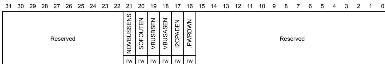
| 31 | 30 | 29 | 28 | 27 | 26 | 25 | 24 | 23 | 22 | 21 | 20 | 19 | 18 | 17 | 16 | 15 | 14 | 13 | 12 | 11 | 10 | 9 | 8 | 7 | 6 | 5 | 4 | 3 | 2 | 1 | 0 | ||||||
|---|---|---|---|---|---|---|---|---|---|---|---|---|---|---|---|---|---|---|---|---|---|---|---|---|---|---|---|---|---|---|---|---|---|---|---|---|---|
| Reserved | NOVBUSSENS | SOFOUTEN | VBUSBSEN | VBUSASEN | I2CPADEN | .PWRDWN | Reserved | ||||||||||||||||||||||||||||||
| rw | rw | rw | rw | rw | rw | ||||||||||||||||||||||||||||||||
Bits 31:22 Reserved, must be kept at reset value.
Bit 21 NOVBUSSENS : \( V_{BUS} \) sensing disable option
When this bit is set, \( V_{BUS} \) is considered internally to be always at \( V_{BUS} \) valid level (5 V). This option removes the need for a dedicated \( V_{BUS} \) pad, and leave this pad free to be used for other purposes such as a shared functionality. \( V_{BUS} \) connection can be remapped on another general purpose input pad and monitored by software.
This option is only suitable for host-only or device-only applications.
0: \( V_{BUS} \) sensing available by hardware
1: \( V_{BUS} \) sensing not available by hardware.
Bit 20 SOFOUTEN : SOF output enable
0: SOF pulse not available on PAD
1: SOF pulse available on PAD
Bit 19 VBUSBSEN : Enable the \( V_{BUS} \) sensing “B” device
0: \( V_{BUS} \) sensing “B” disabled
1: \( V_{BUS} \) sensing “B” enabled
Bit 18 VBUSASEN : Enable the \( V_{BUS} \) sensing “A” device
0: \( V_{BUS} \) sensing “A” disabled
1: \( V_{BUS} \) sensing “A” enabled
Bit 17 I2CPADEN : Enable \( I^2C \) bus connection for the external \( I^2C \) PHY interface.
0: \( I^2C \) bus disabled
1: \( I^2C \) bus enabled
Bit 16 PWRDWN : Power down
Used to activate the transceiver in transmission/reception
0: Power down active
1: Power down deactivated (“Transceiver active”)
Bits 15:0 Reserved, must be kept at reset value.
OTG_HS core ID register (OTG_HS_CID)
Address offset: 0x03C
Reset value: 0x0000 1100
This is a register containing the Product ID as reset value.
| 31 | 30 | 29 | 28 | 27 | 26 | 25 | 24 | 23 | 22 | 21 | 20 | 19 | 18 | 17 | 16 | 15 | 14 | 13 | 12 | 11 | 10 | 9 | 8 | 7 | 6 | 5 | 4 | 3 | 2 | 1 | 0 |
|---|---|---|---|---|---|---|---|---|---|---|---|---|---|---|---|---|---|---|---|---|---|---|---|---|---|---|---|---|---|---|---|
| PRODUCT_ID | |||||||||||||||||||||||||||||||
| rw | rw | rw | rw | rw | rw | rw | rw | rw | rw | rw | rw | rw | rw | rw | rw | rw | rw | rw | rw | rw | rw | rw | rw | rw | rw | rw | rw | rw | rw | rw | rw |
Bits 31:0 PRODUCT_ID : Product ID field
Application-programmable ID field.
OTG_HS Host periodic transmit FIFO size register (OTG_HS_HPTXFSIZ)
Address offset: 0x100
Reset value: 0x0200 0800

| 31 | 30 | 29 | 28 | 27 | 26 | 25 | 24 | 23 | 22 | 21 | 20 | 19 | 18 | 17 | 16 | 15 | 14 | 13 | 12 | 11 | 10 | 9 | 8 | 7 | 6 | 5 | 4 | 3 | 2 | 1 | 0 |
| PTXFD | PTXSA | ||||||||||||||||||||||||||||||
| r | r | r | r | r | r | r | r | r | r | r | r | r | r | r | r | r | r | r | r | r | r | r | r | r | r | r | r | r | r | r | r |
Bits 31:16 PTXFD : Host periodic TxFIFO depth
This value is in terms of 32-bit words.
Minimum value is 16
Maximum value is 512
Bits 15:0 PTXSA : Host periodic TxFIFO start address
The power-on reset value of this register is the sum of the largest Rx data FIFO depth and largest nonperiodic Tx data FIFO depth.
OTG_HS device IN endpoint transmit FIFO size register (OTG_HS_DIEPTXFx) (x = 1..5, where x is the FIFO_number)
Address offset: 0x104 + 0x04 * (x - 1)
Reset value: 0x02000400

| 31 | 30 | 29 | 28 | 27 | 26 | 25 | 24 | 23 | 22 | 21 | 20 | 19 | 18 | 17 | 16 | 15 | 14 | 13 | 12 | 11 | 10 | 9 | 8 | 7 | 6 | 5 | 4 | 3 | 2 | 1 | 0 |
| INEPTXFD | INEPTXSA | ||||||||||||||||||||||||||||||
| r | r | r | r | r | r | r | r | r | r | r | r | r | r | r | r | r | r | r | r | r | r | r | r | r | r | r | r | r | r | r | r |
Bits 31:16 INEPTXFD : IN endpoint TxFIFO depth
This value is in terms of 32-bit words.
Minimum value is 16
Maximum value is 512
The power-on reset value of this register is specified as the largest IN endpoint FIFO number depth.
Bits 15:0 INEPTXSA : IN endpoint FIFOx transmit RAM start address
This field contains the memory start address for IN endpoint transmit FIFOx. The address must be aligned with a 32-bit memory location.
35.12.3 Host-mode registers
Bit values in the register descriptions are expressed in binary unless otherwise specified.
Host-mode registers affect the operation of the core in the host mode. Host mode registers must not be accessed in peripheral mode, as the results are undefined. Host mode registers can be categorized as follows:
OTG_HS host configuration register (OTG_HS_HCFG)
Address offset: 0x400
Reset value: 0x0000 0000
This register configures the core after power-on. Do not change to this register after initializing the host.
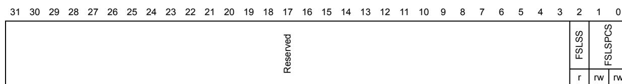
| 31 | 30 | 29 | 28 | 27 | 26 | 25 | 24 | 23 | 22 | 21 | 20 | 19 | 18 | 17 | 16 | 15 | 14 | 13 | 12 | 11 | 10 | 9 | 8 | 7 | 6 | 5 | 4 | 3 | 2 | 1 | 0 | |
| Reserved | FSLSS | FSLSPCS | ||||||||||||||||||||||||||||||
| r | rw | rw | ||||||||||||||||||||||||||||||
Bits 31:3 Reserved, must be kept at reset value.
Bit 2 FSLSS : FS- and LS-only support
The application uses this bit to control the core's enumeration speed. Using this bit, the application can make the core enumerate as an FS host, even if the connected device supports HS traffic. Do not make changes to this field after initial programming.
0: HS/FS/LS, based on the maximum speed supported by the connected device
1: FS/LS-only, even if the connected device can support HS (read-only)
Bits 1:0 FSLSPCS : FS/LS PHY clock select
When the core is in FS host mode:
01: PHY clock is running at 48 MHz
Others: Reserved
When the core is in LS host mode:
00: Reserved
01: PHY clock is running at 48 MHz.
10: Select 6 MHz PHY clock frequency
11: Reserved
Note: The FSLSPCS bit must be set on a connection event according to the speed of the connected device. A software reset must be performed after changing this bit.
OTG_HS Host frame interval register (OTG_HS_HFIR)
Address offset: 0x404
Reset value: 0x0000 EA60
This register stores the frame interval information for the current speed to which the OTG_HS controller has enumerated.

| 31 | 30 | 29 | 28 | 27 | 26 | 25 | 24 | 23 | 22 | 21 | 20 | 19 | 18 | 17 | 16 | 15 | 14 | 13 | 12 | 11 | 10 | 9 | 8 | 7 | 6 | 5 | 4 | 3 | 2 | 1 | 0 |
| Reserved | FRIVL | ||||||||||||||||||||||||||||||
| rw | rw | rw | rw | rw | rw | rw | rw | rw | rw | rw | rw | rw | rw | rw | rw | ||||||||||||||||
Bits 31:16 Reserved, must be kept at reset value.
Bits 15:0 FRIVL : Frame interval
The value that the application programs to this field specifies the interval between two consecutive SOFs (FS), micro-SOFs (HS) or Keep-Alive tokens (LS). This field contains the number of PHY clocks that constitute the required frame interval. The application can write a value to this register only after the Port enable bit of the host port control and status register (PENA bit in OTG_HS_HPRT) has been set. If no value is programmed, the core calculates the value based on the PHY clock specified in the FS/LS PHY Clock Select field of the Host configuration register (FSLSPCS in OTG_HS_HCFG):
frame duration × PHY clock frequency
- – Frame interval = 1 ms × (FRIVL - 1)
Note: The FRIVL bit can be modified whenever the application needs to change the Frame interval time.
OTG_HS host frame number/frame time remaining register (OTG_HS_HFNUM)
Address offset: 0x408
Reset value: 0x0000 3FFF
This register indicates the current frame number. It also indicates the time remaining (in terms of the number of PHY clocks) in the current frame.

| 31 | 30 | 29 | 28 | 27 | 26 | 25 | 24 | 23 | 22 | 21 | 20 | 19 | 18 | 17 | 16 | 15 | 14 | 13 | 12 | 11 | 10 | 9 | 8 | 7 | 6 | 5 | 4 | 3 | 2 | 1 | 0 |
| FTREM | FRNUM | ||||||||||||||||||||||||||||||
| r | r | r | r | r | r | r | r | r | r | r | r | r | r | r | r | r | r | r | r | r | r | r | r | r | r | r | r | r | r | r | r |
Bits 31:16 FTREM : Frame time remaining
Indicates the amount of time remaining in the current frame, in terms of PHY clocks. This field decrements on each PHY clock. When it reaches zero, this field is reloaded with the value in the Frame interval register and a new SOF is transmitted on the USB.
Bits 15:0 FRNUM : Frame number
This field increments when a new SOF is transmitted on the USB, and is cleared to 0 when it reaches 0x3FFF.
OTG_HS_Host periodic transmit FIFO/queue status register
(OTG_HS_HPTXSTS)
Address offset: 0x410
Reset value: 0x0008 0100
This read-only register contains the free space information for the periodic TxFIFO and the periodic transmit request queue.

| 31 | 30 | 29 | 28 | 27 | 26 | 25 | 24 | 23 | 22 | 21 | 20 | 19 | 18 | 17 | 16 | 15 | 14 | 13 | 12 | 11 | 10 | 9 | 8 | 7 | 6 | 5 | 4 | 3 | 2 | 1 | 0 |
| PTXQTOP | PTXQSAV | PTXFS AVL | |||||||||||||||||||||||||||||
| r | r | r | r | r | r | r | r | r | r | r | r | r | r | r | r | r | r | r | r | r | r | r | r | r | r | r | r | r | r | r | r |
Bits 31:24 PTXQTOP : Top of the periodic transmit request queue
This indicates the entry in the periodic Tx request queue that is currently being processed by the MAC.
This register is used for debugging.
Bit [31]: Odd/Even frame
- – 0: send in even (micro) frame
- – 1: send in odd (micro) frame
Bits [30:27]: Channel/endpoint number
Bits [26:25]: Type
- – 00: IN/OUT
- – 01: Zero-length packet
- – 11: Disable channel command
Bit [24]: Terminate (last entry for the selected channel/endpoint)
Bits 23:16 PTXQSAV : Periodic transmit request queue space available
Indicates the number of free locations available to be written in the periodic transmit request queue. This queue holds both IN and OUT requests.
00: Periodic transmit request queue is full
01: dx1 location available
10: dx2 locations available
bxn: dxn locations available ( \( 0 \leq dxn \leq PTXFD \) )
Others: Reserved
Bits 15:0 PTXFS AVL : Periodic transmit data FIFO space available
Indicates the number of free locations available to be written to in the periodic TxFIFO.
Values are in terms of 32-bit words
0000: Periodic TxFIFO is full
0001: dx1 word available
0010: dx2 words available
bxn: dxn words available (where \( 0 \leq dxn \leq dx512 \) )
Others: Reserved
OTG_HS Host all channels interrupt register (OTG_HS_HAINT)
Address offset: 0x414
Reset value: 0x0000 000
When a significant event occurs on a channel, the host all channels interrupt register interrupts the application using the host channels interrupt bit of the Core interrupt register (HCINT bit in OTG_HS_GINTSTS). This is shown in Figure 414 . There is one interrupt bit per channel, up to a maximum of 16 bits. Bits in this register are set and cleared when the application sets and clears bits in the corresponding host channel-x interrupt register.

| 31 | 30 | 29 | 28 | 27 | 26 | 25 | 24 | 23 | 22 | 21 | 20 | 19 | 18 | 17 | 16 | 15 | 14 | 13 | 12 | 11 | 10 | 9 | 8 | 7 | 6 | 5 | 4 | 3 | 2 | 1 | 0 |
| Reserved | HAINT | ||||||||||||||||||||||||||||||
| r | r | r | r | r | r | r | r | r | r | r | r | r | r | r | r | ||||||||||||||||
Bits 31:16 Reserved, must be kept at reset value.
Bits 15:0 HAINT : Channel interrupts
One bit per channel: Bit 0 for Channel 0, bit 15 for Channel 15
OTG_HS host all channels interrupt mask register (OTG_HS_HAINTMSK)
Address offset: 0x418
Reset value: 0x0000 0000
The host all channel interrupt mask register works with the host all channel interrupt register to interrupt the application when an event occurs on a channel. There is one interrupt mask bit per channel, up to a maximum of 16 bits.

| 31 | 30 | 29 | 28 | 27 | 26 | 25 | 24 | 23 | 22 | 21 | 20 | 19 | 18 | 17 | 16 | 15 | 14 | 13 | 12 | 11 | 10 | 9 | 8 | 7 | 6 | 5 | 4 | 3 | 2 | 1 | 0 |
| Reserved | HAINTM | ||||||||||||||||||||||||||||||
| rw | rw | rw | rw | rw | rw | rw | rw | rw | rw | rw | rw | rw | rw | rw | rw | ||||||||||||||||
Bits 31:16 Reserved, must be kept at reset value.
Bits 15:0 HAINTM : Channel interrupt mask
0: Masked interrupt
1: Unmasked interrupt
One bit per channel: Bit 0 for channel 0, bit 15 for channel 15
OTG_HS host port control and status register (OTG_HS_HPRT)
Address offset: 0x440
Reset value: 0x0000 0000
This register is available only in host mode. Currently, the OTG host supports only one port.
A single register holds USB port-related information such as USB reset, enable, suspend, resume, connect status, and test mode for each port. It is shown in Figure 414 . The rc_w1 bits in this register can trigger an interrupt to the application through the host port interrupt bit of the core interrupt register (HPRTINT bit in OTG_HS_GINTSTS). On a Port Interrupt, the application must read this register and clear the bit that caused the interrupt. For the rc_w1 bits, the application must write a 1 to the bit to clear the interrupt.
| 31 | 30 | 29 | 28 | 27 | 26 | 25 | 24 | 23 | 22 | 21 | 20 | 19 | 18 | 17 | 16 | 15 | 14 | 13 | 12 | 11 | 10 | 9 | 8 | 7 | 6 | 5 | 4 | 3 | 2 | 1 | 0 |
|---|---|---|---|---|---|---|---|---|---|---|---|---|---|---|---|---|---|---|---|---|---|---|---|---|---|---|---|---|---|---|---|
| Reserved | |||||||||||||||||||||||||||||||
Bits 31:19 Reserved, must be kept at reset value.
Bits 18:17 PSPD : Port speed
Indicates the speed of the device attached to this port.
- 00: High speed
- 01: Full speed
- 10: Low speed
- 11: Reserved
Bits 16:13 PTCTL : Port test control
The application writes a nonzero value to this field to put the port into a Test mode, and the corresponding pattern is signaled on the port.
- 0000: Test mode disabled
- 0001: Test_J mode
- 0010: Test_K mode
- 0011: Test_SE0_NAK mode
- 0100: Test_Packet mode
- 0101: Test_Force_Enable
- Others: Reserved
Bit 12 PPWR : Port power
The application uses this field to control power to this port, and the core clears this bit on an overcurrent condition.
- 0: Power off
- 1: Power on
Bits 11:10 PLSTS : Port line status
Indicates the current logic level USB data lines
- Bit [10]: Logic level of OTG_HS_FS_DP
- Bit [11]: Logic level of OTG_HS_FS_DM
Bit 9 Reserved, must be kept at reset value.
Bit 8 PRST: Port resetWhen the application sets this bit, a reset sequence is started on this port. The application must time the reset period and clear this bit after the reset sequence is complete.
0: Port not in reset
1: Port in reset
The application must leave this bit set for a minimum duration of at least 10 ms to start a reset on the port. The application can leave it set for another 10 ms in addition to the required minimum duration, before clearing the bit, even though there is no maximum limit set by the USB standard.
High speed: 50 ms
Full speed/Low speed: 10 ms
Bit 7 PSUSP: Port suspendThe application sets this bit to put this port in Suspend mode. The core only stops sending SOFs when this is set. To stop the PHY clock, the application must set the Port clock stop bit, which asserts the suspend input pin of the PHY.
The read value of this bit reflects the current suspend status of the port. This bit is cleared by the core after a remote wake-up signal is detected or the application sets the Port reset bit or Port resume bit in this register or the Resume/remote wake-up detected interrupt bit or Disconnect detected interrupt bit in the Core interrupt register (WKUINT or DISCINT in OTG_HS_GINTSTS, respectively).
0: Port not in Suspend mode
1: Port in Suspend mode
Bit 6 PRES: Port resumeThe application sets this bit to drive resume signaling on the port. The core continues to drive the resume signal until the application clears this bit.
If the core detects a USB remote wake-up sequence, as indicated by the Port resume/remote wake-up detected interrupt bit of the Core interrupt register (WKUINT bit in OTG_HS_GINTSTS), the core starts driving resume signaling without application intervention and clears this bit when it detects a disconnect condition. The read value of this bit indicates whether the core is currently driving resume signaling.
0: No resume driven
1: Resume driven
Bit 5 POCCHNG: Port overcurrent changeThe core sets this bit when the status of the Port overcurrent active bit (bit 4) in this register changes.
Bit 4 POCA: Port overcurrent activeIndicates the overcurrent condition of the port.
0: No overcurrent condition
1: Overcurrent condition
Bit 3 PENCHNG: Port enable/disable changeThe core sets this bit when the status of the Port enable bit [2] in this register changes.
Bit 2 PENA : Port enable
A port is enabled only by the core after a reset sequence, and is disabled by an overcurrent condition, a disconnect condition, or by the application clearing this bit. The application cannot set this bit by a register write. It can only clear it to disable the port. This bit does not trigger any interrupt to the application.
0: Port disabled
1: Port enabled
Bit 1 PCDET : Port connect detected
The core sets this bit when a device connection is detected to trigger an interrupt to the application using the host port interrupt bit in the Core interrupt register (HPRTINT bit in OTG_HS_GINTSTS). The application must write a 1 to this bit to clear the interrupt.
Bit 0 PCSTS : Port connect status
0: No device is attached to the port
1: A device is attached to the port
OTG_HS host channel-x characteristics register (OTG_HS_HCCHARx) (x = 0..11, where x = Channel_number)
Address offset: 0x500 + 0x20 * x
Reset value: 0x0000 0000
| 31 | 30 | 29 | 28 | 27 | 26 | 25 | 24 | 23 | 22 | 21 | 20 | 19 | 18 | 17 | 16 | 15 | 14 | 13 | 12 | 11 | 10 | 9 | 8 | 7 | 6 | 5 | 4 | 3 | 2 | 1 | 0 |
|---|---|---|---|---|---|---|---|---|---|---|---|---|---|---|---|---|---|---|---|---|---|---|---|---|---|---|---|---|---|---|---|
| CHENA | CHDIS | ODDFRM | DAD | MC | EPTYP | LSDEV | Reserved | EPDIR | EPNUM | MPSIZ | |||||||||||||||||||||
| rs | rs | rw | rw | rw | rw | rw | rw | rw | rw | rw | rw | rw | rw | rw | rw | rw | rw | rw | rw | rw | rw | rw | rw | rw | rw | rw | rw | rw | rw | rw | |
Bit 31 CHENA : Channel enable
This field is set by the application and cleared by the OTG host.
0: Channel disabled
1: Channel enabled
Bit 30 CHDIS : Channel disable
The application sets this bit to stop transmitting/receiving data on a channel, even before the transfer for that channel is complete. The application must wait for the Channel disabled interrupt before treating the channel as disabled.
Bit 29 ODDFRM : Odd frame
This field is set (reset) by the application to indicate that the OTG host must perform a transfer in an odd frame. This field is applicable for only periodic (isochronous and interrupt) transactions.
0: Even (micro) frame
1: Odd (micro) frame
Bits 28:22 DAD : Device address
This field selects the specific device serving as the data source or sink.
Bits 21:20 MC : Multi Count (MC) / Error Count (EC)
- – When the split enable bit (SPLITEN) in the host channel-x split control register (OTG_HS_HCSPLTx) is reset (0), this field indicates to the host the number of transactions that must be executed per micro-frame for this periodic endpoint. For nonperiodic transfers, this field specifies the number of packets to be fetched for this channel before the internal DMA engine changes arbitration.
- 00: Reserved This field yields undefined results
- 01: 1 transaction
- b10: 2 transactions to be issued for this endpoint per micro-frame
- 11: 3 transactions to be issued for this endpoint per micro-frame.
- – When the SPLITEN bit is set (1) in OTG_HS_HCSPLTx, this field indicates the number of immediate retries to be performed for a periodic split transaction on transaction errors. This field must be set to at least 01.
Bits 19:18 EPTYP : Endpoint type
Indicates the transfer type selected.
- 00: Control
- 01: Isochronous
- 10: Bulk
- 11: Interrupt
Bit 17 LSDEV : Low-speed device
This field is set by the application to indicate that this channel is communicating to a low-speed device.
Bit 16 Reserved, must be kept at reset value.
Bit 15 EPDIR : Endpoint direction
Indicates whether the transaction is IN or OUT.
- 0: OUT
- 1: IN
Bits 14:11 EPNUM : Endpoint number
Indicates the endpoint number on the device serving as the data source or sink.
Bits 10:0 MPSIZ : Maximum packet size
Indicates the maximum packet size of the associated endpoint.
OTG_HS host channel-x split control register (OTG_HS_HCSPLTx) (x = 0..11, where x = Channel_number)
Address offset: 0x504 + 0x20 * x
Reset value: 0x0000 0000
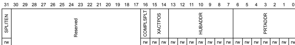
| 31 | 30 | 29 | 28 | 27 | 26 | 25 | 24 | 23 | 22 | 21 | 20 | 19 | 18 | 17 | 16 | 15 | 14 | 13 | 12 | 11 | 10 | 9 | 8 | 7 | 6 | 5 | 4 | 3 | 2 | 1 | 0 | ||||
| SPLITEN | Reserved | COMPLSPLIT | XACTPOS | HUBADDR | PRTADDR | ||||||||||||||||||||||||||||||
| rw | rw | rw | rw | rw | rw | rw | rw | rw | rw | rw | rw | rw | rw | rw | rw | rw | rw | rw | rw | rw | |||||||||||||||
Bit 31 SPLITEN : Split enable
The application sets this bit to indicate that this channel is enabled to perform split transactions.
Bits 30:17 Reserved, must be kept at reset value.
Bit 16 COMPLSPLIT : Do complete split
The application sets this bit to request the OTG host to perform a complete split transaction.
Bits 15:14 XACTPOS : Transaction position
This field is used to determine whether to send all, first, middle, or last payloads with each OUT transaction.
11: All. This is the entire data payload of this transaction (which is less than or equal to 188 bytes)
10: Begin. This is the first data payload of this transaction (which is larger than 188 bytes)
00: Mid. This is the middle payload of this transaction (which is larger than 188 bytes)
01: End. This is the last payload of this transaction (which is larger than 188 bytes)
Bits 13:7 HUBADDR : Hub address
This field holds the device address of the transaction translator's hub.
Bits 6:0 PRTADDR : Port address
This field is the port number of the recipient transaction translator.
OTG_HS host channel-x interrupt register (OTG_HS_HCINTx) (x = 0..11, where x = Channel_number)
Address offset: 0x508 + 0x20 * x
Reset value: 0x0000 0000
This register indicates the status of a channel with respect to USB- and AHB-related events. It is shown in Figure 414 . The application must read this register when the host channels interrupt bit in the Core interrupt register (HCINT bit in OTG_HS_GINTSTS) is set. Before the application can read this register, it must first read the host all channels interrupt (OTG_HS_HAINT) register to get the exact channel number for the host channel-x interrupt register. The application must clear the appropriate bit in this register to clear the corresponding bits in the OTG_HS_HAINT and OTG_HS_GINTSTS registers.
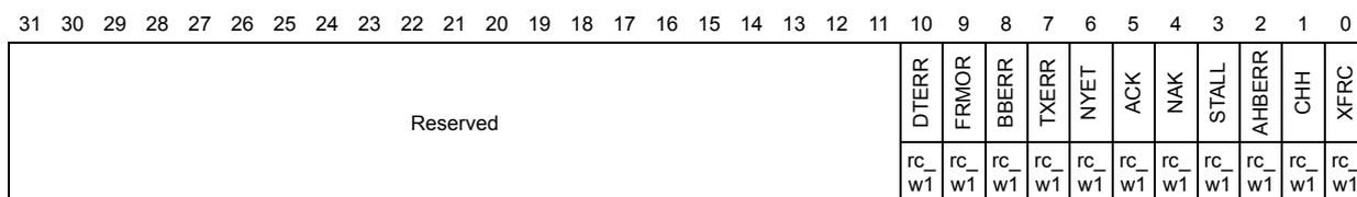
| 31 | 30 | 29 | 28 | 27 | 26 | 25 | 24 | 23 | 22 | 21 | 20 | 19 | 18 | 17 | 16 | 15 | 14 | 13 | 12 | 11 | 10 | 9 | 8 | 7 | 6 | 5 | 4 | 3 | 2 | 1 | 0 |
| Reserved | DTERR | FRMOR | BBERR | TXERR | NYET | ACK | NAK | STALL | AHBERR | CHH | XFRC | ||||||||||||||||||||
| rc_w1 | rc_w1 | rc_w1 | rc_w1 | rc_w1 | rc_w1 | rc_w1 | rc_w1 | rc_w1 | rc_w1 | rc_w1 | |||||||||||||||||||||
Bits 31:11 Reserved, must be kept at reset value.
Bit 10 DTERR : Data toggle error
Bit 9 FRMOR : Frame overrun
Bit 8 BBERR : Babble error
Bit 7 TXERR : Transaction error
Indicates one of the following errors occurred on the USB.
CRC check failure
Timeout
Bit stuff error
False EOP
Bit 6 NYET : Response received interrupt
Bit 5 ACK : ACK response received/transmitted interrupt
Bit 4 NAK : NAK response received interrupt
Bit 3 STALL : STALL response received interrupt
Bit 2 AHBERR : AHB error
This error is generated only in Internal DMA mode when an AHB error occurs during an AHB read/write operation. The application can read the corresponding DMA channel address register to get the error address.
Bit 1 CHH : Channel halted
Indicates the transfer completed abnormally either because of any USB transaction error or in response to disable request by the application.
Bit 0 XFRC : Transfer completed
Transfer completed normally without any errors.
OTG_HS host channel-x interrupt mask register (OTG_HS_HCINTMSKx)
(x = 0..11, where x = Channel_number)
Address offset: 0x50C + 0x20 * x
Reset value: 0x0000 0000
This register reflects the mask for each channel status described in the previous section.
| 31 | 30 | 29 | 28 | 27 | 26 | 25 | 24 | 23 | 22 | 21 | 20 | 19 | 18 | 17 | 16 | 15 | 14 | 13 | 12 | 11 | 10 | 9 | 8 | 7 | 6 | 5 | 4 | 3 | 2 | 1 | 0 |
|---|---|---|---|---|---|---|---|---|---|---|---|---|---|---|---|---|---|---|---|---|---|---|---|---|---|---|---|---|---|---|---|
| Reserved | DTERRM | FRMORM | BBERRM | TXERRM | NYET | ACKM | NAKM | STALLM | AHBERRM | CHHM | XFRM | ||||||||||||||||||||
| rw | rw | rw | rw | rw | rw | rw | rw | rw | rw | rw | |||||||||||||||||||||
Bits 31:11 Reserved, must be kept at reset value.
Bit 10 DTERRM : Data toggle error mask
- 0: Masked interrupt
- 1: Unmasked interrupt
Bit 9 FRMORM : Frame overrun mask
- 0: Masked interrupt
- 1: Unmasked interrupt
Bit 8 BBERRM : Babble error mask
- 0: Masked interrupt
- 1: Unmasked interrupt
Bit 7 TXERRM : Transaction error mask
- 0: Masked interrupt
- 1: Unmasked interrupt
Bit 6 NYET : response received interrupt mask
- 0: Masked interrupt
- 1: Unmasked interrupt
Bit 5 ACKM : ACK response received/transmitted interrupt mask
- 0: Masked interrupt
- 1: Unmasked interrupt
Bit 4 NAKM : NAK response received interrupt mask
- 0: Masked interrupt
- 1: Unmasked interrupt
Bit 3 STALLM : STALL response received interrupt mask
- 0: Masked interrupt
- 1: Unmasked interrupt
Bit 2 AHBERRM : AHB error mask
0: Masked interrupt
1: Unmasked interrupt
Bit 1 CHHM : Channel halted mask
0: Masked interrupt
1: Unmasked interrupt
Bit 0 XFRCM : Transfer completed mask
0: Masked interrupt
1: Unmasked interrupt
OTG_HS host channel-x transfer size register (OTG_HS_HCTSIZx) (x = 0..11, where x = Channel_number)
Address offset: 0x510 + 0x20 * x
Reset value: 0x0000 0000
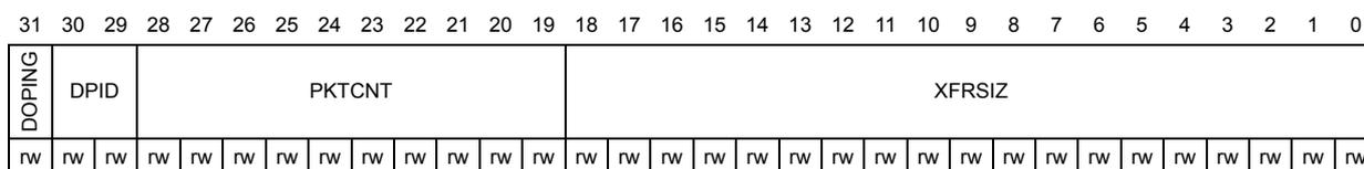
| 31 | 30 | 29 | 28 | 27 | 26 | 25 | 24 | 23 | 22 | 21 | 20 | 19 | 18 | 17 | 16 | 15 | 14 | 13 | 12 | 11 | 10 | 9 | 8 | 7 | 6 | 5 | 4 | 3 | 2 | 1 | 0 |
| DOPING | DPID | PKTCNT | XFRSIZ | ||||||||||||||||||||||||||||
| rw | rw | rw | rw | rw | rw | rw | rw | rw | rw | rw | rw | rw | rw | rw | rw | rw | rw | rw | rw | rw | rw | rw | rw | rw | rw | rw | rw | rw | rw | rw | rw |
Bit 31 DOPING : Do ping
This bit is used only for OUT transfers. Setting this field to 1 directs the host to do PING protocol.
Note: Do not set this bit for IN transfers. If this bit is set for IN transfers it disables the channel.
Bits 30:29 DPID : Data PID
The application programs this field with the type of PID to use for the initial transaction. The host maintains this field for the rest of the transfer.
00: DATA0
01: DATA2
10: DATA1
11: MDATA (noncontrol)/SETUP (control)
Bits 28:19 PKTCNT : Packet count
This field is programmed by the application with the expected number of packets to be transmitted (OUT) or received (IN).
The host decrements this count on every successful transmission or reception of an OUT/IN packet. Once this count reaches zero, the application is interrupted to indicate normal completion.
Bits 18:0 XFRSIZ : Transfer size
For an OUT, this field is the number of data bytes the host sends during the transfer.
For an IN, this field is the buffer size that the application has reserved for the transfer. The application is expected to program this field as an integer multiple of the maximum packet size for IN transactions (periodic and nonperiodic).
OTG_HS host channel-x DMA address register (OTG_HS_HCDMAx) (x = 0..11, where x = Channel_number)
Address offset: \( 0x514 + 0x20 * x \)
Reset value: 0x0000 0000

| 31 | 30 | 29 | 28 | 27 | 26 | 25 | 24 | 23 | 22 | 21 | 20 | 19 | 18 | 17 | 16 | 15 | 14 | 13 | 12 | 11 | 10 | 9 | 8 | 7 | 6 | 5 | 4 | 3 | 2 | 1 | 0 |
| DMAADDR | |||||||||||||||||||||||||||||||
| rw | rw | rw | rw | rw | rw | rw | rw | rw | rw | rw | rw | rw | rw | rw | rw | rw | rw | rw | rw | rw | rw | rw | rw | rw | rw | rw | rw | rw | rw | rw | rw |
Bits 31:0 DMAADDR : DMA address
This field holds the start address in the external memory from which the data for the endpoint must be fetched or to which it must be stored. This register is incremented on every AHB transaction.
35.12.4 Device-mode registers
OTG_HS device configuration register (OTG_HS_DCFG)
Address offset: 0x800
Reset value: 0x0220 0000
This register configures the core in peripheral mode after power-on or after certain control commands or enumeration. Do not make changes to this register after initial programming.
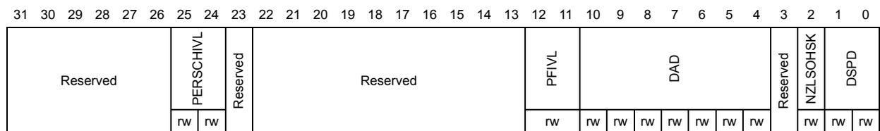
| 31 | 30 | 29 | 28 | 27 | 26 | 25 | 24 | 23 | 22 | 21 | 20 | 19 | 18 | 17 | 16 | 15 | 14 | 13 | 12 | 11 | 10 | 9 | 8 | 7 | 6 | 5 | 4 | 3 | 2 | 1 | 0 |
| Reserved | PERSCHIVL | Reserved | Reserved | PFIVL | DAD | Reserved | NZLSOHSK | DSPD | |||||||||||||||||||||||
| rw | rw | rw | rw | rw | rw | rw | rw | rw | rw | rw | rw | rw | |||||||||||||||||||
Bits 31:26 Reserved, must be kept at reset value.
Bits 25:24 PERSCHIVL : Periodic scheduling interval
This field specifies the amount of time the Internal DMA engine must allocate for fetching periodic IN endpoint data. Based on the number of periodic endpoints, this value must be specified as 25, 50 or 75% of the (micro)frame.
- – When any periodic endpoints are active, the internal DMA engine allocates the specified amount of time in fetching periodic IN endpoint data
- – When no periodic endpoint is active, then the internal DMA engine services nonperiodic endpoints, ignoring this field
- – After the specified time within a (micro)frame, the DMA switches to fetching nonperiodic endpoints
00: 25% of (micro)frame
01: 50% of (micro)frame
10: 75% of (micro)frame
11: Reserved
Bits 23:13 Reserved, must be kept at reset value.
Bits 12:11 PFIVL : Periodic (micro)frame intervalIndicates the time within a (micro) frame at which the application must be notified using the end of periodic (micro) frame interrupt. This can be used to determine if all the isochronous traffic for that frame is complete.
00: 80% of the frame interval
01: 85% of the frame interval
10: 90% of the frame interval
11: 95% of the frame interval
Bits 10:4 DAD : Device addressThe application must program this field after every SetAddress control command.
Bit 3 Reserved, must be kept at reset value.
Bit 2 NZLSOHSK : Nonzero-length status OUT handshakeThe application can use this field to select the handshake the core sends on receiving a nonzero-length data packet during the OUT transaction of a control transfer's Status stage.
1: Send a STALL handshake on a nonzero-length status OUT transaction and do not send the received OUT packet to the application.
0: Send the received OUT packet to the application (zero-length or nonzero-length) and send a handshake based on the NAK and STALL bits for the endpoint in the device endpoint control register.
Bits 1:0 DSPD : Device speedIndicates the speed at which the application requires the core to enumerate, or the maximum speed the application can support. However, the actual bus speed is determined only after the chirp sequence is completed, and is based on the speed of the USB host to which the core is connected.
00: High speed
01: Full speed using external ULPI PHY
10: Reserved
11: Full speed using internal embedded PHY
OTG_HS device control register (OTG_HS_DCTL)
Address offset: 0x804
Reset value: 0x0000 0000
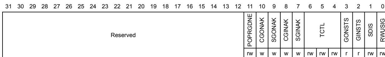
| 31 | 30 | 29 | 28 | 27 | 26 | 25 | 24 | 23 | 22 | 21 | 20 | 19 | 18 | 17 | 16 | 15 | 14 | 13 | 12 | 11 | 10 | 9 | 8 | 7 | 6 | 5 | 4 | 3 | 2 | 1 | 0 |
| Reserved | POPRGDNE | CGONAK | SGONAK | CGINAK | SGINAK | TCTL | GONSTS | GINSTS | SDIS | RWUSIG | |||||||||||||||||||||
| rw | w | w | w | w | rw | rw | rw | r | r | rw | rw | ||||||||||||||||||||
Bits 31:12 Reserved, must be kept at reset value.
Bit 11 POPRGDNE : Power-on programming done
The application uses this bit to indicate that register programming is completed after a wake-up from power down mode.
Bit 10 CGONAK : Clear global OUT NAK
Writing 1 to this field clears the Global OUT NAK.
Bit 9 SGONAK : Set global OUT NAK
Writing 1 to this field sets the Global OUT NAK.
The application uses this bit to send a NAK handshake on all OUT endpoints.
The application must set this bit only after making sure that the Global OUT NAK effective bit in the Core interrupt register (GONAKEFF bit in OTG_HS_GINTSTS) is cleared.
Bit 8 CGINAK : Clear global IN NAK
Writing 1 to this field clears the Global IN NAK.
Bit 7 SGINAK : Set global IN NAK
Writing 1 to this field sets the Global nonperiodic IN NAK. The application uses this bit to send a NAK handshake on all nonperiodic IN endpoints.
The application must set this bit only after making sure that the Global IN NAK effective bit in the Core interrupt register (GINAKEFF bit in OTG_HS_GINTSTS) is cleared.
Bits 6:4 TCTL : Test control
- 000: Test mode disabled
- 001: Test_J mode
- 010: Test_K mode
- 011: Test_SE0_NAK mode
- 100: Test_Packet mode
- 101: Test_Force_Enable
- Others: Reserved
Bit 3 GONSTS : Global OUT NAK status
- 0: A handshake is sent based on the FIFO Status and the NAK and STALL bit settings.
- 1: No data is written to the RxFIFO, irrespective of space availability. Sends a NAK handshake on all packets, except on SETUP transactions. All isochronous OUT packets are dropped.
Bit 2 GINSTS : Global IN NAK status
0: A handshake is sent out based on the data availability in the transmit FIFO.
1: A NAK handshake is sent out on all nonperiodic IN endpoints, irrespective of the data availability in the transmit FIFO.
Bit 1 SDIS : Soft disconnect
The application uses this bit to signal the USB OTG core to perform a soft disconnect. As long as this bit is set, the host does not see that the device is connected, and the device does not receive signals on the USB. The core stays in the disconnected state until the application clears this bit.
0: Normal operation. When this bit is cleared after a soft disconnect, the core generates a device connect event to the USB host. When the device is reconnected, the USB host restarts device enumeration.
1: The core generates a device disconnect event to the USB host.
Bit 0 RWUSIG : Remote wake-up signaling
When the application sets this bit, the core initiates remote signaling to wake up the USB host. The application must set this bit to instruct the core to exit the Suspend state. As specified in the USB 2.0 specification, the application must clear this bit 1 ms to 15 ms after setting it.
Table 215 contains the minimum duration (according to device state) for which the Soft disconnect (SDIS) bit must be set for the USB host to detect a device disconnect. To accommodate clock jitter, it is recommended that the application add some extra delay to the specified minimum duration.
Table 215. Minimum duration for soft disconnect
| Operating speed | Device state | Minimum duration |
|---|---|---|
| High speed | Not Idle or Suspended (Performing transactions) | 125 µs |
| Full speed | Suspended | 1 ms + 2.5 µs |
| Full speed | Idle | 2.5 µs |
| Full speed | Not Idle or Suspended (Performing transactions) | 2.5 µs |
OTG_HS device status register (OTG_HS_DSTS)
Address offset: 0x808
Reset value: 0x0000 0010
This register indicates the status of the core with respect to USB-related events. It must be read on interrupts from the device all interrupts (OTG_HS_DAININT) register.
| 31 | 30 | 29 | 28 | 27 | 26 | 25 | 24 | 23 | 22 | 21 | 20 | 19 | 18 | 17 | 16 | 15 | 14 | 13 | 12 | 11 | 10 | 9 | 8 | 7 | 6 | 5 | 4 | 3 | 2 | 1 | 0 |
| Reserved | FNSOF | Reserved | EERR | ENUMSPD | SUSPSTS | ||||||||||||||||||||||||||
| r | r | r | r | r | r | r | r | r | r | r | r | r | r | r | r | r | r | r | r | r | r | r | r | ||||||||
Bits 31:22 Reserved, must be kept at reset value.
Bits 21:8 FNSOF : Frame number of the received SOF
Bits 7:4 Reserved, must be kept at reset value.
Bit 3 EERR : Erratic error
The core sets this bit to report any erratic errors.
Due to erratic errors, the OTG_HS controller goes into Suspended state and an interrupt is generated to the application with Early suspend bit of the Core interrupt register (ESUSP bit in OTG_HS_GINTSTS). If the early suspend is asserted due to an erratic error, the application can only perform a soft disconnect/recover.
Bits 2:1 ENUMSPD : Enumerated speed
Indicates the speed at which the OTG_HS controller has come up after speed detection through a chirp sequence.
00: High speed
01: Reserved
10: Reserved
11: Full speed (PHY clock is running at 48 MHz)
Others: reserved
Bit 0 SUSPSTS : Suspend status
In peripheral mode, this bit is set as long as a Suspend condition is detected on the USB.
The core enters the Suspended state when there is no activity on the USB data lines for a period of 3 ms. The core comes out of the suspend:
- – When there is an activity on the USB data lines
- – When the application writes to the Remote wake-up signaling bit in the Device control register (RWUSIG bit in OTG_HS_DCTL).
OTG_HS device IN endpoint common interrupt mask register (OTG_HS_DIEPMSK)
Address offset: 0x810
Reset value: 0x0000 0000
This register works with each of the Device IN endpoint interrupt (OTG_HS_DIEPINTx) registers for all endpoints to generate an interrupt per IN endpoint. The IN endpoint interrupt for a specific status in the OTG_HS_DIEPINTx register can be masked by writing to the corresponding bit in this register. Status bits are masked by default.
| 31 | 30 | 29 | 28 | 27 | 26 | 25 | 24 | 23 | 22 | 21 | 20 | 19 | 18 | 17 | 16 | 15 | 14 | 13 | 12 | 11 | 10 | 9 | 8 | 7 | 6 | 5 | 4 | 3 | 2 | 1 | 0 |
| Reserved | NAKM | Reserved | TXFURM | Reserved | INEPNEM | INEPNMM | ITTXFEMSK | TOM | AHBERRM | EPDM | XFRCM | ||||||||||||||||||||
| rw | rw | rw | rw | rw | rw | rw | rw | rw | |||||||||||||||||||||||
Bits 31:14 Reserved, must be kept at reset value.
Bit 13
NAKM
: NAK interrupt mask
0: Masked interrupt
1: Unmasked interrupt
Bits 12:9 Reserved, must be kept at reset value.
Bit 8
TXFURM
: FIFO underrun mask
0: Masked interrupt
1: Unmasked interrupt
Bit 7 Reserved, must be kept at reset value.
Bit 6
INEPNEM
: IN endpoint NAK effective mask
0: Masked interrupt
1: Unmasked interrupt
Bit 5
INEPNMM
: IN token received with EP mismatch mask
0: Masked interrupt
1: Unmasked interrupt
Bit 4
ITTXFEMSK
: IN token received when TxFIFO empty mask
0: Masked interrupt
1: Unmasked interrupt
Bit 3
TOM
: Timeout condition mask (nonisochronous endpoints)
0: Masked interrupt
1: Unmasked interrupt
Bit 2 AHBERRM : AHB error mask
0: Masked interrupt
1: Unmasked interrupt
Bit 1 EPDM : Endpoint disabled interrupt mask
0: Masked interrupt
1: Unmasked interrupt
Bit 0 XFRCM : Transfer completed interrupt mask
0: Masked interrupt
1: Unmasked interrupt
OTG_HS device OUT endpoint common interrupt mask register (OTG_HS_DOEPMSK)
Address offset: 0x814
Reset value: 0x0000 0000
This register works with each of the Device OUT endpoint interrupt (OTG_HS_DOEPINTx) registers for all endpoints to generate an interrupt per OUT endpoint. The OUT endpoint interrupt for a specific status in the OTG_HS_DOEPINTx register can be masked by writing into the corresponding bit in this register. Status bits are masked by default.
| 31 | 30 | 29 | 28 | 27 | 26 | 25 | 24 | 23 | 22 | 21 | 20 | 19 | 18 | 17 | 16 | 15 | 14 | 13 | 12 | 11 | 10 | 9 | 8 | 7 | 6 | 5 | 4 | 3 | 2 | 1 | 0 |
|---|---|---|---|---|---|---|---|---|---|---|---|---|---|---|---|---|---|---|---|---|---|---|---|---|---|---|---|---|---|---|---|
| Reserved | NYETMSK | NAKMSK | BERRM | Reserved | OPEM | Reserved | B2BSTUP | STSPHSRXM | OTEPDM | STUPM | AHBERRM | EPDM | XFRCM | ||||||||||||||||||
| rw | rw | rw | rw | rw | rw | rw | rw | rw | rw | ||||||||||||||||||||||
Bits 31:15 Reserved, must be kept at reset value.
Bit 14 NYETMSK : NYET interrupt mask
0: Masked interrupt
1: Unmasked interrupt
Bit 13 NAKMSK : NAK interrupt mask
0: Masked interrupt
1: Unmasked interrupt
Bit 12 BERRM : Babble error interrupt mask
0: Masked interrupt
1: Unmasked interrupt
Bits 11:9 Reserved, must be kept at reset value.
Bit 8 OPEM : OUT packet error mask
0: Masked interrupt
1: Unmasked interrupt
Bit 7 Reserved, must be kept at reset value.
- Bit 6
B2BSTUP
: Back-to-back SETUP packets received mask
Applies to control OUT endpoints only.
0: Masked interrupt
1: Unmasked interrupt - Bit 5
STSPHSRXM
: Status phase received for control write mask
0: Masked interrupt
1: Unmasked interrupt - Bit 4
OTEPDM
: OUT token received when endpoint disabled mask
Applies to control OUT endpoints only.
0: Masked interrupt
1: Unmasked interrupt - Bit 3
STUPM
: SETUP phase done mask
Applies to control endpoints only.
0: Masked interrupt
1: Unmasked interrupt - Bit 2
AHBERRM
: AHB error mask
0: Masked interrupt
1: Unmasked interrupt - Bit 1
EPDM
: Endpoint disabled interrupt mask
0: Masked interrupt
1: Unmasked interrupt - Bit 0
XFRCM
: Transfer completed interrupt mask
0: Masked interrupt
1: Unmasked interrupt
OTG_HS device all endpoints interrupt register (OTG_HS_DAINT)
Address offset: 0x818
Reset value: 0x0000 0000
When a significant event occurs on an endpoint, a device all endpoints interrupt register interrupts the application using the Device OUT endpoints interrupt bit or Device IN endpoints interrupt bit of the Core interrupt register (OEPINT or IEPINT in OTG_HS_GINTSTS, respectively). There is one interrupt bit per endpoint, up to a maximum of 16 bits for OUT endpoints and 16 bits for IN endpoints. For a bidirectional endpoint, the corresponding IN and OUT interrupt bits are used. Bits in this register are set and cleared when the application sets and clears bits in the corresponding Device Endpoint-x interrupt register (OTG_HS_DIEPINTx/OTG_HS_DOEPINTx).

| 31 | 30 | 29 | 28 | 27 | 26 | 25 | 24 | 23 | 22 | 21 | 20 | 19 | 18 | 17 | 16 | 15 | 14 | 13 | 12 | 11 | 10 | 9 | 8 | 7 | 6 | 5 | 4 | 3 | 2 | 1 | 0 |
| OEPINT | IEPINT | ||||||||||||||||||||||||||||||
| r | r | r | r | r | r | r | r | r | r | r | r | r | r | r | r | r | r | r | r | r | r | r | r | r | r | r | r | r | r | r | r |
Bits 31:16 OEPINT : OUT endpoint interrupt bits
One bit per OUT endpoint:
Bit 16 for OUT endpoint 0, bit 31 for OUT endpoint 15
Bits 15:0 IEPINT : IN endpoint interrupt bits
One bit per IN endpoint:
Bit 0 for IN endpoint 0, bit 15 for endpoint 15
OTG_HS all endpoints interrupt mask register (OTG_HS_DAINTMSK)
Address offset: 0x81C
Reset value: 0x0000 0000
The device endpoint interrupt mask register works with the device endpoint interrupt register to interrupt the application when an event occurs on a device endpoint. However, the device all endpoints interrupt (OTG_HS_DAINT) register bit corresponding to that interrupt is still set.

| 31 | 30 | 29 | 28 | 27 | 26 | 25 | 24 | 23 | 22 | 21 | 20 | 19 | 18 | 17 | 16 | 15 | 14 | 13 | 12 | 11 | 10 | 9 | 8 | 7 | 6 | 5 | 4 | 3 | 2 | 1 | 0 |
| OEPM | IEPM | ||||||||||||||||||||||||||||||
| rw | rw | rw | rw | rw | rw | rw | rw | rw | rw | rw | rw | rw | rw | rw | rw | rw | rw | rw | rw | rw | rw | rw | rw | rw | rw | rw | rw | rw | rw | rw | rw |
Bits 31:16 OEPM : OUT EP interrupt mask bits
- One per OUT endpoint:
- Bit 16 for OUT EP 0, bit 19 for OUT EP 3
- 0: Masked interrupt
- 1: Unmasked interrupt
Bits 15:0 IEPM : IN EP interrupt mask bits
- One bit per IN endpoint:
- Bit 0 for IN EP 0, bit 3 for IN EP 3
- 0: Masked interrupt
- 1: Unmasked interrupt
OTG_HS device V BUS discharge time register (OTG_HS_DVBUSDIS)
Address offset: 0x0828
Reset value: 0x0000 17D7
This register specifies the V BUS discharge time after V BUS pulsing during SRP.

| 31 | 30 | 29 | 28 | 27 | 26 | 25 | 24 | 23 | 22 | 21 | 20 | 19 | 18 | 17 | 16 | 15 | 14 | 13 | 12 | 11 | 10 | 9 | 8 | 7 | 6 | 5 | 4 | 3 | 2 | 1 | 0 |
| Reserved | VBUSDT | ||||||||||||||||||||||||||||||
| rw | rw | rw | rw | rw | rw | rw | rw | rw | rw | rw | rw | rw | rw | rw | rw | ||||||||||||||||
Bits 31:16 Reserved, must be kept at reset value.
Bits 15:0 VBUSDT : Device V BUS discharge time
Specifies the V
BUS
discharge time after V
BUS
pulsing during SRP. This value equals:
V
BUS
discharge time in PHY clocks / 1 024
Depending on your V
BUS
load, this value may need adjusting.
Address offset: 0x082C
Reset value: 0x0000 05B8
This register specifies the V BUS pulsing time during SRP.
| 31 | 30 | 29 | 28 | 27 | 26 | 25 | 24 | 23 | 22 | 21 | 20 | 19 | 18 | 17 | 16 | 15 | 14 | 13 | 12 | 11 | 10 | 9 | 8 | 7 | 6 | 5 | 4 | 3 | 2 | 1 | 0 |
| Reserved | DVBUSP | ||||||||||||||||||||||||||||||
| rw | rw | rw | rw | rw | rw | rw | rw | rw | rw | rw | rw | ||||||||||||||||||||
Bits 31:12 Reserved, must be kept at reset value.
Bits 11:0 DVBUSP : Device V BUS pulsing timeSpecifies the V BUS pulsing time during SRP. This value equals:V BUS pulsing time in PHY clocks / 1 024OTG_HS Device threshold control register (OTG_HS_DTHRCTL)
Address offset: 0x0830
Reset value: 0x0000 0000
| 31 | 30 | 29 | 28 | 27 | 26 | 25 | 24 | 23 | 22 | 21 | 20 | 19 | 18 | 17 | 16 | 15 | 14 | 13 | 12 | 11 | 10 | 9 | 8 | 7 | 6 | 5 | 4 | 3 | 2 | 1 | 0 | |
| Reserved | ARPEN | Reserved | RXTHRELEN | RXTHREN | Reserved | TXTHRELEN | ISOTHREN | NONISOTHREN | ||||||||||||||||||||||||
| rw | rw | rw | rw | rw | rw | rw | rw | rw | rw | rw | rw | rw | rw | rw | rw | rw | rw | rw | rw | rw | rw | |||||||||||
Bits 31:28 Reserved, must be kept at reset value.
Bit 27 ARPEN : Arbiter parking enable
This bit controls internal DMA arbiter parking for IN endpoints. When thresholding is enabled and this bit is set to one, then the arbiter parks on the IN endpoint for which there is a token received on the USB. This is done to avoid getting into underrun conditions. By default parking is enabled.
Bit 26 Reserved, must be kept at reset value.
Bits 25: 17 RXTHRELEN : Receive threshold length
This field specifies the receive thresholding size in words. This field also specifies the amount of data received on the USB before the core can start transmitting on the AHB. The threshold length has to be at least eight words. The recommended value for RXTHRELEN is to be the same as the programmed AHB burst length (HBSTLEN bit in OTG_HS_GAHBCFG).
Bit 16 RXTHREN : Receive threshold enable
When this bit is set, the core enables thresholding in the receive direction.
Bits 15: 11 Reserved, must be kept at reset value.
Bits 10:2 TXTHRELEN : Transmit threshold length
This field specifies the transmit thresholding size in words. This field specifies the amount of data in bytes to be in the corresponding endpoint transmit FIFO, before the core can start transmitting on the USB. The threshold length has to be at least eight words. This field controls both isochronous and nonisochronous IN endpoint thresholds. The recommended value for TXTHRELEN is to be the same as the programmed AHB burst length (HBSTLEN bit in OTG_HS_GAHBCFG).
Bit 1 ISOTHREN : ISO IN endpoint threshold enable
When this bit is set, the core enables thresholding for isochronous IN endpoints.
Bit 0 NONISOTHREN : Nonisochronous IN endpoints threshold enable
When this bit is set, the core enables thresholding for nonisochronous IN endpoints.
OTG_HS device IN endpoint FIFO empty interrupt mask register:
(OTG_HS_DIEPEMPMSK)
Address offset: 0x834
Reset value: 0x0000 0000
This register is used to control the IN endpoint FIFO empty interrupt generation (TXFE_OTG_HS_DIEPINTx).

| 31 | 30 | 29 | 28 | 27 | 26 | 25 | 24 | 23 | 22 | 21 | 20 | 19 | 18 | 17 | 16 | 15 | 14 | 13 | 12 | 11 | 10 | 9 | 8 | 7 | 6 | 5 | 4 | 3 | 2 | 1 | 0 |
| Reserved | INEPTXFEM | ||||||||||||||||||||||||||||||
| rw | rw | rw | rw | rw | rw | rw | rw | rw | rw | rw | rw | rw | rw | rw | rw | rw | rw | rw | rw | ||||||||||||
Bits 31:16 Reserved, must be kept at reset value.
Bits 15:0 INEPTXFEM : IN EP Tx FIFO empty interrupt mask bits
These bits act as mask bits for OTG_HS_DIEPINTx.
TXFE interrupt one bit per IN endpoint:
Bit 0 for IN endpoint 0, bit 15 for IN endpoint 15
0: Masked interrupt
1: Unmasked interrupt
OTG_HS device each endpoint interrupt register (OTG_HS_DEACHINT)
Address offset: 0x0838
Reset value: 0x0000 0000
There is one interrupt bit for endpoint 1 IN and one interrupt bit for endpoint 1 OUT.
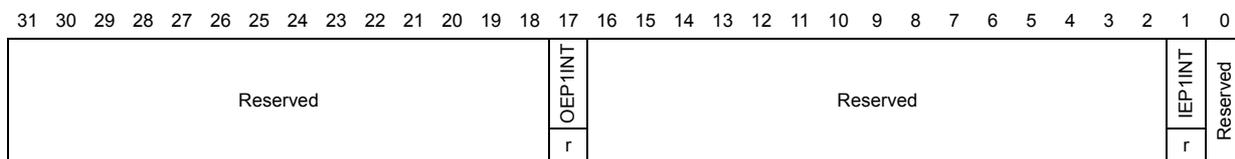
| 31 | 30 | 29 | 28 | 27 | 26 | 25 | 24 | 23 | 22 | 21 | 20 | 19 | 18 | 17 | 16 | 15 | 14 | 13 | 12 | 11 | 10 | 9 | 8 | 7 | 6 | 5 | 4 | 3 | 2 | 1 | 0 |
| Reserved | OEP1INT | Reserved | IEP1INT | Reserved | |||||||||||||||||||||||||||
| r | r | ||||||||||||||||||||||||||||||
Bits 31:18 Reserved, must be kept at reset value.
Bit 17 OEP1INT : OUT endpoint 1 interrupt bit
Bits 16:2 Reserved, must be kept at reset value.
Bit 1 IEP1INT : IN endpoint 1 interrupt bit
Bit 0 Reserved, must be kept at reset value.
OTG_HS device each endpoint interrupt register mask (OTG_HS_DEACHINTMSK)
Address offset: 0x083C
Reset value: 0x0000 0000
There is one interrupt bit for endpoint 1 IN and one interrupt bit for endpoint 1 OUT.
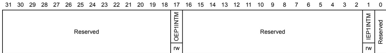
| 31 | 30 | 29 | 28 | 27 | 26 | 25 | 24 | 23 | 22 | 21 | 20 | 19 | 18 | 17 | 16 | 15 | 14 | 13 | 12 | 11 | 10 | 9 | 8 | 7 | 6 | 5 | 4 | 3 | 2 | 1 | 0 |
| Reserved | OEP1INTM rw | Reserved | IEP1INTM rw | Reserved | |||||||||||||||||||||||||||
Bits 31:18 Reserved, must be kept at reset value.
Bit 17 OEP1INTM : OUT Endpoint 1 interrupt mask bit
Bits 16:2 Reserved, must be kept at reset value.
Bit 1 IEP1INTM : IN Endpoint 1 interrupt mask bit
Bit 0 Reserved, must be kept at reset value.
OTG_HS device each in endpoint-1 interrupt register (OTG_HS_DIEPEACHMSK1)
Address offset: 0x844
Reset value: 0x0000 0000
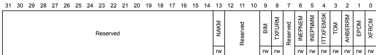
| 31 | 30 | 29 | 28 | 27 | 26 | 25 | 24 | 23 | 22 | 21 | 20 | 19 | 18 | 17 | 16 | 15 | 14 | 13 | 12 | 11 | 10 | 9 | 8 | 7 | 6 | 5 | 4 | 3 | 2 | 1 | 0 |
| Reserved | NAKM rw | Reserved | BIM rw | TXFURM rw | Reserved | INEPNEM rw | INEPNMM rw | ITTXFEMSK rw | TOM rw | AHBERRM rw | EPDM rw | XFRCM rw | |||||||||||||||||||
Bits 31:14 Reserved, must be kept at reset value.
Bit 13 NAKM : NAK interrupt mask
- 0: Masked interrupt
- 1: unmasked interrupt
Bit 12:10 Reserved, must be kept at reset value.
Bit 9 BIM : BNA interrupt mask
- 0: Masked interrupt
- 1: Unmasked interrupt
Bit 8 TXFURM : FIFO underrun mask
- 0: Masked interrupt
- 1: Unmasked interrupt
Bit 7 Reserved, must be kept at reset value.
- Bit 6
INEPNEM
: IN endpoint NAK effective mask
0: Masked interrupt
1: Unmasked interrupt - Bit 5
INEPNMM
: IN token received with EP mismatch mask
0: Masked interrupt
1: Unmasked interrupt - Bit 4
ITTXFEMSK
: IN token received when TxFIFO empty mask
0: Masked interrupt
1: Unmasked interrupt - Bit 3
TOM
: Timeout condition mask (nonisochronous endpoints)
0: Masked interrupt
1: Unmasked interrupt - Bit 2
AHBERRM
: AHB error mask
0: Masked interrupt
1: Unmasked interrupt - Bit 1
EPDM
: Endpoint disabled interrupt mask
0: Masked interrupt
1: Unmasked interrupt - Bit 0
XFRCM
: Transfer completed interrupt mask
0: Masked interrupt
1: Unmasked interrupt
OTG_HS device each OUT endpoint-1 interrupt register (OTG_HS_DOEPEACHMSK1)
Address offset: 0x884
Reset value: 0x0000 0000
| 31 | 30 | 29 | 28 | 27 | 26 | 25 | 24 | 23 | 22 | 21 | 20 | 19 | 18 | 17 | 16 | 15 | 14 | 13 | 12 | 11 | 10 | 9 | 8 | 7 | 6 | 5 | 4 | 3 | 2 | 1 | 0 |
|---|---|---|---|---|---|---|---|---|---|---|---|---|---|---|---|---|---|---|---|---|---|---|---|---|---|---|---|---|---|---|---|
| Reserved | NYETM | NAKM | BERRM | Reserved | BIM | TXFURM | Reserved | INEPNEM | INEPNMM | ITTXFEMSK | TOM | AHBERRM | EPDM | XFRCM | |||||||||||||||||
| rw | rw | rw | rw | rw | rw | rw | rw | rw | rw | rw | rw | ||||||||||||||||||||
Bits 31:15 Reserved, must be kept at reset value.
Bit 14 NYETM : NYET interrupt mask
- 0: Masked interrupt
- 1: Unmasked interrupt
Bit 13 NAKM : NAK interrupt mask
- 0: Masked interrupt
- 1: Unmasked interrupt
Bit 12 BERRM : Bubble error interrupt mask
- 0: Masked interrupt
- 1: Unmasked interrupt
Bit 11:10 Reserved, must be kept at reset value.
Bit 9 BIM : BNA interrupt mask
- 0: Masked interrupt
- 1: Unmasked interrupt
Bit 8 OPEM : OUT packet error mask
- 0: Masked interrupt
- 1: Unmasked interrupt
Bits 7:3 Reserved, must be kept at reset value.
Bit 2 AHBERRM : AHB error mask
- 0: Masked interrupt
- 1: Unmasked interrupt
Bit 1 EPDM : Endpoint disabled interrupt mask
- 0: Masked interrupt
- 1: Unmasked interrupt
Bit 0 XFRCM : Transfer completed interrupt mask
- 0: Masked interrupt
- 1: Unmasked interrupt
OTG device endpoint-x control register (OTG_HS_DIEPCTLx) (x = 0..5, where x = Endpoint_number)
Address offset: 0x900 + 0x20 * x
Reset value: 0x0000 0000
The application uses this register to control the behavior of each logical endpoint other than endpoint 0.
| 31 | 30 | 29 | 28 | 27 | 26 | 25 | 24 | 23 | 22 | 21 | 20 | 19 | 18 | 17 | 16 | 15 | 14 | 13 | 12 | 11 | 10 | 9 | 8 | 7 | 6 | 5 | 4 | 3 | 2 | 1 | 0 |
|---|---|---|---|---|---|---|---|---|---|---|---|---|---|---|---|---|---|---|---|---|---|---|---|---|---|---|---|---|---|---|---|
| EPENA | EPDIS | SODDFRM | SDPID/SEVNFRM | SNAK | CNAK | TXFNUM | Stall | Reserved | EPTYP | NAKSTS | EONUM/DPID | USBEP | Reserved | MPSIZ | |||||||||||||||||
| rs | rs | w | w | w | w | rw | rw | rw | rw | rw/rs | rw | rw | r | r | rw | rw | rw | rw | rw | rw | rw | rw | rw | rw | rw | rw | |||||
The application sets this bit to start transmitting data on an endpoint.
The core clears this bit before setting any of the following interrupts on this endpoint:
- – SETUP phase done
- – Endpoint disabled
- – Transfer completed
The application sets this bit to stop transmitting/receiving data on an endpoint, even before the transfer for that endpoint is complete. The application must wait for the Endpoint disabled interrupt before treating the endpoint as disabled. The core clears this bit before setting the Endpoint disabled interrupt. The application must set this bit only if Endpoint enable is already set for this endpoint.
Bit 29 SODDFRM: Set odd frameApplies to isochronous IN and OUT endpoints only.
Writing to this field sets the Even/Odd frame (EONUM) field to odd frame.
Bit 28 SD0PID: Set DATA0 PIDApplies to interrupt/bulk IN endpoints only.
Writing to this field sets the endpoint data PID (DPID) field in this register to DATA0.
SEVNFRM: Set even frameApplies to isochronous IN endpoints only.
Writing to this field sets the Even/Odd frame (EONUM) field to even frame.
Bit 27 SNAK: Set NAKA write to this bit sets the NAK bit for the endpoint.
Using this bit, the application can control the transmission of NAK handshakes on an endpoint. The core can also set this bit for OUT endpoints on a Transfer completed interrupt, or after a SETUP is received on the endpoint.
Bit 26 CNAK: Clear NAKA write to this bit clears the NAK bit for the endpoint.
Bits 25:22 TXFNUM: TxFIFO numberThese bits specify the FIFO number associated with this endpoint. Each active IN endpoint must be programmed to a separate FIFO number.
This field is valid only for IN endpoints.
Bit 21 STALL: STALL handshakeApplies to noncontrol, nonisochronous IN endpoints only (access type is rw).
The application sets this bit to stall all tokens from the USB host to this endpoint. If a NAK bit, Global IN NAK, or Global OUT NAK is set along with this bit, the STALL bit takes priority. Only the application can clear this bit, never the core.
Applies to control endpoints only (access type is rs).
The application can only set this bit, and the core clears it, when a SETUP token is received for this endpoint. If a NAK bit, Global IN NAK, or Global OUT NAK is set along with this bit, the STALL bit takes priority. Irrespective of this bit's setting, the core always responds to SETUP data packets with an ACK handshake.
Bit 20 Reserved, must be kept at reset value.Bits 19:18 EPType : Endpoint type
This is the transfer type supported by this logical endpoint.
00: Control
01: Isochronous
10: Bulk
11: Interrupt
Bit 17 NAKSTS : NAK status
It indicates the following:
0: The core is transmitting nonNAK handshakes based on the FIFO status.
1: The core is transmitting NAK handshakes on this endpoint.
When either the application or the core sets this bit:
For nonisochronous IN endpoints: The core stops transmitting any data on an IN endpoint, even if there are data available in the TxFIFO.
For isochronous IN endpoints: The core sends out a zero-length data packet, even if there are data available in the TxFIFO.
Irrespective of this bit's setting, the core always responds to SETUP data packets with an ACK handshake.
Bit 16 EONUM : Even/odd frame
Applies to isochronous IN endpoints only.
Indicates the frame number in which the core transmits/receives isochronous data for this endpoint. The application must program the even/odd frame number in which it intends to transmit/receive isochronous data for this endpoint using the SEVNFRM and SODDFRM fields in this register.
0: Even frame
1: Odd frame
DPID : Endpoint data PID
Applies to interrupt/bulk IN endpoints only.
Contains the PID of the packet to be received or transmitted on this endpoint. The application must program the PID of the first packet to be received or transmitted on this endpoint, after the endpoint is activated. The application uses the SD0PID register field to program either DATA0 or DATA1 PID.
0: DATA0
1: DATA1
Bit 15 USBAEP : USB active endpoint
Indicates whether this endpoint is active in the current configuration and interface. The core clears this bit for all endpoints (other than EP 0) after detecting a USB reset. After receiving the SetConfiguration and SetInterface commands, the application must program endpoint registers accordingly and set this bit.
Bits 14:11 Reserved, must be kept at reset value.
Bits 10:0 MPSIZ : Maximum packet size
The application must program this field with the maximum packet size for the current logical endpoint. This value is in bytes.
OTG_HS device control OUT endpoint 0 control register
(OTG_HS_DOEPCTL0)
Address offset: 0xB00
Reset value: 0x0000 8000
This section describes the device control OUT endpoint 0 control register. Nonzero control endpoints use registers for endpoints 1–15.
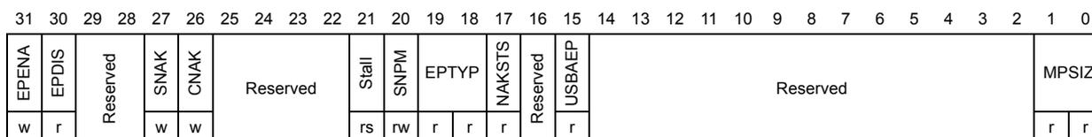
| 31 | 30 | 29 | 28 | 27 | 26 | 25 | 24 | 23 | 22 | 21 | 20 | 19 | 18 | 17 | 16 | 15 | 14 | 13 | 12 | 11 | 10 | 9 | 8 | 7 | 6 | 5 | 4 | 3 | 2 | 1 | 0 |
|---|---|---|---|---|---|---|---|---|---|---|---|---|---|---|---|---|---|---|---|---|---|---|---|---|---|---|---|---|---|---|---|
| EPENA | EPDIS | Reserved | SNAK | CNAK | Reserved | Stall | SNPM | EPTYP | NAKSTS | Reserved | USBAEP | Reserved | MPSIZ | ||||||||||||||||||
| w | r | w | w | rs | rw | r | r | r | r | r | r | r | |||||||||||||||||||
Bit 31 EPENA : Endpoint enable
The application sets this bit to start transmitting data on endpoint 0.
The core clears this bit before setting any of the following interrupts on this endpoint:
- – SETUP phase done
- – Endpoint disabled
- – Transfer completed
Bit 30 EPDIS : Endpoint disable
The application cannot disable control OUT endpoint 0.
Bits 29:28 Reserved, must be kept at reset value.
Bit 27 SNAK : Set NAK
A write to this bit sets the NAK bit for the endpoint.
Using this bit, the application can control the transmission of NAK handshakes on an endpoint. The core can also set this bit on a Transfer completed interrupt, or after a SETUP is received on the endpoint.
Bit 26 CNAK : Clear NAK
A write to this bit clears the NAK bit for the endpoint.
Bits 25:22 Reserved, must be kept at reset value.
Bit 21 STALL : STALL handshake
The application can only set this bit, and the core clears it, when a SETUP token is received for this endpoint. If a NAK bit or Global OUT NAK is set along with this bit, the STALL bit takes priority. Irrespective of this bit's setting, the core always responds to SETUP data packets with an ACK handshake.
Bit 20 SNPM : Snoop mode
This bit configures the endpoint to Snoop mode. In Snoop mode, the core does not check the correctness of OUT packets before transferring them to application memory.
Bits 19:18 EPTYP : Endpoint type
Hardcoded to 2'b00 for control.
Bit 17 NAKSTS : NAK status
Indicates the following:
- 0: The core is transmitting nonNAK handshakes based on the FIFO status.
- 1: The core is transmitting NAK handshakes on this endpoint.
When either the application or the core sets this bit, the core stops receiving data, even if there is space in the RxFIFO to accommodate the incoming packet. Irrespective of this bit's setting, the core always responds to SETUP data packets with an ACK handshake.
Bit 16 Reserved, must be kept at reset value.
Bit 15 USBAEP : USB active endpoint
This bit is always set to 1, indicating that a control endpoint 0 is always active in all configurations and interfaces.
Bits 14:2 Reserved, must be kept at reset value.
Bits 1:0 MPSIZ : Maximum packet size
The maximum packet size for control OUT endpoint 0 is the same as what is programmed in control IN endpoint 0.
- 00: 64 bytes
- 01: 32 bytes
- 10: 16 bytes
- 11: 8 bytes
OTG_HS device endpoint-x control register (OTG_HS_DOEPCTLx) (x = 1..5, where x = Endpoint_number)
Address offset for OUT endpoints: 0xB00 + 0x20 * x
Reset value: 0x0000 0000
The application uses this register to control the behavior of each logical endpoint other than endpoint 0.
| 31 | 30 | 29 | 28 | 27 | 26 | 25 | 24 | 23 | 22 | 21 | 20 | 19 | 18 | 17 | 16 | 15 | 14 | 13 | 12 | 11 | 10 | 9 | 8 | 7 | 6 | 5 | 4 | 3 | 2 | 1 | 0 | |
|---|---|---|---|---|---|---|---|---|---|---|---|---|---|---|---|---|---|---|---|---|---|---|---|---|---|---|---|---|---|---|---|---|
| EPENA | EPDIS | SODDFRM | SD0PID/SEVNFRM | SNAK | CNAK | Reserved | Stall | SNPM | EPTYP | NAKSTS | EONUM/DPID | USBAEP | Reserved | MPSIZ | ||||||||||||||||||
| rs | rs | w | w | w | w | rw | rw | rw | r | r | rw | rw | rw | rw | rw | rw | rw | rw | rw | rw | rw | rw | ||||||||||
Applies to IN and OUT endpoints.
The application sets this bit to start transmitting data on an endpoint.
The core clears this bit before setting any of the following interrupts on this endpoint:
- – SETUP phase done
- – Endpoint disabled
- – Transfer completed
The application sets this bit to stop transmitting/receiving data on an endpoint, even before the transfer for that endpoint is complete. The application must wait for the Endpoint disabled interrupt before treating the endpoint as disabled. The core clears this bit before setting the Endpoint disabled interrupt. The application must set this bit only if Endpoint enable is already set for this endpoint.
Bit 29 SODDFRM: Set odd frameApplies to isochronous OUT endpoints only.
Writing to this field sets the Even/Odd frame (EONUM) field to odd frame.
Bit 28 SD0PID: Set DATA0 PIDApplies to interrupt/bulk OUT endpoints only.
Writing to this field sets the endpoint data PID (DPID) field in this register to DATA0.
SEVNFRM: Set even frameApplies to isochronous OUT endpoints only.
Writing to this field sets the Even/Odd frame (EONUM) field to even frame.
Bit 27 SNAK: Set NAKA write to this bit sets the NAK bit for the endpoint.
Using this bit, the application can control the transmission of NAK handshakes on an endpoint. The core can also set this bit for OUT endpoints on a Transfer Completed interrupt, or after a SETUP is received on the endpoint.
Bit 26 CNAK: Clear NAKA write to this bit clears the NAK bit for the endpoint.
Bits 25:22 Reserved, must be kept at reset value.
Bit 21 STALL: STALL handshakeApplies to noncontrol, nonisochronous OUT endpoints only (access type is rw).
The application sets this bit to stall all tokens from the USB host to this endpoint. If a NAK bit, Global IN NAK, or Global OUT NAK is set along with this bit, the STALL bit takes priority. Only the application can clear this bit, never the core.
Bit 20 SNPM: Snoop modeThis bit configures the endpoint to Snoop mode. In Snoop mode, the core does not check the correctness of OUT packets before transferring them to application memory.
Bits 19:18 EPTYP: Endpoint typeThis is the transfer type supported by this logical endpoint.
00: Control
01: Isochronous
10: Bulk
11: Interrupt
Bit 17 NAKSTS: NAK statusIndicates the following:
- 0: The core is transmitting nonNAK handshakes based on the FIFO status.
- 1: The core is transmitting NAK handshakes on this endpoint.
When either the application or the core sets this bit:
The core stops receiving any data on an OUT endpoint, even if there is space in the RxFIFO to accommodate the incoming packet.
Irrespective of this bit's setting, the core always responds to SETUP data packets with an ACK handshake.
Bit 16 EONUM: Even/odd frameApplies to isochronous IN and OUT endpoints only.
Indicates the frame number in which the core transmits/receives isochronous data for this endpoint. The application must program the even/odd frame number in which it intends to transmit/receive isochronous data for this endpoint using the SEVNFRM and SODDFRM fields in this register.
- 0: Even frame
- 1: Odd frame
Applies to interrupt/bulk OUT endpoints only.
Contains the PID of the packet to be received or transmitted on this endpoint. The application must program the PID of the first packet to be received or transmitted on this endpoint, after the endpoint is activated. The application uses the SD0PID register field to program either DATA0 or DATA1 PID.
- 0: DATA0
- 1: DATA1
Indicates whether this endpoint is active in the current configuration and interface. The core clears this bit for all endpoints (other than EP 0) after detecting a USB reset. After receiving the SetConfiguration and SetInterface commands, the application must program endpoint registers accordingly and set this bit.
Bits 14:11 Reserved, must be kept at reset value.
Bits 10:0 MPSIZ: Maximum packet sizeThe application must program this field with the maximum packet size for the current logical endpoint. This value is in bytes.
OTG_HS device endpoint-x interrupt register (OTG_HS_DIEPINTx) (x = 0..5, where x = Endpoint_number)
Address offset: 0x908 + 0x20 * x
Reset value: 0x0000 0080
This register indicates the status of an endpoint with respect to USB- and AHB-related events. It is shown in Figure 414 . The application must read this register when the IN endpoints interrupt bit of the Core interrupt register (IEPINT in OTG_HS_GINTSTS) is set. Before the application can read this register, it must first read the device all endpoints interrupt (OTG_HS_DAINT) register to get the exact endpoint number for the device endpoint-x interrupt register. The application must clear the appropriate bit in this register to clear the corresponding bits in the OTG_HS_DAINT and OTG_HS_GINTSTS registers.
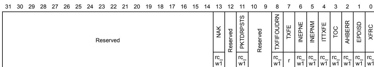
| 31 | 30 | 29 | 28 | 27 | 26 | 25 | 24 | 23 | 22 | 21 | 20 | 19 | 18 | 17 | 16 | 15 | 14 | 13 | 12 | 11 | 10 | 9 | 8 | 7 | 6 | 5 | 4 | 3 | 2 | 1 | 0 |
|---|---|---|---|---|---|---|---|---|---|---|---|---|---|---|---|---|---|---|---|---|---|---|---|---|---|---|---|---|---|---|---|
| Reserved | NAK | Reserved | PKTDRPSTS | Reserved | TXFIFOUDRN | TXFE | INEPNE | INEPNM | ITTXFE | TOC | AHBERR | EPDISD | XFRC | ||||||||||||||||||
| rc_w1 | rc_w1 | rc_w1 | r | rc_w1 | rc_w1 | rc_w1 | rc_w1 | rc_w1 | rc_w1 | ||||||||||||||||||||||
Bits 31:14 Reserved, must be kept at reset value.
Bit 13 NAK : NAK interrupt
The core generates this interrupt when a NAK is transmitted or received by the device. In case of isochronous IN endpoints the interrupt gets generated when a zero length packet is transmitted due to unavailability of data in the Tx FIFO.
Bit 12 Reserved, must be kept at reset value.
Bit 11 PKTDRPSTS : Packet dropped status
This bit indicates to the application that an ISOC OUT packet has been dropped. This bit does not have an associated mask bit and does not generate an interrupt.
Bits 10:9 Reserved, must be kept at reset value.
Bit 8 TXFIFOUDRN : Transmit Fifo Underrun (TxfifoUndrn) The core generates this interrupt when it detects a transmit FIFO underrun condition for this endpoint.
Dependency : This interrupt is valid only when Thresholding is enabled
Bit 7 TXFE : Transmit FIFO empty
This interrupt is asserted when the TxFIFO for this endpoint is either half or completely empty. The half or completely empty status is determined by the TxFIFO empty level bit in the Core AHB configuration register (TXFELVL bit in OTG_HS_GAHBCFG).
Bit 6 INEPNE : IN endpoint NAK effective
This bit can be cleared when the application clears the IN endpoint NAK by writing to the CNAK bit in OTG_HS_DIEPCTLx.
This interrupt indicates that the core has sampled the NAK bit set (either by the application or by the core). The interrupt indicates that the IN endpoint NAK bit set by the application has taken effect in the core.
This interrupt does not guarantee that a NAK handshake is sent on the USB. A STALL bit takes priority over a NAK bit.
Bit 5 INEPNM: IN token received with EP mismatchIndicates that the data in the top of the non-periodic TxFIFO belongs to an endpoint other than the one for which the IN token was received. This interrupt is asserted on the endpoint for which the IN token was received.
Bit 4 ITTXFE: IN token received when TxFIFO is emptyApplies to nonperiodic IN endpoints only.
Indicates that an IN token was received when the associated TxFIFO (periodic/nonperiodic) was empty. This interrupt is asserted on the endpoint for which the IN token was received.
Bit 3 TOC: Timeout conditionApplies only to Control IN endpoints.
Indicates that the core has detected a timeout condition on the USB for the last IN token on this endpoint.
Bit 2 AHBERR: AHB errorThis is generated only in internal DMA mode when there is an AHB error during an AHB read/write. The application can read the corresponding endpoint DMA address register to get the error address.
Bit 1 EPDISD: Endpoint disabled interruptThis bit indicates that the endpoint is disabled per the application's request.
Bit 0 XFRC: Transfer completed interruptThis field indicates that the programmed transfer is complete on the AHB as well as on the USB, for this endpoint.
OTG_HS device endpoint-x interrupt register (OTG_HS_DOEPINTx) (x = 0..5, where x = Endpoint_number)
Address offset: 0xB08 + 0x20 * x
Reset value: 0x0000 0080
This register indicates the status of an endpoint with respect to USB- and AHB-related events. It is shown in Figure 414 . The application must read this register when the OUT Endpoints Interrupt bit of the Core interrupt register (OEPINT bit in OTG_HS_GINTSTS) is set. Before the application can read this register, it must first read the device all endpoints interrupt (OTG_HS_DAINT) register to get the exact endpoint number for the device Endpoint-x interrupt register. The application must clear the appropriate bit in this register to clear the corresponding bits in the OTG_HS_DAINT and OTG_HS_GINTSTS registers.
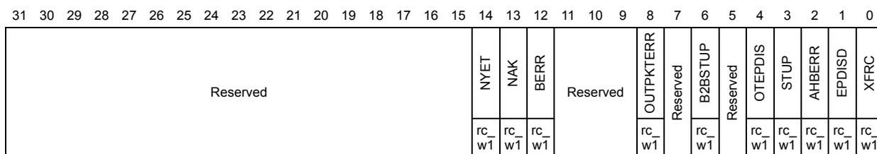
| 31 | 30 | 29 | 28 | 27 | 26 | 25 | 24 | 23 | 22 | 21 | 20 | 19 | 18 | 17 | 16 | 15 | 14 | 13 | 12 | 11 | 10 | 9 | 8 | 7 | 6 | 5 | 4 | 3 | 2 | 1 | 0 |
|---|---|---|---|---|---|---|---|---|---|---|---|---|---|---|---|---|---|---|---|---|---|---|---|---|---|---|---|---|---|---|---|
| Reserved | NYET | NAK | BERR | Reserved | OUTPKTERR | Reserved | B2BSTUP | Reserved | OTEPDIS | STUP | AHBERR | EPDISD | XRC | ||||||||||||||||||
| rc_w1 | rc_w1 | rc_w1 | rc_w1 | rc_w1 | rc_w1 | rc_w1 | rc_w1 | rc_w1 | rc_w1 | ||||||||||||||||||||||
Bits 31:15 Reserved, must be kept at reset value.
Bit 14 NYET : NYET interrupt
The core generates this interrupt when a NYET response is transmitted for a nonisochronous OUT endpoint.
Bit 13 NAK : NAK input
The core generates this interrupt when a NAK is transmitted or received by the device. In case of isochronous IN endpoints the interrupt gets generated when a zero length packet is transmitted due to unavailability of data in the Tx FIFO.
Bit 12 BERR : Babble error interrupt
The core generates this interrupt when babble is received for the endpoint.
Bits 11:9 Reserved, must be kept at reset value.
Bit 8 OUTPKTERR : OUT packet error
This interrupt is asserted when the core detects an overflow or a CRC error for an OUT packet. This interrupt is valid only when thresholding is enabled.
Bit 7 Reserved, must be kept at reset value.
Bit 6 B2BSTUP : Back-to-back SETUP packets received
Applies to Control OUT endpoint only.
This bit indicates that the core has received more than three back-to-back SETUP packets for this particular endpoint.
Bit 5 Reserved, must be kept at reset value.
Bit 4 OTEPDIS : OUT token received when endpoint disabled
Applies only to control OUT endpoint.
Indicates that an OUT token was received when the endpoint was not yet enabled. This interrupt is asserted on the endpoint for which the OUT token was received.
Bit 3 STUP : SETUP phase doneApplies to control OUT endpoints only.
Indicates that the SETUP phase for the control endpoint is complete and no more back-to-back SETUP packets were received for the current control transfer. On this interrupt, the application can decode the received SETUP data packet.
Bit 2 AHBERR : AHB errorThis is generated only in internal DMA mode when there is an AHB error during an AHB read/write. The application can read the corresponding endpoint DMA address register to get the error address.
Bit 1 EPDISD : Endpoint disabled interruptThis bit indicates that the endpoint is disabled per the application's request.
Bit 0 XFR : Transfer completed interruptThis field indicates that the programmed transfer is complete on the AHB as well as on the USB, for this endpoint.
OTG_HS device IN endpoint 0 transfer size register (OTG_HS_DIEPTSIZ0)Address offset: 0x910
Reset value: 0x0000 0000
The application must modify this register before enabling endpoint 0. Once endpoint 0 is enabled using the endpoint enable bit in the device control endpoint 0 control registers (EPENA in OTG_HS_DIEPCTL0), the core modifies this register. The application can only read this register once the core has cleared the Endpoint enable bit.
Nonzero endpoints use the registers for endpoints 1–15.

| 31 | 30 | 29 | 28 | 27 | 26 | 25 | 24 | 23 | 22 | 21 | 20 | 19 | 18 | 17 | 16 | 15 | 14 | 13 | 12 | 11 | 10 | 9 | 8 | 7 | 6 | 5 | 4 | 3 | 2 | 1 | 0 |
| Reserved | PKTCNT | Reserved | XFRSIZ | ||||||||||||||||||||||||||||
| rw | rw | rw | rw | rw | rw | rw | rw | rw | |||||||||||||||||||||||
Bits 31:21 Reserved, must be kept at reset value.
Bits 20:19 PKTCNT : Packet countIndicates the total number of USB packets that constitute the Transfer Size amount of data for endpoint 0.
This field is decremented every time a packet (maximum size or short packet) is read from the TxFIFO.
Bits 18:7 Reserved, must be kept at reset value.
Bits 6:0 XFRSIZ : Transfer sizeIndicates the transfer size in bytes for endpoint 0. The core interrupts the application only after it has exhausted the transfer size amount of data. The transfer size can be set to the maximum packet size of the endpoint, to be interrupted at the end of each packet.
The core decrements this field every time a packet from the external memory is written to the TxFIFO.
OTG_HS device OUT endpoint 0 transfer size register (OTG_HS_DOEPTSIZ0)
Address offset: 0xB10
Reset value: 0x0000 0000
The application must modify this register before enabling endpoint 0. Once endpoint 0 is enabled using the Endpoint enable bit in the device control endpoint 0 control registers (EPENA bit in OTG_HS_DOEPCTL0), the core modifies this register. The application can only read this register once the core has cleared the Endpoint enable bit.
Nonzero endpoints use the registers for endpoints 1–15.
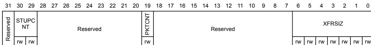
| 31 | 30 | 29 | 28 | 27 | 26 | 25 | 24 | 23 | 22 | 21 | 20 | 19 | 18 | 17 | 16 | 15 | 14 | 13 | 12 | 11 | 10 | 9 | 8 | 7 | 6 | 5 | 4 | 3 | 2 | 1 | 0 | |||||||
| Reserved | STUPCNT | Reserved | PKTCNT | Reserved | XFRSIZ | |||||||||||||||||||||||||||||||||
| rw | rw | rw | rw | rw | rw | rw | rw | rw | ||||||||||||||||||||||||||||||
Bit 31 Reserved, must be kept at reset value.
Bits 30:29 STUPCNT : SETUP packet count
This field specifies the number of back-to-back SETUP data packets the endpoint can receive.
01: 1 packet
10: 2 packets
11: 3 packets
Bits 28:20 Reserved, must be kept at reset value.
Bit 19 PKTCNT : Packet count
This field is decremented to zero after a packet is written into the RxFIFO.
Bits 18:7 Reserved, must be kept at reset value.
Bits 6:0 XFRSIZ : Transfer size
Indicates the transfer size in bytes for endpoint 0. The core interrupts the application only after it has exhausted the transfer size amount of data. The transfer size can be set to the maximum packet size of the endpoint, to be interrupted at the end of each packet.
The core decrements this field every time a packet is read from the RxFIFO and written to the external memory.
OTG_HS device endpoint-x transfer size register (OTG_HS_DIEPTSIZx)
(x = 1..5, where x = Endpoint_number)
Address offset: 0x910 + 0x20 * x
Reset value: 0x0000 0000
The application must modify this register before enabling the endpoint. Once the endpoint is enabled using the Endpoint enable bit in the device endpoint-x control registers (EPENA bit in OTG_HS_DIEPCTLx), the core modifies this register. The application can only read this register once the core has cleared the Endpoint enable bit.

| 31 | 30 | 29 | 28 | 27 | 26 | 25 | 24 | 23 | 22 | 21 | 20 | 19 | 18 | 17 | 16 | 15 | 14 | 13 | 12 | 11 | 10 | 9 | 8 | 7 | 6 | 5 | 4 | 3 | 2 | 1 | 0 |
| Reserved | MCNT | PKTCNT | XFRSIZ | ||||||||||||||||||||||||||||
| rw | rw | rw | rw | rw | rw | rw | rw | rw | rw | rw | rw | rw | rw | rw | rw | rw | rw | rw | rw | rw | rw | rw | rw | rw | rw | rw | rw | rw | rw | rw | rw |
Bit 31 Reserved, must be kept at reset value.
Bits 30:29 MCNT : Multi count
For periodic IN endpoints, this field indicates the number of packets that must be transmitted per frame on the USB. The core uses this field to calculate the data PID for isochronous IN endpoints.
01: 1 packet
10: 2 packets
11: 3 packets
Bit 28:19 PKTCNT : Packet count
Indicates the total number of USB packets that constitute the Transfer Size amount of data for this endpoint.
This field is decremented every time a packet (maximum size or short packet) is read from the TxFIFO.
Bits 18:0 XFRSIZ : Transfer size
This field contains the transfer size in bytes for the current endpoint. The core only interrupts the application after it has exhausted the transfer size amount of data. The transfer size can be set to the maximum packet size of the endpoint, to be interrupted at the end of each packet.
The core decrements this field every time a packet from the external memory is written to the TxFIFO.
OTG_HS device IN endpoint transmit FIFO status register (OTG_HS_DTXFSTx) (x = 0..5, where x = Endpoint_number)
Address offset for IN endpoints: \( 0x918 + 0x20 * x \)
This read-only register contains the free space information for the Device IN endpoint Tx FIFO.

| 31 | 30 | 29 | 28 | 27 | 26 | 25 | 24 | 23 | 22 | 21 | 20 | 19 | 18 | 17 | 16 | 15 | 14 | 13 | 12 | 11 | 10 | 9 | 8 | 7 | 6 | 5 | 4 | 3 | 2 | 1 | 0 |
| Reserved | INEPTFSAV | ||||||||||||||||||||||||||||||
| r | r | r | r | r | r | r | r | r | r | r | r | r | r | r | r | ||||||||||||||||
31:16 Reserved, must be kept at reset value.
15:0 INEPTFSAV : IN endpoint TxFIFO space avail ()
- Indicates the amount of free space available in the Endpoint TxFIFO.
- Values are in terms of 32-bit words:
- 0x0: Endpoint TxFIFO is full
- 0x1: 1 word available
- 0x2: 2 words available
- 0xn: n words available ( \( 0 < n < 512 \) )
- Others: Reserved
OTG_HS device endpoint-x transfer size register (OTG_HS_DOEPTSIZx) (x = 1..5, where x = Endpoint_number)
Address offset: \( 0xB10 + 0x20 * x \)
Reset value: 0x0000 0000
The application must modify this register before enabling the endpoint. Once the endpoint is enabled using Endpoint Enable bit of the device endpoint-x control registers (EPENA bit in OTG_HS_DOEPCTLx), the core modifies this register. The application can only read this register once the core has cleared the Endpoint enable bit.

| 31 | 30 | 29 | 28 | 27 | 26 | 25 | 24 | 23 | 22 | 21 | 20 | 19 | 18 | 17 | 16 | 15 | 14 | 13 | 12 | 11 | 10 | 9 | 8 | 7 | 6 | 5 | 4 | 3 | 2 | 1 | 0 |
| Reserved | RXDPID/ | TUPCNT | PKTCNT | XFRSIZ | |||||||||||||||||||||||||||
| r/w | r/w | rw | rw | rw | rw | rw | rw | rw | rw | rw | rw | rw | rw | rw | rw | rw | rw | rw | rw | rw | rw | rw | rw | rw | rw | rw | rw | rw | rw | rw | |
Bit 31 Reserved, must be kept at reset value.
Bits 30:29 RXDPID : Received data PID (access type is "r")
Applies to isochronous OUT endpoints only.
This is the data PID received in the last packet for this endpoint.
00: DATA0
01: DATA2
10: DATA1
11: MDATA
STUPCNT : SETUP packet count (access type is "rw")
Applies to control OUT Endpoints only.
This field specifies the number of back-to-back SETUP data packets the endpoint can receive.
01: 1 packet
10: 2 packets
11: 3 packets
Bit 28:19 PKTCNT : Packet count
Indicates the total number of USB packets that constitute the Transfer Size amount of data for this endpoint.
This field is decremented every time a packet (maximum size or short packet) is written to the RxFIFO.
Bits 18:0 XFRSIZ : Transfer size
This field contains the transfer size in bytes for the current endpoint. The core only interrupts the application after it has exhausted the transfer size amount of data. The transfer size can be set to the maximum packet size of the endpoint, to be interrupted at the end of each packet.
The core decrements this field every time a packet is read from the RxFIFO and written to the external memory.
OTG_HS device endpoint-x DMA address register (OTG_HS_DIEPDMAX / OTG_HS_DOEPDMAX) (x = 0..5, where x = Endpoint_number)
Address offset for IN endpoints: 0x914 + 0x20 * x
Reset value: 0xXXXX XXXX
Address offset for OUT endpoints: 0xB14 + 0x20 * x
Reset value: 0xXXXX XXXX
| 31 | 30 | 29 | 28 | 27 | 26 | 25 | 24 | 23 | 22 | 21 | 20 | 19 | 18 | 17 | 16 | 15 | 14 | 13 | 12 | 11 | 10 | 9 | 8 | 7 | 6 | 5 | 4 | 3 | 2 | 1 | 0 |
|---|---|---|---|---|---|---|---|---|---|---|---|---|---|---|---|---|---|---|---|---|---|---|---|---|---|---|---|---|---|---|---|
| DMAADDR | |||||||||||||||||||||||||||||||
| rw | rw | rw | rw | rw | rw | rw | rw | rw | rw | rw | rw | rw | rw | rw | rw | rw | rw | rw | rw | rw | rw | rw | rw | rw | rw | rw | rw | rw | rw | rw | rw |
Bits 31:0 DMAADDR : DMA address
This bit holds the start address of the external memory for storing or fetching endpoint data.
Note: For control endpoints, this field stores control OUT data packets as well as SETUP transaction data packets. When more than three SETUP packets are received back-to-back, the SETUP data packet in the memory is overwritten. This register is incremented on every AHB transaction. The application can give only a word-aligned address.
35.12.5 OTG_HS power and clock gating control register (OTG_HS_PCGCTL)
Address offset: 0xE00
Reset value: 0x0000 0000
This register is available in host and peripheral modes.
| 31 | 30 | 29 | 28 | 27 | 26 | 25 | 24 | 23 | 22 | 21 | 20 | 19 | 18 | 17 | 16 | 15 | 14 | 13 | 12 | 11 | 10 | 9 | 8 | 7 | 6 | 5 | 4 | 3 | 2 | 1 | 0 |
| Reserved | PHYSUSP | Reserved | GATEHCLK | STPPCLK | |||||||||||||||||||||||||||
| rw | rw | rw | |||||||||||||||||||||||||||||
Bit 31:5 Reserved, must be kept at reset value.
Bit 4 PHYSUSP : PHY suspended
Indicates that the PHY has been suspended. This bit is updated once the PHY is suspended after the application has set the STPPCLK bit (bit 0).
Bits 3:2 Reserved, must be kept at reset value.
Bit 1 GATEHCLK : Gate HCLK
The application sets this bit to gate HCLK to modules other than the AHB Slave and Master and wake-up logic when the USB is suspended or the session is not valid. The application clears this bit when the USB is resumed or a new session starts.
Bit 0 STPPCLK : Stop PHY clock
The application sets this bit to stop the PHY clock when the USB is suspended, the session is not valid, or the device is disconnected. The application clears this bit when the USB is resumed or a new session starts.
35.12.6 OTG_HS register map
The table below gives the USB OTG register map and reset values.
Table 216. OTG_HS register map and reset values
| Offset | Register | 31 | 30 | 29 | 28 | 27 | 26 | 25 | 24 | 23 | 22 | 21 | 20 | 19 | 18 | 17 | 16 | 15 | 14 | 13 | 12 | 11 | 10 | 9 | 8 | 7 | 6 | 5 | 4 | 3 | 2 | 1 | 0 |
|---|---|---|---|---|---|---|---|---|---|---|---|---|---|---|---|---|---|---|---|---|---|---|---|---|---|---|---|---|---|---|---|---|---|
| 0x000 | OTG_HS_GO TGCTL | Reserved | BSVLD | ASVLD | DBCT | CIDSTS | Reserved | DHNPEN | HSHNPEN | HNPRQ | HNGSCS | Reserved | SRQ | SRQSCS | |||||||||||||||||||
| Reset value | 0 | 0 | 0 | 1 | 0 | 0 | 0 | 0 | 0 | 0 | |||||||||||||||||||||||
| 0x004 | OTG_HS_GO TGINT | Reserved | DBCDNE | ADTOCHG | HNGDET | Reserved | HNSSCHG | SRSSCHG | Reserved | SEDET | Res. | ||||||||||||||||||||||
| Reset value | 0 | 0 | 0 | 0 | 0 | 0 | |||||||||||||||||||||||||||
| 0x008 | OTG_HS_GA HBCFG | Reserved | PTXFELVL | TXFELVL | Reserved | GINT | |||||||||||||||||||||||||||
| Reset value | 0 | 0 | 0 | ||||||||||||||||||||||||||||||
Table 216. OTG_HS register map and reset values (continued)
| Offset | Register | 31 | 30 | 29 | 28 | 27 | 26 | 25 | 24 | 23 | 22 | 21 | 20 | 19 | 18 | 17 | 16 | 15 | 14 | 13 | 12 | 11 | 10 | 9 | 8 | 7 | 6 | 5 | 4 | 3 | 2 | 1 | 0 | ||
|---|---|---|---|---|---|---|---|---|---|---|---|---|---|---|---|---|---|---|---|---|---|---|---|---|---|---|---|---|---|---|---|---|---|---|---|
| 0x00C | OTG_HS_GUSBCFG | CTXPKT | FDMOD | FHMOD | Reserved | ULPIIPD | PTCI | PCCI | TSDPS | ULPIEVBUS1 | ULPIEVBUS2 | ULPICSM | ULPIAR | ULPIFSLS | Reserved | PHYLPCS | Reserved | TRDT | HNP CAP | SRPCAP | Reserved | PHYSEL | Reserved | TOTAL | |||||||||||
| Reset value | 0 | 0 | 0 | 0 | 0 | 0 | 0 | 0 | 0 | 0 | 0 | 0 | 0 | 0 | 0 | 1 | |||||||||||||||||||
| 0x010 | OTG_HS_GRSTCTL | AHBIDL | DMAREQ | Reserved | |||||||||||||||||||||||||||||||
| Reset value | 1 | 0 | |||||||||||||||||||||||||||||||||
| 0x014 | OTG_HS_GINTSTS | WKINT | SRQINT | DISINT | CIDSCHG | Reserved | PTXFE | HCINT | HPRTINT | Reserved | DATAFSUSP | IPXFR/INCOMPISOOUT | IISOXFR | OEPINT | IEPINT | Reserved | EOPF | ISOODRP | ENUMDNE | USBRST | USBUSUSP | ESUSP | Reserved | GONAKEFF | GINAKEFF | NPTXFE | RXFLVL | SOF | OTGINT | MMIS | CMOD | ||||
| Reset value | 0 | 0 | 0 | 0 | 1 | 0 | 0 | 0 | 0 | 0 | 0 | 0 | 0 | 0 | 0 | 0 | 0 | 0 | 0 | 0 | 1 | 0 | 0 | 0 | 0 | 0 | |||||||||
| 0x018 | OTG_HS_GINTMSK | WUIM | SRQIM | DISINT | CIDSCHGIM | Reserved | PTXFEM | HCIM | PRTIM | Reserved | FSUSPIM | IPXFRM/ISOOXFRM | IISOXFRM | OEPINT | IEPINT | Reserved | EOPFM | ISOODRPM | ENUMDNEM | USBRST | USBUSUSPM | ESUSPM | Reserved | GONAKEFFM | GINAKEFFM | NPTXFEM | RXFLVLM | SOFM | OTGINT | MMISM | Reserved | ||||
| Reset value | 0 | 0 | 0 | 0 | 0 | 0 | 0 | 0 | 0 | 0 | 0 | 0 | 0 | 0 | 0 | 0 | 0 | 0 | 0 | 0 | 0 | 0 | 0 | 0 | 0 | 0 | |||||||||
| 0x01C | OTG_HS_GRXSTSR (Host mode) | Reserved | PKTSTS | DPID | BCNT | CHNUM | |||||||||||||||||||||||||||||
| Reset value | 0 | 0 | |||||||||||||||||||||||||||||||||
| OTG_HS_GRXSTSR (peripheral mode) | Reserved | FRMNUM | PKTSTS | DPID | BCNT | EPNUM | |||||||||||||||||||||||||||||
| Reset value | 0 | 0 | 0 | ||||||||||||||||||||||||||||||||
| 0x020 | OTG_HS_GRXSTSP (Host mode) | Reserved | PKTSTS | DPID | BCNT | CHNUM | |||||||||||||||||||||||||||||
| Reset value | 0 | 0 | |||||||||||||||||||||||||||||||||
| OTG_HS_GRXSTSP (peripheral mode) | Reserved | FRMNUM | PKTSTS | DPID | BCNT | EPNUM | |||||||||||||||||||||||||||||
| Reset value | 0 | 0 | 0 | ||||||||||||||||||||||||||||||||
| 0x024 | OTG_HS_GRXFSIZ | Reserved | RXFD | ||||||||||||||||||||||||||||||||
| Reset value | 0 | ||||||||||||||||||||||||||||||||||
| Offset | Register | 31 | 30 | 29 | 28 | 27 | 26 | 25 | 24 | 23 | 22 | 21 | 20 | 19 | 18 | 17 | 16 | 15 | 14 | 13 | 12 | 11 | 10 | 9 | 8 | 7 | 6 | 5 | 4 | 3 | 2 | 1 | 0 |
|---|---|---|---|---|---|---|---|---|---|---|---|---|---|---|---|---|---|---|---|---|---|---|---|---|---|---|---|---|---|---|---|---|---|
| 0x028 | OTG_HS_GNPTXFSIZ (Host mode) | NPTXFD | NPTXFSA | ||||||||||||||||||||||||||||||
| Reset value | 0 | 0 | 0 | 0 | 0 | 0 | 0 | 0 | 0 | 0 | 0 | 0 | 0 | 0 | 0 | 0 | 0 | 0 | 0 | 0 | 0 | 0 | 1 | 0 | 0 | 0 | 0 | 0 | 0 | 0 | 0 | 0 | |
| OTG_HS_GNPTXFSIZ (peripheral mode) | TX0FD | TX0FSA | |||||||||||||||||||||||||||||||
| Reset value | 0 | 0 | 0 | 0 | 0 | 0 | 0 | 0 | 0 | 0 | 0 | 0 | 0 | 0 | 0 | 0 | 0 | 0 | 0 | 0 | 0 | 0 | 1 | 0 | 0 | 0 | 0 | 0 | 0 | 0 | 0 | 0 | |
| 0x02C | OTG_HS_GNPTXSTS | Res. | NPTXQTOP | NPTQXSAV | NPTXFSAV | ||||||||||||||||||||||||||||
| Reset value | 0 | 0 | 0 | 0 | 0 | 0 | 0 | 0 | 0 | 0 | 1 | 0 | 0 | 0 | 0 | 0 | 0 | 0 | 1 | 0 | 0 | 0 | 0 | 0 | 0 | 0 | 0 | 0 | 0 | 0 | 0 | ||
| 0x030 | OTG_HS_GI2CCTL | BSYDNE | RW | Reserved | I2CDATSE0 | I2CDEVADR | Reserved | ACK | I2CEN | ADDR | REGADDR | RWDATA | |||||||||||||||||||||
| 0x038 | OTG_HS_GCCFG | Reserved | NOVBUSSENS | SOFOUTEN | VBUSSEN | VBUSASEN | I2CPADEN | .PWRDWN | Reserved | ||||||||||||||||||||||||
| Reset value | 0 | 0 | 0 | 0 | 0 | 0 | |||||||||||||||||||||||||||
| 0x03C | OTG_HS_CID | PRODUCT_ID | |||||||||||||||||||||||||||||||
| Reset value | 0 | 0 | 0 | 0 | 0 | 0 | 0 | 0 | 0 | 0 | 0 | 0 | 0 | 0 | 0 | 0 | 0 | 0 | 0 | 1 | 0 | 0 | 0 | 1 | 0 | 0 | 0 | 0 | 0 | 0 | 0 | 0 | |
| 0x100 | OTG_HS_HPTXFSIZ | PTXFD | PTXSA | ||||||||||||||||||||||||||||||
| Reset value | 0 | 0 | 0 | 0 | 0 | 0 | 1 | 0 | 0 | 0 | 0 | 0 | 0 | 0 | 0 | 0 | 0 | 0 | 0 | 1 | 0 | 0 | 0 | 0 | 0 | 0 | 0 | 0 | 0 | 0 | 0 | 0 | |
| 0x104 | OTG_HS_DIEPTXF1 | INEPTXFD | INEPTXSA | ||||||||||||||||||||||||||||||
| Reset value | 0 | 0 | 0 | 0 | 0 | 0 | 1 | 0 | 0 | 0 | 0 | 0 | 0 | 0 | 0 | 0 | 0 | 0 | 0 | 1 | 0 | 0 | 0 | 0 | 0 | 0 | 0 | 0 | 0 | 0 | 0 | 0 | |
| 0x108 | OTG_HS_DIEPTXF2 | INEPTXFD | INEPTXSA | ||||||||||||||||||||||||||||||
| Reset value | 0 | 0 | 0 | 0 | 0 | 0 | 1 | 0 | 0 | 0 | 0 | 0 | 0 | 0 | 0 | 0 | 0 | 0 | 0 | 1 | 0 | 0 | 0 | 0 | 0 | 0 | 0 | 0 | 0 | 0 | 0 | 0 | |
| 0x10C | OTG_HS_DIEPTXF3 | INEPTXFD | INEPTXSA | ||||||||||||||||||||||||||||||
| Reset value | 0 | 0 | 0 | 0 | 0 | 0 | 1 | 0 | 0 | 0 | 0 | 0 | 0 | 0 | 0 | 0 | 0 | 0 | 0 | 1 | 0 | 0 | 0 | 0 | 0 | 0 | 0 | 0 | 0 | 0 | 0 | 0 | |
| 0x110 | OTG_HS_DIEPTXF4 | INEPTXFD | INEPTXSA | ||||||||||||||||||||||||||||||
| Reset value | 0 | 0 | 0 | 0 | 0 | 0 | 1 | 0 | 0 | 0 | 0 | 0 | 0 | 0 | 0 | 0 | 0 | 0 | 0 | 1 | 0 | 0 | 0 | 0 | 0 | 0 | 0 | 0 | 0 | 0 | 0 | 0 | |
| 0x400 | OTG_HS_HCFG | Reserved | FSLSS | FSLSPCS | |||||||||||||||||||||||||||||
| Reset value | 0 | 0 | 0 | ||||||||||||||||||||||||||||||
| 0x404 | OTG_HS_HFIR | Reserved | FRIVL | ||||||||||||||||||||||||||||||
| Reset value | 1 | 1 | 1 | 0 | 1 | 0 | 1 | 0 | 0 | 1 | 1 | 0 | 0 | 0 | 0 | 0 | 0 | ||||||||||||||||
| 0x408 | OTG_HS_HFNUM | FTREM | FRNUM | ||||||||||||||||||||||||||||||
| Reset value | 0 | 0 | 0 | 0 | 0 | 0 | 0 | 0 | 0 | 0 | 0 | 0 | 0 | 0 | 0 | 0 | 0 | 1 | 1 | 1 | 1 | 1 | 1 | 1 | 1 | 1 | 1 | 1 | 1 | 1 | 1 | 1 | |
| 0x410 | OTG_HS_HPTXSTS | PTXQTOP | PTXQSAV | PTXFSAVL | |||||||||||||||||||||||||||||
| Reset value | 0 | 0 | 0 | 0 | 0 | 0 | 0 | 0 | Y | Y | Y | Y | Y | Y | Y | Y | Y | Y | Y | Y | Y | Y | Y | Y | Y | Y | Y | Y | Y | Y | Y | Y | |
Table 216. OTG_HS register map and reset values (continued)
| Offset | Register | 31 | 30 | 29 | 28 | 27 | 26 | 25 | 24 | 23 | 22 | 21 | 20 | 19 | 18 | 17 | 16 | 15 | 14 | 13 | 12 | 11 | 10 | 9 | 8 | 7 | 6 | 5 | 4 | 3 | 2 | 1 | 0 |
|---|---|---|---|---|---|---|---|---|---|---|---|---|---|---|---|---|---|---|---|---|---|---|---|---|---|---|---|---|---|---|---|---|---|
| 0x414 | OTG_HS_HAINT | Reserved | HAINT | ||||||||||||||||||||||||||||||
| Reset value | 0 | 0 | 0 | 0 | 0 | 0 | 0 | 0 | 0 | 0 | 0 | 0 | 0 | 0 | 0 | 0 | 0 | 0 | 0 | 0 | 0 | 0 | 0 | 0 | 0 | 0 | 0 | 0 | 0 | 0 | 0 | 0 | |
| 0x418 | OTG_HS_HAINTMSK | Reserved | HAINTM | ||||||||||||||||||||||||||||||
| Reset value | 0 | 0 | 0 | 0 | 0 | 0 | 0 | 0 | 0 | 0 | 0 | 0 | 0 | 0 | 0 | 0 | 0 | 0 | 0 | 0 | 0 | 0 | 0 | 0 | 0 | 0 | 0 | 0 | 0 | 0 | 0 | 0 | |
| 0x440 | OTG_HS_HPRT | Reserved | PSPD | PTCTL | PPWR | PLSTS | Reserved | PRST | PSUSP | PRES | POCCHNG | POCA | PENCHNG | PENA | PCDET | PCSTS | |||||||||||||||||
| Reset value | 0 | 0 | 0 | 0 | 0 | 0 | 0 | 0 | 0 | 0 | 0 | 0 | 0 | 0 | 0 | 0 | 0 | 0 | |||||||||||||||
| 0x500 | OTG_HS_HCCHAR0 | CHENA | CHDIS | ODDFRM | DAD | MC | EPTYP | LSDEV | Reserved | EPDIR | EPNUM | MPSIZ | |||||||||||||||||||||
| Reset value | 0 | 0 | 0 | 0 | 0 | 0 | 0 | 0 | 0 | 0 | 0 | 0 | 0 | 0 | 0 | 0 | 0 | 0 | 0 | 0 | 0 | 0 | 0 | 0 | 0 | 0 | 0 | 0 | |||||
| 0x600 | OTG_HS_HCCHAR8 | CHENA | CHDIS | ODDFRM | DAD | MC | EPTYP | LSDEV | Reserved | EPDIR | EPNUM | MPSIZ | |||||||||||||||||||||
| Reset value | 0 | 0 | 0 | 0 | 0 | 0 | 0 | 0 | 0 | 0 | 0 | 0 | 0 | 0 | 0 | 0 | 0 | 0 | 0 | 0 | 0 | 0 | 0 | 0 | 0 | 0 | 0 | 0 | |||||
Table 216. OTG_HS register map and reset values (continued)
| Offset | Register | 31 | 30 | 29 | 28 | 27 | 26 | 25 | 24 | 23 | 22 | 21 | 20 | 19 | 18 | 17 | 16 | 15 | 14 | 13 | 12 | 11 | 10 | 9 | 8 | 7 | 6 | 5 | 4 | 3 | 2 | 1 | 0 |
|---|---|---|---|---|---|---|---|---|---|---|---|---|---|---|---|---|---|---|---|---|---|---|---|---|---|---|---|---|---|---|---|---|---|
| 0x620 | OTG_HS_HC_CHAR9 | CHENA | CHDIS | ODDFRM | DAD | MC | EPTYP | LSDEV | Reserved | EPDIR | EPNUM | MPSIZ | |||||||||||||||||||||
| Reset value | 0 | 0 | 0 | 0 | 0 | 0 | 0 | 0 | 0 | 0 | 0 | 0 | 0 | 0 | 0 | 0 | 0 | 0 | 0 | 0 | 0 | 0 | 0 | 0 | 0 | 0 | 0 | 0 | 0 | 0 | 0 | 0 | |
| 0x640 | OTG_HS_HC_CHAR10 | CHENA | CHDIS | ODDFRM | DAD | MC | EPTYP | LSDEV | Reserved | EPDIR | EPNUM | MPSIZ | |||||||||||||||||||||
| Reset value | 0 | 0 | 0 | 0 | 0 | 0 | 0 | 0 | 0 | 0 | 0 | 0 | 0 | 0 | 0 | 0 | 0 | 0 | 0 | 0 | 0 | 0 | 0 | 0 | 0 | 0 | 0 | 0 | 0 | 0 | 0 | 0 | |
| 0x660 | OTG_HS_HC_CHAR11 | CHENA | CHDIS | ODDFRM | DAD | MC | EPTYP | LSDEV | Reserved | EPDIR | EPNUM | MPSIZ | |||||||||||||||||||||
| Reset value | 0 | 0 | 0 | 0 | 0 | 0 | 0 | 0 | 0 | 0 | 0 | 0 | 0 | 0 | 0 | 0 | 0 | 0 | 0 | 0 | 0 | 0 | 0 | 0 | 0 | 0 | 0 | 0 | 0 | 0 | 0 | 0 | |
| 0x504 | OTG_HS_HCS_PLT0 | SPLITEN | Reserved | COMPLSPLIT | XACTPOS | HUBADDR | PRTADDR | ||||||||||||||||||||||||||
| Reset value | 0 | 0 | 0 | 0 | 0 | 0 | 0 | 0 | 0 | 0 | 0 | 0 | 0 | 0 | 0 | 0 | 0 | ||||||||||||||||
| 0x508 | OTG_HS_HCI_NT0 | Reserved | DTERR | FRMOR | BBERR | TXERR | NYET | ACK | NAK | STALL | AHBERR | CHH | XFRC | ||||||||||||||||||||
| Reset value | 0 | 0 | 0 | 0 | 0 | 0 | 0 | 0 | 0 | 0 | 0 | ||||||||||||||||||||||
| 0x524 | OTG_HS_HCS_PL1 | SPLITEN | Reserved | COMPLSPLIT | XACTPOS | HUBADDR | PRTADDR | ||||||||||||||||||||||||||
| Reset value | 0 | 0 | 0 | 0 | 0 | 0 | 0 | 0 | 0 | 0 | 0 | 0 | 0 | 0 | 0 | 0 | 0 | ||||||||||||||||
| 0x528 | OTG_HS_HCI_NT1 | Reserved | DTERR | FRMOR | BBERR | TXERR | NYET | ACK | NAK | STALL | AHBERR | CHH | XFRC | ||||||||||||||||||||
| Reset value | 0 | 0 | 0 | 0 | 0 | 0 | 0 | 0 | 0 | 0 | 0 | ||||||||||||||||||||||
| 0x544 | OTG_HS_HCS_PLT2 | SPLITEN | Reserved | COMPLSPLIT | XACTPOS | HUBADDR | PRTADDR | ||||||||||||||||||||||||||
| Reset value | 0 | 0 | 0 | 0 | 0 | 0 | 0 | 0 | 0 | 0 | 0 | 0 | 0 | 0 | 0 | 0 | 0 | ||||||||||||||||
| 0x548 | OTG_HS_HCI_NT2 | Reserved | DTERR | FRMOR | BBERR | TXERR | NYET | ACK | NAK | STALL | AHBERR | CHH | XFRC | ||||||||||||||||||||
| Reset value | 0 | 0 | 0 | 0 | 0 | 0 | 0 | 0 | 0 | 0 | 0 | ||||||||||||||||||||||
| 0x564 | OTG_HS_HCS_PLT3 | SPLITEN | Reserved | COMPLSPLIT | XACTPOS | HUBADDR | PRTADDR | ||||||||||||||||||||||||||
| Reset value | 0 | 0 | 0 | 0 | 0 | 0 | 0 | 0 | 0 | 0 | 0 | 0 | 0 | 0 | 0 | 0 | 0 | ||||||||||||||||
| 0x568 | OTG_HS_HCI_NT3 | Reserved | DTERR | FRMOR | BBERR | TXERR | NYET | ACK | NAK | STALL | AHBERR | CHH | XFRC | ||||||||||||||||||||
| Reset value | 0 | 0 | 0 | 0 | 0 | 0 | 0 | 0 | 0 | 0 | 0 | ||||||||||||||||||||||
Table 216. OTG_HS register map and reset values (continued)
| Offset | Register | 31 | 30 | 29 | 28 | 27 | 26 | 25 | 24 | 23 | 22 | 21 | 20 | 19 | 18 | 17 | 16 | 15 | 14 | 13 | 12 | 11 | 10 | 9 | 8 | 7 | 6 | 5 | 4 | 3 | 2 | 1 | 0 | |
|---|---|---|---|---|---|---|---|---|---|---|---|---|---|---|---|---|---|---|---|---|---|---|---|---|---|---|---|---|---|---|---|---|---|---|
| 0x584 | OTG_HS_HCS_PLT4 | SPLITEN | Reserved | COMPLSPLIT | XACTPOS | HUBADDR | PRTADDR | |||||||||||||||||||||||||||
| Reset value | 0 | 0 | 0 | 0 | 0 | 0 | 0 | 0 | 0 | 0 | 0 | 0 | 0 | 0 | 0 | 0 | 0 | 0 | ||||||||||||||||
| 0x588 | OTG_HS_HCI_NT4 | Reserved | DTERR | FRMOR | BBERR | TXERR | NYET | ACK | NAK | STALL | AHBERR | CHH | XFRC | |||||||||||||||||||||
| Reset value | 0 | 0 | 0 | 0 | 0 | 0 | 0 | 0 | 0 | 0 | 0 | |||||||||||||||||||||||
| 0x5A4 | OTG_HS_HCS_PLT5 | SPLITEN | Reserved | COMPLSPLIT | XACTPOS | HUBADDR | PRTADDR | |||||||||||||||||||||||||||
| Reset value | 0 | 0 | 0 | 0 | 0 | 0 | 0 | 0 | 0 | 0 | 0 | 0 | 0 | 0 | 0 | 0 | 0 | 0 | ||||||||||||||||
| 0x5A8 | OTG_HS_HCI_NT5 | Reserved | DTERR | FRMOR | BBERR | TXERR | NYET | ACK | NAK | STALL | AHBERR | CHH | XFRC | |||||||||||||||||||||
| Reset value | 0 | 0 | 0 | 0 | 0 | 0 | 0 | 0 | 0 | 0 | 0 | |||||||||||||||||||||||
| 0x5C4 | OTG_HS_HCS_PLT6 | SPLITEN | Reserved | COMPLSPLIT | XACTPOS | HUBADDR | PRTADDR | |||||||||||||||||||||||||||
| Reset value | 0 | 0 | 0 | 0 | 0 | 0 | 0 | 0 | 0 | 0 | 0 | 0 | 0 | 0 | 0 | 0 | 0 | 0 | ||||||||||||||||
| 0x5C8 | OTG_HS_HCI_NT6 | Reserved | DTERR | FRMOR | BBERR | TXERR | NYET | ACK | NAK | STALL | AHBERR | CHH | XFRC | |||||||||||||||||||||
| Reset value | 0 | 0 | 0 | 0 | 0 | 0 | 0 | 0 | 0 | 0 | 0 | |||||||||||||||||||||||
| 0x5E4 | OTG_HS_HCS_PLT7 | SPLITEN | Reserved | COMPLSPLIT | XACTPOS | HUBADDR | PRTADDR | |||||||||||||||||||||||||||
| Reset value | 0 | 0 | 0 | 0 | 0 | 0 | 0 | 0 | 0 | 0 | 0 | 0 | 0 | 0 | 0 | 0 | 0 | 0 | ||||||||||||||||
| 0x5E8 | OTG_HS_HCI_NT7 | Reserved | DTERR | FRMOR | BBERR | TXERR | NYET | ACK | NAK | STALL | AHBERR | CHH | XFRC | |||||||||||||||||||||
| Reset value | 0 | 0 | 0 | 0 | 0 | 0 | 0 | 0 | 0 | 0 | 0 | |||||||||||||||||||||||
| 0x604 | OTG_HS_HCS_PLT8 | SPLITEN | Reserved | COMPLSPLIT | XACTPOS | HUBADDR | PRTADDR | |||||||||||||||||||||||||||
| Reset value | 0 | 0 | 0 | 0 | 0 | 0 | 0 | 0 | 0 | 0 | 0 | 0 | 0 | 0 | 0 | 0 | 0 | 0 | ||||||||||||||||
| 0x608 | OTG_HS_HCI_NT8 | Reserved | DTERR | FRMOR | BBERR | TXERR | NYET | ACK | NAK | STALL | AHBERR | CHH | XFRC | |||||||||||||||||||||
| Reset value | 0 | 0 | 0 | 0 | 0 | 0 | 0 | 0 | 0 | 0 | 0 | |||||||||||||||||||||||
| Offset | Register | 31 | 30 | 29 | 28 | 27 | 26 | 25 | 24 | 23 | 22 | 21 | 20 | 19 | 18 | 17 | 16 | 15 | 14 | 13 | 12 | 11 | 10 | 9 | 8 | 7 | 6 | 5 | 4 | 3 | 2 | 1 | 0 | |
|---|---|---|---|---|---|---|---|---|---|---|---|---|---|---|---|---|---|---|---|---|---|---|---|---|---|---|---|---|---|---|---|---|---|---|
| 0x624 | OTG_HS_HCS_PLT9 | SPLITEN | Reserved | COMPLSPLIT | XACTPOS | HUBADDR | PRTADDR | |||||||||||||||||||||||||||
| Reset value | 0 | 0 | 0 | 0 | 0 | 0 | 0 | 0 | 0 | 0 | 0 | 0 | 0 | 0 | 0 | 0 | 0 | 0 | ||||||||||||||||
| 0x628 | OTG_HS_HCI_NT9 | Reserved | DTERR | FRMOR | BBERR | TXERR | NYET | ACK | NAK | STALL | AHBERR | CHH | XFRC | |||||||||||||||||||||
| Reset value | 0 | 0 | 0 | 0 | 0 | 0 | 0 | 0 | 0 | 0 | 0 | |||||||||||||||||||||||
| 0x644 | OTG_HS_HCS_PLT10 | SPLITEN | Reserved | COMPLSPLIT | XACTPOS | HUBADDR | PRTADDR | |||||||||||||||||||||||||||
| Reset value | 0 | 0 | 0 | 0 | 0 | 0 | 0 | 0 | 0 | 0 | 0 | 0 | 0 | 0 | 0 | 0 | 0 | 0 | ||||||||||||||||
| 0x648 | OTG_HS_HCI_NT10 | Reserved | DTERR | FRMOR | BBERR | TXERR | NYET | ACK | NAK | STALL | AHBERR | CHH | XFRC | |||||||||||||||||||||
| Reset value | 0 | 0 | 0 | 0 | 0 | 0 | 0 | 0 | 0 | 0 | 0 | |||||||||||||||||||||||
| 0x664 | OTG_HS_HCS_PLT11 | SPLITEN | Reserved | COMPLSPLIT | XACTPOS | HUBADDR | PRTADDR | |||||||||||||||||||||||||||
| Reset value | 0 | 0 | 0 | 0 | 0 | 0 | 0 | 0 | 0 | 0 | 0 | 0 | 0 | 0 | 0 | 0 | 0 | 0 | ||||||||||||||||
| 0x668 | OTG_HS_HCI_NT11 | Reserved | DTERR | FRMOR | BBERR | TXERR | NYET | ACK | NAK | STALL | AHBERR | CHH | XFRC | |||||||||||||||||||||
| Reset value | 0 | 0 | 0 | 0 | 0 | 0 | 0 | 0 | 0 | 0 | 0 | |||||||||||||||||||||||
| 0x50C | OTG_HS_HCI_NTMSK0 | Reserved | DTERRM | FRMORM | BBERRM | TXERRM | NYET | ACKM | NAKM | STALLM | AHBERRM | CHHM | XFRCM | |||||||||||||||||||||
| Reset value | 0 | 0 | 0 | 0 | 0 | 0 | 0 | 0 | 0 | 0 | 0 | |||||||||||||||||||||||
| 0x52C | OTG_HS_HCI_NTMSK1 | Reserved | DTERRM | FRMORM | BBERRM | TXERRM | NYET | ACKM | NAKM | STALLM | AHBERRM | CHHM | XFRCM | |||||||||||||||||||||
| Reset value | 0 | 0 | 0 | 0 | 0 | 0 | 0 | 0 | 0 | 0 | 0 | |||||||||||||||||||||||
| 0x54C | OTG_HS_HCI_NTMSK2 | Reserved | DTERRM | FRMORM | BBERRM | TXERRM | NYET | ACKM | NAKM | STALLM | AHBERRM | CHHM | XFRCM | |||||||||||||||||||||
| Reset value | 0 | 0 | 0 | 0 | 0 | 0 | 0 | 0 | 0 | 0 | 0 | |||||||||||||||||||||||
| 0x56C | OTG_HS_HCI_NTMSK3 | Reserved | DTERRM | FRMORM | BBERRM | TXERRM | NYET | ACKM | NAKM | STALLM | AHBERRM | CHHM | XFRCM | |||||||||||||||||||||
| Reset value | 0 | 0 | 0 | 0 | 0 | 0 | 0 | 0 | 0 | 0 | 0 | |||||||||||||||||||||||
| 0x58C | OTG_HS_HCI_NTMSK4 | Reserved | DTERRM | FRMORM | BBERRM | TXERRM | NYET | ACKM | NAKM | STALLM | AHBERRM | CHHM | XFRCM | |||||||||||||||||||||
| Reset value | 0 | 0 | 0 | 0 | 0 | 0 | 0 | 0 | 0 | 0 | 0 | |||||||||||||||||||||||
Table 216. OTG_HS register map and reset values (continued)
| Offset | Register | 31 | 30 | 29 | 28 | 27 | 26 | 25 | 24 | 23 | 22 | 21 | 20 | 19 | 18 | 17 | 16 | 15 | 14 | 13 | 12 | 11 | 10 | 9 | 8 | 7 | 6 | 5 | 4 | 3 | 2 | 1 | 0 |
|---|---|---|---|---|---|---|---|---|---|---|---|---|---|---|---|---|---|---|---|---|---|---|---|---|---|---|---|---|---|---|---|---|---|
| 0x5AC | OTG_HS_HCI NTMSK5 | Reserved | DTERRM | FRMORM | BBERRM | TXERRM | NYET | ACKM | NAKM | STALLM | AHBERRM | CHHM | XFRCM | ||||||||||||||||||||
| Reset value | 0 | 0 | 0 | 0 | 0 | 0 | 0 | 0 | 0 | 0 | 0 | ||||||||||||||||||||||
| 0x5CC | OTG_HS_HCI NTMSK6 | Reserved | DTERRM | FRMORM | BBERRM | TXERRM | NYET | ACKM | NAKM | STALLM | AHBERRM | CHHM | XFRCM | ||||||||||||||||||||
| Reset value | 0 | 0 | 0 | 0 | 0 | 0 | 0 | 0 | 0 | 0 | 0 | ||||||||||||||||||||||
| 0x5EC | OTG_HS_HCI NTMSK7 | Reserved | DTERRM | FRMORM | BBERRM | TXERRM | NYET | ACKM | NAKM | STALLM | AHBERRM | CHHM | XFRCM | ||||||||||||||||||||
| Reset value | 0 | 0 | 0 | 0 | 0 | 0 | 0 | 0 | 0 | 0 | 0 | ||||||||||||||||||||||
| 0x60C | OTG_HS_HCI NTMSK8 | Reserved | DTERRM | FRMORM | BBERRM | TXERRM | NYET | ACKM | NAKM | STALLM | AHBERRM | CHHM | XFRCM | ||||||||||||||||||||
| Reset value | 0 | 0 | 0 | 0 | 0 | 0 | 0 | 0 | 0 | 0 | 0 | ||||||||||||||||||||||
| 0x62C | OTG_HS_HCI NTMSK9 | Reserved | DTERRM | FRMORM | BBERRM | TXERRM | NYET | ACKM | NAKM | STALLM | AHBERRM | CHHM | XFRCM | ||||||||||||||||||||
| Reset value | 0 | 0 | 0 | 0 | 0 | 0 | 0 | 0 | 0 | 0 | 0 | ||||||||||||||||||||||
| 0x64C | OTG_HS_HCI NTMSK10 | Reserved | DTERRM | FRMORM | BBERRM | TXERRM | NYET | ACKM | NAKM | STALLM | AHBERRM | CHHM | XFRCM | ||||||||||||||||||||
| Reset value | 0 | 0 | 0 | 0 | 0 | 0 | 0 | 0 | 0 | 0 | 0 | ||||||||||||||||||||||
| 0x66C | OTG_HS_HCI NTMSK11 | Reserved | DTERRM | FRMORM | BBERRM | TXERRM | NYET | ACKM | NAKM | STALLM | AHBERRM | CHHM | XFRCM | ||||||||||||||||||||
| Reset value | 0 | 0 | 0 | 0 | 0 | 0 | 0 | 0 | 0 | 0 | 0 | ||||||||||||||||||||||
| 0x510 | OTG_HS_HCT SIZ0 | DOPING | DPID | PKTCNT | XFRSIZ | ||||||||||||||||||||||||||||
| Reset value | 0 | 0 | 0 | 0 | 0 | 0 | 0 | 0 | 0 | 0 | 0 | 0 | 0 | 0 | 0 | 0 | 0 | 0 | 0 | 0 | 0 | 0 | 0 | 0 | 0 | 0 | 0 | 0 | 0 | 0 | 0 | 0 | |
| 0x530 | OTG_HS_HCT SIZ1 | DOPING | DPID | PKTCNT | XFRSIZ | ||||||||||||||||||||||||||||
| Reset value | 0 | 0 | 0 | 0 | 0 | 0 | 0 | 0 | 0 | 0 | 0 | 0 | 0 | 0 | 0 | 0 | 0 | 0 | 0 | 0 | 0 | 0 | 0 | 0 | 0 | 0 | 0 | 0 | 0 | 0 | 0 | 0 | |
| 0x550 | OTG_HS_HCT SIZ2 | DOPING | DPID | PKTCNT | XFRSIZ | ||||||||||||||||||||||||||||
| Reset value | 0 | 0 | 0 | 0 | 0 | 0 | 0 | 0 | 0 | 0 | 0 | 0 | 0 | 0 | 0 | 0 | 0 | 0 | 0 | 0 | 0 | 0 | 0 | 0 | 0 | 0 | 0 | 0 | 0 | 0 | 0 | 0 | |
| 0x570 | OTG_HS_HCT SIZ3 | DOPING | DPID | PKTCNT | XFRSIZ | ||||||||||||||||||||||||||||
| Reset value | 0 | 0 | 0 | 0 | 0 | 0 | 0 | 0 | 0 | 0 | 0 | 0 | 0 | 0 | 0 | 0 | 0 | 0 | 0 | 0 | 0 | 0 | 0 | 0 | 0 | 0 | 0 | 0 | 0 | 0 | 0 | 0 | |
Table 216. OTG_HS register map and reset values (continued)
| Offset | Register | 31 | 30 | 29 | 28 | 27 | 26 | 25 | 24 | 23 | 22 | 21 | 20 | 19 | 18 | 17 | 16 | 15 | 14 | 13 | 12 | 11 | 10 | 9 | 8 | 7 | 6 | 5 | 4 | 3 | 2 | 1 | 0 |
|---|---|---|---|---|---|---|---|---|---|---|---|---|---|---|---|---|---|---|---|---|---|---|---|---|---|---|---|---|---|---|---|---|---|
| 0x590 | OTG_HS_HCTSIZ4 | DOPING | DPID | PKTCNT | XFRSIZ | ||||||||||||||||||||||||||||
| Reset value | 0 | 0 | 0 | 0 | 0 | 0 | 0 | 0 | 0 | 0 | 0 | 0 | 0 | 0 | 0 | 0 | 0 | 0 | 0 | 0 | 0 | 0 | 0 | 0 | 0 | 0 | 0 | 0 | 0 | 0 | 0 | 0 | |
| 0x5B0 | OTG_HS_HCTSIZ5 | DOPING | DPID | PKTCNT | XFRSIZ | ||||||||||||||||||||||||||||
| Reset value | 0 | 0 | 0 | 0 | 0 | 0 | 0 | 0 | 0 | 0 | 0 | 0 | 0 | 0 | 0 | 0 | 0 | 0 | 0 | 0 | 0 | 0 | 0 | 0 | 0 | 0 | 0 | 0 | 0 | 0 | 0 | 0 | |
| 0x5D0 | OTG_HS_HCTSIZ6 | DOPING | DPID | PKTCNT | XFRSIZ | ||||||||||||||||||||||||||||
| Reset value | 0 | 0 | 0 | 0 | 0 | 0 | 0 | 0 | 0 | 0 | 0 | 0 | 0 | 0 | 0 | 0 | 0 | 0 | 0 | 0 | 0 | 0 | 0 | 0 | 0 | 0 | 0 | 0 | 0 | 0 | 0 | 0 | |
| 0x5F0 | OTG_HS_HCTSIZ7 | DOPING | DPID | PKTCNT | XFRSIZ | ||||||||||||||||||||||||||||
| Reset value | 0 | 0 | 0 | 0 | 0 | 0 | 0 | 0 | 0 | 0 | 0 | 0 | 0 | 0 | 0 | 0 | 0 | 0 | 0 | 0 | 0 | 0 | 0 | 0 | 0 | 0 | 0 | 0 | 0 | 0 | 0 | 0 | |
| 0x610 | OTG_HS_HCTSIZ8 | DOPING | DPID | PKTCNT | XFRSIZ | ||||||||||||||||||||||||||||
| Reset value | 0 | 0 | 0 | 0 | 0 | 0 | 0 | 0 | 0 | 0 | 0 | 0 | 0 | 0 | 0 | 0 | 0 | 0 | 0 | 0 | 0 | 0 | 0 | 0 | 0 | 0 | 0 | 0 | 0 | 0 | 0 | 0 | |
| 0x630 | OTG_HS_HCTSIZ9 | DOPING | DPID | PKTCNT | XFRSIZ | ||||||||||||||||||||||||||||
| Reset value | 0 | 0 | 0 | 0 | 0 | 0 | 0 | 0 | 0 | 0 | 0 | 0 | 0 | 0 | 0 | 0 | 0 | 0 | 0 | 0 | 0 | 0 | 0 | 0 | 0 | 0 | 0 | 0 | 0 | 0 | 0 | 0 | |
| 0x650 | OTG_HS_HCTSIZ10 | DOPING | DPID | PKTCNT | XFRSIZ | ||||||||||||||||||||||||||||
| Reset value | 0 | 0 | 0 | 0 | 0 | 0 | 0 | 0 | 0 | 0 | 0 | 0 | 0 | 0 | 0 | 0 | 0 | 0 | 0 | 0 | 0 | 0 | 0 | 0 | 0 | 0 | 0 | 0 | 0 | 0 | 0 | 0 | |
| 0x670 | OTG_HS_HCTSIZ11 | DOPING | DPID | PKTCNT | XFRSIZ | ||||||||||||||||||||||||||||
| Reset value | 0 | 0 | 0 | 0 | 0 | 0 | 0 | 0 | 0 | 0 | 0 | 0 | 0 | 0 | 0 | 0 | 0 | 0 | 0 | 0 | 0 | 0 | 0 | 0 | 0 | 0 | 0 | 0 | 0 | 0 | 0 | 0 | |
| 0x514 | OTG_HS_HCDMA0 | DMAADDR | |||||||||||||||||||||||||||||||
| Reset value | 0 | 0 | 0 | 0 | 0 | 0 | 0 | 0 | 0 | 0 | 0 | 0 | 0 | 0 | 0 | 0 | 0 | 0 | 0 | 0 | 0 | 0 | 0 | 0 | 0 | 0 | 0 | 0 | 0 | 0 | 0 | 0 | |
| 0x524 | OTG_HS_HCDMA1 | DMAADDR | |||||||||||||||||||||||||||||||
| Reset value | 0 | 0 | 0 | 0 | 0 | 0 | 0 | 0 | 0 | 0 | 0 | 0 | 0 | 0 | 0 | 0 | 0 | 0 | 0 | 0 | 0 | 0 | 0 | 0 | 0 | 0 | 0 | 0 | 0 | 0 | 0 | 0 | |
| 0x544 | OTG_HS_HCDMA2 | DMAADDR | |||||||||||||||||||||||||||||||
| Reset value | 0 | 0 | 0 | 0 | 0 | 0 | 0 | 0 | 0 | 0 | 0 | 0 | 0 | 0 | 0 | 0 | 0 | 0 | 0 | 0 | 0 | 0 | 0 | 0 | 0 | 0 | 0 | 0 | 0 | 0 | 0 | 0 | |
| 0x564 | OTG_HS_HCDMA3 | DMAADDR | |||||||||||||||||||||||||||||||
| Reset value | 0 | 0 | 0 | 0 | 0 | 0 | 0 | 0 | 0 | 0 | 0 | 0 | 0 | 0 | 0 | 0 | 0 | 0 | 0 | 0 | 0 | 0 | 0 | 0 | 0 | 0 | 0 | 0 | 0 | 0 | 0 | 0 | |
| 0x584 | OTG_HS_HCDMA4 | DMAADDR | |||||||||||||||||||||||||||||||
| Reset value | 0 | 0 | 0 | 0 | 0 | 0 | 0 | 0 | 0 | 0 | 0 | 0 | 0 | 0 | 0 | 0 | 0 | 0 | 0 | 0 | 0 | 0 | 0 | 0 | 0 | 0 | 0 | 0 | 0 | 0 | 0 | 0 | |
| 0x5A4 | OTG_HS_HCDMA5 | DMAADDR | |||||||||||||||||||||||||||||||
| Reset value | 0 | 0 | 0 | 0 | 0 | 0 | 0 | 0 | 0 | 0 | 0 | 0 | 0 | 0 | 0 | 0 | 0 | 0 | 0 | 0 | 0 | 0 | 0 | 0 | 0 | 0 | 0 | 0 | 0 | 0 | 0 | 0 | |
Table 216. OTG_HS register map and reset values (continued)
| Offset | Register | 31 | 30 | 29 | 28 | 27 | 26 | 25 | 24 | 23 | 22 | 21 | 20 | 19 | 18 | 17 | 16 | 15 | 14 | 13 | 12 | 11 | 10 | 9 | 8 | 7 | 6 | 5 | 4 | 3 | 2 | 1 | 0 | |
|---|---|---|---|---|---|---|---|---|---|---|---|---|---|---|---|---|---|---|---|---|---|---|---|---|---|---|---|---|---|---|---|---|---|---|
| 0x5C4 | OTG_HS_HC DMA6 | DMAADDR | ||||||||||||||||||||||||||||||||
| Reset value | 0 | 0 | 0 | 0 | 0 | 0 | 0 | 0 | 0 | 0 | 0 | 0 | 0 | 0 | 0 | 0 | 0 | 0 | 0 | 0 | 0 | 0 | 0 | 0 | 0 | 0 | 0 | 0 | 0 | 0 | 0 | 0 | 0 | |
| 0x5E4 | OTG_HS_HC DMA7 | DMAADDR | ||||||||||||||||||||||||||||||||
| Reset value | 0 | 0 | 0 | 0 | 0 | 0 | 0 | 0 | 0 | 0 | 0 | 0 | 0 | 0 | 0 | 0 | 0 | 0 | 0 | 0 | 0 | 0 | 0 | 0 | 0 | 0 | 0 | 0 | 0 | 0 | 0 | 0 | 0 | |
| 0x604 | OTG_HS_HC DMA8 | DMAADDR | ||||||||||||||||||||||||||||||||
| Reset value | 0 | 0 | 0 | 0 | 0 | 0 | 0 | 0 | 0 | 0 | 0 | 0 | 0 | 0 | 0 | 0 | 0 | 0 | 0 | 0 | 0 | 0 | 0 | 0 | 0 | 0 | 0 | 0 | 0 | 0 | 0 | 0 | 0 | |
| 0x624 | OTG_HS_HC DMA9 | DMAADDR | ||||||||||||||||||||||||||||||||
| Reset value | 0 | 0 | 0 | 0 | 0 | 0 | 0 | 0 | 0 | 0 | 0 | 0 | 0 | 0 | 0 | 0 | 0 | 0 | 0 | 0 | 0 | 0 | 0 | 0 | 0 | 0 | 0 | 0 | 0 | 0 | 0 | 0 | 0 | |
| 0x644 | OTG_HS_HC DMA10 | DMAADDR | ||||||||||||||||||||||||||||||||
| Reset value | 0 | 0 | 0 | 0 | 0 | 0 | 0 | 0 | 0 | 0 | 0 | 0 | 0 | 0 | 0 | 0 | 0 | 0 | 0 | 0 | 0 | 0 | 0 | 0 | 0 | 0 | 0 | 0 | 0 | 0 | 0 | 0 | 0 | |
| 0x664 | OTG_HS_HC DMA11 | DMAADDR | ||||||||||||||||||||||||||||||||
| Reset value | 0 | 0 | 0 | 0 | 0 | 0 | 0 | 0 | 0 | 0 | 0 | 0 | 0 | 0 | 0 | 0 | 0 | 0 | 0 | 0 | 0 | 0 | 0 | 0 | 0 | 0 | 0 | 0 | 0 | 0 | 0 | 0 | 0 | |
| 0x800 | OTG_HS_DCFG | Reserved | PERSCHVL | Reserved | Reserved | PFVIL | DAD | Reserved | NZLSOHSK | DSPD | ||||||||||||||||||||||||
| Reset value | 1 | 0 | ||||||||||||||||||||||||||||||||
| 0x804 | OTG_HS_DCTL | Reserved | POPRGDNE | CGONAK | SGONAK | CGINAK | SGINAK | TCTL | GONSTS | GINSTS | SDIS | RWUSIG | ||||||||||||||||||||||
| Reset value | 0 | 0 | 0 | 0 | 0 | 0 | 0 | 0 | 0 | |||||||||||||||||||||||||
| 0x808 | OTG_HS_DSTS | Reserved | FNSOF | EERR | ENUMSPD | SUSPSTS | ||||||||||||||||||||||||||||
| Reset value | 0 | 0 | 0 | 0 | 0 | 0 | 0 | 0 | 0 | 0 | 0 | |||||||||||||||||||||||
| 0x810 | OTG_HS_DIE PMSK | Reserved | NAKIM | Reserved | TXFURM | Reserved | INEPNEM | INEPNMM | ITTXFEMSK | TOM | AHBERRM | EPDM | XFRM | |||||||||||||||||||||
| Reset value | 0 | 0 | 0 | 0 | 0 | 0 | 0 | 0 | 0 | 0 | ||||||||||||||||||||||||
| 0x814 | OTG_HS_DO PMSK | Reserved | NYETMSK | NAKMSK | BERRM | Reserved | OPEM | Reserved | B2BSTUP | STSPHSRXM | OTEPDM | STUPM | AHBERRM | EPDM | XFRM | |||||||||||||||||||
| Reset value | 0 | 0 | 0 | 0 | 0 | 0 | 0 | 0 | 0 | 0 | 0 | 0 | ||||||||||||||||||||||
| 0x818 | OTG_HS_DAIN T | OEPINT | ||||||||||||||||||||||||||||||||
| Reset value | 0 | 0 | 0 | 0 | 0 | 0 | 0 | 0 | 0 | 0 | 0 | 0 | 0 | 0 | 0 | 0 | 0 | 0 | 0 | 0 | 0 | 0 | 0 | 0 | 0 | 0 | 0 | 0 | 0 | 0 | 0 | 0 | 0 | |
| 0x81C | OTG_HS_DAIN TMSK | OEPM | ||||||||||||||||||||||||||||||||
| Reset value | 0 | 0 | 0 | 0 | 0 | 0 | 0 | 0 | 0 | 0 | 0 | 0 | 0 | 0 | 0 | 0 | 0 | 0 | 0 | 0 | 0 | 0 | 0 | 0 | 0 | 0 | 0 | 0 | 0 | 0 | 0 | 0 | 0 | |
| 0x828 | OTG_HS_DVB USDIS | Reserved | ||||||||||||||||||||||||||||||||
| Reset value | 0 | 0 | 0 | 1 | 0 | 1 | 1 | 1 | 1 | 1 | 0 | 1 | 1 | 1 | ||||||||||||||||||||
Table 216. OTG_HS register map and reset values (continued)
| Offset | Register | 31 | 30 | 29 | 28 | 27 | 26 | 25 | 24 | 23 | 22 | 21 | 20 | 19 | 18 | 17 | 16 | 15 | 14 | 13 | 12 | 11 | 10 | 9 | 8 | 7 | 6 | 5 | 4 | 3 | 2 | 1 | 0 |
|---|---|---|---|---|---|---|---|---|---|---|---|---|---|---|---|---|---|---|---|---|---|---|---|---|---|---|---|---|---|---|---|---|---|
| 0x82C | OTG_HS_DVB USPULSE | Reserved | DVBUSP | ||||||||||||||||||||||||||||||
| Reset value | 0 | 1 | 0 | 1 | 1 | 0 | 1 | 1 | 1 | 0 | 0 | 0 | |||||||||||||||||||||
| 0x830 | OTG_HS_DTH RCTL | Reserved | ARPEN | Reserved | RXTHRELEN | RXTHREN | Reserved | TXTHRELEN | ISOTHREN | NONISOTHREN | |||||||||||||||||||||||
| Reset value | 0 | 0 | 0 | 0 | 0 | ||||||||||||||||||||||||||||
| 0x834 | OTG_HS_DIE PEPMSK | Reserved | |||||||||||||||||||||||||||||||
| Reset value | |||||||||||||||||||||||||||||||||
| 0x838 | OTG_HS_DEA CHINT | Reserved | 0 | ||||||||||||||||||||||||||||||
| Reset value | 0 | ||||||||||||||||||||||||||||||||
| 0x83C | OTG_HS_DEA CHINTMSK | Reserved | 0 | ||||||||||||||||||||||||||||||
| Reset value | 0 | ||||||||||||||||||||||||||||||||
| 0x844 | OTG_HS_DIE PEACHMSK1 | Reserved | |||||||||||||||||||||||||||||||
| Reset value | |||||||||||||||||||||||||||||||||
| 0x884 | OTG_HS_DO EPEACHMSK 1 | Reserved | |||||||||||||||||||||||||||||||
| Reset value | |||||||||||||||||||||||||||||||||
| 0x900 | OTG_HS_DIE PCTL0 | EPENA | EPDIS | SODDFRM | SDOPID/SEVNFRM | SNAK | CNAK | TXFNUM | STALL | Reserved | EPTYP | NAKSTS | EONUM/DPID | USBAEP | Reserved | MPSIZ | |||||||||||||||||
| Reset value | 0 | 0 | 0 | 0 | 0 | 0 | 0 | 0 | 0 | 0 | 0 | 0 | |||||||||||||||||||||
| 0x918 | OTG_HS_DTX FSTS0 | Reserved | |||||||||||||||||||||||||||||||
| Reset value | |||||||||||||||||||||||||||||||||
| 0x920 | OTG_HS_DIE PCTL1 | EPENA | EPDIS | SODDFRM | SDOPID/SEVNFRM | SNAK | CNAK | TXFNUM | Stall | Reserved | EPTYP | NAKSTS | EONUM/DPID | USBAEP | Reserved | MPSIZ | |||||||||||||||||
| Reset value | 0 | 0 | 0 | 0 | 0 | 0 | 0 | 0 | 0 | 0 | 0 | 0 | |||||||||||||||||||||
| 0x938 | OTG_HS_DTX FSTS1 | Reserved | |||||||||||||||||||||||||||||||
| Reset value | |||||||||||||||||||||||||||||||||
Table 216. OTG_HS register map and reset values (continued)
| Offset | Register | 31 | 30 | 29 | 28 | 27 | 26 | 25 | 24 | 23 | 22 | 21 | 20 | 19 | 18 | 17 | 16 | 15 | 14 | 13 | 12 | 11 | 10 | 9 | 8 | 7 | 6 | 5 | 4 | 3 | 2 | 1 | 0 | |
|---|---|---|---|---|---|---|---|---|---|---|---|---|---|---|---|---|---|---|---|---|---|---|---|---|---|---|---|---|---|---|---|---|---|---|
| 0x940 | OTG_HS_DIE_PCTL2 | EPENA | EPDIS | SODDFRM | SD0PID/SEVNFRM | SNAK | CNAK | TXFNUM | Stall | Reserved | EPTYP | NAKSTS | EONUM/DPID | USBAEP | Reserved | MPSIZ | ||||||||||||||||||
| Reset value | 0 | 0 | 0 | 0 | 0 | 0 | 0 | 0 | 0 | 0 | 0 | 0 | 0 | 0 | 0 | 0 | 0 | 0 | 0 | 0 | 0 | 0 | 0 | 0 | 0 | 0 | 0 | 0 | ||||||
| 0x958 | OTG_HS_DTX_FSTS2 | Reserved | INEPTFSAV | |||||||||||||||||||||||||||||||
| Reset value | 0 | 0 | 0 | 0 | 0 | 0 | 0 | 0 | 0 | |||||||||||||||||||||||||
| 0x960 | OTG_HS_DIE_PCTL3 | EPENA | EPDIS | SODDFRM | SD0PID/SEVNFRM | SNAK | CNAK | TXFNUM | Stall | Reserved | EPTYP | NAKSTS | EONUM/DPID | USBAEP | Reserved | MPSIZ | ||||||||||||||||||
| Reset value | 0 | 0 | 0 | 0 | 0 | 0 | 0 | 0 | 0 | 0 | 0 | 0 | 0 | 0 | 0 | 0 | 0 | 0 | 0 | 0 | 0 | 0 | 0 | 0 | 0 | 0 | 0 | 0 | ||||||
| 0x978 | OTG_HS_DTX_FSTS3 | Reserved | INEPTFSAV | |||||||||||||||||||||||||||||||
| Reset value | 0 | 0 | 0 | 0 | 0 | 0 | 0 | 0 | 0 | |||||||||||||||||||||||||
| 0x980 | OTG_HS_DIE_PCTL4 | EPENA | EPDIS | SODDFRM | SD0PID/SEVNFRM | SNAK | CNAK | TXFNUM | Stall | Reserved | EPTYP | NAKSTS | EONUM/DPID | USBAEP | Reserved | MPSIZ | ||||||||||||||||||
| Reset value | 0 | 0 | 0 | 0 | 0 | 0 | 0 | 0 | 0 | 0 | 0 | 0 | 0 | 0 | 0 | 0 | 0 | 0 | 0 | 0 | 0 | 0 | 0 | 0 | 0 | 0 | 0 | |||||||
| 0x9A0 | OTG_HS_DIE_PCTL5 | EPENA | EPDIS | SODDFRM | SD0PID/SEVNFRM | SNAK | CNAK | TXFNUM | STALL | Reserved | EPTYP | NAKSTS | EONUM/DPID | USBAEP | Reserved | MPSIZ | ||||||||||||||||||
| Reset value | 0 | 0 | 0 | 0 | 0 | 0 | 0 | 0 | 0 | 0 | 0 | 0 | 0 | 0 | 0 | 0 | 0 | 0 | 0 | 0 | 0 | 0 | 0 | 0 | 0 | 0 | 0 | |||||||
| 0x9C0 | OTG_HS_DIE_PCTL6 | EPENA | EPDIS | SODDFRM | SD0PID/SEVNFRM | SNAK | CNAK | TXFNUM | STALL | Reserved | EPTYP | NAKSTS | EONUM/DPID | USBAEP | Reserved | MPSIZ | ||||||||||||||||||
| Reset value | 0 | 0 | 0 | 0 | 0 | 0 | 0 | 0 | 0 | 0 | 0 | 0 | 0 | 0 | 0 | 0 | 0 | 0 | 0 | 0 | 0 | 0 | 0 | 0 | 0 | 0 | 0 | |||||||
| 0x9E0 | OTG_HS_DIE_PCTL7 | EPENA | EPDIS | SODDFRM | SD0PID/SEVNFRM | SNAK | CNAK | TXFNUM | STALL | Reserved | EPTYP | NAKSTS | EONUM/DPID | USBAEP | Reserved | MPSIZ | ||||||||||||||||||
| Reset value | 0 | 0 | 0 | 0 | 0 | 0 | 0 | 0 | 0 | 0 | 0 | 0 | 0 | 0 | 0 | 0 | 0 | 0 | 0 | 0 | 0 | 0 | 0 | 0 | 0 | 0 | 0 | |||||||
| 0xB00 | OTG_HS_DO_EPCTL0 | EPENA | EPDIS | Reserved | SNAK | CNAK | Reserved | STALL | SNPM | EPTYP | NAKSTS | Reserved | USBAEP | Reserved | MPSIZ | |||||||||||||||||||
| Reset value | 0 | 0 | 0 | 0 | 0 | 0 | 0 | 0 | 1 | 0 | ||||||||||||||||||||||||
Table 216. OTG_HS register map and reset values (continued)
| Offset | Register | 31 | 30 | 29 | 28 | 27 | 26 | 25 | 24 | 23 | 22 | 21 | 20 | 19 | 18 | 17 | 16 | 15 | 14 | 13 | 12 | 11 | 10 | 9 | 8 | 7 | 6 | 5 | 4 | 3 | 2 | 1 | 0 |
|---|---|---|---|---|---|---|---|---|---|---|---|---|---|---|---|---|---|---|---|---|---|---|---|---|---|---|---|---|---|---|---|---|---|
| 0xB20 | OTG_HS_DO_EPCTL1 | EPENA | EPDIS | SODDFRM | SDOPID/SEVNFRM | SNAK | CNAK | Reserved | STALL | SNPM | EPTYP | NAKSTS | EONUM/DPID | USBAEP | Reserved | MPSIZ | |||||||||||||||||
| Reset value | 0 | 0 | 0 | 0 | 0 | 0 | 0 | 0 | 0 | 0 | 0 | 0 | |||||||||||||||||||||
| 0xB40 | OTG_HS_DO_EPCTL2 | EPENA | EPDIS | SODDFRM | SDOPID/SEVNFRM | SNAK | CNAK | Reserved | STALL | SNPM | EPTYP | NAKSTS | EONUM/DPID | USBAEP | Reserved | MPSIZ | |||||||||||||||||
| Reset value | 0 | 0 | 0 | 0 | 0 | 0 | 0 | 0 | 0 | 0 | 0 | 0 | |||||||||||||||||||||
| 0xB60 | OTG_HS_DO_EPCTL3 | EPENA | EPDIS | SODDFRM | SDOPID/SEVNFRM | SNAK | CNAK | Reserved | STALL | SNPM | EPTYP | NAKSTS | EONUM/DPID | USBAEP | Reserved | MPSIZ | |||||||||||||||||
| Reset value | 0 | 0 | 0 | 0 | 0 | 0 | 0 | 0 | 0 | 0 | 0 | 0 | |||||||||||||||||||||
| 0x908 | OTG_HS_DIE_PINT0 | Reserved | NAK | Reserved | PKTDRPSTS | Reserved | TXFIFODRDN | TXFE | INEPNE | INEPNM | ITTXF | TOC | AHBERR | EPDISD | XFRC | ||||||||||||||||||
| Reset value | 0 | 0 | 0 | 0 | 1 | 0 | 0 | 0 | 0 | 0 | 0 | 0 | |||||||||||||||||||||
| 0x928 | OTG_HS_DIE_PINT1 | Reserved | NAK | Reserved | PKTDRPSTS | Reserved | TXFIFODRDN | TXFE | INEPNE | INEPNM | ITTXF | TOC | AHBERR | EPDISD | XFRC | ||||||||||||||||||
| Reset value | 0 | 0 | 0 | 0 | 1 | 0 | 0 | 0 | 0 | 0 | 0 | 0 | |||||||||||||||||||||
| 0x948 | OTG_HS_DIE_PINT2 | Reserved | NAK | BERR | PKTDRPSTS | Reserved | TXFIFODRDN | TXFE | INEPNE | INEPNM | ITTXF | TOC | AHBERR | EPDISD | XFRC | ||||||||||||||||||
| Reset value | 0 | 0 | 0 | 0 | 1 | 0 | 0 | 0 | 0 | 0 | 0 | 0 | |||||||||||||||||||||
| 0x968 | OTG_HS_DIE_PINT3 | Reserved | NAK | Reserved | PKTDRPSTS | Reserved | TXFIFODRDN | TXFE | INEPNE | INEPNM | ITTXF | TOC | AHBERR | EPDISD | XFRC | ||||||||||||||||||
| Reset value | 0 | 0 | 0 | 0 | 1 | 0 | 0 | 0 | 0 | 0 | 0 | 0 | |||||||||||||||||||||
| 0x988 | OTG_HS_DIE_PINT4 | Reserved | NAK | Reserved | PKTDRPSTS | Reserved | TXFIFODRDN | TXFE | INEPNE | INEPNM | ITTXF | TOC | AHBERR | EPDISD | XFRC | ||||||||||||||||||
| Reset value | 0 | 0 | 0 | 0 | 1 | 0 | 0 | 0 | 0 | 0 | 0 | 0 | |||||||||||||||||||||
Table 216. OTG_HS register map and reset values (continued)
| Offset | Register | 31 | 30 | 29 | 28 | 27 | 26 | 25 | 24 | 23 | 22 | 21 | 20 | 19 | 18 | 17 | 16 | 15 | 14 | 13 | 12 | 11 | 10 | 9 | 8 | 7 | 6 | 5 | 4 | 3 | 2 | 1 | 0 |
|---|---|---|---|---|---|---|---|---|---|---|---|---|---|---|---|---|---|---|---|---|---|---|---|---|---|---|---|---|---|---|---|---|---|
| 0x9A8 | OTG_HS_DIE_PINT5 | Reserved | NAK | Reserved | PKTDRPSTS | Reserved | |||||||||||||||||||||||||||
| Reset value | 0 | 0 | 0 | ||||||||||||||||||||||||||||||
| 0x9C8 | OTG_HS_DIE_PINT6 | Reserved | NAK | Reserved | PKTDRPSTS | Reserved | |||||||||||||||||||||||||||
| Reset value | 0 | 0 | 0 | ||||||||||||||||||||||||||||||
| 0x9E8 | OTG_HS_DIE_PINT7 | Reserved | NAK | Reserved | PKTDRPSTS | Reserved | |||||||||||||||||||||||||||
| Reset value | 0 | 0 | 0 | ||||||||||||||||||||||||||||||
| 0xB08 | OTG_HS_DO_EPINT0 | Reserved | NYET | NAK | BERR | Reserved | |||||||||||||||||||||||||||
| Reset value | 0 | 0 | 0 | ||||||||||||||||||||||||||||||
| 0xB28 | OTG_HS_DO_EPINT1 | Reserved | NYET | NAK | BERR | Reserved | |||||||||||||||||||||||||||
| Reset value | 0 | 0 | 0 | ||||||||||||||||||||||||||||||
| 0xB48 | OTG_HS_DO_EPINT2 | Reserved | NYET | NAK | BERR | Reserved | |||||||||||||||||||||||||||
| Reset value | 0 | 0 | 0 | ||||||||||||||||||||||||||||||
| 0xB68 | OTG_HS_DO_EPINT3 | Reserved | NYET | NAK | BERR | Reserved | |||||||||||||||||||||||||||
| Reset value | 0 | 0 | 0 | ||||||||||||||||||||||||||||||
| 0xB88 | OTG_HS_DO_EPINT4 | Reserved | NYET | NAK | BERR | Reserved | |||||||||||||||||||||||||||
| Reset value | 0 | 0 | 0 | ||||||||||||||||||||||||||||||
| 0xBA8 | OTG_HS_DO_EPINT5 | Reserved | NYET | NAK | BERR | Reserved | |||||||||||||||||||||||||||
| Reset value | 0 | 0 | 0 | ||||||||||||||||||||||||||||||
| Offset | Register | 31 | 30 | 29 | 28 | 27 | 26 | 25 | 24 | 23 | 22 | 21 | 20 | 19 | 18 | 17 | 16 | 15 | 14 | 13 | 12 | 11 | 10 | 9 | 8 | 7 | 6 | 5 | 4 | 3 | 2 | 1 | 0 |
|---|---|---|---|---|---|---|---|---|---|---|---|---|---|---|---|---|---|---|---|---|---|---|---|---|---|---|---|---|---|---|---|---|---|
| 0xBC8 | OTG_HS_DO EPINT6 | Reserved | NYET | NAK | BERR | Reserved | OUTPKTERR | Reserved | B2BSTUP | Reserved | OTEPDIS | STUP | AHBERR | EPDISD | XFRC | ||||||||||||||||||
| Reset value | 0 | 0 | 0 | 0 | 0 | 0 | 0 | 0 | 0 | 0 | |||||||||||||||||||||||
| 0xBE8 | OTG_HS_DO EPINT7 | Reserved | NYET | NAK | BERR | Reserved | OUTPKTERR | Reserved | B2BSTUP | Reserved | OTEPDIS | STUP | AHBERR | EPDISD | XFRC | ||||||||||||||||||
| Reset value | 0 | 0 | 0 | 0 | 0 | 0 | 0 | 0 | 0 | 0 | |||||||||||||||||||||||
| 0x910 | OTG_HS_DIE PTSIZ0 | Reserved | PKT CNT | Reserved | XFRSIZ | ||||||||||||||||||||||||||||
| Reset value | 0 | 0 | 0 | 0 | 0 | 0 | 0 | 0 | 0 | 0 | 0 | 0 | 0 | ||||||||||||||||||||
| 0x930 | OTG_HS_DIE PTSIZ1 | Reserved | MCNT | PKTCNT | XFRSIZ | ||||||||||||||||||||||||||||
| Reset value | 0 | 0 | 0 | 0 | 0 | 0 | 0 | 0 | 0 | 0 | 0 | 0 | 0 | 0 | 0 | 0 | 0 | 0 | 0 | 0 | 0 | 0 | 0 | 0 | 0 | 0 | 0 | 0 | 0 | 0 | 0 | 0 | |
| 0x934 | OTG_HS_DIE PDMA1 | DMAADDR | |||||||||||||||||||||||||||||||
| Reset value | 0 | 0 | 0 | 0 | 0 | 0 | 0 | 0 | 0 | 0 | 0 | 0 | 0 | 0 | 0 | 0 | 0 | 0 | 0 | 0 | 0 | 0 | 0 | 0 | 0 | 0 | 0 | 0 | 0 | 0 | 0 | 0 | |
| 0x93C | OTG_HS_DIE PDMAB1 | DMABADDR | |||||||||||||||||||||||||||||||
| Reset value | 0 | 0 | 0 | 0 | 0 | 0 | 0 | 0 | 0 | 0 | 0 | 0 | 0 | 0 | 0 | 0 | 0 | 0 | 0 | 0 | 0 | 0 | 0 | 0 | 0 | 0 | 0 | 0 | 0 | 0 | 0 | 0 | |
| 0x950 | OTG_HS_DIE PTSIZ2 | Reserved | MCNT | PKTCNT | XFRSIZ | ||||||||||||||||||||||||||||
| Reset value | 0 | 0 | 0 | 0 | 0 | 0 | 0 | 0 | 0 | 0 | 0 | 0 | 0 | 0 | 0 | 0 | 0 | 0 | 0 | 0 | 0 | 0 | 0 | 0 | 0 | 0 | 0 | 0 | 0 | 0 | 0 | 0 | |
| 0x954 | OTG_HS_DIE PDMA2 | DMAADDR | |||||||||||||||||||||||||||||||
| Reset value | 0 | 0 | 0 | 0 | 0 | 0 | 0 | 0 | 0 | 0 | 0 | 0 | 0 | 0 | 0 | 0 | 0 | 0 | 0 | 0 | 0 | 0 | 0 | 0 | 0 | 0 | 0 | 0 | 0 | 0 | 0 | 0 | |
| 0x95C | OTG_HS_DIE PDMAB2 | DMABADDR | |||||||||||||||||||||||||||||||
| Reset value | 0 | 0 | 0 | 0 | 0 | 0 | 0 | 0 | 0 | 0 | 0 | 0 | 0 | 0 | 0 | 0 | 0 | 0 | 0 | 0 | 0 | 0 | 0 | 0 | 0 | 0 | 0 | 0 | 0 | 0 | 0 | 0 | |
| 0x970 | OTG_HS_DIE PTSIZ3 | Reserved | MCNT | PKTCNT | XFRSIZ | ||||||||||||||||||||||||||||
| Reset value | 0 | 0 | 0 | 0 | 0 | 0 | 0 | 0 | 0 | 0 | 0 | 0 | 0 | 0 | 0 | 0 | 0 | 0 | 0 | 0 | 0 | 0 | 0 | 0 | 0 | 0 | 0 | 0 | 0 | 0 | 0 | 0 | |
| 0x974 | OTG_HS_DIE PDMA3 | DMAADDR | |||||||||||||||||||||||||||||||
| Reset value | 0 | 0 | 0 | 0 | 0 | 0 | 0 | 0 | 0 | 0 | 0 | 0 | 0 | 0 | 0 | 0 | 0 | 0 | 0 | 0 | 0 | 0 | 0 | 0 | 0 | 0 | 0 | 0 | 0 | 0 | 0 | 0 | |
| 0x97C | OTG_HS_DIE PDMAB3 | DMABADDR | |||||||||||||||||||||||||||||||
| Reset value | 0 | 0 | 0 | 0 | 0 | 0 | 0 | 0 | 0 | 0 | 0 | 0 | 0 | 0 | 0 | 0 | 0 | 0 | 0 | 0 | 0 | 0 | 0 | 0 | 0 | 0 | 0 | 0 | 0 | 0 | 0 | 0 | |
| 0xB10 | OTG_HS_DO EPTSIZ0 | Reserved | STUPCNT | Reserved | PKTCNT | Reserved | XFRSIZ | ||||||||||||||||||||||||||
| Reset value | 0 | 0 | 0 | 0 | 0 | 0 | 0 | 0 | 0 | 0 | 0 | ||||||||||||||||||||||
| 0xB30 | OTG_HS_DO EPTSIZ1 | Reserved | RXDPID/ STUPCNT | PKTCNT | XFRSIZ | ||||||||||||||||||||||||||||
| Reset value | 0 | 0 | 0 | 0 | 0 | 0 | 0 | 0 | 0 | 0 | 0 | 0 | 0 | 0 | 0 | 0 | 0 | 0 | 0 | 0 | 0 | 0 | 0 | 0 | 0 | 0 | 0 | 0 | 0 | 0 | 0 | 0 | |
| 0xB34 | OTG_HS_DO EPDMA1 | DMAADDR | |||||||||||||||||||||||||||||||
| Reset value | 0 | 0 | 0 | 0 | 0 | 0 | 0 | 0 | 0 | 0 | 0 | 0 | 0 | 0 | 0 | 0 | 0 | 0 | 0 | 0 | 0 | 0 | 0 | 0 | 0 | 0 | 0 | 0 | 0 | 0 | 0 | 0 | |
Table 216. OTG_HS register map and reset values (continued)
| Offset | Register | 31 | 30 | 29 | 28 | 27 | 26 | 25 | 24 | 23 | 22 | 21 | 20 | 19 | 18 | 17 | 16 | 15 | 14 | 13 | 12 | 11 | 10 | 9 | 8 | 7 | 6 | 5 | 4 | 3 | 2 | 1 | 0 |
|---|---|---|---|---|---|---|---|---|---|---|---|---|---|---|---|---|---|---|---|---|---|---|---|---|---|---|---|---|---|---|---|---|---|
| 0xB3C | OTG_HS_DO EPDMAB1 | DMABADDR | |||||||||||||||||||||||||||||||
| Reset value | 0 | 0 | 0 | 0 | 0 | 0 | 0 | 0 | 0 | 0 | 0 | 0 | 0 | 0 | 0 | 0 | 0 | 0 | 0 | 0 | 0 | 0 | 0 | 0 | 0 | 0 | 0 | 0 | 0 | 0 | 0 | 0 | |
| 0xB50 | OTG_HS_DO EPTSI2 | Reserved | RXDPID/ STUPCNT | PKTCNT | XFRSIZ | ||||||||||||||||||||||||||||
| Reset value | 0 | 0 | 0 | 0 | 0 | 0 | 0 | 0 | 0 | 0 | 0 | 0 | 0 | 0 | 0 | 0 | 0 | 0 | 0 | 0 | 0 | 0 | 0 | 0 | 0 | 0 | 0 | 0 | 0 | ||||
| 0xB54 | OTG_HS_DO EPDMA2 | DMAADDR | |||||||||||||||||||||||||||||||
| Reset value | 0 | 0 | 0 | 0 | 0 | 0 | 0 | 0 | 0 | 0 | 0 | 0 | 0 | 0 | 0 | 0 | 0 | 0 | 0 | 0 | 0 | 0 | 0 | 0 | 0 | 0 | 0 | 0 | 0 | 0 | 0 | ||
| 0xB5C | OTG_HS_DO EPDMAB2 | DMABADDR | |||||||||||||||||||||||||||||||
| Reset value | 0 | 0 | 0 | 0 | 0 | 0 | 0 | 0 | 0 | 0 | 0 | 0 | 0 | 0 | 0 | 0 | 0 | 0 | 0 | 0 | 0 | 0 | 0 | 0 | 0 | 0 | 0 | 0 | 0 | 0 | 0 | ||
| 0xB70 | OTG_HS_DO EPTSI3 | Reserved | RXDPID/ STUPCNT | PKTCNT | XFRSIZ | ||||||||||||||||||||||||||||
| Reset value | 0 | 0 | 0 | 0 | 0 | 0 | 0 | 0 | 0 | 0 | 0 | 0 | 0 | 0 | 0 | 0 | 0 | 0 | 0 | 0 | 0 | 0 | 0 | 0 | 0 | 0 | 0 | 0 | 0 | ||||
| 0xB74 | OTG_HS_DO EPDMA3 | DMAADDR | |||||||||||||||||||||||||||||||
| Reset value | 0 | 0 | 0 | 0 | 0 | 0 | 0 | 0 | 0 | 0 | 0 | 0 | 0 | 0 | 0 | 0 | 0 | 0 | 0 | 0 | 0 | 0 | 0 | 0 | 0 | 0 | 0 | 0 | 0 | 0 | 0 | ||
| 0xB7C | OTG_HS_DO EPDMAB3 | DMABADDR | |||||||||||||||||||||||||||||||
| Reset value | 0 | 0 | 0 | 0 | 0 | 0 | 0 | 0 | 0 | 0 | 0 | 0 | 0 | 0 | 0 | 0 | 0 | 0 | 0 | 0 | 0 | 0 | 0 | 0 | 0 | 0 | 0 | 0 | 0 | 0 | 0 | ||
| 0xE00 | OTG_HS_PC GCCTL | Reserved | |||||||||||||||||||||||||||||||
| Reset value | |||||||||||||||||||||||||||||||||
Refer to Section 2.3: Memory map for the register boundary addresses.
35.13 OTG_HS programming model
35.13.1 Core initialization
The application must perform the core initialization sequence. If the cable is connected during power-up, the current mode of operation bit in the Core interrupt register (CMOD bit in OTG_HS_GINTSTS) reflects the mode. The OTG_HS controller enters host mode when an “A” plug is connected or peripheral mode when a “B” plug is connected.
This section explains the initialization of the OTG_HS controller after power-on. The application must follow the initialization sequence irrespective of host or peripheral mode operation. All core global registers are initialized according to the core’s configuration:
- 1. Program the following fields in the Global AHB configuration (OTG_HS_GAHBCFG) register:
- – DMA mode bit
- – AHB burst length field
- – Global interrupt mask bit GINT = 1
- – RxFIFO nonempty (RXFLVL bit in OTG_HS_GINTSTS)
- – Periodic TxFIFO empty level
- 2. Program the following fields in OTG_HS_GUSBCFG register:
- – HNP capable bit
- – SRP capable bit
- – FS timeout calibration field
- – USB turnaround time field
- 3. The software must unmask the following bits in the GINTMSK register:
- OTG interrupt mask
- Mode mismatch interrupt mask
- 4. The software can read the CMOD bit in OTG_HS_GINTSTS to determine whether the OTG_HS controller is operating in host or peripheral mode.
35.13.2 Host initialization
To initialize the core as host, the application must perform the following steps:
- 1. Program the HPRTINT in GINTMSK to unmask
- 2. Program the OTG_HS_HCFG register to select full-speed host
- 3. Program the PPWR bit in OTG_HS_HPRT to 1. This drives V BUS on the USB.
- 4. Wait for the PCDET interrupt in OTG_HS_HPRT0. This indicates that a device is connecting to the port.
- 5. Program the PRST bit in OTG_HS_HPRT to 1. This starts the reset process.
- 6. Wait at least 10 ms for the reset process to complete.
- 7. Program the PRST bit in OTG_HS_HPRT to 0.
- 8. Wait for the PENCHNG interrupt in OTG_HS_HPRT.
- 9. Read the PSPD bit in OTG_HS_HPRT to get the enumerated speed.
- 10. Program the HFIR register with a value corresponding to the selected PHY clock 1.
- 11. Program the FSLSPCS field in OTG_HS_HCFG register according to the speed of the detected device read in step 9. If FSLSPCS has been changed, reset the port.
- 12. Program the OTG_HS_GRXFSIZ register to select the size of the receive FIFO.
- 13. Program the OTG_HS_GNPTXFSIZ register to select the size and the start address of the nonperiodic transmit FIFO for nonperiodic transactions.
- 14. Program the OTG_HS_HPTXFSIZ register to select the size and start address of the periodic transmit FIFO for periodic transactions.
To communicate with devices, the system software must initialize and enable at least one channel.
35.13.3 Device initialization
The application must perform the following steps to initialize the core as a device on power-up or after a mode change from host to device.
- 1. Program the following fields in the OTG_HS_DCFG register:
- – Device speed
- – Nonzero-length status OUT handshake
- 2. Program the OTG_HS_GINTMSK register to unmask the following interrupts:
- – USB reset
- – Enumeration done
- – Early suspend
- – USB suspend
- – SOF
- 3. Program the VBUSBSEN bit in the OTG_HS_GCCFG register to enable V BUS sensing in “B” peripheral mode and supply the 5 volts across the pull-up resistor on the DP line.
- 4. Wait for the USBRST interrupt in OTG_HS_GINTSTS. It indicates that a reset has been detected on the USB that lasts for about 10 ms on receiving this interrupt.
Wait for the ENUMDNE interrupt in OTG_HS_GINTSTS. This interrupt indicates the end of reset on the USB. On receiving this interrupt, the application must read the OTG_HS_DSTS register to determine the enumeration speed and perform the steps listed in Endpoint initialization on enumeration completion on page 1519 .
At this point, the device is ready to accept SOF packets and perform control transfers on control endpoint 0.
35.13.4 DMA mode
The OTG host uses the AHB master interface to fetch the transmit packet data (AHB to USB) and receive the data update (USB to AHB). The AHB master uses the programmed DMA address (HCDMAx register in host mode and DIEPDMAX/DOEPDMAX register in peripheral mode) to access the data buffers.
35.13.5 Host programming model
Channel initialization
The application must initialize one or more channels before it can communicate with connected devices. To initialize and enable a channel, the application must perform the following steps:
- 1. Program the GINTMSK register to unmask the following:
- 2. Channel interrupt
- – Nonperiodic transmit FIFO empty for OUT transactions (applicable for Slave mode that operates in pipelined transaction-level with the packet count field programmed with more than one).
- – Nonperiodic transmit FIFO half-empty for OUT transactions (applicable for Slave mode that operates in pipelined transaction-level with the packet count field programmed with more than one).
- 3. Program the OTG_HS_HAINTMSK register to unmask the selected channels' interrupts.
- 4. Program the OTG_HS_HCINTMSK register to unmask the transaction-related interrupts of interest given in the host channel interrupt register.
- 5. Program the selected channel's OTG_HS_HCTSIZx register with the total transfer size, in bytes, and the expected number of packets, including short packets. The application must program the PID field with the initial data PID (to be used on the first OUT transaction or to be expected from the first IN transaction).
- 6. Program the selected channels in the OTG_HS_HCSPLTx register(s) with the hub and port addresses (split transactions only).
- 7. Program the selected channels in the HCDMAx register(s) with the buffer start address.
- 8. Program the OTG_HS_HCCHARx register of the selected channel with the device's endpoint characteristics, such as type, speed, direction, and so forth. (The channel can be enabled by setting the channel enable bit to 1 only when the application is ready to transmit or receive any packet).
Halting a channel
The application can disable any channel by programming the OTG_HS_HCCHARx register with the CHDIS and CHENA bits set to 1. This enables the OTG_HS host to flush the posted requests (if any) and generates a channel halted interrupt. The application must wait for the CHH interrupt in OTG_HS_HCINTx before reallocating the channel for other transactions. The OTG_HS host does not interrupt the transaction that has already been started on the USB.
To disable a channel in DMA mode operation, the application does not need to check for space in the request queue. The OTG_HS host checks for space to write the disable request on the disabled channel's turn during arbitration. Meanwhile, all posted requests are dropped from the request queue when the CHDIS bit in HCCHARx is set to 1.
Before disabling a channel, the application must ensure that there is at least one free space available in the nonperiodic request queue (when disabling a nonperiodic channel) or the periodic request queue (when disabling a periodic channel). The application can simply flush the posted requests when the Request queue is full (before disabling the channel), by programming the OTG_HS_HCCHARx register with the CHDIS bit set to 1, and the CHENA bit cleared to 0.
The application is expected to disable a channel on any of the following conditions:
- 1. When an XFRC interrupt in OTG_HS_HCINTx is received during a nonperiodic IN transfer or high-bandwidth interrupt IN transfer (Slave mode only)
- 2. When an STALL, TXERR, BBERR or DTERR interrupt in OTG_HS_HCINTx is received for an IN or OUT channel (Slave mode only). For high-bandwidth interrupt INs in Slave mode, once the application has received a DTERR interrupt it must disable the
channel and wait for a channel halted interrupt. The application must be able to receive other interrupts (DTERR, NAK, Data, TXERR) for the same channel before receiving the halt.
- 3. When a DISCINT (Disconnect Device) interrupt in OTG_HS_GINTSTS is received. (The application is expected to disable all enabled channels)
- 4. When the application aborts a transfer before normal completion.
Ping protocol
When the OTG_HS host operates in high speed, the application must initiate the ping protocol when communicating with high-speed bulk or control (data and status stage) OUT endpoints.
The application must initiate the ping protocol when it receives a NAK/NYET/TXERR interrupt. When the HS_OTG host receives one of the above responses, it does not continue any transaction for a specific endpoint, drops all posted or fetched OUT requests (from the request queue), and flushes the corresponding data (from the transmit FIFO).
This is valid in slave mode only. In Slave mode, the application can send a ping token either by setting the DOPING bit in HCTSIZx before enabling the channel or by just writing the HCTSIZx register with the DOPING bit set when the channel is already enabled. This enables the HS_OTG host to write a ping request entry to the request queue. The application must wait for the response to the ping token (a NAK, ACK, or TXERR interrupt) before continuing the transaction or sending another ping token. The application can continue the data transaction only after receiving an ACK from the OUT endpoint for the requested ping. In DMA mode operation, the application does not need to set the DOPING bit in HCTSIZx for a NAK/NYET response in case of Bulk/Control OUT. The OTG_HS host automatically sets the DOPING bit in HCTSIZx, and issues the ping tokens for Bulk/Control OUT. The HS_OTG host continues sending ping tokens until it receives an ACK, and then switches automatically to the data transaction.
Operational model
The application must initialize a channel before communicating to the connected device. This section explains the sequence of operation to be performed for different types of USB transactions.
- • Writing the transmit FIFO
The OTG_HS host automatically writes an entry (OUT request) to the periodic/nonperiodic request queue, along with the last word write of a packet. The application must ensure that at least one free space is available in the periodic/nonperiodic request queue before starting to write to the transmit FIFO. The application must always write to the transmit FIFO in words. If the packet size is non-word-aligned, the application must use padding. The OTG_HS host determines the actual packet size based on the programmed maximum packet size and transfer size.
Figure 416. Transmit FIFO write task
graph TD; Start([Start]) --> Read[Read GNPTXSTS/HPTXFSIZ registers for available FIFO and queue spaces]; Read --> Decision1{1 MPS or LPS FIFO space available?}; Decision1 -- No --> Wait[Wait for TXFELVL or PTXFELVL interrupt in OTG_HS_GAHBCFG]; Wait --> Read; Decision1 -- Yes --> Write[Write 1 packet data to Transmit FIFO]; Write --> Decision2{More packets to send?}; Decision2 -- No --> Done([Done]); Decision2 -- Yes --> Read;MPS: Maximum packet size
LPS: Last packet size
MSv65219V1
- • Reading the receive FIFO
The application must ignore all packet statuses other than IN data packet (bx0010).
Figure 417. Receive FIFO read task
graph TD
    Start([Start]) --> RXFLVL{RXFLVL interrupt?}
    RXFLVL -- No --> Start
    RXFLVL -- Yes --> Mask[Mask RXFLVL interrupt]
    Mask --> ReadGRXSTSP[Read OTG_HS_GRXSTSP]
    ReadGRXSTSP --> PKTSTS{PKTSTS 0b0010?}
    PKTSTS -- No --> Unmask1[Unmask RXFLVL interrupt]
    PKTSTS -- Yes --> BCNT{BCNT > 0?}
    BCNT -- Yes --> ReadFIFO[Read the received packet from the Receive FIFO]
    ReadFIFO --> Unmask2[Unmask RXFLVL interrupt]
    BCNT -- No --> Unmask3[Unmask RXFLVL interrupt]
    Unmask1 --> Start
    Unmask2 --> Start
    Unmask3 --> Start
MSv65220V1
- • Bulk and control OUT/SETUP transactions
A typical bulk or control OUT/SETUP pipelined transaction-level operation is shown in Figure 418 . See channel 1 (ch_1). Two bulk OUT packets are transmitted. A control SETUP transaction operates in the same way but has only one packet. The assumptions are:
- – The application is attempting to send two maximum-packet-size packets (transfer size = 1, 024 bytes).
- – The nonperiodic transmit FIFO can hold two packets (128 bytes for FS).
- – The nonperiodic request queue depth = 4.
- • Normal bulk and control OUT/SETUP operations
The sequence of operations for channel 1 is as follows:
- a) Initialize channel 1
- b) Write the first packet for channel 1
- c) Along with the last word write, the core writes an entry to the nonperiodic request queue
- d) As soon as the nonperiodic queue becomes nonempty, the core attempts to send an OUT token in the current frame
- e) Write the second (last) packet for channel 1
- f) The core generates the XFRC interrupt as soon as the last transaction is completed successfully
- g) In response to the XFRC interrupt, de-allocate the channel for other transfers
- h) Handling nonACK responses
Figure 418. Normal bulk/control OUT/SETUP and bulk/control IN transactions - DMA mode
The diagram illustrates the interaction between an Application, AHB, Host, USB, and Device during DMA mode USB transactions. The sequence is as follows:
- Application
writes to
init_reg(ch_2)(1) andinit_reg(ch_1)(1). - Application writes data (1 MPS) to AHB (2).
- Host receives data (1 MPS) and adds it to the Non-Periodic Request Queue (2).
- Host attempts to send an OUT token (3).
- Device receives the OUT token and DATA0 (MPS) (4).
- Device sends an ACK (5).
- Host receives the ACK (3).
- Application
receives a ChHld interrupt (4) and de-allocates
ch_1(5). - Application writes data (1 MPS) to AHB (6).
- Host receives data (1 MPS) and adds it to the Non-Periodic Request Queue (6).
- Host attempts to send an OUT token (7).
- Device receives the OUT token and DATA1 (MPS) (4).
- Device sends an ACK (5).
- Host receives the ACK (4).
- Application
receives a ChHld interrupt (7) and de-allocates
ch_2(8).
Non-Periodic Request Queue
Assume that this queue can hold 4 entries.
Figure 419. Normal bulk/control OUT/SETUP and bulk/control IN transactions - Slave mode
The diagram illustrates the interaction between an Application, AHB, Host, USB, and Device during normal bulk/control OUT/SETUP and bulk/control IN transactions in Slave mode. The sequence is numbered 1 through 13.
- 1
Application:
init_reg(ch_1)andinit_reg(ch_2)are called. - 2
Application:
set_ch_en(ch_2)is called. - 3
Application:
write_tx_fifo(ch_1)is called. Data (1 MPS) is transferred from Application to AHB. - 4 Host: The Host receives data from AHB and places it in the Non-Periodic Request Queue (which can hold 4 entries: ch_1, ch_2, ch_1, ch_2).
- 5
Application:
set_ch_en(ch_2)is called again. - 6 USB: An OUT transaction occurs. DATA0 (1 MPS) is sent from Host to Device. Device responds with ACK. Then, an IN transaction occurs. DATA0 is sent from Device to Host. Host responds with ACK.
- 7
Application:
read_rx_stsandread_rx_fifoare called. An RxFLvl interrupt is received from AHB. - 8
Application:
set_ch_en(ch_2)is called. - 9
Application:
Disable(ch_2)is called. - 10 USB: Another OUT transaction occurs. DATA1 (1 MPS) is sent from Host to Device. Device responds with ACK. Then, an IN transaction occurs. DATA1 is sent from Device to Host. Host responds with ACK.
- 11
Application:
read_rx_stsis called. RxFLvl and XferCompl interrupts are received from AHB. - 12
Application:
De-allocate(ch_1)is called. XferCompl interrupt is received from AHB. - 13
Application:
read_rx_stsis called. RxFLvl and ChHtoI interrupts are received from AHB. Finally,De-allocate(ch_2)is called.
The channel-specific interrupt service routine for bulk and control OUT/SETUP transactions in Slave mode is shown in the following code samples.
- • Interrupt service routine for bulk/control OUT/SETUP and bulk/control IN transactions
a) Bulk/Control OUT/SETUP
Unmask (NAK/TXERR/STALL/XFRC)
if (XFRC)
{
    Reset Error Count
Mask ACK
De-allocate Channel
}
else if (STALL)
{
Transfer Done = 1
Unmask CHH
Disable Channel
}
else if (NAK or TXERR )
{
Rewind Buffer Pointers
Unmask CHH
Disable Channel
if (TXERR)
{
Increment Error Count
Unmask ACK
}
else
{
Reset Error Count
}
}
else if (CHH)
{
Mask CHH
if (Transfer Done or (Error_count == 3))
{
De-allocate Channel
}
else
{
Re-initialize Channel
}
}
else if (ACK)
{
Reset Error Count
Mask ACK
}
The application is expected to write the data packets into the transmit FIFO as and
when the space is available in the transmit FIFO and the Request queue. The
application can make use of the NPTXFE interrupt in OTG_HS_GINTSTS to find the
transmit FIFO space.
b) Bulk/Control IN
Unmask (TXERR/XFRC/BBERR/STALL/DTERR)
if (XFRC)
{
Reset Error Count
Unmask CHH
Disable Channel
}
} Reset Error Count
Mask ACK
}
else if (TXERR or BBERR or STALL)
{
Unmask CHH
Disable Channel
if (TXERR)
{
Increment Error Count
Unmask ACK
}
}
else if (CHH)
{
Mask CHH
if (Transfer Done or (Error_count == 3))
{
De-allocate Channel
}
else
{
Re-initialize Channel
}
}
else if (ACK)
{
Reset Error Count
Mask ACK
}
else if (DTERR)
{
Reset Error Count
}The application is expected to write the requests as and when the Request queue space is available and until the XFRC interrupt is received.
- • Bulk and control IN transactions
A typical bulk or control IN pipelined transaction-level operation is shown in Figure 420 . See channel 2 (ch_2). The assumptions are:
- – The application is attempting to receive two maximum-packet-size packets (transfer size = 1 024 bytes).
- – The receive FIFO can contain at least one maximum-packet-size packet and two status words per packet (72 bytes for FS).
- – The nonperiodic request queue depth = 4.
Figure 420. Bulk/control IN transactions - DMA mode
The diagram illustrates the interaction for Bulk/control IN transactions in DMA mode across five domains: Application, AHB, Host, USB, and Device. The timeline is divided into Odd (micro) frame and Even (micro) frame sections by horizontal dashed lines.
- Application:
- Step 1: Writes to
init_reg[ch_2]andinit_reg[ch_1]. - Step 5: Receives
ChHtdinterrupt from AHB and updatesinit_reg[ch_1]andinit_reg[ch_2].
- Step 1: Writes to
- Host:
- Step 2: Receives 1 MPS from AHB and adds it to the Periodic Request Queue (note: Assume that this queue can hold 4 entries).
- Step 3: Initiates an OUT transaction to the Device.
- Step 4: Receives ACK from Device and then receives 1 MPS from AHB, adding it to the queue.
- Step 4 (later): Receives another
ChHtdinterrupt from AHB. - Step 3 (later): Initiates another OUT transaction to the Device.
- Step 4 (later): Receives ACK from Device and then receives 1 MPS from AHB, adding it to the queue.
- USB:
- Odd frame: OUT (Host to Device), DATA0 MPS (Device to Host), ACK (Device to Host).
- Even frame: OUT (Host to Device), DATA1 MPS (Device to Host), ACK (Device to Host), IN (Host to Device), DATA1 (Device to Host).
- Device: Responds with DATA0 and DATA1 packets and ACKs.
- AHB:
- Transfers 1 MPS to the Host.
- Sends
ChHtdinterrupt signals to the Application.
Figure 421. Bulk/control IN transactions - Slave mode
The sequence of operations is as follows:
- Initialize channel 2.
- Set the CHENA bit in HCCHAR2 to write an IN request to the nonperiodic request queue.
- The core attempts to send an IN token after completing the current OUT transaction.
- The core generates an RXFLVL interrupt as soon as the received packet is written to the receive FIFO.
- In response to the RXFLVL interrupt, mask the RXFLVL interrupt and read the received packet status to determine the number of bytes received, then read the
receive FIFO accordingly. Following this, unmask the RXFLVL interrupt.
- f) The core generates the RXFLVL interrupt for the transfer completion status entry in the receive FIFO.
- g) The application must read and ignore the receive packet status when the receive packet status is not an IN data packet (PKTSTS in GRXSTSR \( \neq \) 0b0010).
- h) The core generates the XFRC interrupt as soon as the receive packet status is read.
- i) In response to the XFRC interrupt, disable the channel and stop writing the OTG_HS_HCCHAR2 register for further requests. The core writes a channel disable request to the nonperiodic request queue as soon as the OTG_HS_HCCHAR2 register is written.
- j) The core generates the RXFLVL interrupt as soon as the halt status is written to the receive FIFO.
- k) Read and ignore the receive packet status.
- l) The core generates a CHH interrupt as soon as the halt status is popped from the receive FIFO.
- m) In response to the CHH interrupt, de-allocate the channel for other transfers.
- n) Handling nonACK responses
- • Control transactions in slave mode
Setup, Data, and Status stages of a control transfer must be performed as three separate transfers. Setup-, Data- or Status-stage OUT transactions are performed similarly to the bulk OUT transactions explained previously. Data- or Status-stage IN transactions are performed similarly to the bulk IN transactions explained previously. For all three stages, the application is expected to set the EPTYP field in OTG_HS_HCCHAR1 to Control. During the Setup stage, the application is expected to set the PID field in OTG_HS_HCTSIZ1 to SETUP.
- • Interrupt OUT transactions
A typical interrupt OUT operation in Slave mode is shown in Figure 422 . The assumptions are:
- – The application is attempting to send one packet in every frame (up to 1 maximum packet size), starting with the odd frame (transfer size = 1 024 bytes)
- – The periodic transmit FIFO can hold one packet (1 KB)
- – Periodic request queue depth = 4
The sequence of operations is as follows:
- a) Initialize and enable channel 1. The application must set the ODDFRM bit in OTG_HS_HCCHAR1.
- b) Write the first packet for channel 1. For a high-bandwidth interrupt transfer, the application must write the subsequent packets up to MCNT (maximum number of packets to be transmitted in the next frame times) before switching to another channel.
- c) Along with the last word write of each packet, the OTG_HS host writes an entry to the periodic request queue.
- d) The OTG_HS host attempts to send an OUT token in the next (odd) frame.
- e) The OTG_HS host generates an XFRC interrupt as soon as the last packet is transmitted successfully.
- f) In response to the XFRC interrupt, reinitialize the channel for the next transfer.
Figure 422. Normal interrupt OUT/IN transactions - DMA mode
The diagram illustrates the interaction between an Application, AHB, Host, USB, and Device during normal interrupt OUT/IN transactions in DMA mode. The timeline is divided into Odd (micro) frame and Even (micro) frame sections by horizontal dashed lines.
Sequence of Events:
- Application (1) writes to init_reg(ch_2) and init_reg(ch_1) .
- Host (2) receives data from Application via AHB (1 MPS).
- Host (3) adds entries to the Periodic Request Queue (ch_1, ch_2). A note indicates: "Assume that this queue can hold 4 entries."
- Host (4) sends a ChHld interrupt to Application .
- Application (5) updates init_reg(ch_1) and init_reg(ch_2) .
- Host
(3) initiates
OUT
transactions in the
Odd (micro) frame
:
- First OUT: DATA0 MPS → Device → ACK.
- Second OUT: DATA0 MPS → Device → ACK.
- Host (4) sends another ChHld interrupt to Application .
- Host
(3) initiates
OUT
transactions in the
Even (micro) frame
:
- First OUT: DATA1 MPS → Device → ACK.
- Second OUT: DATA1 MPS → Device → ACK.
- Host (4) sends a third ChHld interrupt to Application .
Data Flow:
- OUT Transactions: Data (MPS) is transferred from Host to Device via USB . In the odd frame, DATA0 is used; in the even frame, DATA1 is used.
- IN Transactions: Data (MPS) is transferred from Device to Host via USB . In the odd frame, DATA0 is used; in the even frame, DATA1 is used.
Interrupts: ChHld interrupt signals are sent from Host to Application to indicate channel handling events.
Figure 423. Normal interrupt OUT/IN transactions - Slave mode
- • Interrupt service routine for interrupt OUT/IN transactions
- a) Interrupt OUT
Unmask (NAK/TXERR/STALL/XFRC/FRMOR)
if (XFRC)
{
    Reset Error Count
    Mask ACK
    De-allocate Channel
}
else
    if (STALL or FRMOR)
    {
Mask ACK
Unmask CHH
Disable Channel
if (STALL)
{
    Transfer Done = 1
}
else
if (NAK or TXERR)
{
    Rewind Buffer Pointers
    Reset Error Count
    Mask ACK
    Unmask CHH
    Disable Channel
}
else
if (CHH)
{
    Mask CHH
    if (Transfer Done or (Error_count == 3))
    {
        De-allocate Channel
    }
    else
    {
        Re-initialize Channel (in next b_interval - 1 Frame)
    }
}
else
if (ACK)
{
    Reset Error Count
    Mask ACK
}
The application is expected to write the data packets into the transmit FIFO when the space is available in the transmit FIFO and the Request queue up to the count specified in the MCNT field before switching to another channel. The application uses the NPTXFE interrupt in OTG_HS_GINTSTS to find the transmit FIFO space.
b) Interrupt IN
Unmask (NAK/TXERR/XFRC/BBERR/STALL/FRMOR/DTERR)
if (XFRC)
{
    Reset Error Count
    Mask ACK
    if (OTG_HS_HCTSIZx.PKTCNT == 0)
    {
        De-allocate Channel
    }
    else
    {
Transfer Done = 1
Unmask CHH
Disable Channel
}
}
else
if (STALL or FRMOR or NAK or DTERR or BBERR)
{
Mask ACK
Unmask CHH
Disable Channel
if (STALL or BBERR)
{
Reset Error Count
Transfer Done = 1
}
else
if (!FRMOR)
{
Reset Error Count
}
}
else
if (TXERR)
{
Increment Error Count
Unmask ACK
Unmask CHH
Disable Channel
}
else
if (CHH)
{
Mask CHH
if (Transfer Done or (Error_count == 3))
{
De-allocate Channel
}
else
Re-initialize Channel (in next b_interval - 1 /Frame)
}
}
else
if (ACK)
{
Reset Error Count
Mask ACK
}
}}
The application is expected to write the requests for the same channel when the Request queue space is available up to the count specified in the MCNT field before switching to another channel (if any).
- • Interrupt IN transactions
The assumptions are:
- – The application is attempting to receive one packet (up to 1 maximum packet size) in every frame, starting with odd (transfer size = 1 024 bytes).
- – The receive FIFO can hold at least one maximum-packet-size packet and two status words per packet (1 031 bytes).
- – Periodic request queue depth = 4.
- • Normal interrupt IN operation
The sequence of operations is as follows:
- a) Initialize channel 2. The application must set the ODDFRM bit in OTG_HS_HCCHAR2.
- b) Set the CHENA bit in OTG_HS_HCCHAR2 to write an IN request to the periodic request queue. For a high-bandwidth interrupt transfer, the application must write the OTG_HS_HCCHAR2 register MCNT (maximum number of expected packets in the next frame times) before switching to another channel.
- c) The OTG_HS host writes an IN request to the periodic request queue for each OTG_HS_HCCHAR2 register write with the CHENA bit set.
- d) The OTG_HS host attempts to send an IN token in the next (odd) frame.
- e) As soon as the IN packet is received and written to the receive FIFO, the OTG_HS host generates an RXFLVL interrupt.
- f) In response to the RXFLVL interrupt, read the received packet status to determine the number of bytes received, then read the receive FIFO accordingly. The application must mask the RXFLVL interrupt before reading the receive FIFO, and unmask after reading the entire packet.
- g) The core generates the RXFLVL interrupt for the transfer completion status entry in the receive FIFO. The application must read and ignore the receive packet status when the receive packet status is not an IN data packet (PKTSTS in GRXSTSR ≠ 0b0010).
- h) The core generates an XFRC interrupt as soon as the receive packet status is read.
- i) In response to the XFRC interrupt, read the PKTCNT field in OTG_HS_HCTSIZ2. If the PKTCNT bit in OTG_HS_HCTSIZ2 is not equal to 0, disable the channel before re-initializing the channel for the next transfer, if any). If PKTCNT bit in
OTG_HS_HCTSIZ2 = 0, reinitialize the channel for the next transfer. This time, the application must reset the ODDFRM bit in OTG_HS_HCCHAR2.
- • Isochronous OUT transactions
A typical isochronous OUT operation in Slave mode is shown in Figure 424 . The assumptions are:
- – The application is attempting to send one packet every frame (up to 1 maximum packet size), starting with an odd frame. (transfer size = 1 024 bytes).
- – The periodic transmit FIFO can hold one packet (1 KB).
- – Periodic request queue depth = 4.
The sequence of operations is as follows:
- a) Initialize and enable channel 1. The application must set the ODDFRM bit in OTG_HS_HCCHAR1.
- b) Write the first packet for channel 1. For a high-bandwidth isochronous transfer, the application must write the subsequent packets up to MCNT (maximum number of packets to be transmitted in the next frame times before switching to another channel).
- c) Along with the last word write of each packet, the OTG_HS host writes an entry to the periodic request queue.
- d) The OTG_HS host attempts to send the OUT token in the next frame (odd).
- e) The OTG_HS host generates the XFRC interrupt as soon as the last packet is transmitted successfully.
- f) In response to the XFRC interrupt, reinitialize the channel for the next transfer.
- g) Handling nonACK responses
Figure 424. Normal isochronous OUT/IN transactions - DMA mode
The diagram illustrates the interaction for isochronous transactions in DMA mode across five lifelines: Application, AHB, Host, USB, and Device. The timeline is divided into 'Odd (micro) frame' and 'Even (micro) frame' by horizontal dashed lines.
- Initial Setup:
The Application (1) writes to
init_reg(ch_2)andinit_reg(ch_1). These registers are transferred via the AHB to the Host (2). The Host adds them to the Periodic Request Queue (note: 'Assume that this queue can hold 4 entries.'). - Odd (micro) frame:
- The Host (3) sends an OUT transaction to the Device. The USB interface shows DATA0 and 1 MPS (Maximum Packet Size).
- Simultaneously, the Host (4) sends a ChHld interrupt to the AHB.
- The AHB (5) then writes to
init_reg(ch_1).
- Even (micro) frame:
- The Host (3) sends an IN transaction from the Device. The USB interface shows DATA0 .
- Simultaneously, the Host (4) sends another ChHld interrupt to the AHB.
- The AHB (5) then writes to
init_reg(ch_2).
- Cycle Repetition:
The sequence of OUT/IN transactions and ChHld interrupts repeats. The AHB continues to write to
init_reg(ch_2)andinit_reg(ch_1)in alternating fashion.
Yellow lines in the Host section represent the
Periodic Request Queue
entries for
ch_1
and
ch_2
. Teal arrows represent data packets on the AHB, and black arrows represent control signals and USB transactions.
Figure 425. Normal isochronous OUT/IN transactions - Slave mode
The diagram illustrates the sequence of events for isochronous OUT/IN transactions in slave mode across five lifelines: Application, AHB, Host, USB, and Device. The timeline is divided into Odd (micro) frame and Even (micro) frame sections.
- Application:
- 1:
init_reg(ch_1)andinit_reg(ch_2)(in the even frame section). - 2:
set_ch_en(ch_2)(in the odd frame section). - 3:
write_bx_fifo(ch_1)(in the odd frame section). - 4:
init_reg(ch_1)(in the even frame section). - 5:
write_bx_fifo(ch_1)(in the even frame section). - 6:
read_rx_stsandread_rx_fifo(in the odd frame section). - 7:
read_rx_sts(in the even frame section). - 8:
init_reg(ch_2)andset_ch_en(ch_2)(in the even frame section).
- 1:
- Host:
- 3: Receives configuration from the Application.
- 4: Adds entries to the Periodic Request Queue (Assume that this queue can hold 4 entries).
- 5: Generates XferCompl interrupt and RxFLvl interrupt signals to the AHB.
- USB:
- Odd (micro) frame:
- OUT: DATA0 MPS (from Host to Device).
- IN: DATA0 (from Device to Host).
- Even (micro) frame:
- OUT: DATA0 MPS (from Host to Device).
- IN: DATA 0 (from Device to Host).
- Odd (micro) frame:
- Device:
- Receives OUT data (DATA0 MPS) and provides IN data (DATA0, DATA 0) during each microframe.
- AHB:
- Receives XferCompl interrupt and RxFLvl interrupt signals from the Host.
- Transfers 1 MPS of data between the Application's FIFOs and the USB interface.
- • Interrupt service routine for isochronous OUT/IN transactions
Code sample: Isochronous OUT
Unmask (FRMOR/XFRC)
if (XFRC)
{
    De-allocate Channel
}
else
    if (FRMOR)
    {
        Unmask CHH
        Disable Channel
    }
else
if (CHH)
{
Mask CHH
De-allocate Channel
}
Code sample: Isochronous IN
Unmask (TXERR/XFRC/FRMOR/BBERR)
if (XFRC or FRMOR)
{
if (XFRC and (OTG_HS_HCTSIZx.PKTCNT == 0))
{
Reset Error Count
De-allocate Channel
}
else
{
Unmask CHH
Disable Channel
}
}
else
if (TXERR or BBERR)
{
Increment Error Count
Unmask CHH
Disable Channel
}
else
if (CHH)
{
Mask CHH
if (Transfer Done or (Error_count == 3))
{
De-allocate Channel
}
else
{
Re-initialize Channel
}
}- • Isochronous IN transactions
The assumptions are:
- – The application is attempting to receive one packet (up to 1 maximum packet size) in every frame starting with the next odd frame (transfer size = 1 024 bytes).
- – The receive FIFO can hold at least one maximum-packet-size packet and two status words per packet (1 031 bytes).
- – Periodic request queue depth = 4.
The sequence of operations is as follows:
- a) Initialize channel 2. The application must set the ODDFRM bit in OTG_HS_HCCHAR2.
- b) Set the CHENA bit in OTG_HS_HCCHAR2 to write an IN request to the periodic request queue. For a high-bandwidth isochronous transfer, the application must write the OTG_HS_HCCHAR2 register MCNT (maximum number of expected packets in the next frame times) before switching to another channel.
- c) The OTG_HS host writes an IN request to the periodic request queue for each OTG_HS_HCCHAR2 register write with the CHENA bit set.
- d) The OTG_HS host attempts to send an IN token in the next odd frame.
- e) As soon as the IN packet is received and written to the receive FIFO, the OTG_HS host generates an RXFLVL interrupt.
- f) In response to the RXFLVL interrupt, read the received packet status to determine the number of bytes received, then read the receive FIFO accordingly. The application must mask the RXFLVL interrupt before reading the receive FIFO, and unmask it after reading the entire packet.
- g) The core generates an RXFLVL interrupt for the transfer completion status entry in the receive FIFO. This time, the application must read and ignore the receive packet status when the receive packet status is not an IN data packet (PKTSTS bit in OTG_HS_GRXSTSR ≠ 0b0010).
- h) The core generates an XFRC interrupt as soon as the receive packet status is read.
- i) In response to the XFRC interrupt, read the PKTCNT field in OTG_HS_HCTSIZ2. If PKTCNT ≠ 0 in OTG_HS_HCTSIZ2, disable the channel before re-initializing the channel for the next transfer, if any. If PKTCNT = 0 in OTG_HS_HCTSIZ2, reinitialize the channel for the next transfer. This time, the application must reset the ODDFRM bit in OTG_HS_HCCHAR2.
- • Selecting the queue depth
Choose the periodic and nonperiodic request queue depths carefully to match the number of periodic/nonperiodic endpoints accessed.
The nonperiodic request queue depth affects the performance of nonperiodic transfers. The deeper the queue (along with sufficient FIFO size), the more often the core is able to pipeline nonperiodic transfers. If the queue size is small, the core is able to put in new requests only when the queue space is freed up.
The core's periodic request queue depth is critical to perform periodic transfers as scheduled. Select the periodic queue depth, based on the number of periodic transfers scheduled in a micro-frame. In Slave mode, however, the application must also take into account the disable entry that must be put into the queue. So, if there are two nonhigh-bandwidth periodic endpoints, the periodic request queue depth must be at least 4. If at least one high-bandwidth endpoint is supported, the queue depth must be
8. If the periodic request queue depth is smaller than the periodic transfers scheduled in a micro-frame, a frame overrun condition occurs.
- • Handling babble conditions
OTG_HS controller handles two cases of babble: packet babble and port babble. Packet babble occurs if the device sends more data than the maximum packet size for the channel. Port babble occurs if the core continues to receive data from the device at EOF2 (the end of frame 2, which is very close to SOF).
When OTG_HS controller detects a packet babble, it stops writing data into the Rx buffer and waits for the end of packet (EOP). When it detects an EOP, it flushes already written data in the Rx buffer and generates a Babble interrupt to the application.
When OTG_HS controller detects a port babble, it flushes the RxFIFO and disables the port. The core then generates a Port disabled interrupt (HPRTINT in OTG_HS_GINTSTS, PENCHNG in OTG_HS_HPRT). On receiving this interrupt, the application must determine that this is not due to an overcurrent condition (another cause of the Port Disabled interrupt) by checking POCA in OTG_HS_HPRT, then perform a soft reset. The core does not send any more tokens after it has detected a port babble condition.
- • Bulk and control OUT/SETUP transactions in DMA mode
The sequence of operations is as follows:
- a) Initialize and enable channel 1 as explained in Section : Channel initialization .
- b) The HS_OTG host starts fetching the first packet as soon as the channel is enabled. For internal DMA mode, the OTG_HS host uses the programmed DMA address to fetch the packet.
- c) After fetching the last word of the second (last) packet, the OTG_HS host masks channel 1 internally for further arbitration.
- d) The HS_OTG host generates a CHH interrupt as soon as the last packet is sent.
- e) In response to the CHH interrupt, de-allocate the channel for other transfers.
- • NAK and NYET handling with internal DMA
- a) The OTG_HS host sends a bulk OUT transaction.
- b) The device responds with NAK or NYET.
- c) If the application has unmasked NAK or NYET, the core generates the corresponding interrupt(s) to the application. The application is not required to service these interrupts, since the core takes care of rewinding the buffer pointers and re-initializing the Channel without application intervention.
- d) The core automatically issues a ping token.
- e) When the device returns an ACK, the core continues with the transfer. Optionally, the application can utilize these interrupts, in which case the NAK or NYET interrupt is masked by the application.
The core does not generate a separate interrupt when NAK or NYET is received by the host functionality.
- • Bulk and control IN transactions in DMA mode
The sequence of operations is as follows:
- a) Initialize and enable the used channel (channel x) as explained in Section : Channel initialization .
- b) The OTG_HS host writes an IN request to the request queue as soon as the channel receives the grant from the arbiter (arbitration is performed in a round-robin fashion).
- c) The OTG_HS host starts writing the received data to the system memory as soon as the last byte is received with no errors.
- d) When the last packet is received, the OTG_HS host sets an internal flag to remove any extra IN requests from the request queue.
- e) The OTG_HS host flushes the extra requests.
- f) The final request to disable channel x is written to the request queue. At this point, channel 2 is internally masked for further arbitration.
- g) The OTG_HS host generates the CHH interrupt as soon as the disable request comes to the top of the queue.
- h) In response to the CHH interrupt, de-allocate the channel for other transfers.
- •
Interrupt OUT transactions in DMA mode
- a) Initialize and enable channel x as explained in Section : Channel initialization .
- b) The OTG_HS host starts fetching the first packet as soon as the channel is enabled and writes the OUT request along with the last word fetch. In high-bandwidth transfers, the HS_OTG host continues fetching the next packet (up to the value specified in the MC field) before switching to the next channel.
- c) The OTG_HS host attempts to send the OUT token at the beginning of the next odd frame/micro-frame.
- d) After successfully transmitting the packet, the OTG_HS host generates a CHH interrupt.
- e) In response to the CHH interrupt, reinitialize the channel for the next transfer.
- •
Interrupt IN transactions in DMA mode
The sequence of operations (channelx) is as follows:
- a) Initialize and enable channel x as explained in Section : Channel initialization .
- b) The OTG_HS host writes an IN request to the request queue as soon as the channel x gets the grant from the arbiter (round-robin with fairness). In high-bandwidth transfers, the OTG_HS host writes consecutive writes up to MC times.
- c) The OTG_HS host attempts to send an IN token at the beginning of the next (odd) frame/micro-frame.
- d) As soon the packet is received and written to the receive FIFO, the OTG_HS host generates a CHH interrupt.
- e) In response to the CHH interrupt, reinitialize the channel for the next transfer.
- •
Isochronous OUT transactions in DMA mode
- a) Initialize and enable channel x as explained in Section : Channel initialization .
- b) The OTG_HS host starts fetching the first packet as soon as the channel is enabled, and writes the OUT request along with the last word fetch. In high-bandwidth transfers, the OTG_HS host continues fetching the next packet (up to the value specified in the MC field) before switching to the next channel.
- c) The OTG_HS host attempts to send an OUT token at the beginning of the next (odd) frame/micro-frame.
- d) After successfully transmitting the packet, the HS_OTG host generates a CHH interrupt.
- e) In response to the CHH interrupt, reinitialize the channel for the next transfer.
- •
Isochronous IN transactions in DMA mode
The sequence of operations ((channel x) is as follows:
- a) Initialize and enable channel x as explained in Section : Channel initialization .
- b) The OTG_HS host writes an IN request to the request queue as soon as the channel x gets the grant from the arbiter (round-robin with fairness). In high-bandwidth transfers, the OTG_HS host performs consecutive write operations up to MC times.
- c) The OTG_HS host attempts to send an IN token at the beginning of the next (odd) frame/micro-frame.
- d) As soon the packet is received and written to the receive FIFO, the OTG_HS host generates a CHH interrupt.
- e) In response to the CHH interrupt, reinitialize the channel for the next transfer.
- • Bulk and control OUT/SETUP split transactions in DMA mode
The sequence of operations in (channel x) is as follows:
- a) Initialize and enable channel x for start split as explained in Section : Channel initialization .
- b) The OTG_HS host starts fetching the first packet as soon the channel is enabled and writes the OUT request along with the last word fetch.
- c) After successfully transmitting start split, the OTG_HS host generates the CHH interrupt.
- d) In response to the CHH interrupt, set the COMPLSPLT bit in HCSPLT1 to send the complete split.
- e) After successfully transmitting complete split, the OTG_HS host generates the CHH interrupt.
- f) In response to the CHH interrupt, de-allocate the channel.
- • Bulk/Control IN split transactions in DMA mode
The sequence of operations (channel x) is as follows:
- a) Initialize and enable channel x as explained in Section : Channel initialization .
- b) The OTG_HS host writes the start split request to the nonperiodic request after getting the grant from the arbiter. The OTG_HS host masks the channel x internally for the arbitration after writing the request.
- c) As soon as the IN token is transmitted, the OTG_HS host generates the CHH interrupt.
- d) In response to the CHH interrupt, set the COMPLSPLT bit in HCSPLT2 and re-enable the channel to send the complete split token. This unmask channel x for arbitration.
- e) The OTG_HS host writes the complete split request to the nonperiodic request after receiving the grant from the arbiter.
- f) The OTG_HS host starts writing the packet to the system memory after receiving the packet successfully.
- g) As soon as the received packet is written to the system memory, the OTG_HS host generates a CHH interrupt.
- h) In response to the CHH interrupt, de-allocate the channel.
- • Interrupt OUT split transactions in DMA mode
The sequence of operations in (channel x) is as follows:
- a) Initialize and enable channel 1 for start split as explained in Section : Channel initialization . The application must set the ODDFRM bit in HCCHAR1.
- b) The HS_OTG host starts reading the packet.
- c) The HS_OTG host attempts to send the start split transaction.
- d) After successfully transmitting the start split, the OTG_HS host generates the CHH interrupt.
- e) In response to the CHH interrupt, set the COMPLSPLT bit in HCSPLT1 to send the complete split.
- f) After successfully completing the complete split transaction, the OTG_HS host generates the CHH interrupt.
- g) In response to CHH interrupt, de-allocate the channel.
- • Interrupt IN split transactions in DMA mode
The sequence of operations in (channel x) is as follows:
- a) Initialize and enable channel x for start split as explained in Section : Channel initialization .
- b) The OTG_HS host writes an IN request to the request queue as soon as channel x receives the grant from the arbiter.
- c) The OTG_HS host attempts to send the start split IN token at the beginning of the next odd micro-frame.
- d) The OTG_HS host generates the CHH interrupt after successfully transmitting the start split IN token.
- e) In response to the CHH interrupt, set the COMPLSPLT bit in HCSPLT2 to send the complete split.
- f) As soon as the packet is received successfully, the OTG_HS host starts writing the data to the system memory.
- g) The OTG_HS host generates the CHH interrupt after transferring the received data to the system memory.
- h) In response to the CHH interrupt, de-allocate or reinitialize the channel for the next start split.
- • Isochronous OUT split transactions in DMA mode
The sequence of operations (channel x) is as follows:
- a) Initialize and enable channel x for start split (begin) as explained in Section : Channel initialization . The application must set the ODDFRM bit in HCCHAR1. Program the MPS field.
- b) The HS_OTG host starts reading the packet.
- c) After successfully transmitting the start split (begin), the HS_OTG host generates the CHH interrupt.
- d) In response to the CHH interrupt, reinitialize the registers to send the start split (end).
- e) After successfully transmitting the start split (end), the OTG_HS host generates a CHH interrupt.
- f) In response to the CHH interrupt, de-allocate the channel.
- • Isochronous IN split transactions in DMA mode
The sequence of operations (channel x) is as follows:
- a) Initialize and enable channel x for start split as explained in Section : Channel initialization .
- b) The OTG_HS host writes an IN request to the request queue as soon as channel x receives the grant from the arbiter.
- c) The OTG_HS host attempts to send the start split IN token at the beginning of the next odd micro-frame.
- d) The OTG_HS host generates the CHH interrupt after successfully transmitting the start split IN token.
- e) In response to the CHH interrupt, set the COMPLSPLT bit in HCSPLT2 to send the complete split.
- f) As soon as the packet is received successfully, the OTG_HS host starts writing the data to the system memory.
- g) The OTG_HS host generates the CHH interrupt after transferring the received data to the system memory. In response to the CHH interrupt, de-allocate the channel or reinitialize the channel for the next start split.
35.13.6 Device programming model
Endpoint initialization on USB reset
- 1. Set the NAK bit for all OUT endpoints
- – SNAK = 1 in OTG_HS_DOEPCTLx (for all OUT endpoints)
- 2. Unmask the following interrupt bits
- – INEP0 = 1 in OTG_HS_DAINTEMSK (control 0 IN endpoint)
- – OUTEP0 = 1 in OTG_HS_DAINTEMSK (control 0 OUT endpoint)
- – STUP = 1 in DOEPMSK
- – XFRC = 1 in DOEPMSK
- – XFRC = 1 in DIEPMSK
- – TOC = 1 in DIEPMSK
- 3. Set up the Data FIFO RAM for each of the FIFOs
- – Program the OTG_HS_GRXFSIZ register, to be able to receive control OUT data and setup data. If thresholding is not enabled, at a minimum, this must be equal to 1 max packet size of control endpoint 0 + 2 words (for the status of the control OUT data packet) + 10 words (for setup packets).
- – Program the OTG_HS_TX0FSIZ register (depending on the FIFO number chosen) to be able to transmit control IN data. At a minimum, this must be equal to 1 max packet size of control endpoint 0.
- 4. Program the following fields in the endpoint-specific registers for control OUT endpoint 0 to receive a SETUP packet
- – STUPCNT = 3 in OTG_HS_DOEPTSIZE0 (to receive up to 3 back-to-back SETUP packets)
- 5. In DMA mode, the DOEPDMA0 register should have a valid memory address to store any SETUP packets received.
At this point, all initialization required to receive SETUP packets is done.
Endpoint initialization on enumeration completion
- 1. On the Enumeration Done interrupt (ENUMDNE in OTG_HS_GINTSTS), read the OTG_HS_DSTS register to determine the enumeration speed.
- 2. Program the MPSIZ field in OTG_HS_DIEPCTL0 to set the maximum packet size. This step configures control endpoint 0. The maximum packet size for a control endpoint depends on the enumeration speed.
- 3. In DMA mode, program the DOEPCTL0 register to enable control OUT endpoint 0, to receive a SETUP packet.
- – EPENA bit in DOEPCTL0 = 1
At this point, the device is ready to receive SOF packets and is configured to perform control transfers on control endpoint 0.
Endpoint initialization on SetAddress command
This section describes what the application must do when it receives a SetAddress command in a SETUP packet.
- 1. Program the OTG_HS_DCFG register with the device address received in the SetAddress command
- 1. Program the core to send out a status IN packet
Endpoint initialization on SetConfiguration/SetInterface command
This section describes what the application must do when it receives a SetConfiguration or SetInterface command in a SETUP packet.
- 1. When a SetConfiguration command is received, the application must program the endpoint registers to configure them with the characteristics of the valid endpoints in the new configuration.
- 2. When a SetInterface command is received, the application must program the endpoint registers of the endpoints affected by this command.
- 3. Some endpoints that were active in the prior configuration or alternate setting are not valid in the new configuration or alternate setting. These invalid endpoints must be deactivated.
- 4. Unmask the interrupt for each active endpoint and mask the interrupts for all inactive endpoints in the OTG_HS_DAINITMSK register.
- 5. Set up the Data FIFO RAM for each FIFO.
- 6. After all required endpoints are configured; the application must program the core to send a status IN packet.
At this point, the device core is configured to receive and transmit any type of data packet.
Endpoint activation
This section describes the steps required to activate a device endpoint or to configure an existing device endpoint to a new type.
- 1. Program the characteristics of the required endpoint into the following fields of the OTG_HS_DIEPCTLx register (for IN or bidirectional endpoints) or the OTG_HS_DOEPCTLx register (for OUT or bidirectional endpoints).
- – Maximum packet size
- – USB active endpoint = 1
- – Endpoint start data toggle (for interrupt and bulk endpoints)
- – Endpoint type
- – TxFIFO number
- 2. Once the endpoint is activated, the core starts decoding the tokens addressed to that endpoint and sends out a valid handshake for each valid token received for the endpoint.
Endpoint deactivation
This section describes the steps required to deactivate an existing endpoint.
- 1. In the endpoint to be deactivated, clear the USB active endpoint bit in the OTG_HS_DIEPCTLx register (for IN or bidirectional endpoints) or the OTG_HS_DOEPCTLx register (for OUT or bidirectional endpoints).
- 2. Once the endpoint is deactivated, the core ignores tokens addressed to that endpoint, which results in a timeout on the USB.
Note:
The application must meet the following conditions to set up the device core to handle traffic:
NPTXFEM and RXFLVLM in GINTMSK must be cleared.
35.13.7 Operational model
SETUP and OUT data transfers
This section describes the internal data flow and application-level operations during data OUT transfers and SETUP transactions.
- • Packet read
This section describes how to read packets (OUT data and SETUP packets) from the receive FIFO in Slave mode.
- 1. On catching an RXFLVL interrupt (OTG_HS_GINTSTS register), the application must read the Receive status pop register (OTG_HS_GRXSTSP).
- 2. The application can mask the RXFLVL interrupt (in OTG_HS_GINTSTS) by writing to RXFLVL = 0 (in GINTMSK), until it has read the packet from the receive FIFO.
- 3. If the received packet's byte count is not 0, the byte count amount of data is popped from the receive Data FIFO and stored in memory. If the received packet byte count is 0, no data is popped from the receive data FIFO.
- 4. The receive FIFO packet status readout indicates one of the following:
- a) Global OUT NAK pattern:
PKTSTS = Global OUT NAK, BCNT = 0x000, EPNUM = Don't Care (0x0),
DPID = Don't Care (0b00).
These data indicate that the global OUT NAK bit has taken effect. - b) SETUP packet pattern:
PKTSTS = SETUP, BCNT = 0x008, EPNUM = Control EP Num, DPID = D0.
These data indicate that a SETUP packet for the specified endpoint is now available for reading from the receive FIFO. - c) Setup stage done pattern:
PKTSTS = Setup Stage Done, BCNT = 0x0, EPNUM = Control EP Num,
DPID = Don't Care (0b00).
These data indicate that the Setup stage for the specified endpoint has completed and the Data stage has started. After this entry is popped from the receive FIFO, the core asserts a Setup interrupt on the specified control OUT endpoint. - d) Data OUT packet pattern:
PKTSTS = DataOUT, BCNT = size of the received data OUT packet
(0 ≤ BCNT ≤ 1 024), EPNUM = EPNUM on which the packet was received,
DPID = Actual Data PID. - e) Data transfer completed pattern:
PKTSTS = Data OUT Transfer Done, BCNT = 0x0, EPNUM = OUT EP Num
on which the data transfer is complete, DPID = Don't Care (0b00).
These data indicate that an OUT data transfer for the specified OUT endpoint has completed. After this entry is popped from the receive FIFO, the core asserts a Transfer Completed interrupt on the specified OUT endpoint.
- a) Global OUT NAK pattern:
- 5. After the data payload is popped from the receive FIFO, the RXFLVL interrupt (OTG_HS_GINTSTS) must be unmasked.
- 6. Steps 1–5 are repeated every time the application detects assertion of the interrupt line due to RXFLVL in OTG_HS_GINTSTS. Reading an empty receive FIFO can result in undefined core behavior.
Figure 426 provides a flowchart of the above procedure.
Figure 426. Receive FIFO packet read in slave mode
![Flowchart illustrating the Receive FIFO packet read in slave mode. The process starts with 'Wait until RXFLVL in OTG_HS_GINTSTSG', followed by 'rd_data = rd_reg(OTG_HS_GRXSTSP);'. A decision diamond 'rd_data.BCNT = 0' follows. If 'Y' (Yes), it leads to 'rcv_out_pkt()'. If 'N' (No), it leads to a memory write block: 'mem[0:dword_cnt-1] = rd_rxfifo(rd_data.EPNUM, dword_cnt)'. A bracket on the left labeled 'Packet store in memory' points to this block. A bracket on the right labeled 'rcv_out_pkt()' points to the 'rd_data.BCNT = 0' decision and the memory write block. A calculation for 'dword_cnt' is shown: 'dword_cnt = BCNT[11:2] + (BCNT[1] BCNT[1])'. The diagram is labeled 'MSv65221V1' at the bottom right.](/RM0090-STM32F405-415-407-417-427-437-429-439/f4fd222f196bac11bd8535a4c75c3f7a_img.jpg)
graph TD
    Start(( )) --> Wait[Wait until RXFLVL in OTG_HS_GINTSTSG]
    Wait --> RdData[rd_data = rd_reg(OTG_HS_GRXSTSP);]
    RdData --> Decision{rd_data.BCNT = 0}
    Decision -- Y --> Rcvc[rcv_out_pkt()]
    Decision -- N --> MemWrite[mem[0:dword_cnt-1] = rd_rxfifo(rd_data.EPNUM, dword_cnt)]
    MemWrite --> Start
    subgraph PacketStore [Packet store in memory]
        MemWrite
    end
    subgraph RcvcPkt [rcv_out_pkt()]
        Decision
        MemWrite
    end
    CalcDwordCnt[dword_cnt = BCNT[11:2] + (BCNT[1] BCNT[1])] -.-> MemWrite
- • SETUP transactions
This section describes how the core handles SETUP packets and the application's sequence for handling SETUP transactions.
- • Application requirements
- 1. To receive a SETUP packet, the STUPCNT field (OTG_HS_DOEPTSIZx) in a control OUT endpoint must be programmed to a nonzero value. When the application programs the STUPCNT field to a nonzero value, the core receives SETUP packets and writes them to the receive FIFO, irrespective of the NAK status and EPENA bit setting in OTG_HS_DOEPCTLx. The STUPCNT field is decremented every time the control endpoint receives a SETUP packet. If the STUPCNT field is not programmed to a proper value before receiving a SETUP packet, the core still receives the SETUP packet and decrements the STUPCNT field, but the application may not be able to determine the correct number of SETUP packets received in the Setup stage of a control transfer.
- – STUPCNT = 3 in OTG_HS_DOEPTSIZx
- 2. The application must always allocate some extra space in the Receive data FIFO, to be able to receive up to three SETUP packets on a control endpoint.
- – The space to be reserved is 10 words. Three words are required for the first SETUP packet, 1 word is required for the Setup stage done word and 6 words are required to store two extra SETUP packets among all control endpoints.
- – 3 words per SETUP packet are required to store 8 bytes of SETUP data and 4 bytes of SETUP status (Setup packet pattern). The core reserves this space in the receive data.
- – FIFO to write SETUP data only, and never uses this space for data packets.
- 3. The application must read the 2 words of the SETUP packet from the receive FIFO.
- 4. The application must read and discard the Setup stage done word from the receive FIFO.
- • Internal data flow
- 5. When a SETUP packet is received, the core writes the received data to the receive FIFO, without checking for available space in the receive FIFO and irrespective of the endpoint's NAK and STALL bit settings.
- – The core internally sets the IN NAK and OUT NAK bits for the control IN/OUT endpoints on which the SETUP packet was received.
- 6. For every SETUP packet received on the USB, 3 words of data are written to the receive FIFO, and the STUPCNT field is decremented by 1.
- – The first word contains control information used internally by the core
- – The second word contains the first 4 bytes of the SETUP command
- – The third word contains the last 4 bytes of the SETUP command
- 7. When the Setup stage changes to a Data IN/OUT stage, the core writes an entry (Setup stage done word) to the receive FIFO, indicating the completion of the Setup stage.
- 8. On the AHB side, SETUP packets are emptied by the application.
- 9. When the application pops the Setup stage done word from the receive FIFO, the core interrupts the application with an STUP interrupt (OTG_HS_DOEPINTx), indicating it can process the received SETUP packet.
- – The core clears the endpoint enable bit for control OUT endpoints.
- • Application programming sequence
- 1. Program the OTG_HS_DOEPTSIZx register.
- – STUPCNT = 3
- 2. Wait for the RXFLVL interrupt (OTG_HS_GINTSTS) and empty the data packets from the receive FIFO.
- 3. Assertion of the STUP interrupt (OTG_HS_DOEPINTx) marks a successful completion of the SETUP Data Transfer.
- – On this interrupt, the application must read the OTG_HS_DOEPTSIZx register to determine the number of SETUP packets received and process the last received SETUP packet.
Figure 427. Processing a SETUP packet
![Flowchart illustrating the processing of a SETUP packet. The steps are: Wait for STUP in OTG_HS_DOEPINTx, rem_supcnt = rd_reg(DOEPTSIZx), setup_cmd[31:0] = mem[4 - 2 * rem_supcnt], setup_cmd[63:32] = mem[5 - 2 * rem_supcnt], Find setup cmd type, ctrl-rd/wr/2 stage. The decision leads to Read (Setup_np_in_pkt Data IN phase), 2-stage (Setup_np_in_pkt Status IN phase), or Write (rcv_out_pkt Data OUT phase).](/RM0090-STM32F405-415-407-417-427-437-429-439/0de20c08868c511050c654b78d3c11d1_img.jpg)
graph TD
    A[Wait for STUP in OTG_HS_DOEPINTx] --> B["rem_supcnt =
rd_reg(DOEPTSIZx)"]
    B --> C["setup_cmd[31:0] = mem[4 - 2 * rem_supcnt]
setup_cmd[63:32] = mem[5 - 2 * rem_supcnt]"]
    C --> D[Find setup cmd type]
    D --> E{ctrl-rd/wr/2 stage}
    E -- Read --> F[Setup_np_in_pkt
Data IN phase]
    E -- 2-stage --> G[Setup_np_in_pkt
Status IN phase]
    E -- Write --> H[rcv_out_pkt
Data OUT phase]
MSV65222V1
- • Handling more than three back-to-back SETUP packets
Per the USB 2.0 specification, normally, during a SETUP packet error, a host does not send more than three back-to-back SETUP packets to the same endpoint. However, the USB 2.0 specification does not limit the number of back-to-back SETUP packets a host can send to the same endpoint. When this condition occurs, the OTG_HS controller generates an interrupt (B2BSTUP in OTG_HS_DOEPINTx).
- • Setting the global OUT NAK
Internal data flow:
- 1. When the application sets the Global OUT NAK (SGONAK bit in OTG_HS_DCTL), the core stops writing data, except SETUP packets, to the receive FIFO. Irrespective of the space availability in the receive FIFO, nonisochronous OUT tokens receive a NAK handshake response, and the core ignores isochronous OUT data packets
- 2. The core writes the Global OUT NAK pattern to the receive FIFO. The application must reserve enough receive FIFO space to write this data pattern.
- 3. When the application pops the Global OUT NAK pattern word from the receive FIFO, the core sets the GONAKEFF interrupt (OTG_HS_GINTSTS).
- 4. Once the application detects this interrupt, it can assume that the core is in Global OUT NAK mode. The application can clear this interrupt by clearing the SGONAK bit in OTG_HS_DCTL.
Application programming sequence:
- 1. To stop receiving any kind of data in the receive FIFO, the application must set the Global OUT NAK bit by programming the following field:
- – SGONAK = 1 in OTG_HS_DCTL
- 2. Wait for the assertion of the GONAKEFF interrupt in OTG_HS_GINTSTS. When asserted, this interrupt indicates that the core has stopped receiving any type of data except SETUP packets.
- 3. The application can receive valid OUT packets after it has set SGONAK in OTG_HS_DCTL and before the core asserts the GONAKEFF interrupt (OTG_HS_GINTSTS).
- 4. The application can temporarily mask this interrupt by writing to the GINAKEFFM bit in GINTMSK.
- – GINAKEFFM = 0 in GINTMSK
- 5. Whenever the application is ready to exit the Global OUT NAK mode, it must clear the SGONAK bit in OTG_HS_DCTL. This also clears the GONAKEFF interrupt (OTG_HS_GINTSTS).
- – OTG_HS_DCTL = 1 in CGONAK
- 6. If the application has masked this interrupt earlier, it must be unmasked as follows:
- – GINAKEFFM = 1 in GINTMSK
- 1. To stop receiving any kind of data in the receive FIFO, the application must set the Global OUT NAK bit by programming the following field:
- • Disabling an OUT endpoint
The application must use this sequence to disable an OUT endpoint that it has enabled.
Application programming sequence:
- 1. Before disabling any OUT endpoint, the application must enable Global OUT NAK mode in the core.
- – SGONAK = 1 in OTG_HS_DCTL
- 2. Wait for the GONAKEFF interrupt (OTG_HS_GINTSTS)
- 3. Disable the required OUT endpoint by programming the following fields:
- – EPDIS = 1 in OTG_HS_DOEPCTLx
- – SNAK = 1 in OTG_HS_DOEPCTLx
- 4. Wait for the EPDISD interrupt (OTG_HS_DOEPINTx), which indicates that the OUT endpoint is completely disabled. When the EPDISD interrupt is asserted, the core also clears the following bits:
- – EPDIS = 0 in OTG_HS_DOEPCTLx
- – EPENA = 0 in OTG_HS_DOEPCTLx
- 5. The application must clear the Global OUT NAK bit to start receiving data from other nondisabled OUT endpoints.
- – SGONAK = 0 in OTG_HS_DCTL
- 1. Before disabling any OUT endpoint, the application must enable Global OUT NAK mode in the core.
- • Transfer Stop Programming for OUT endpoints
The application must use the following programming sequence to stop any transfers (because of an interrupt from the host, typically a reset).
Sequence of operations:
- 1. Enable all OUT endpoints by setting
- – EPENA = 1 in all OTG_HS_DOEPCTLx registers.
- 2. Flush the RxFIFO as follows
- – Poll OTG_HS_GRSTCTL.AHBIDL until it is 1. This indicates that AHB master is idle.
- – Perform read modify write operation on OTG_HS_GRSTCTL.RXFFLSH = 1
- – Poll OTG_HS_GRSTCTL.RXFFLSH until it is 0, but also using a timeout of less than 10 milli-seconds (corresponds to minimum reset signaling duration). If 0 is seen before the timeout, then the RxFIFO flush is successful. If at the moment the timeout occurs, there is still a 1, (this may be due to a packet on EP0 coming from the host) then go back (once only) to the previous step (“Perform read modify write operation”).
- 3. Before disabling any OUT endpoint, the application must enable Global OUT NAK mode in the core, according to the instructions in “ Setting the global OUT NAK on page 1524 ”. This ensures that data in the RxFIFO is sent to the application successfully. Set SGONAK = 1 in OTG_HS_DCTL
- 4. Wait for the GONAKEFF interrupt (OTG_HS_GINTSTS)
- 5. Disable all active OUT endpoints by programming the following register bits:
- – EPDIS = 1 in registers OTG_HS_DOEPCTLx
- – SNAK = 1 in registers OTG_HS_DOEPCTLx
- 6. Wait for the EPDIS interrupt in OTG_HS_DOEPINTx for each OUT endpoint programmed in the previous step. The EPDIS interrupt in OTG_HS_DOEPINTx indicates that the corresponding OUT endpoint is completely disabled. When the EPDIS interrupt is asserted, the following bits are cleared:
- – EPENA = 0 in registers OTG_HS_DOEPCTLx
- – EPDIS = 0 in registers OTG_HS_DOEPCTLx
- – SNAK = 0 in registers OTG_HS_DOEPCTLx
- 1. Enable all OUT endpoints by setting
- • Generic non-isochronous OUT data transfers
This section describes a regular nonisochronous OUT data transfer (control, bulk, or interrupt).
Application requirements:
- 1. Before setting up an OUT transfer, the application must allocate a buffer in the memory to accommodate all data to be received as part of the OUT transfer.
- 2. For OUT transfers, the transfer size field in the endpoint’s transfer size register must be a multiple of the maximum packet size of the endpoint, adjusted to the word boundary.
- – transfer size[EPNUM] = \( n \times (\text{MPSIZ[EPNUM]} + 4 - (\text{MPSIZ[EPNUM]} \bmod 4)) \)
- – packet count[EPNUM] = \( n \)
- – \( n > 0 \)
- 3. On any OUT endpoint interrupt, the application must read the endpoint’s transfer size register to calculate the size of the payload in the memory. The received payload size can be less than the programmed transfer size.
- – Payload size in memory = application programmed initial transfer size – core updated final transfer size
- – Number of USB packets in which this payload was received = application programmed initial packet count – core updated final packet count
Internal data flow:
- 1. The application must set the transfer size and packet count fields in the endpoint-specific registers, clear the NAK bit, and enable the endpoint to receive the data.
- 2. Once the NAK bit is cleared, the core starts receiving data and writes it to the receive FIFO, as long as there is space in the receive FIFO. For every data packet received on the USB, the data packet and its status are written to the receive FIFO. Every packet (maximum packet size or short packet) written to the receive FIFO decrements the packet count field for that endpoint by 1.
- – OUT data packets received with bad data CRC are flushed from the receive FIFO automatically.
- – After sending an ACK for the packet on the USB, the core discards nonisochronous OUT data packets that the host, which cannot detect the ACK, re-sends. The application does not detect multiple back-to-back data OUT packets on the same endpoint with the same data PID. In this case the packet count is not decremented.
- – If there is no space in the receive FIFO, isochronous or nonisochronous data packets are ignored and not written to the receive FIFO. Additionally, nonisochronous OUT tokens receive a NAK handshake reply.
- – In all the above three cases, the packet count is not decremented because no data are written to the receive FIFO.
- 3. When the packet count becomes 0 or when a short packet is received on the endpoint, the NAK bit for that endpoint is set. Once the NAK bit is set, the isochronous or nonisochronous data packets are ignored and not written to the receive FIFO, and nonisochronous OUT tokens receive a NAK handshake reply.
- 4. After the data are written to the receive FIFO, the application reads the data from the receive FIFO and writes it to external memory, one packet at a time per endpoint.
- 5. At the end of every packet write on the AHB to external memory, the transfer size for the endpoint is decremented by the size of the written packet.
- 6. The OUT data transfer completed pattern for an OUT endpoint is written to the receive FIFO on one of the following conditions:
- – The transfer size is 0 and the packet count is 0
- – The last OUT data packet written to the receive FIFO is a short packet ( \( 0 \leq \text{packet size} < \text{maximum packet size} \) )
- 7. When either the application pops this entry (OUT data transfer completed), a transfer completed interrupt is generated for the endpoint and the endpoint enable is cleared.
Application programming sequence:
- 1. Program the OTG_HS_DOEPTSIZx register for the transfer size and the corresponding packet count.
- 2. Program the OTG_HS_DOEPCTLx register with the endpoint characteristics, and set the EPENA and CNAK bits.
- – EPENA = 1 in OTG_HS_DOEPCTLx
- – CNAK = 1 in OTG_HS_DOEPCTLx
- 3. Wait for the RXFLVL interrupt (in OTG_HS_GINTSTS) and empty the data packets from the receive FIFO.
- – This step can be repeated many times, depending on the transfer size.
- 4. Asserting the XFRC interrupt (OTG_HS_DOEPINTx) marks a successful completion of the nonisochronous OUT data transfer.
- 5. Read the OTG_HS_DOEPTSIZx register to determine the size of the received data payload.
- • Generic isochronous OUT data transfer
This section describes a regular isochronous OUT data transfer.
Application requirements:
- 1. All the application requirements for nonisochronous OUT data transfers also apply to isochronous OUT data transfers.
- 2. For isochronous OUT data transfers, the transfer size and packet count fields must always be set to the number of maximum-packet-size packets that can be received in a single frame and no more. Isochronous OUT data transfers cannot span more than 1 frame.
- 3. The application must read all isochronous OUT data packets from the receive FIFO (data and status) before the end of the periodic frame (EOPF interrupt in OTG_HS_GINTSTS).
- 4. To receive data in the following frame, an isochronous OUT endpoint must be enabled after the EOPF (OTG_HS_GINTSTS) and before the SOF (OTG_HS_GINTSTS).
Internal data flow:
- 1. The internal data flow for isochronous OUT endpoints is the same as that for nonisochronous OUT endpoints, but for a few differences.
- 2. When an isochronous OUT endpoint is enabled by setting the Endpoint Enable and clearing the NAK bits, the Even/Odd frame bit must also be set appropriately. The core receives data on an isochronous OUT endpoint in a particular frame only if the following condition is met:
- – EONUM (in OTG_HS_DOEPCTLx) = SOFFN[0] (in OTG_HS_DSTS)
- 3. When the application completely reads an isochronous OUT data packet (data and status) from the receive FIFO, the core updates the RXDPID field in OTG_HS_DOEPTSIZx with the data PID of the last isochronous OUT data packet read from the receive FIFO.
Application programming sequence:
- 1. Program the OTG_HS_DOEPTSIZx register for the transfer size and the corresponding packet count
- 2. Program the OTG_HS_DOEPCTLx register with the endpoint characteristics and set the Endpoint Enable, ClearNAK, and Even/Odd frame bits.
- – EPENA = 1
- – CNAK = 1
- – EONUM = (0: Even/1: Odd)
- 3. In Slave mode, wait for the RXFLVL interrupt (in OTG_HS_GINTSTS) and empty the data packets from the receive FIFO
- – This step can be repeated many times, depending on the transfer size.
- 4. The assertion of the XFRC interrupt (in OTG_HS_DOEPINTx) marks the completion of the isochronous OUT data transfer. This interrupt does not necessarily mean that the data in memory are good.
- 5. This interrupt cannot always be detected for isochronous OUT transfers. Instead, the application can detect the IISOOXFRM interrupt in OTG_HS_GINTSTS.
- 6. Read the OTG_HS_DOEPTSIZx register to determine the size of the received transfer and to determine the validity of the data received in the frame. The application must treat the data received in memory as valid only if one of the following conditions is met:
- – RXDPID = D0 (in OTG_HS_DOEPTSIZx) and the number of USB packets in which this payload was received = 1
- – RXDPID = D1 (in OTG_HS_DOEPTSIZx) and the number of USB packets in which this payload was received = 2
- – RXDPID = D2 (in OTG_HS_DOEPTSIZx) and the number of USB packets in which this payload was received = 3
The number of USB packets in which this payload was received =
Application programmed initial packet count – Core updated final packet countThe application can discard invalid data packets.
- • Incomplete isochronous OUT data transfers
This section describes the application programming sequence when isochronous OUT data packets are dropped inside the core.
Internal data flow:
- 1. For isochronous OUT endpoints, the XFRC interrupt (in OTG_HS_DOEPINTx) may not always be asserted. If the core drops isochronous OUT data packets, the application could fail to detect the XFRC interrupt (OTG_HS_DOEPINTx) under the following circumstances:
- – When the receive FIFO cannot accommodate the complete ISO OUT data packet, the core drops the received ISO OUT data
- – When the isochronous OUT data packet is received with CRC errors
- – When the isochronous OUT token received by the core is corrupted
- – When the application is very slow in reading the data from the receive FIFO
- 2. When the core detects an end of periodic frame before transfer completion to all isochronous OUT endpoints, it asserts the incomplete Isochronous OUT data interrupt (IISOOXFRM in OTG_HS_GINTSTS), indicating that an XFRC interrupt (in OTG_HS_DOEPINTx) is not asserted on at least one of the isochronous OUT endpoints. At this point, the endpoint with the incomplete transfer remains enabled, but no active transfers remain in progress on this endpoint on the USB.
Application programming sequence:
- 1. Asserting the IISOOXFRM interrupt (OTG_HS_GINTSTS) indicates that in the current frame, at least one isochronous OUT endpoint has an incomplete transfer.
- 2. If this occurs because isochronous OUT data is not completely emptied from the endpoint, the application must ensure that the application empties all isochronous OUT data (data and status) from the receive FIFO before proceeding.
- – When all data are emptied from the receive FIFO, the application can detect the XFRC interrupt (OTG_HS_DOEPINTx). In this case, the application must re-enable the endpoint to receive isochronous OUT data in the next frame.
- 3. When it receives an IISOOXFRM interrupt (in OTG_HS_GINTSTS), the application must read the control registers of all isochronous OUT endpoints (OTG_HS_DOEPCTLx) to determine which endpoints had an incomplete transfer in the current micro-frame. An endpoint transfer is incomplete if both the following conditions are met:
- – EONUM bit (in OTG_HS_DOEPCTLx) = SOFFN[0] (in OTG_HS_DSTS)
- – EPENA = 1 (in OTG_HS_DOEPCTLx)
- 4. The previous step must be performed before the SOF interrupt (in OTG_HS_GINTSTS) is detected, to ensure that the current frame number is not changed.
- 5. For isochronous OUT endpoints with incomplete transfers, the application must discard the data in the memory and disable the endpoint by setting the EPDIS bit in OTG_HS_DOEPCTLx.
- 6. Wait for the EPDIS interrupt (in OTG_HS_DOEPINTx) and enable the endpoint to receive new data in the next frame.
- – Because the core can take some time to disable the endpoint, the application may not be able to receive the data in the next frame after receiving bad isochronous data.
- • Stalling a nonisochronous OUT endpoint
This section describes how the application can stall a nonisochronous endpoint.
- 1. Put the core in the Global OUT NAK mode.
- 2. Disable the required endpoint
- – When disabling the endpoint, instead of setting the SNAK bit in OTG_HS_DOEPCTL, set STALL = 1 (in OTG_HS_DOEPCTL).
The STALL bit always takes precedence over the NAK bit.
- – When disabling the endpoint, instead of setting the SNAK bit in OTG_HS_DOEPCTL, set STALL = 1 (in OTG_HS_DOEPCTL).
- 3. When the application is ready to end the STALL handshake for the endpoint, the STALL bit (in OTG_HS_DOEPCTLx) must be cleared.
- 4. If the application is setting or clearing a STALL for an endpoint due to a SetFeature.Endpoint Halt or ClearFeature.Endpoint Halt command, the STALL bit must be set or cleared before the application sets up the Status stage transfer on the control endpoint.
Examples
This section describes and depicts some fundamental transfer types and scenarios.
- • Slave mode bulk OUT transaction
Figure 428 depicts the reception of a single Bulk OUT Data packet from the USB to the AHB and describes the events involved in the process.
Figure 428. Slave mode bulk OUT transaction
The diagram illustrates the interaction between a Host, USB, Device, and Application during a slave mode bulk OUT transaction. The sequence of events is as follows:
- The Application initializes the endpoint using
init_out_ep, settingwr_reg(DOEPSIZx)toXFRSIZ = 512 bytesandPKTCNT = 1, andwr_reg(DOEPCTLx)toEPENA = 1andCNAK = 1. - The Host sends an
OUTtoken to the USB. - The USB stores the 512-byte packet in the Device's
RxFIFO. - The Device asserts the
RXFLVLinterrupt, waking the Application from anidle until intrstate. - The Application reads the data from the
RxFIFO. During this process, theDOEPCTLx.NAK=1andPKTCNT=0flags are set. - Once all data is read, the
XFRSIZ = 0condition is met, triggering anXFRCinterrupt. - The Application processes the
XFRCinterrupt to confirm the transfer is complete and returns to anidle until intrstate. - The Host receives an
ACKfrom the USB. If no further data is expected, it may send anotherOUTtoken, which would be responded to with aNAKif the endpoint is not ready.
ai15679
After a
SetConfiguration/SetInterface
command, the application initializes all OUT endpoints by setting
CNAK = 1
and
EPENA = 1
(in
OTG_HS_DOEPCTLx
), and setting a suitable
XFRSIZ
and
PKTCNT
in the
OTG_HS_DOEPSIZx
register.
- Host attempts to send data (
OUTtoken) to an endpoint. - When the core receives the
OUTtoken on the USB, it stores the packet in theRxFIFObecause space is available there. - After writing the complete packet in the
RxFIFO, the core then asserts theRXFLVLinterrupt (inOTG_HS_GINTSTS). - On receiving the
PKTCNTnumber of USB packets, the core internally sets theNAKbit for this endpoint to prevent it from receiving any more packets. - The application processes the interrupt and reads the data from the
RxFIFO. - When the application has read all the data (equivalent to
XFRSIZ), the core generates anXFRCinterrupt (inOTG_HS_DOEPINTx). - The application processes the interrupt and uses the setting of the
XFRCinterrupt bit (inOTG_HS_DOEPINTx) to determine that the intended transfer is complete.
IN data transfers
- Packet write
This section describes how the application writes data packets to the endpoint FIFO in Slave mode when dedicated transmit FIFOs are enabled.
- 1. The application can either choose the polling or the interrupt mode.
- – In polling mode, the application monitors the status of the endpoint transmit data FIFO by reading the OTG_HS_DTXFSTSx register, to determine if there is enough space in the data FIFO.
- – In interrupt mode, the application waits for the TXFE interrupt (in OTG_HS_DIEPINTx) and then reads the OTG_HS_DTXFSTSx register, to determine if there is enough space in the data FIFO.
- – To write a single nonzero length data packet, there must be space to write the entire packet in the data FIFO.
- – To write zero length packet, the application must not look at the FIFO space.
- 2. Using one of the above mentioned methods, when the application determines that there is enough space to write a transmit packet, the application must first write into the endpoint control register, before writing the data into the data FIFO. Typically, the application, must do a read modify write on the OTG_HS_DIEPCTLx register to avoid modifying the contents of the register, except for setting the Endpoint Enable bit.
The application can write multiple packets for the same endpoint into the transmit FIFO, if space is available. For periodic IN endpoints, the application must write packets only for one micro-frame. It can write packets for the next periodic transaction only after getting transfer complete for the previous transaction.
- • Setting IN endpoint NAK
Internal data flow:
- 1. When the application sets the IN NAK for a particular endpoint, the core stops transmitting data on the endpoint, irrespective of data availability in the endpoint's transmit FIFO.
- 2. Nonisochronous IN tokens receive a NAK handshake reply
- – Isochronous IN tokens receive a zero-data-length packet reply
- 3. The core asserts the INEPNE (IN endpoint NAK effective) interrupt in OTG_HS_DIEPINTx in response to the SNAK bit in OTG_HS_DIEPCTLx.
- 4. Once this interrupt is seen by the application, the application can assume that the endpoint is in IN NAK mode. This interrupt can be cleared by the application by setting the CNAK bit in OTG_HS_DIEPCTLx.
Application programming sequence:
- 1. To stop transmitting any data on a particular IN endpoint, the application must set the IN NAK bit. To set this bit, the following field must be programmed.
- – SNAK = 1 in OTG_HS_DIEPCTLx
- 2. Wait for assertion of the INEPNE interrupt in OTG_HS_DIEPINTx. This interrupt indicates that the core has stopped transmitting data on the endpoint.
- 3. The core can transmit valid IN data on the endpoint after the application has set the NAK bit, but before the assertion of the NAK Effective interrupt.
- 4. The application can mask this interrupt temporarily by writing to the INEPNEM bit in DIEPMSK.
- – INEPNEM = 0 in DIEPMSK
- 5. To exit Endpoint NAK mode, the application must clear the NAK status bit (NAKSTS) in OTG_HS_DIEPCTLx. This also clears the INEPNE interrupt (in OTG_HS_DIEPINTx).
- – CNAK = 1 in OTG_HS_DIEPCTLx
- 6. If the application masked this interrupt earlier, it must be unmasked as follows:
- – INEPNEM = 1 in DIEPMSK
- 1. To stop transmitting any data on a particular IN endpoint, the application must set the IN NAK bit. To set this bit, the following field must be programmed.
- • IN endpoint disable
Use the following sequence to disable a specific IN endpoint that has been previously enabled.
Application programming sequence:
- 1. The application must stop writing data on the AHB for the IN endpoint to be disabled.
- 2. The application must set the endpoint in NAK mode.
- – SNAK = 1 in OTG_HS_DIEPCTLx
- 3. Wait for the INEPNE interrupt in OTG_HS_DIEPINTx.
- 4. Set the following bits in the OTG_HS_DIEPCTLx register for the endpoint that must be disabled.
- – EPDIS = 1 in OTG_HS_DIEPCTLx
- – SNAK = 1 in OTG_HS_DIEPCTLx
- 5. Assertion of the EPDISD interrupt in OTG_HS_DIEPINTx indicates that the core has completely disabled the specified endpoint. Along with the assertion of the interrupt, the core also clears the following bits:
- – EPENA = 0 in OTG_HS_DIEPCTLx
- – EPDIS = 0 in OTG_HS_DIEPCTLx
- 6. The application must read the OTG_HS_DIEPTSIZx register for the periodic IN EP, to calculate how much data on the endpoint were transmitted on the USB.
- 7. The application must flush the data in the Endpoint transmit FIFO, by setting the following fields in the OTG_HS_GRSTCTL register:
- – TXFNUM (in OTG_HS_GRSTCTL) = Endpoint transmit FIFO number
- – TXFFLSH in (OTG_HS_GRSTCTL) = 1
The application must poll the OTG_HS_GRSTCTL register, until the TXFFLSH bit is cleared by the core, which indicates the end of flush operation. To transmit new data on this endpoint, the application can re-enable the endpoint at a later point.
- • Transfer Stop Programming for IN endpoints
The application must use the following programming sequence to stop any transfers (because of an interrupt from the host, typically a reset).
Sequence of operations:- 1. Disable the IN endpoint by setting:
- – EPDIS = 1 in all OTG_HS_DIEPCTLx registers
- 2. Wait for the EPDIS interrupt in OTG_HS_DIEPINTx, which indicates that the IN endpoint is completely disabled. When the EPDIS interrupt is asserted the following bits are cleared:
- – EPDIS = 0 in OTG_HS_DIEPCTLx
- – EPENA = 0 in OTG_HS_DIEPCTLx
- 3. Flush the TxFIFO by programming the following bits:
- – TXFFLSH = 1 in OTG_HS_GRSTCTL
- – TXFNUM = “FIFO number specific to endpoint” in OTG_HS_GRSTCTL
- 4. The application can start polling till TXFFLSH in OTG_HS_GRSTCTL is cleared. When this bit is cleared, it ensures that there is no data left in the Tx FIFO.
- • Generic non-periodic IN data transfers
- 1. Before setting up an IN transfer, the application must ensure that all data to be transmitted as part of the IN transfer are part of a single buffer.
- 2. For IN transfers, the Transfer Size field in the Endpoint Transfer Size register denotes a payload that constitutes multiple maximum-packet-size packets and a single short packet. This short packet is transmitted at the end of the transfer.
- – To transmit a few maximum-packet-size packets and a short packet at the end of the transfer:
Transfer size[EPNUM] = \( x \times \text{MPSIZ[EPNUM]} + \text{sp} \)
If ( \( \text{sp} > 0 \) ), then packet count[EPNUM] = \( x + 1 \) .
Otherwise, packet count[EPNUM] = \( x \)
- – To transmit a single zero-length data packet:
Transfer size[EPNUM] = 0
Packet count[EPNUM] = 1
- – To transmit a few maximum-packet-size packets and a zero-length data packet at the end of the transfer, the application must split the transfer into two parts. The first sends maximum-packet-size data packets and the second sends the zero-length data packet alone.
First transfer: transfer size[EPNUM] = \( x \times \text{MPSIZ[epnum]} \) ; packet count = \( n \) ;
Second transfer: transfer size[EPNUM] = 0; packet count = 1;
- 3. Once an endpoint is enabled for data transfers, the core updates the Transfer size register. At the end of the IN transfer, the application must read the Transfer size register to determine how much data posted in the transmit FIFO have already been sent on the USB.
- 4. Data fetched into transmit FIFO = Application-programmed initial transfer size – core-updated final transfer size
- – Data transmitted on USB = (application-programmed initial packet count – Core updated final packet count) \( \times \text{MPSIZ[EPNUM]} \)
- – Data yet to be transmitted on USB = (Application-programmed initial transfer size – data transmitted on USB)
- 1. The application must set the transfer size and packet count fields in the endpoint-specific registers and enable the endpoint to transmit the data.
- 2. The application must also write the required data to the transmit FIFO for the endpoint.
- 3. Every time a packet is written into the transmit FIFO by the application, the transfer size for that endpoint is decremented by the packet size. The data is fetched from the memory by the application, until the transfer size for the endpoint becomes 0. After writing the data into the FIFO, the “number of packets in FIFO” count is incremented (this is a 3-bit count, internally maintained by the core for each IN endpoint transmit FIFO. The maximum number of packets maintained by the core at any time in an IN endpoint FIFO is eight). For zero-length packets, a separate flag is set for each FIFO, without any data in the FIFO.
- 4. Once the data are written to the transmit FIFO, the core reads them out upon receiving an IN token. For every nonisochronous IN data packet transmitted with an ACK handshake, the packet count for the endpoint is decremented by one, until the packet count is zero. The packet count is not decremented on a timeout.
- 5. For zero length packets (indicated by an internal zero length flag), the core sends out a zero-length packet for the IN token and decrements the packet count field.
- 6. If there are no data in the FIFO for a received IN token and the packet count field for that endpoint is zero, the core generates an “IN token received when TxFIFO is empty” (ITTTFE) Interrupt for the endpoint, provided that the endpoint NAK bit is not set. The core responds with a NAK handshake for nonisochronous endpoints on the USB.
- 7. The core internally rewinds the FIFO pointers and no timeout interrupt is generated.
- 8. When the transfer size is 0 and the packet count is 0, the transfer complete (XFRC) interrupt for the endpoint is generated and the endpoint enable is cleared.
Application programming sequence:
- 1. Program the OTG_HS_DIEPTSIZx register with the transfer size and corresponding packet count.
- 2. Program the OTG_HS_DIEPCTLx register with the endpoint characteristics and set the CNAK and EPENA (Endpoint Enable) bits.
- 3. When transmitting nonzero length data packet, the application must poll the OTG_HS_DTXFSTSx register (where x is the FIFO number associated with that endpoint) to determine whether there is enough space in the data FIFO. The application can optionally use TXFE (in OTG_HS_DIEPINTx) before writing the data.
- • Generic periodic IN data transfers
This section describes a typical periodic IN data transfer.
Application requirements:
- 1. Application requirements 1, 2, 3, and 4 of
Generic non-periodic IN data transfers on page 1534
also apply to periodic IN data transfers, except for a slight modification of requirement 2.
- – The application can only transmit multiples of maximum-packet-size data packets or multiples of maximum-packet-size packets, plus a short packet at the end. To
transmit a few maximum-packet-size packets and a short packet at the end of the transfer, the following conditions must be met:
transfer size[EPNUM] = \( x \times \text{MPSIZ}[\text{EPNUM}] + \text{sp} \)
(where \( x \) is an integer \( \geq 0 \) , and \( 0 \leq \text{sp} < \text{MPSIZ}[\text{EPNUM}] \) )
If ( \( \text{sp} > 0 \) ), packet count[EPNUM] = \( x + 1 \)
Otherwise, packet count[EPNUM] = \( x \) ;
MCNT[EPNUM] = packet count[EPNUM]
- – The application cannot transmit a zero-length data packet at the end of a transfer. It can transmit a single zero-length data packet by itself. To transmit a single zero-length data packet:
- – transfer size[EPNUM] = 0
- – packet count[EPNUM] = 1
- – MCNT[EPNUM] = packet count[EPNUM]
- 2. The application can only schedule data transfers one frame at a time.
- – \( (\text{MCNT} - 1) \times \text{MPSIZ} \leq \text{XFERSIZ} \leq \text{MCNT} \times \text{MPSIZ} \)
- – PKTCNT = MCNT (in OTG_HS_DIEPTSIZx)
- – If \( \text{XFERSIZ} < \text{MCNT} \times \text{MPSIZ} \) , the last data packet of the transfer is a short packet.
- – Note that: MCNT is in OTG_HS_DIEPTSIZx, MPSIZ is in OTG_HS_DIEPCTLx, PKTCNT is in OTG_HS_DIEPTSIZx and XFERSIZ is in OTG_HS_DIEPTSIZx
- 3. The complete data to be transmitted in the frame must be written into the transmit FIFO by the application, before the IN token is received. Even when 1 word of the data to be transmitted per frame is missing in the transmit FIFO when the IN token is received, the core behaves as when the FIFO is empty. When the transmit FIFO is empty:
- – A zero data length packet would be transmitted on the USB for isochronous IN endpoints
- – A NAK handshake would be transmitted on the USB for interrupt IN endpoints
- 4. For a high-bandwidth IN endpoint with three packets in a frame, the application can program the endpoint FIFO size to be \( 2 \times \text{max\_pkt\_size} \) and have the third packet loaded in after the first packet has been transmitted on the USB.
- 2. The application can only schedule data transfers one frame at a time.
Internal data flow:
- 1. The application must set the transfer size and packet count fields in the endpoint-specific registers and enable the endpoint to transmit the data.
- 2. The application must also write the required data to the associated transmit FIFO for the endpoint.
- 3. Every time the application writes a packet to the transmit FIFO, the transfer size for that endpoint is decremented by the packet size. The data are fetched from application memory until the transfer size for the endpoint becomes 0.
- 4. When an IN token is received for a periodic endpoint, the core transmits the data in the FIFO, if available. If the complete data payload (complete packet, in dedicated FIFO
- mode) for the frame is not present in the FIFO, then the core generates an IN token received when TxFIFO empty interrupt for the endpoint.
- – A zero-length data packet is transmitted on the USB for isochronous IN endpoints
- – A NAK handshake is transmitted on the USB for interrupt IN endpoints
- 5. The packet count for the endpoint is decremented by 1 under the following conditions:
- – For isochronous endpoints, when a zero- or nonzero-length data packet is transmitted
- – For interrupt endpoints, when an ACK handshake is transmitted
- – When the transfer size and packet count are both 0, the transfer completed interrupt for the endpoint is generated and the endpoint enable is cleared.
- 6. At the “Periodic frame Interval” (controlled by PFIVL in OTG_HS_DCFG), when the core finds nonempty any of the isochronous IN endpoint FIFOs scheduled for the current frame nonempty, the core generates an IISOIXFR interrupt in OTG_HS_GINTSTS.
- 5. The packet count for the endpoint is decremented by 1 under the following conditions:
Application programming sequence:
- 1. Program the OTG_HS_DIEPCTLx register with the endpoint characteristics and set the CNAK and EPENA bits.
- 2. Write the data to be transmitted in the next frame to the transmit FIFO.
- 3. Asserting the ITTXFE interrupt (in OTG_HS_DIEPINTx) indicates that the application has not yet written all data to be transmitted to the transmit FIFO.
- 4. If the interrupt endpoint is already enabled when this interrupt is detected, ignore the interrupt. If it is not enabled, enable the endpoint so that the data can be transmitted on the next IN token attempt.
- 5. Asserting the XFRC interrupt (in OTG_HS_DIEPINTx) with no ITTXFE interrupt in OTG_HS_DIEPINTx indicates the successful completion of an isochronous IN transfer. A read to the OTG_HS_DIEPTSIZx register must give transfer size = 0 and packet count = 0, indicating all data were transmitted on the USB.
- 6. Asserting the XFRC interrupt (in OTG_HS_DIEPINTx), with or without the ITTXFE interrupt (in OTG_HS_DIEPINTx), indicates the successful completion of an interrupt IN transfer. A read to the OTG_HS_DIEPTSIZx register must give transfer size = 0 and packet count = 0, indicating all data were transmitted on the USB.
- 7. Asserting the incomplete isochronous IN transfer (IISOIXFR) interrupt in OTG_HS_GINTSTS with none of the aforementioned interrupts indicates the core did not receive at least 1 periodic IN token in the current frame.
- • Incomplete isochronous IN data transfers
This section describes what the application must do on an incomplete isochronous IN data transfer.
Internal data flow:
- 1. An isochronous IN transfer is treated as incomplete in one of the following conditions:
- a) The core receives a corrupted isochronous IN token on at least one isochronous IN endpoint. In this case, the application detects an incomplete isochronous IN transfer interrupt (IISOIXFR in OTG_HS_GINTSTS).
- b) The application is slow to write the complete data payload to the transmit FIFO and an IN token is received before the complete data payload is written to the FIFO. In this case, the application detects an IN token received when TxFIFO empty interrupt in OTG_HS_DIEPINTx. The application can ignore this interrupt,
as it eventually results in an incomplete isochronous IN transfer interrupt (IISOIXFR in OTG_HS_GINTSTS) at the end of periodic frame.
The core transmits a zero-length data packet on the USB in response to the received IN token.
- 2. The application must stop writing the data payload to the transmit FIFO as soon as possible.
- 3. The application must set the NAK bit and the disable bit for the endpoint.
- 4. The core disables the endpoint, clears the disable bit, and asserts the Endpoint Disable interrupt for the endpoint.
Application programming sequence
- 1. The application can ignore the IN token received when TxFIFO empty interrupt in OTG_HS_DIEPINTx on any isochronous IN endpoint, as it eventually results in an incomplete isochronous IN transfer interrupt (in OTG_HS_GINTSTS).
- 2. Assertion of the incomplete isochronous IN transfer interrupt (in OTG_HS_GINTSTS) indicates an incomplete isochronous IN transfer on at least one of the isochronous IN endpoints.
- 3. The application must read the Endpoint Control register for all isochronous IN endpoints to detect endpoints with incomplete IN data transfers.
- 4. The application must stop writing data to the Periodic Transmit FIFOs associated with these endpoints on the AHB.
- 5. Program the following fields in the OTG_HS_DIEPCTLx register to disable the endpoint:
- – SNAK = 1 in OTG_HS_DIEPCTLx
- – EPDIS = 1 in OTG_HS_DIEPCTLx
- 6. The assertion of the Endpoint Disabled interrupt in OTG_HS_DIEPINTx indicates that the core has disabled the endpoint.
- – At this point, the application must flush the data in the associated transmit FIFO or overwrite the existing data in the FIFO by enabling the endpoint for a new transfer in the next micro-frame. To flush the data, the application must use the OTG_HS_GRSTCTL register.
- • Stalling nonisochronous IN endpoints
This section describes how the application can stall a nonisochronous endpoint.
Application programming sequence:
- 1. Disable the IN endpoint to be stalled. Set the STALL bit as well.
- 2. EPDIS = 1 in OTG_HS_DIEPCTLx, when the endpoint is already enabled
- – STALL = 1 in OTG_HS_DIEPCTLx
- – The STALL bit always takes precedence over the NAK bit
- 3. Assertion of the Endpoint Disabled interrupt (in OTG_HS_DIEPINTx) indicates to the application that the core has disabled the specified endpoint.
- 4. The application must flush the nonperiodic or periodic transmit FIFO, depending on the endpoint type. In case of a nonperiodic endpoint, the application must re-enable the other nonperiodic endpoints that do not need to be stalled, to transmit data.
- 5. Whenever the application is ready to end the STALL handshake for the endpoint, the STALL bit must be cleared in OTG_HS_DIEPCTLx.
- 6. If the application sets or clears a STALL bit for an endpoint due to a SetFeature.Endpoint Halt command or ClearFeature.Endpoint Halt command, the STALL bit must be set or cleared before the application sets up the Status stage transfer on the control endpoint.
Special case: stalling the control OUT endpoint
The core must stall IN/OUT tokens if, during the data stage of a control transfer, the host sends more IN/OUT tokens than are specified in the SETUP packet. In this case, the application must enable the ITTXFE interrupt in OTG_HS_DIEPINTx and the OTEPDIS interrupt in OTG_HS_DOEPINTx during the data stage of the control transfer, after the core has transferred the amount of data specified in the SETUP packet. Then, when the application receives this interrupt, it must set the STALL bit in the corresponding endpoint control register, and clear this interrupt.
35.13.8 Worst case response time
When the OTG_HS controller acts as a device, there is a worst case response time for any tokens that follow an isochronous OUT. This worst case response time depends on the AHB clock frequency.
The core registers are in the AHB domain, and the core does not accept another token before updating these register values. The worst case is for any token following an isochronous OUT, because for an isochronous transaction, there is no handshake and the next token could come sooner. This worst case value is 7 PHY clocks when the AHB clock is the same as the PHY clock. When the AHB clock is faster, this value is smaller.
If this worst case condition occurs, the core responds to bulk/interrupt tokens with a NAK and drops isochronous and SETUP tokens. The host interprets this as a timeout condition for SETUP and retries the SETUP packet. For isochronous transfers, the Incomplete isochronous IN transfer interrupt (IISOIXFR) and Incomplete isochronous OUT transfer interrupt (IISOOXFR) inform the application that isochronous IN/OUT packets were dropped.
Choosing the value of TRDT in OTG_HS_GUSBCFG
The value in TRDT (OTG_HS_GUSBCFG) is the time it takes for the MAC, in terms of PHY clocks after it has received an IN token, to get the FIFO status, and thus the first data from the PFC block. This time involves the synchronization delay between the PHY and AHB clocks. The worst case delay for this is when the AHB clock is the same as the PHY clock. In this case, the delay is 5 clocks.
Once the MAC receives an IN token, this information (token received) is synchronized to the AHB clock by the PFC (the PFC runs on the AHB clock). The PFC then reads the data from the SPRAM and writes them into the dual clock source buffer. The MAC then reads the data out of the source buffer (4 deep).
If the AHB is running at a higher frequency than the PHY, the application can use a smaller value for TRDT (in OTG_HS_GUSBCFG).
Figure 429 has the following signals:
- • tkn_rcvd: Token received information from MAC to PFC
- • dynced_tkn_rcvd: Doubled sync tkn_rcvd, from PCLK to HCLK domain
- • spr_read: Read to SPRAM
- • spr_addr: Address to SPRAM
- • spr_rdata: Read data from SPRAM
- • srcbuf_push: Push to the source buffer
- • srcbuf_rdata: Read data from the source buffer. Data seen by MAC
Refer to Table 214: TRDT values for the values of TRDT versus AHB clock frequency.
Figure 429. TRDT max timing case
35.13.9 OTG programming model
The OTG_HS controller is an OTG device supporting HNP and SRP. When the core is connected to an “A” plug, it is referred to as an A-device. When the core is connected to a “B” plug it is referred to as a B-device. In host mode, the OTG_HS controller turns off \( V_{BUS} \) to conserve power. SRP is a method by which the B-device signals the A-device to turn on \( V_{BUS} \) power. A device must perform both data-line pulsing and \( V_{BUS} \) pulsing, but a host can detect either data-line pulsing or \( V_{BUS} \) pulsing for SRP. HNP is a method by which the B-device negotiates and switches to host role. In Negotiated mode after HNP, the B-device suspends the bus and reverts to the device role.
A-device session request protocol
The application must set the SRP-capable bit in the Core USB configuration register. This enables the OTG_HS controller to detect SRP as an A-device.
Figure 430. A-device SRP
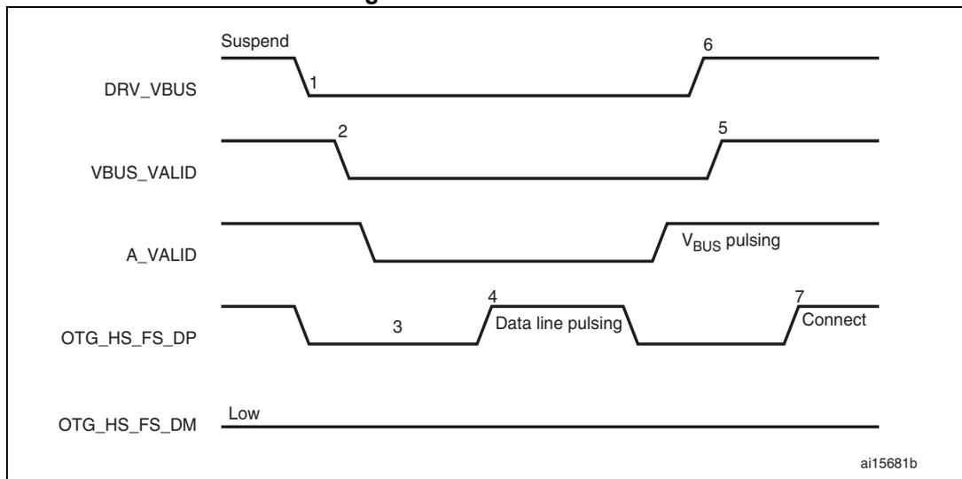
- 1. DRV_VBUS =
\(
V_{BUS}
\)
drive signal to the PHY
VBUS_VALID = \( V_{BUS} \) valid signal from PHY
A_VALID = A-device \( V_{BUS} \) level signal to PHY
DP = Data plus line
DM = Data minus line
- 1. To save power, the application suspends and turns off port power when the bus is idle by writing the port suspend and port power bits in the host port control and status register.
- 2. PHY indicates port power off by deasserting the VBUS_VALID signal.
- 3. The device must detect SE0 for at least 2 ms to start SRP when V BUS power is off.
- 4. To initiate SRP, the device turns on its data line pull-up resistor for 5 to 10 ms. The OTG_HS controller detects data-line pulsing.
- 5. The device drives V
BUS
above the A-device session valid (2.0 V minimum) for V
BUS
pulsing.
The OTG_HS controller interrupts the application on detecting SRP. The Session request detected bit is set in Global interrupt status register (SRQINT set in OTG_HS_GINTSTS). - 6. The application must service the Session request detected interrupt and turn on the port power bit by writing the port power bit in the host port control and status register. The PHY indicates port power-on by asserting the VBUS_VALID signal.
- 7. When the USB is powered, the device connects, completing the SRP process.
B-device session request protocol
The application must set the SRP-capable bit in the Core USB configuration register. This enables the OTG_HS controller to initiate SRP as a B-device. SRP is a means by which the OTG_HS controller can request a new session from the host.
Figure 431. B-device SRP
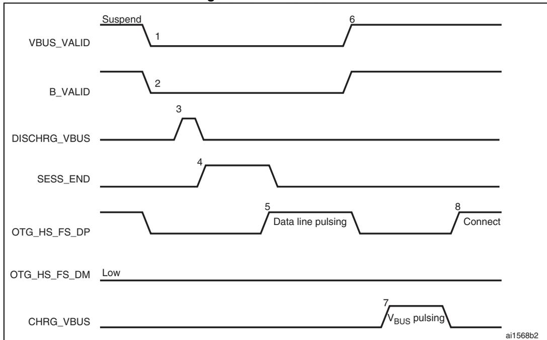
The timing diagram illustrates the signal states for B-device SRP. The signals are:
- VBUS_VALID : Starts high (Suspend), goes low at point 1, and returns high at point 6.
- B_VALID : Starts high, goes low at point 2, and returns high at point 6.
- DISCHRG_VBUS : Shows a pulse at point 3.
- SESS_END : Goes high at point 4 and returns low at point 5.
- OTG_HS_FS_DP : Shows 'Data line pulsing' between points 5 and 8, ending with 'Connect' at point 8.
- OTG_HS_FS_DM : Remains 'Low' throughout the sequence.
- CHRG_VBUS : Shows a pulse labeled 'V BUS pulsing' at point 7.
- 1. VBUS_VALID = V BUS valid signal from PHY
- 2. B_VALID = B-device valid session to PHY
- 3. DISCHRG_VBUS = discharge signal to PHY
- 4. SESS_END = session end signal to PHY
- 5. CHRG_VBUS = charge V BUS signal to PHY
- 6. DP = Data plus line
- 7. DM = Data minus line
- 8. Connect
- 1. To save power, the host suspends and turns off port power when the bus is idle.
The OTG_HS controller sets the early suspend bit in the Core interrupt register after 3 ms of bus idleness. Following this, the OTG_HS controller sets the USB suspend bit in the Core interrupt register.
The OTG_HS controller informs the PHY to discharge \( V_{BUS} \) . - 2. The PHY indicates the session's end to the device. This is the initial condition for SRP. The OTG_HS controller requires 2 ms of SE0 before initiating SRP.
For a USB 1.1 full-speed serial transceiver, the application must wait until \( V_{BUS} \) discharges to 0.2 V after BSVLD (in OTG_HS_GOTGCTL) is deasserted. This discharge time can be obtained from the transceiver vendor and varies from one transceiver to another. - 3. The USB OTG core informs the PHY to speed up \( V_{BUS} \) discharge.
- 4. The application initiates SRP by writing the session request bit in the OTG Control and status register. The OTG_HS controller perform data-line pulsing followed by \( V_{BUS} \) pulsing.
- 5. The host detects SRP from either the data-line or \( V_{BUS} \) pulsing, and turns on \( V_{BUS} \) . The PHY indicates \( V_{BUS} \) power-on to the device.
- 6. The OTG_HS controller performs
\(
V_{BUS}
\)
pulsing.
The host starts a new session by turning on \( V_{BUS} \) , indicating SRP success. The OTG_HS controller interrupts the application by setting the session request success status change bit in the OTG interrupt status register. The application reads the session request success bit in the OTG control and status register. - 7. When the USB is powered, the OTG_HS controller connects, completing the SRP process.
A-device host negotiation protocol
HNP switches the USB host role from the A-device to the B-device. The application must set the HNP-capable bit in the Core USB configuration register to enable the OTG_HS controller to perform HNP as an A-device.
Figure 432. A-device HNP
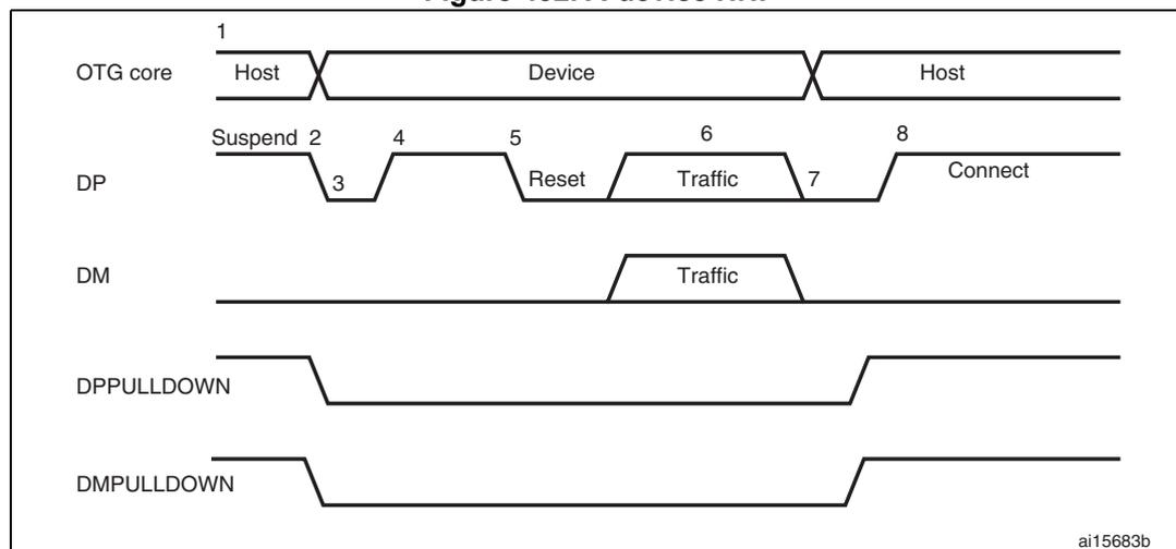
The diagram illustrates the timing for A-device HNP. It shows five signal lines over time, divided into three phases: Host, Device, and Host. The OTG core signal shows a transition from Host to Device at point 1, and back to Host at point 2. The DP signal shows a Suspend state (point 2), a Reset state (point 3), a Traffic state (point 4), a Reset state (point 5), a Traffic state (point 6), a Connect state (point 7), and a Host state (point 8). The DM signal shows a Traffic state (point 6). The DPPULLDOWN and DMPULLDOWN signals show a transition from High to Low at point 1, and back to High at point 2.
- 1. DPPULLDOWN = signal from core to PHY to enable/disable the pull-down on the DP line inside the PHY.
DMPULLDOWN = signal from core to PHY to enable/disable the pull-down on the DM line inside the PHY.
- 1. The OTG_HS controller sends the B-device a SetFeature b_hnp_enable descriptor to enable HNP support. The B-device's ACK response indicates that the B-device supports HNP. The application must set host Set HNP Enable bit in the OTG Control and status register to indicate to the OTG_HS controller that the B-device supports HNP.
- 2. When it has finished using the bus, the application suspends by writing the Port suspend bit in the host port control and status register.
- 3. When the B-device observes a USB suspend, it disconnects, indicating the initial condition for HNP. The B-device initiates HNP only when it must switch to the host role; otherwise, the bus continues to be suspended.
The OTG_HS controller sets the host negotiation detected interrupt in the OTG interrupt status register, indicating the start of HNP.
The OTG_HS controller deasserts the DM pull down and DM pull down in the PHY to indicate a device role. The PHY enables the OTG_HS_DP pull-up resistor to indicate a connect for B-device.
The application must read the current mode bit in the OTG Control and status register to determine peripheral mode operation.
- 4. The B-device detects the connection, issues a USB reset, and enumerates the OTG_HS controller for data traffic.
- 5. The B-device continues the host role, initiating traffic, and suspends the bus when done.
The OTG_HS controller sets the early suspend bit in the Core interrupt register after 3 ms of bus idleness. Following this, the OTG_HS controller sets the USB Suspend bit in the Core interrupt register.
- 6. In Negotiated mode, the OTG_HS controller detects the suspend, disconnects, and switches back to the host role. The OTG_HS controller asserts the DM pull down and DM pull down in the PHY to indicate its assumption of the host role.
- 7. The OTG_HS controller sets the Connector ID status change interrupt in the OTG Interrupt Status register. The application must read the connector ID status in the OTG Control and Status register to determine the OTG_HS controller operation as an A-device. This indicates the completion of HNP to the application. The application must read the Current mode bit in the OTG control and status register to determine host mode operation.
- 8. The B-device connects, completing the HNP process.
B-device host negotiation protocol
HNP switches the USB host role from B-device to A-device. The application must set the HNP-capable bit in the Core USB configuration register to enable the OTG_HS controller to perform HNP as a B-device.
Figure 433. B-device HNP
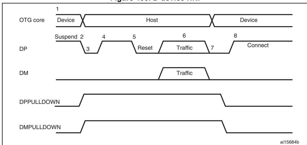
ai15684b
- 1. DPPULLDOWN = signal from core to PHY to enable/disable the pull-down on the DP line inside the PHY.
DMPULLDOWN = signal from core to PHY to enable/disable the pull-down on the DM line inside the PHY. - 1. The A-device sends the SetFeature b_hnp_enable descriptor to enable HNP support. The OTG_HS controller's ACK response indicates that it supports HNP. The application must set the Device HNP enable bit in the OTG Control and status register to indicate HNP support.
The application sets the HNP request bit in the OTG Control and status register to indicate to the OTG_HS controller to initiate HNP.
- 2. When it has finished using the bus, the A-device suspends by writing the Port suspend bit in the host port control and status register.
The OTG_HS controller sets the Early suspend bit in the Core interrupt register after 3 ms of bus idleness. Following this, the OTG_HS controller sets the USB suspend bit in the Core interrupt register.
The OTG_HS controller disconnects and the A-device detects SE0 on the bus, indicating HNP. The OTG_HS controller asserts the DP pull down and DM pull down in the PHY to indicate its assumption of the host role.
The A-device responds by activating its OTG_HS_DP pull-up resistor within 3 ms of detecting SE0. The OTG_HS controller detects this as a connect.
The OTG_HS controller sets the host negotiation success status change interrupt in the OTG Interrupt status register, indicating the HNP status. The application must read the host negotiation success bit in the OTG Control and status register to determine
host negotiation success. The application must read the current Mode bit in the Core interrupt register (OTG_HS_GINTSTS) to determine host mode operation.
- 3. The application sets the reset bit (PRST in OTG_HS_HPRT) and the OTG_HS controller issues a USB reset and enumerates the A-device for data traffic.
- 4. The OTG_HS controller continues the host role of initiating traffic, and when done, suspends the bus by writing the Port suspend bit in the host port control and status register.
- 5. In Negotiated mode, when the A-device detects a suspend, it disconnects and switches back to the host role. The OTG_HS controller deasserts the DP pull down and DM pull down in the PHY to indicate the assumption of the device role.
- 6. The application must read the current mode bit in the Core interrupt (OTG_HS_GINTSTS) register to determine the host mode operation.
- 7. The OTG_HS controller connects, completing the HNP process.