25. Hash processor (HASH)
This section applies to STM32F415/417xx and STM32F43xxx devices.
25.1 HASH introduction
The hash processor is a fully compliant implementation of the secure hash algorithm (SHA-1, SHA-224, SHA-256), the MD5 (message-digest algorithm 5) hash algorithm and the HMAC (keyed-hash message authentication code) algorithm suitable for a variety of applications. It computes a message digest (160 bits for the SHA-1 algorithm, 256 bits for the SHA-256 algorithm and 224 bits for the SHA-224 algorithm, 128 bits for the MD5 algorithm) for messages of up to \( (2^{64} - 1) \) bits, while HMAC algorithms provide a way of authenticating messages by means of hash functions. HMAC algorithms consist in calling the SHA-1, SHA-224, SHA-256 or MD5 hash function twice.
25.2 HASH main features
- • Suitable for data authentication applications, compliant with:
- – FIPS PUB 180-2 (Federal Information Processing Standards Publication 180-2)
- – Secure Hash Standard specifications (SHA-1, SHA-224 and SHA-256)
- – IETF RFC 1321 (Internet Engineering Task Force Request For Comments number 1321) specifications (MD5)
- • Fast computation of SHA-1, SHA-224 and SHA-256, and MD5 (SHA-224 and SHA-256 are available on STM32F43xxx only)
- • AHB slave peripheral
- • 32-bit data words for input data, supporting word, half-word, byte and bit bit-string representations, with little-endian data representation only.
- • Automatic swapping to comply with the big-endian SHA1, SHA-224 and SHA-256 computation standard with little-endian input bit-string representation
- • Automatic padding to complete the input bit string to fit modulo 512 ( \( 16 \times 32 \) bits) message digest computing
- • \( 5 \times 32 \) -bit words (H0 to H5) on STM32F415/417xx and \( 8 \times 32 \) -bit words (H0 to H7) on STM32F43xxx for output message digest, reload able to continue interrupted message digest computation.
- • Corresponding 32-bit words of the digest from consecutive message blocks are added to each other to form the digest of the whole message
- • Automatic data flow control with support for direct memory access (DMA)
Note: Padding, as defined in the SHA-1, SHA-224 and SHA-256 algorithm, consists in adding a bit at bx1 followed by N bits at bx0 to get a total length congruent to 448 modulo 512. After this, the message is completed with a 64-bit integer which is the binary representation of the original message length. For this hash processor, the quanta for entering the message is a 32-bit word, so an additional information must be provided at the end of the message entry, which is the number of valid bits in the last 32-bit word entered.
25.3 HASH functional description
Figure 1 shows the block diagram of the hash processor.
Figure 233. Block diagram for STM32F415/417xx
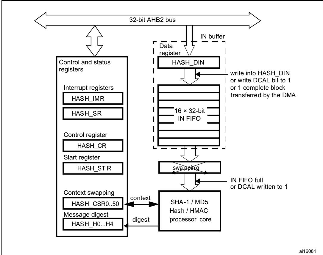
The diagram illustrates the internal architecture of the hash processor. At the top, a horizontal double-headed arrow represents the 32-bit AHB2 bus . Below it, a vertical stack of components is shown. On the left, a large box labeled Control and status registers contains several sub-registers: Interrupt registers (HASH_IMR, HASH_SR), Control register (HASH_CR), Start register (HASH_STR), Context swapping (HASH_CSR0..50), and Message digest (HASH_H0..H4). This box is connected to the bus via a double-headed arrow. To the right of the control registers, a dashed box labeled IN buffer contains a Data register (HASH_DIN) and a 16 × 32-bit IN FIFO . The HASH_DIN register is connected to the bus and receives data from an external source, indicated by an arrow pointing into it with the text: "write into HASH_DIN or write DCAL bit to 1 or 1 complete block transferred by the DMA". The IN FIFO is connected to the HASH_DIN register and to a swapping block below it. The swapping block is connected to the SHA-1 / MD5 Hash / HMAC processor core . An arrow points from the swapping block to the core with the text: "IN FIFO full or DCAL written to 1". The core sends a digest back to the Message digest register (HASH_H0..H4) and exchanges context information with the Context swapping register (HASH_CSR0..50). The identifier ai16081 is located in the bottom right corner of the diagram.
Figure 234. Block diagram for STM32F43xxx
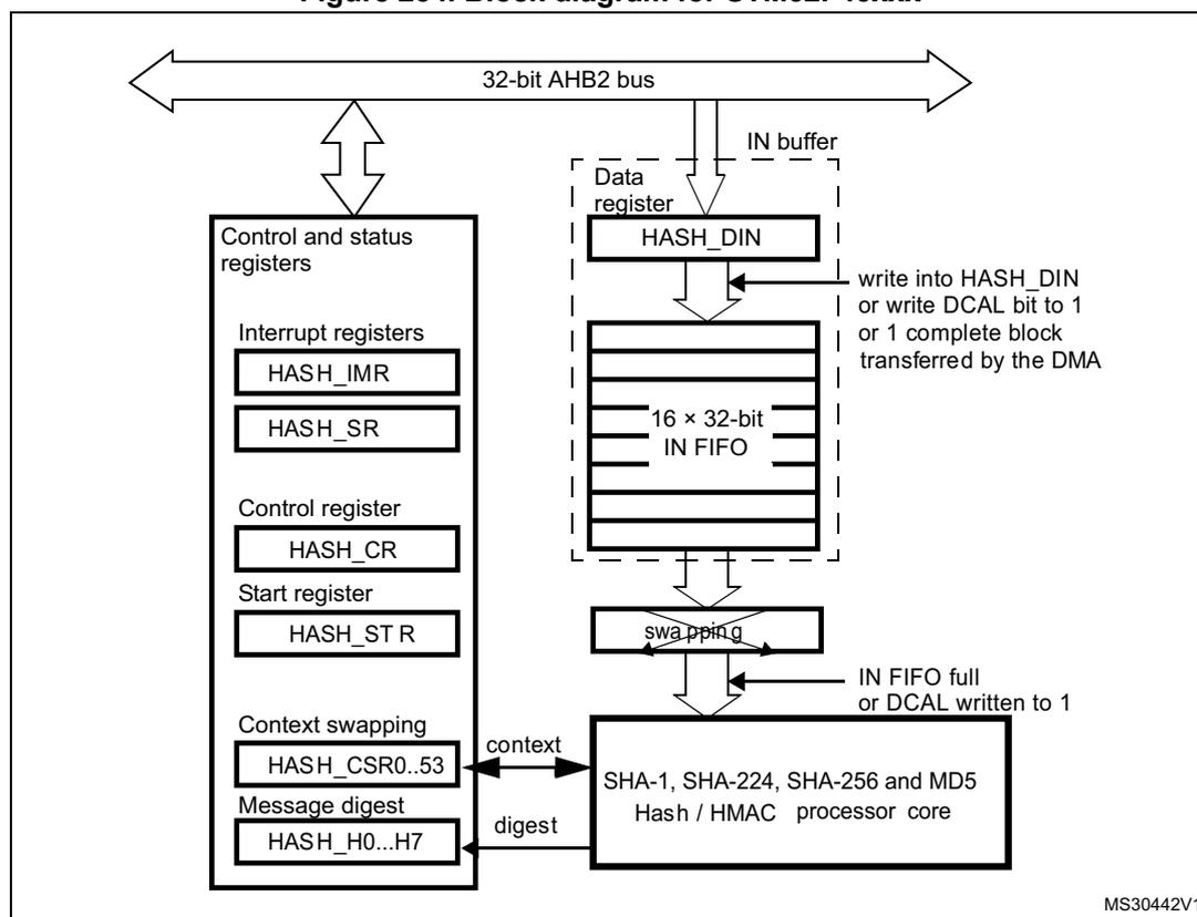
The diagram illustrates the internal architecture of the hash processor. At the top, a horizontal double-headed arrow represents the 32-bit AHB2 bus . Below this bus, on the left, is a large box labeled Control and status registers . This box contains several sub-registers: Interrupt registers (HASH_IMR, HASH_SR), Control register (HASH_CR), Start register (HASH_STR), Context swapping (HASH_CSR0..53), and Message digest (HASH_H0..H7). To the right of the bus is an IN buffer (dashed box) containing a Data register (HASH_DIN) and a 16 × 32-bit IN FIFO . An arrow points from the text "write into HASH_DIN or write DCAL bit to 1 or 1 complete block transferred by the DMA" to the HASH_DIN register. Below the IN FIFO is a swapping block. An arrow points from the text "IN FIFO full or DCAL written to 1" to this swapping block. At the bottom right is the SHA-1, SHA-224, SHA-256 and MD5 Hash / HMAC processor core . Arrows show data flow: from the IN FIFO through the swapping block to the processor core, from the core to the Message digest (HASH_H0..H7) labeled "digest", and from the Context swapping (HASH_CSR0..53) to the core labeled "context". The Control and status registers are connected to the 32-bit AHB2 bus via a vertical double-headed arrow.
MS30442V1
The FIPS PUB 180-2 standard and the IETF RFC 1321 publication specify the SHA-1, SHA-224 and SHA-256 and MD5 secure hash algorithms, respectively, for computing a condensed representation of a message or data file. When a message of any length below \( 2^{64} \) bits is provided on input, the SHA-1, SHA-224 and SHA-256 and MD5 produce respective a 160-bit, 224 bit, 256 bit and 128-bit output string, respectively, called a message digest. The message digest can then be processed with a digital signature algorithm in order to generate or verify the signature for the message. Signing the message digest rather than the message often improves the efficiency of the process because the message digest is usually much smaller in size than the message. The verifier of a digital signature has to use the same hash algorithm as the one used by the creator of the digital signature.
The SHA-1, SHA-224 and SHA-256 and MD5 are qualified as “secure” because it is computationally infeasible to find a message that corresponds to a given message digest, or to find two different messages that produce the same message digest. Any change to a message in transit, with very high probability, results in a different message digest, and the signature fails to verify. For more detail on the SHA-1 or SHA-224 and SHA-256 algorithm, please refer to the FIPS PUB 180-2 (Federal Information Processing Standards Publication 180-2), 2002 august 1.
The current implementation of this standard works with little-endian input data convention. For example, the C string “abc” must be represented in memory as the 24-bit hexadecimal value 0x434241.
A message or data file to be processed by the hash processor should be considered a bit string. The length of the message is the number of bits in the message (the empty message
has length 0). You can consider that 32 bits of this bit string forms a 32-bit word. Note that the FIPS PUB 180-1 standard uses the convention that bit strings grow from left to right, and bits can be grouped as bytes (8 bits) or words (32 bits) (but some implementations also use half-words (16 bits), and implicitly, uses the big-endian byte (half-word) ordering. This convention is mainly important for padding (see Section 1.3.4: Message padding on page 12 ).
25.3.1 Duration of the processing
The computation of an intermediate block of a message takes:
- • 66 HCLK clock cycles in SHA-1
- • 50 HCLK clock cycles in SHA-224
- • 50 HCLK clock cycles in SHA-256
- • 50 HCLK clock cycles in MD5
to which you must add the time needed to load the 16 words of the block into the processor (at least 16 clock cycles for a 512-bit block).
The time needed to process the last block of a message (or of a key in HMAC) can be longer. This time depends on the length of the last block and the size of the key (in HMAC mode). Compared to the processing of an intermediate block, it can be increased by a factor of:
- • 1 to 2.5 for a hash message
- • around 2.5 for an HMAC input-key
- • 1 to 2.5 for an HMAC message
- • around 2.5 for an HMAC output key in case of a short key
- • 3.5 to 5 for an HMAC output key in case of a long key
25.3.2 Data type
Data are entered into the hash processor 32 bits (word) at a time, by writing them into the HASH_DIN register. But the original bit-string can be organized in bytes, half-words or words, or even be represented as bits. As the system memory organization is little-endian and SHA1, SHA-224 and SHA-256 computation is big-endian, depending on the way the original bit string is grouped, a bit, byte, or half-word swapping operation is performed automatically by the hash processor.
The kind of data to be processed is configured with the DATATYPE bitfield in the HASH control register (HASH_CR).
Figure 235. Bit, byte and half-word swapping
A-In case of binary data hash, all bits should be swapped as below
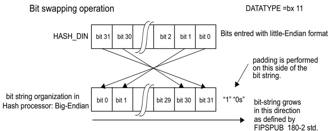
Bit swapping operation
DATATYPE =bx 11
HASH_DIN
bit 31 bit 30 ... bit 2 bit 1 bit 0
Bits entered with little-Endian format
bit string organization in Hash processor: Big-Endian
bit 0 bit 1 ... bit 29 bit 30 bit 31
"1" "0s"
padding is performed on this side of the bit string.
bit-string grows in this direction as defined by FIPSPUB 180-2 std.
B-In case of byte data hash, all bytes should be swapped as below
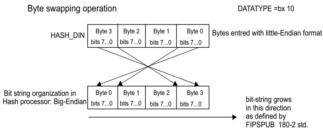
Byte swapping operation
DATATYPE =bx 10
HASH_DIN
Byte 3 bits 7...0 Byte 2 bits 7...0 Byte 1 bits 7...0 Byte 0 bits 7...0
Bytes entered with little-Endian format
Bit string organization in Hash processor: Big-Endian
Byte 0 bits 7...0 Byte 1 bits 7...0 Byte 2 bits 7...0 Byte 3 bits 7...0
bit-string grows in this direction as defined by FIPSPUB 180-2 std.
C-In case of half-word hash, all half-word should be swapped as below
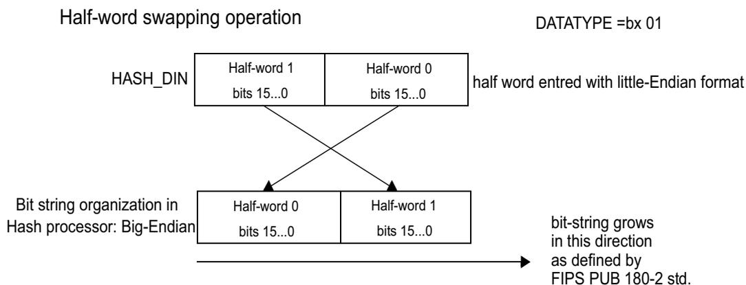
Half-word swapping operation
DATATYPE =bx 01
HASH_DIN
Half-word 1 bits 15...0 Half-word 0 bits 15...0
half word entered with little-Endian format
Bit string organization in Hash processor: Big-Endian
Half-word 0 bits 15...0 Half-word 1 bits 15...0
bit-string grows in this direction as defined by FIPS PUB 180-2 std.
ai16082b
The least significant bit of the message has to be at position 0 (right) in the first word entered into the hash processor, the 32nd bit of the bit string has to be at position 0 in the second word entered into the hash processor and so on.
25.3.3 Message digest computing
The HASH sequentially processes blocks of 512 bits when computing the message digest. Thus, each time \( 16 \times 32 \) -bit words ( \( = 512 \) bits) have been written by the DMA or the CPU, into the hash processor, the HASH automatically starts computing the message digest. This operation is known as a partial digest computation.
The message to be processed is entered into the peripheral by 32-bit words written into the HASH_DIN register. The current contents of the HASH_DIN register are transferred to the input FIFO (IN FIFO) each time the register is written with new data. HASH_DIN and the input FIFO form a FIFO of a 17-word length (named the IN buffer).
The processing of a block can start only once the last value of the block has entered the IN FIFO. The peripheral must get the information as to whether the HASH_DIN register contains the last bits of the message or not. Two cases may occur:
- • When the DMA is not used:
- – In case of a partial digest computation, this is done by writing an additional word into the HASH_DIN register (actually the first word of the next block). Then the software must wait until the processor is ready again (when DINIS=1) before writing new data into HASH_DIN.
- – In case of a final digest computation (last block entered), this is done by writing the DCAL bit to 1.
- • When the DMA is used:
The contents of the HASH_DIN register are interpreted automatically with the information sent by the DMA controller.
- – In case of a single DMA transfer: Multiple DMA transfer (MDMAT) bit should be cleared on STM32F43xxx. When the last block has been transferred to the HASH_DIN register via DMA channel, DCAL bit is set to automatically to 1 in the HASH_STR register in order to launch the final digest calculation.
- – In case of a multiple DMA transfer (available only on STM32F43xxx): Multiple DMA transfer (MDMAT) bit should be set to 1 by software so DCAL bit does not get set automatically by HW, in this case the final digest calculation for hash and for each phases for HMAC (for more details about HMAC phases please refer to HMAC operation section) is not launched at the end of the DMA transfer request, allowing the processor to receive a new DMA transfer. During the last DMA transfer, Multiple DMA transfer (MDMAT) bit should be cleared by software in order to set automatically DCAL bit at the end of the last block and launch the final digest.
- – The contents of the HASH_DIN register are interpreted automatically with the information sent by the DMA controller.
This process —data entering + partial digest computation— continues until the last bits of the original message are written to the HASH_DIN register. As the length (number of bits) of a message can be any integer value, the last word written into the HASH processor may have a valid number of bits between 1 and 32. This number of valid bits in the last word, NBLW, has to be written into the HASH_STR register, so that message padding is correctly performed before the final message digest computation.
Once this is done, writing into HASH_STR with bit DCAL = 1 starts the processing of the last entered block of message by the hash processor. This processing consists in:
- • Automatically performing the message padding operation: the purpose of this operation is to make the total length of a padded message a multiple of 512. The HASH sequentially processes blocks of 512 bits when computing the message digest
- • Computing the final message digest
When the DMA is enabled, it provides the information to the hash processor when it is transferring the last data word. Then the padding and digest computation are performed automatically as if DCAL had been written to 1.
25.3.4 Message padding
Message padding consists in appending a “1” followed by m “0”s followed by a 64-bit integer to the end of the original message to produce a padded message block of length 512. The “1” is added to the last word written into the HASH_DIN register at the bit position defined by the NBLW bitfield, and the remaining upper bits are cleared (“0”s).
Example: let us assume that the original message is the ASCII binary-coded form of “abc”, of length L = 24:
byte 0      byte 1      byte 2      byte 3
01100001 01100010 01100011 UUUUUUUU
<-- 1st word written to HASH_DIN -->
NBLW has to be loaded with the value 24: a “1” is appended at bit location 24 in the bit string (starting counting from left to right in the above bit string), which corresponds to bit 31 in the HASH_DIN register (little-endian convention):
01100001 01100010 01100011 1UUUUUUU
Since L = 24, the number of bits in the above bit string is 25, and 423 “0”s are appended, making now 448. This gives (in hexadecimal, big-endian format):
61626380 00000000 00000000 00000000
00000000 00000000 00000000 00000000
00000000 00000000 00000000 00000000
00000000 00000000
The L value, in two-word representation (that is 00000000 00000018) is appended. Hence the final padded message in hexadecimal:
61626380 00000000 00000000 00000000
00000000 00000000 00000000 00000000
00000000 00000000 00000000 00000000
00000000 00000000 00000000 00000028
If the HASH is programmed to use the little-endian byte input format, the above message has to be entered by doing the following steps:
- 1. 0xUU636261 is written into the HASH_DIN register (where ‘U’ means don’t care)
- 2. 0x18 is written into the HASH_STR register (the number of valid bits in the last word written into the HASH_DIN register is 24, as the original message length is 24 bits)
- 3. 0x10 is written into the HASH_STR register to start the message padding and digest computation. When NBLW ≠ 0x00, the message padding puts a “1” into the HASH_DIN register at the bit position defined by the NBLW value, and inserts “0”s at bit locations [31:(NBLW+1)]. When NBLW == 0x00, the message padding inserts one new word with
value 0x0000 0001. Then an all zero word (0x0000 0000) is added and the message length in a two-word representation, to get a block of 16 x 32-bit words.
- 4. The HASH computing is performed, and the message digest is then available in the HASH_Hx registers (x = 0...4) for the SHA-1 algorithm. For example:
H0 = 0xA9993E36
H1 = 0x4706816A
H2 = 0xBA3E2571
H3 = 0x7850C26C
H4 = 0x9CD0D89D
25.3.5 Hash operation
The hash function (SHA-1, SHA-224, SHA-256 and MD5) is selected when the INIT bit is written to '1' in the HASH_CR register while the MODE bit is at '0' in HASH_CR. The algorithm (SHA-1, SHA-224, SHA-256 or MD5) is selected at the same time (that is when the INIT bit is set) using the ALGO bits.
The message can then be sent by writing it word by word into the HASH_DIN register. When a block of 512 bits—that is 16 words—has been written, a partial digest computation starts upon writing the first data of the next block. The hash processor remains busy for 66 cycles for the SHA-1 algorithm, or 50 cycles for the MD5 algorithm, SHA-224 algorithm and SHA-256 algorithm.
The process can then be repeated until the last word of the message. If DMA transfers are used, refer to the Procedure where the data are loaded by DMA section. Otherwise, if the message length is not an exact multiple of 512 bits, then the HASH_STR register has to be written to launch the computation of the final digest.
Once computed, the digest can be read from the HASH_H0...HASH_H4 registers (for the MD5 algorithm, HASH_H4 is not relevant) on STM32F415/417xx, and from the HASH_H0...HASH_H7 registers on STM32F43xxx where:
HASH_H4..HASH_H7 are not relevant when the MD5 algorithm is selected,
HASH_H5.. HASH_H7 are not relevant when the SHA-1 algorithm is selected,
HASH_H7 is not relevant when the SHA-224 algorithm is selected.
25.3.6 HMAC operation
The HMAC algorithm is used for message authentication, by irreversibly binding the message being processed to a key chosen by the user. For HMAC specifications, refer to “HMAC: keyed-hashing for message authentication, H. Krawczyk, M. Bellare, R. Canetti, February 1997.
Basically, the algorithm consists of two nested hash operations:
where:
- • pad is a sequence of zeroes needed to extend the key to the length of the underlying hash function data block (that is 512 bits for both the SHA-1, SHA224, SHA-256 and MD5 hash algorithms)
- • | represents the concatenation operator
To compute the HMAC, four different phases are required:
- 1. The block is initialized by writing the INIT bit to '1' with the MODE bit at '1' and the ALGO bits set to the value corresponding to the desired algorithm. The LKEY bit must also be set during this phase if the key being used is longer than 64 bytes (in this case, the HMAC specifications specify that the hash of the key should be used in place of the real key).
- 2. The key (to be used for the inner hash function) is then given to the core. This operation follows the same mechanism as the one used to send the message in the hash operation (that is, by writing into HASH_DIN and, finally, into HASH_STR).
- 3. Once the last word has been entered and computation has started, the hash processor elaborates the key. It is then ready to accept the message text using the same mechanism as the one used to send the message in the hash operation.
- 4. After the first hash round, the hash processor returns "ready" to indicate that it is ready to receive the key to be used for the outer hash function (normally, this key is the same as the one used for the inner hash function). When the last word of the key is entered and computation starts, the HMAC result is made available in the HASH_H0...HASH_H4 registers on STM32F415/417xx and on HASH_H0...HASH_H7 registers on STM32F43xxx.
Note: 1 The computation latency of the HMAC primitive depends on the lengths of the keys and message. You could the HMAC as two nested underlying hash functions with the same key length (long or short).
25.3.7 Context swapping
It is possible to interrupt a hash/HMAC process to perform another processing with a higher priority, and to complete the interrupted process later on, when the higher-priority task is complete. To do so, the context of the interrupted task must be saved from the hash registers to memory, and then be restored from memory to the hash registers.
The procedures where the data flow is controlled by software or by DMA are described below.
Procedure where the data are loaded by software
The context can be saved only when no block is currently being processed. That is, you must wait for DINIS = 1 (the last block has been processed and the input FIFO is empty) or NBW ≠ 0 (the FIFO is not full and no processing is ongoing).
- Context saving:
Store the contents of the following registers into memory:
- – HASH_IMR
- – HASH_STR
- – HASH_CR
- – HASH_CSR0 to HASH_CSR50 on STM32F415/417xx, and HASH_CSR0 to HASH_CSR53 on STM32F43xxx.
- Context restoring:
The context can be restored when the high-priority task is complete. Please follow the order of the sequence below.
- Write the following registers with the values saved in memory: HASH_IMR, HASH_STR and HASH_CR
- Initialize the hash processor by setting the INIT bit in the HASH_CR register
- Write the HASH_CSR0 to HASH_CSR50 (STM32F415/417xx), and HASH_CSR0 to HASH_CSR53 (STM32F43xxx) registers with the values saved in memory
You can now restart the processing from the point where it has been interrupted.
Procedure where the data are loaded by DMA
In this case it is not possible to predict if a DMA transfer is in progress or if the process is ongoing. Thus, you must stop the DMA transfers, then wait until the HASH is ready in order to interrupt the processing of a message.
- Interrupting a processing:
- – Clear the DMAE bit to disable the DMA interface
- – Wait until the current DMA transfer is complete (wait for DMAES = 0 in the HASH_SR register). Note that the block may or not have been totally transferred to the HASH.
- – Disable the corresponding channel in the DMA controller
- – Wait until the hash processor is ready (no block is being processed), that is wait for DINIS = 1
- The context saving and context restoring phases are the same as above (see Procedure where the data are loaded by software ).
Reconfigure the DMA controller so that it transfers the end of the message. You can now restart the processing from the point where it was interrupted by setting the DMAE bit.
Note: If context swapping does not involve HMAC operations, the HASH_CSR38 to HASH_CSR50 (STM32F415/417xx) and HASH_CSR38 to HASH_CSR53 (STM32F43xxx) registers do not have to be saved and restored.
If context swapping occurs between two blocks (the last block was completely processed and the next block has not yet been pushed into the IN FIFO, NBW = 000 in the HASH_CR register), the HASH_CSR22 to HASH_CSR37 registers do not have to be saved and restored.
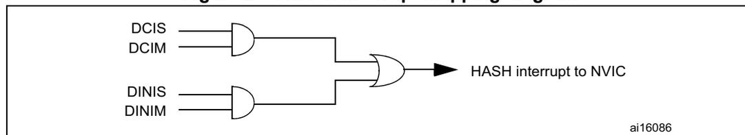
25.3.8 HASH interrupt
There are two individual maskable interrupt sources generated by the HASH processor. They are connected to the same interrupt vector.
You can enable or disable the interrupt sources individually by changing the mask bits in the HASH_IMR register. Setting the appropriate mask bit to 1 enables the interrupt.
The status of the individual interrupt sources can be read from the HASH_SR register.
Figure 236. HASH interrupt mapping diagram
25.4 HASH registers
The HASH core is associated with several control and status registers and five message digest registers.
All these registers are accessible through word accesses only, else an AHB error is generated.
25.4.1 HASH control register (HASH_CR) for STM32F415/417xx
Address offset: 0x00
Reset value: 0x0000 0000
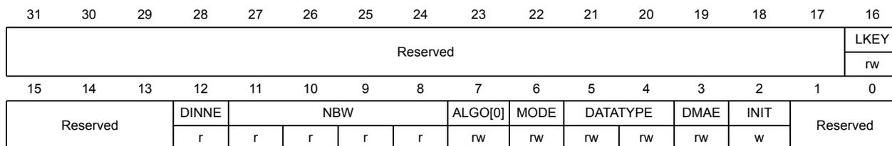
| 31 | 30 | 29 | 28 | 27 | 26 | 25 | 24 | 23 | 22 | 21 | 20 | 19 | 18 | 17 | 16 |
| Reserved | LKEY | ||||||||||||||
| rw | |||||||||||||||
| 15 | 14 | 13 | 12 | 11 | 10 | 9 | 8 | 7 | 6 | 5 | 4 | 3 | 2 | 1 | 0 |
| Reserved | DINNE | NBW | ALGO[0] | MODE | DATATYPE | DMAE | INIT | Reserved | |||||||
| r | r | rw | rw | rw | rw | w | |||||||||
Bits 31:17 Reserved, forced by hardware to 0.
Bit 16 LKEY : Long key selection
This bit selects between short key ( \( \leq 64 \) bytes) or long key ( \( > 64 \) bytes) in HMAC mode
0: Short key ( \( \leq 64 \) bytes)
1: Long key ( \( > 64 \) bytes)
Note: This selection is only taken into account when the INIT bit is set and MODE = 1. Changing this bit during a computation has no effect.
Bits 15:13 Reserved, forced by hardware to 0.
Bit 12 DINNE : DIN not emptyThis bit is set when the HASH_DIN register holds valid data (that is after being written at least once). It is cleared when either the INIT bit (initialization) or the DCAL bit (completion of the previous message processing) is written to 1.
0: No data are present in the data input buffer
1: The input buffer contains at least one word of data
Bits 11:8 NBW : Number of words already pushedThis bitfield reflects the number of words in the message that have already been pushed into the IN FIFO.
NBW increments (+1) when a write access is performed to the HASH_DIN register while DINNE = 1.
It goes to 0000 when the INIT bit is written to 1 or when a digest calculation starts (DCAL written to 1 or DMA end of transfer).
" If the DMA is not used:
0000 and DINNE=0: no word has been pushed into the DIN buffer (the buffer is empty, both the HASH_DIN register and the IN FIFO are empty)
0000 and DINNE=1: 1 word has been pushed into the DIN buffer (The HASH_DIN register contains 1 word, the IN FIFO is empty)
0001: 2 words have been pushed into the DIN buffer (the HASH_DIN register and the IN FIFO contain 1 word each)
...
1111: 16 words have been pushed into the DIN buffer
" If the DMA is used, NBW is the exact number of words that have been pushed into the IN FIFO.
Bit 7 ALGO[1:0] : Algorithm selectionThese bits select the SHA-1 or the MD5 algorithm:
0: SHA-1 algorithm selected
1: MD5 algorithm selected
Note: This selection is only taken into account when the INIT bit is set. Changing this bit during a computation has no effect.
Bit 6 MODE : Mode selectionThis bit selects the HASH or HMAC mode for the selected algorithm:
0: Hash mode selected
1: HMAC mode selected. LKEY must be set if the key being used is longer than 64 bytes.
Note: This selection is only taken into account when the INIT bit is set. Changing this bit during a computation has no effect.
Bits 5:4 DATATYPE : Data type selectionDefines the format of the data entered into the HASH_DIN register:
00: 32-bit data. The data written into HASH_DIN are directly used by the HASH processing, without reordering.
01: 16-bit data, or half-word. The data written into HASH_DIN are considered as 2 half-words, and are swapped before being used by the HASH processing.
10: 8-bit data, or bytes. The data written into HASH_DIN are considered as 4 bytes, and are swapped before being used by the HASH processing.
11: bit data, or bit-string. The data written into HASH_DIN are considered as 32 bits (1st bit of the string at position 0), and are swapped before being used by the HASH processing (1st bit of the string at position 31).
Bit 3 DMAE: DMA enable0: DMA transfers disabled
1: DMA transfers enabled. A DMA request is sent as soon as the HASH core is ready to receive data.
Note: 1: This bit is cleared by hardware when the DMA asserts the DMA terminal count signal (while transferring the last data of the message). This bit is not cleared when the INIT bit is written to 1.
2: If this bit is written to 0 while a DMA transfer has already been requested to the DMA, DMAE is cleared but the current transfer is not aborted. Instead, the DMA interface remains internally enabled until the transfer is complete or INIT is written to 1.
Bit 2 INIT: Initialize message digest calculationWriting this bit to 1 resets the hash processor core, so that the HASH is ready to compute the message digest of a new message.
Writing this bit to 0 has no effect.
Reading this bit always return 0.
Bits 1:0 Reserved, must be kept cleared.
25.4.2 HASH control register (HASH_CR) for STM32F43xxx
Address offset: 0x00
Reset value: 0x0000 0000
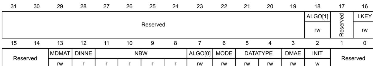
| 31 | 30 | 29 | 28 | 27 | 26 | 25 | 24 | 23 | 22 | 21 | 20 | 19 | 18 | 17 | 16 |
| Reserved | ALGO[1] | Reserved | LKEY | ||||||||||||
| rw | rw | ||||||||||||||
| 15 | 14 | 13 | 12 | 11 | 10 | 9 | 8 | 7 | 6 | 5 | 4 | 3 | 2 | 1 | 0 |
| Reserved | MDMAT | DINNE | NBW | ALGO[0] | MODE | DATATYPE | DMAE | INIT | Reserved | ||||||
| rw | r | r | r | r | r | rw | rw | rw | rw | rw | w | ||||
Bits 31:19 Reserved, forced by hardware to 0.
Bit 17 Reserved, forced by hardware to 0.
Bit 16 LKEY : Long key selection
This bit selects between short key ( \( \leq 64 \) bytes) or long key ( \( > 64 \) bytes) in HMAC mode
- 0: Short key ( \( \leq 64 \) bytes)
- 1: Long key ( \( > 64 \) bytes)
Note: This selection is only taken into account when the INIT bit is set and MODE = 1. Changing this bit during a computation has no effect.
Bits 15:14 Reserved, forced by hardware to 0.
Bit 13 MDMAT : Multiple DMA Transfers
This bit is set when hashing large files when multiple DMA transfers are needed.
- 0: DCAL is automatically set at the end of a DMA transfer.
- 1: DCAL is not automatically set at the end of a DMA transfer.
Bit 12 DINNE : DIN not empty
This bit is set when the HASH_DIN register holds valid data (that is after being written at least once). It is cleared when either the INIT bit (initialization) or the DCAL bit (completion of the previous message processing) is written to 1.
- 0: No data are present in the data input buffer
- 1: The input buffer contains at least one word of data
This bitfield reflects the number of words in the message that have already been pushed into the IN FIFO.
NBW increments (+1) when a write access is performed to the HASH_DIN register while DINNE = 1.
It goes to 0000 when the INIT bit is written to 1 or when a digest calculation starts (DCAL written to 1 or DMA end of transfer).
” If the DMA is not used:
0000 and DINNE=0: no word has been pushed into the DIN buffer (the buffer is empty, both the HASH_DIN register and the IN FIFO are empty)
0000 and DINNE=1: 1 word has been pushed into the DIN buffer (The HASH_DIN register contains 1 word, the IN FIFO is empty)
0001: 2 words have been pushed into the DIN buffer (the HASH_DIN register and the IN FIFO contain 1 word each)
...
1111: 16 words have been pushed into the DIN buffer
” If the DMA is used, NBW is the exact number of words that have been pushed into the IN FIFO.
Bit 18 and bit 7 ALGO[1:0] : Algorithm selectionThese bits selects the SHA-1, SHA-224, SHA256 or the MD5 algorithm:
00: SHA-1 algorithm selected
01: MD5 algorithm selected
10: SHA224 algorithm selected
11: SHA256 algorithm selected
Note: This selection is only taken into account when the INIT bit is set. Changing this bit during a computation has no effect.
Bit 6 MODE : Mode selectionThis bit selects the HASH or HMAC mode for the selected algorithm:
0: Hash mode selected
1: HMAC mode selected. LKEY must be set if the key being used is longer than 64 bytes.
Note: This selection is only taken into account when the INIT bit is set. Changing this bit during a computation has no effect.
Bits 5:4 DATATYPE : Data type selectionDefines the format of the data entered into the HASH_DIN register:
00: 32-bit data. The data written into HASH_DIN are directly used by the HASH processing, without reordering.
01: 16-bit data, or half-word. The data written into HASH_DIN are considered as 2 half-words, and are swapped before being used by the HASH processing.
10: 8-bit data, or bytes. The data written into HASH_DIN are considered as 4 bytes, and are swapped before being used by the HASH processing.
11: bit data, or bit-string. The data written into HASH_DIN are considered as 32 bits (1st bit of the string at position 0), and are swapped before being used by the HASH processing (1st bit of the string at position 31).
Bit 3 DMAE : DMA enable0: DMA transfers disabled
1: DMA transfers enabled. A DMA request is sent as soon as the HASH core is ready to receive data.
Note: 1: This bit is cleared by hardware when the DMA asserts the DMA terminal count signal (while transferring the last data of the message). This bit is not cleared when the INIT bit is written to 1.
2: If this bit is written to 0 while a DMA transfer has already been requested to the DMA, DMAE is cleared but the current transfer is not aborted. Instead, the DMA interface remains internally enabled until the transfer is complete or INIT is written to 1.
Bit 2 INIT : Initialize message digest calculationWriting this bit to 1 resets the hash processor core, so that the HASH is ready to compute the message digest of a new message.
Writing this bit to 0 has no effect.
Reading this bit always return 0.
Bits 1:0 Reserved, must be kept cleared.
25.4.3 HASH data input register (HASH_DIN)
Address offset: 0x04
Reset value: 0x0000 0000
HASH_DIN is the data input register. It is 32-bit wide. It is used to enter the message by blocks of 512 bits. When the HASH_DIN register is written to, the value presented on the AHB databus is 'pushed' into the HASH core and the register takes the new value presented on the AHB databus. The DATATYPE bits must previously have been configured in the HASH_CR register to get a correct message representation.
When a block of 16 words has been written to the HASH_DIN register, an intermediate digest calculation is launched:
- • by writing new data into the HASH_DIN register (the first word of the next block) if the DMA is not used (intermediate digest calculation)
- • automatically if the DMA is used
When the last block has been written to the HASH_DIN register, the final digest calculation (including padding) is launched:
- • by writing the DCAL bit to 1 in the HASH_STR register (final digest calculation)
- • automatically if the DMA is used and MDMAT bit is set to '0'.
When a digest calculation (intermediate or final) is in progress, any new write access to the HASH_DIN register is extended (by wait-state insertion on the AHB bus) until the HASH calculation completes.
When the HASH_DIN register is read, the last word written in this location is accessed (zero after reset).
| 31 | 30 | 29 | 28 | 27 | 26 | 25 | 24 | 23 | 22 | 21 | 20 | 19 | 18 | 17 | 16 |
|---|---|---|---|---|---|---|---|---|---|---|---|---|---|---|---|
| DATAIN | |||||||||||||||
| rw | rw | rw | rw | rw | rw | rw | rw | rw | rw | rw | rw | rw | rw | rw | rw |
| 15 | 14 | 13 | 12 | 11 | 10 | 9 | 8 | 7 | 6 | 5 | 4 | 3 | 2 | 1 | 0 |
| DATAIN | |||||||||||||||
| rw | rw | rw | rw | rw | rw | rw | rw | rw | rw | rw | rw | rw | rw | rw | rw |
Bits 31:0 DATAIN : Data input
Read = returns the current register content.
Write = the current register content is pushed into the IN FIFO, and the register takes the new value presented on the AHB databus.
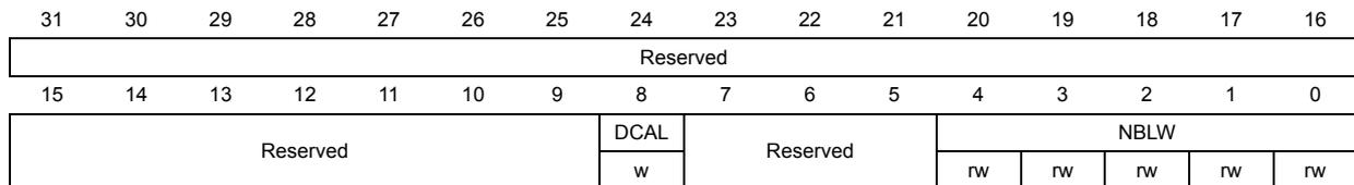
25.4.4 HASH start register (HASH_STR)
Address offset: 0x08
Reset value: 0x0000 0000
The HASH_STR register has two functions:
- • It is used to define the number of valid bits in the last word of the message entered in the hash processor (that is the number of valid least significant bits in the last data written into the HASH_DIN register)
- • It is used to start the processing of the last block in the message by writing the DCAL bit to 1
| 31 | 30 | 29 | 28 | 27 | 26 | 25 | 24 | 23 | 22 | 21 | 20 | 19 | 18 | 17 | 16 | |
| Reserved | ||||||||||||||||
| 15 | 14 | 13 | 12 | 11 | 10 | 9 | 8 | 7 | 6 | 5 | 4 | 3 | 2 | 1 | 0 | |
| Reserved | DCAL | Reserved | NBLW | |||||||||||||
| w | rw | rw | rw | rw | rw | |||||||||||
Bits 31:9 Reserved, forced by hardware to 0.
Bit 8 DCAL : Digest calculation
Writing this bit to 1 starts the message padding, using the previously written value of NBLW, and starts the calculation of the final message digest with all data words written to the IN FIFO since the INIT bit was last written to 1.
Reading this bit returns 0.
Note
Bits 7:5 Reserved, forced by hardware to 0.
Bits 4:0 NBLW : Number of valid bits in the last word of the message in the bit string organization of hash processor
When these bits are written and DCAL is at '0', they take the value on the AHB databus:
0x00: All 32 bits of the last data written in the bit string organization of hash processor (after data swapping) are valid.
0x01: Only bit [31] of the last data written in the bit string organization of hash processor (after data swapping) are valid
0x02: Only bits [31:30] of the last data written in the bit string organization of hash processor (after data swapping) are valid
0x03: Only bits [31:29] of the last data written in the bit string organization of hash processor (after data swapping) are valid
...
0x1F: Only bits [0] of the last data written in the bit string organization of hash processor (after data swapping) are valid
When these bits are written and DCAL is at '1', the bitfield is not changed.
Reading them returns the last value written to NBLW.
Note: These bits must be configured before setting the DCAL bit, else they are not taken into account. Especially, it is not possible to configure NBLW and set DCAL at the same time.
25.4.5 HASH digest registers (HASH_HR0..4/5/6/7)
Address offset: 0x0C to 0x1C (STM32F415/417xx), plus 0x310 to 0x32C (STM32F43xxx)
Reset value: 0x0000 0000
These registers contain the message digest result named as:
- 1. H0, H1, H2, H3 and H4, respectively, in the SHA1 algorithm description
Note that in this case, the HASH_H5 to HASH_H7 register is not used, and is read as zero. - 2. A, B, C and D, respectively, in the MD5 algorithm description
Note that in this case, the HASH_H4 to HASH_H7 register is not used, and is read as zero. - 3. H0 to H6, respectively, in the SHA224 algorithm description,
Note that in this case, the HASH_H7 register is not used, and is read as zero. - 4. H0 to H7, respectively, in the SHA256 algorithm description,
If a read access to one of these registers occurs while the HASH core is calculating an intermediate digest or a final message digest (that is when the DCAL bit has been written to 1), then the read is stalled until the completion of the HASH calculation.
Note: H0, H1, H2, H3 and H4 mapping are duplicated in two regions.
HASH_HR0
Address offset: 0x0C and 0x310
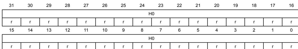
| 31 | 30 | 29 | 28 | 27 | 26 | 25 | 24 | 23 | 22 | 21 | 20 | 19 | 18 | 17 | 16 |
| H0 | |||||||||||||||
| r | r | r | r | r | r | r | r | r | r | r | r | r | r | r | r |
| 15 | 14 | 13 | 12 | 11 | 10 | 9 | 8 | 7 | 6 | 5 | 4 | 3 | 2 | 1 | 0 |
| H0 | |||||||||||||||
| r | r | r | r | r | r | r | r | r | r | r | r | r | r | r | r |
HASH_HR1
Address offset: 0x10 and 0x314
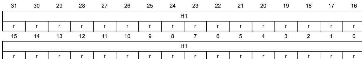
| 31 | 30 | 29 | 28 | 27 | 26 | 25 | 24 | 23 | 22 | 21 | 20 | 19 | 18 | 17 | 16 |
| H1 | |||||||||||||||
| r | r | r | r | r | r | r | r | r | r | r | r | r | r | r | r |
| 15 | 14 | 13 | 12 | 11 | 10 | 9 | 8 | 7 | 6 | 5 | 4 | 3 | 2 | 1 | 0 |
| H1 | |||||||||||||||
| r | r | r | r | r | r | r | r | r | r | r | r | r | r | r | r |
HASH_HR2
Address offset: 0x14 and 0x318

| 31 | 30 | 29 | 28 | 27 | 26 | 25 | 24 | 23 | 22 | 21 | 20 | 19 | 18 | 17 | 16 |
| H2 | |||||||||||||||
| r | r | r | r | r | r | r | r | r | r | r | r | r | r | r | r |
| 15 | 14 | 13 | 12 | 11 | 10 | 9 | 8 | 7 | 6 | 5 | 4 | 3 | 2 | 1 | 0 |
|---|---|---|---|---|---|---|---|---|---|---|---|---|---|---|---|
| H2 | |||||||||||||||
| r | r | r | r | r | r | r | r | r | r | r | r | r | r | r | r |
HASH_HR3
Address offset: 0x18 and 0x31C
| 31 | 30 | 29 | 28 | 27 | 26 | 25 | 24 | 23 | 22 | 21 | 20 | 19 | 18 | 17 | 16 |
|---|---|---|---|---|---|---|---|---|---|---|---|---|---|---|---|
| H3 | |||||||||||||||
| r | r | r | r | r | r | r | r | r | r | r | r | r | r | r | r |
| 15 | 14 | 13 | 12 | 11 | 10 | 9 | 8 | 7 | 6 | 5 | 4 | 3 | 2 | 1 | 0 |
| H3 | |||||||||||||||
| r | r | r | r | r | r | r | r | r | r | r | r | r | r | r | r |
HASH_HR4
Address offset: 0x1C and 0x320
| 31 | 30 | 29 | 28 | 27 | 26 | 25 | 24 | 23 | 22 | 21 | 20 | 19 | 18 | 17 | 16 |
|---|---|---|---|---|---|---|---|---|---|---|---|---|---|---|---|
| H4 | |||||||||||||||
| r | r | r | r | r | r | r | r | r | r | r | r | r | r | r | r |
| 15 | 14 | 13 | 12 | 11 | 10 | 9 | 8 | 7 | 6 | 5 | 4 | 3 | 2 | 1 | 0 |
| H4 | |||||||||||||||
| r | r | r | r | r | r | r | r | r | r | r | r | r | r | r | r |
HASH_HR5
Address offset: 0x324
| 31 | 30 | 29 | 28 | 27 | 26 | 25 | 24 | 23 | 22 | 21 | 20 | 19 | 18 | 17 | 16 |
|---|---|---|---|---|---|---|---|---|---|---|---|---|---|---|---|
| H5 | |||||||||||||||
| r | r | r | r | r | r | r | r | r | r | r | r | r | r | r | r |
| 15 | 14 | 13 | 12 | 11 | 10 | 9 | 8 | 7 | 6 | 5 | 4 | 3 | 2 | 1 | 0 |
| H5 | |||||||||||||||
| r | r | r | r | r | r | r | r | r | r | r | r | r | r | r | r |
HASH_HR6
Address offset: 0x328
| 31 | 30 | 29 | 28 | 27 | 26 | 25 | 24 | 23 | 22 | 21 | 20 | 19 | 18 | 17 | 16 |
|---|---|---|---|---|---|---|---|---|---|---|---|---|---|---|---|
| H6 | |||||||||||||||
| r | r | r | r | r | r | r | r | r | r | r | r | r | r | r | r |
| 15 | 14 | 13 | 12 | 11 | 10 | 9 | 8 | 7 | 6 | 5 | 4 | 3 | 2 | 1 | 0 |
| H6 | |||||||||||||||
| r | r | r | r | r | r | r | r | r | r | r | r | r | r | r | r |
HASH_HR7
Address offset: 0x32C
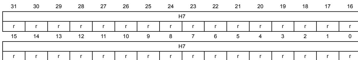
| 31 | 30 | 29 | 28 | 27 | 26 | 25 | 24 | 23 | 22 | 21 | 20 | 19 | 18 | 17 | 16 |
| H7 | |||||||||||||||
| r | r | r | r | r | r | r | r | r | r | r | r | r | r | r | r |
| 15 | 14 | 13 | 12 | 11 | 10 | 9 | 8 | 7 | 6 | 5 | 4 | 3 | 2 | 1 | 0 |
| H7 | |||||||||||||||
| r | r | r | r | r | r | r | r | r | r | r | r | r | r | r | r |
Note: When starting a digest computation for a new bit stream (by writing the INIT bit to 1), these registers assume their reset values.
25.4.6 HASH interrupt enable register (HASH_IMR)
Address offset: 0x20
Reset value: 0x0000 0000
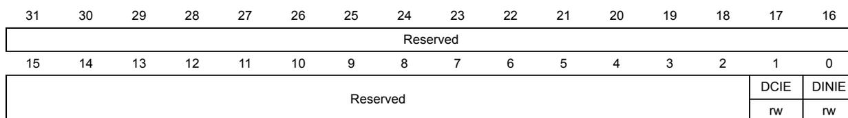
| 31 | 30 | 29 | 28 | 27 | 26 | 25 | 24 | 23 | 22 | 21 | 20 | 19 | 18 | 17 | 16 |
| Reserved | |||||||||||||||
| 15 | 14 | 13 | 12 | 11 | 10 | 9 | 8 | 7 | 6 | 5 | 4 | 3 | 2 | 1 | 0 |
| Reserved | DCIE | DINIE | |||||||||||||
| nw | nw | ||||||||||||||
Bits 31:2 Reserved, forced by hardware to 0.
Bit 1 DCIE : Digest calculation completion interrupt enable
0: Digest calculation completion interrupt disabled
1: Digest calculation completion interrupt enabled.
Bit 0 DINIE : Data input interrupt enable
0: Data input interrupt disabled
1: Data input interrupt enabled
25.4.7 HASH status register (HASH_SR)
Address offset: 0x24
Reset value: 0x0000 0001
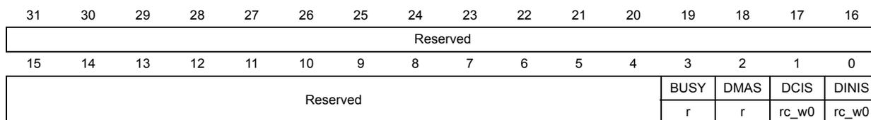
| 31 | 30 | 29 | 28 | 27 | 26 | 25 | 24 | 23 | 22 | 21 | 20 | 19 | 18 | 17 | 16 |
| Reserved | |||||||||||||||
| 15 | 14 | 13 | 12 | 11 | 10 | 9 | 8 | 7 | 6 | 5 | 4 | 3 | 2 | 1 | 0 |
| Reserved | BUSY | DMAS | DCIS | DINIS | |||||||||||
| r | r | rc_w0 | rc_w0 | ||||||||||||
Bits 31:4 Reserved, forced by hardware to 0.
Bit 3 BUSY : Busy bit
0: No block is currently being processed
1: The hash core is processing a block of data
Bit 2 DMAS : DMA Status
This bit provides information on the DMA interface activity. It is set with DMAE and cleared when DMAE=0 and no DMA transfer is ongoing. No interrupt is associated with this bit.
0: DMA interface is disabled (DMAE=0) and no transfer is ongoing
1: DMA interface is enabled (DMAE=1) or a transfer is ongoing
Bit 1 DCIS : Digest calculation completion interrupt status
This bit is set by hardware when a digest becomes ready (the whole message has been processed). It is cleared by writing it to 0 or by writing the INIT bit to 1 in the HASH_CR register.
0: No digest available in the HASH_Hx registers
1: Digest calculation complete, a digest is available in the HASH_Hx registers. An interrupt is generated if the DCIE bit is set in the HASH_IMR register.
Bit 0 DINIS : Data input interrupt status
This bit is set by hardware when the input buffer is ready to get a new block (16 locations are free). It is cleared by writing it to 0 or by writing the HASH_DIN register.
0: Less than 16 locations are free in the input buffer
1: A new block can be entered into the input buffer. An interrupt is generated if the DINIE bit is set in the HASH_IMR register.
25.4.8 HASH context swap registers (HASH_CSRx)
Address offset: 0x0F8 to 0x1C0
- • For HASH_CSR0 register: Reset value is 0x0000 0002.
- • For others registers: Reset value is 0x0000 0000 , except for STM32F43xxx devices where the HASH_CSR2 register reset value is 0x2000 0000
Additional registers are available from 0x1C1 to 0x1CC on STM32F43xxx:
- • Reset value: 0x0000 0000.
These registers contain the complete internal register states of the hash processor, and are useful when a context swap has to be done because a high-priority task has to use the hash processor while it is already in use by another task.
When such an event occurs, the HASH_CSRx registers have to be read and the read values have to be saved somewhere in the system memory space. Then the hash processor can be used by the preemptive task, and when hash computation is finished, the saved context can be read from memory and written back into these HASH_CSRx registers.
HASH_CSRx
Address offset: 0x0F8 to 0x1C0 on STM32F415/417xx
Address offset: 0x0F8 to 0x1CC on STM32F43xxx
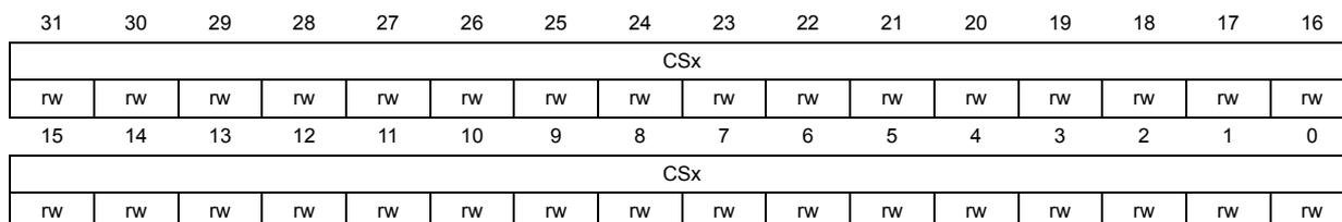
| 31 | 30 | 29 | 28 | 27 | 26 | 25 | 24 | 23 | 22 | 21 | 20 | 19 | 18 | 17 | 16 |
| CSx | |||||||||||||||
| rw | rw | rw | rw | rw | rw | rw | rw | rw | rw | rw | rw | rw | rw | rw | rw |
| 15 | 14 | 13 | 12 | 11 | 10 | 9 | 8 | 7 | 6 | 5 | 4 | 3 | 2 | 1 | 0 |
| CSx | |||||||||||||||
| rw | rw | rw | rw | rw | rw | rw | rw | rw | rw | rw | rw | rw | rw | rw | rw |
25.4.9 HASH register map
Table 9 gives the summary HASH register map and reset values.
Table 118. HASH register map and reset values on STM32F415/417xx
| Offset | Register name reset value | Register size | |||||||||||||||||||||||||||||||
|---|---|---|---|---|---|---|---|---|---|---|---|---|---|---|---|---|---|---|---|---|---|---|---|---|---|---|---|---|---|---|---|---|---|
| 31 | 30 | 29 | 28 | 27 | 26 | 25 | 24 | 23 | 22 | 21 | 20 | 19 | 18 | 17 | 16 | 15 | 14 | 13 | 12 | 11 | 10 | 9 | 8 | 7 | 6 | 5 | 4 | 3 | 2 | 1 | 0 | ||
| 0x00 | HASH_CR | Reserved | LKEY | Reserved | DINNE | NBW | ALGO[0] | MODE | DATATYPE | DMAE | INIT | Reserved | |||||||||||||||||||||
| Reset value | 0 | 0 | 0 | 0 | 0 | 0 | 0 | 0 | 0 | 0 | 0 | ||||||||||||||||||||||
| 0x04 | HASH_DIN | DATAIN | |||||||||||||||||||||||||||||||
| Reset value | 0 | 0 | 0 | 0 | 0 | 0 | 0 | 0 | 0 | 0 | 0 | 0 | 0 | 0 | 0 | 0 | 0 | 0 | 0 | 0 | 0 | 0 | 0 | 0 | 0 | 0 | 0 | 0 | 0 | 0 | 0 | 0 | |
| 0x08 | HASH_STR | Reserved | DCAL | Reserved | NBLW | ||||||||||||||||||||||||||||
| Reset value | 0 | 0 | 0 | 0 | 0 | 0 | |||||||||||||||||||||||||||
| 0x0C | HASH_HR0 | H0 | |||||||||||||||||||||||||||||||
| Reset value | 0 | 0 | 0 | 0 | 0 | 0 | 0 | 0 | 0 | 0 | 0 | 0 | 0 | 0 | 0 | 0 | 0 | 0 | 0 | 0 | 0 | 0 | 0 | 0 | 0 | 0 | 0 | 0 | 0 | 0 | 0 | 0 | |
| 0x10 | HASH_HR1 | H1 | |||||||||||||||||||||||||||||||
| Reset value | 0 | 0 | 0 | 0 | 0 | 0 | 0 | 0 | 0 | 0 | 0 | 0 | 0 | 0 | 0 | 0 | 0 | 0 | 0 | 0 | 0 | 0 | 0 | 0 | 0 | 0 | 0 | 0 | 0 | 0 | 0 | 0 | |
| 0x14 | HASH_HR2 | H2 | |||||||||||||||||||||||||||||||
| Reset value | 0 | 0 | 0 | 0 | 0 | 0 | 0 | 0 | 0 | 0 | 0 | 0 | 0 | 0 | 0 | 0 | 0 | 0 | 0 | 0 | 0 | 0 | 0 | 0 | 0 | 0 | 0 | 0 | 0 | 0 | 0 | 0 | |
| 0x18 | HASH_HR3 | H3 | |||||||||||||||||||||||||||||||
| Reset value | 0 | 0 | 0 | 0 | 0 | 0 | 0 | 0 | 0 | 0 | 0 | 0 | 0 | 0 | 0 | 0 | 0 | 0 | 0 | 0 | 0 | 0 | 0 | 0 | 0 | 0 | 0 | 0 | 0 | 0 | 0 | 0 | |
| 0x1C | HASH_HR4 | H4 | |||||||||||||||||||||||||||||||
| Reset value | 0 | 0 | 0 | 0 | 0 | 0 | 0 | 0 | 0 | 0 | 0 | 0 | 0 | 0 | 0 | 0 | 0 | 0 | 0 | 0 | 0 | 0 | 0 | 0 | 0 | 0 | 0 | 0 | 0 | 0 | 0 | 0 | |
| 0x20 | HASH_IMR | Reserved | DCIE | DINIE | |||||||||||||||||||||||||||||
| Reset value | 0 | 0 | 0 | 0 | 0 | 0 | 0 | 0 | 0 | 0 | 0 | 0 | 0 | 0 | 0 | 0 | 0 | 0 | 0 | 0 | 0 | 0 | 0 | 0 | 0 | 0 | 0 | 0 | 0 | 0 | 0 | 0 | |
| 0x24 | HASH_SR | Reserved | BUSY | DMAS | DCIS | DINIS | |||||||||||||||||||||||||||
| Reset value | 0 | 0 | 0 | 1 | |||||||||||||||||||||||||||||
| 0xF8 | HASH_CSR0 | CSR0 | |||||||||||||||||||||||||||||||
| Reset value | 0 | 0 | 0 | 0 | 0 | 0 | 0 | 0 | 0 | 0 | 0 | 0 | 0 | 0 | 0 | 0 | 0 | 0 | 0 | 0 | 0 | 0 | 0 | 0 | 0 | 0 | 0 | 0 | 0 | 0 | 1 | 0 | |
| ... | |||||||||||||||||||||||||||||||||
| ... | |||||||||||||||||||||||||||||||||
| 0x1C0 | HASH_CSR50 | CSR50 | |||||||||||||||||||||||||||||||
| Reset value | 0 | 0 | 0 | 0 | 0 | 0 | 0 | 0 | 0 | 0 | 0 | 0 | 0 | 0 | 0 | 0 | 0 | 0 | 0 | 0 | 0 | 0 | 0 | 0 | 0 | 0 | 0 | 0 | 0 | 0 | 0 | 0 | |
| Reserved | |||||||||||||||||||||||||||||||||
| 0x310 | HASH_HR0 | H0 | |||||||||||||||||||||||||||||||
| Reset value | 0 | 0 | 0 | 0 | 0 | 0 | 0 | 0 | 0 | 0 | 0 | 0 | 0 | 0 | 0 | 0 | 0 | 0 | 0 | 0 | 0 | 0 | 0 | 0 | 0 | 0 | 0 | 0 | 0 | 0 | 0 | 0 | |
| 0x314 | HASH_HR1 | H1 | |||||||||||||||||||||||||||||||
| Reset value | 0 | 0 | 0 | 0 | 0 | 0 | 0 | 0 | 0 | 0 | 0 | 0 | 0 | 0 | 0 | 0 | 0 | 0 | 0 | 0 | 0 | 0 | 0 | 0 | 0 | 0 | 0 | 0 | 0 | 0 | 0 | 0 | |
Table 118. HASH register map and reset values on STM32F415/417xx (continued)
| Offset | Register name reset value | Register size | |||||||||||||||||||||||||||||||
|---|---|---|---|---|---|---|---|---|---|---|---|---|---|---|---|---|---|---|---|---|---|---|---|---|---|---|---|---|---|---|---|---|---|
| 31 | 30 | 29 | 28 | 27 | 26 | 25 | 24 | 23 | 22 | 21 | 20 | 19 | 18 | 17 | 16 | 15 | 14 | 13 | 12 | 11 | 10 | 9 | 8 | 7 | 6 | 5 | 4 | 3 | 2 | 1 | 0 | ||
| 0x318 | HASH_HR2 | H2 | |||||||||||||||||||||||||||||||
| Reset value | 0 | 0 | 0 | 0 | 0 | 0 | 0 | 0 | 0 | 0 | 0 | 0 | 0 | 0 | 0 | 0 | 0 | 0 | 0 | 0 | 0 | 0 | 0 | 0 | 0 | 0 | 0 | 0 | 0 | 0 | 0 | 0 | |
| 0x31C | HASH_HR3 | H3 | |||||||||||||||||||||||||||||||
| Reset value | 0 | 0 | 0 | 0 | 0 | 0 | 0 | 0 | 0 | 0 | 0 | 0 | 0 | 0 | 0 | 0 | 0 | 0 | 0 | 0 | 0 | 0 | 0 | 0 | 0 | 0 | 0 | 0 | 0 | 0 | 0 | 0 | |
| 0x320 | HASH_HR4 | H4 | |||||||||||||||||||||||||||||||
| Reset value | 0 | 0 | 0 | 0 | 0 | 0 | 0 | 0 | 0 | 0 | 0 | 0 | 0 | 0 | 0 | 0 | 0 | 0 | 0 | 0 | 0 | 0 | 0 | 0 | 0 | 0 | 0 | 0 | 0 | 0 | 0 | 0 | |
Table 119. HASH register map and reset values on STM32F43xxx
| Offset | Register name reset value | Register size | |||||||||||||||||||||||||||||||
|---|---|---|---|---|---|---|---|---|---|---|---|---|---|---|---|---|---|---|---|---|---|---|---|---|---|---|---|---|---|---|---|---|---|
| 31 | 30 | 29 | 28 | 27 | 26 | 25 | 24 | 23 | 22 | 21 | 20 | 19 | 18 | 17 | 16 | 15 | 14 | 13 | 12 | 11 | 10 | 9 | 8 | 7 | 6 | 5 | 4 | 3 | 2 | 1 | 0 | ||
| 0x00 | HASH_CR | Reserved | ALGO[1] | Reserved | LKEY | Reserved | MDMAT | DINNE | NBW | ALGO[0] | MODE | DATATYPE | DMAE | INIT | Reserved | ||||||||||||||||||
| Reset value | 0 | 0 | 0 | 0 | 0 | 0 | 0 | 0 | 0 | 0 | 0 | 0 | 0 | 0 | 0 | ||||||||||||||||||
| 0x04 | HASH_DIN | DATAIN | |||||||||||||||||||||||||||||||
| Reset value | 0 | 0 | 0 | 0 | 0 | 0 | 0 | 0 | 0 | 0 | 0 | 0 | 0 | 0 | 0 | 0 | 0 | 0 | 0 | 0 | 0 | 0 | 0 | 0 | 0 | 0 | 0 | 0 | 0 | 0 | 0 | 0 | |
| 0x08 | HASH_STR | Reserved | DCAL | Reserved | NBLW | ||||||||||||||||||||||||||||
| Reset value | 0 | 0 | 0 | 0 | 0 | 0 | |||||||||||||||||||||||||||
| 0x0C | HASH_HR0 | H0 | |||||||||||||||||||||||||||||||
| Reset value | 0 | 0 | 0 | 0 | 0 | 0 | 0 | 0 | 0 | 0 | 0 | 0 | 0 | 0 | 0 | 0 | 0 | 0 | 0 | 0 | 0 | 0 | 0 | 0 | 0 | 0 | 0 | 0 | 0 | 0 | 0 | 0 | |
| 0x10 | HASH_HR1 | H1 | |||||||||||||||||||||||||||||||
| Reset value | 0 | 0 | 0 | 0 | 0 | 0 | 0 | 0 | 0 | 0 | 0 | 0 | 0 | 0 | 0 | 0 | 0 | 0 | 0 | 0 | 0 | 0 | 0 | 0 | 0 | 0 | 0 | 0 | 0 | 0 | 0 | 0 | |
| 0x14 | HASH_HR2 | H2 | |||||||||||||||||||||||||||||||
| Reset value | 0 | 0 | 0 | 0 | 0 | 0 | 0 | 0 | 0 | 0 | 0 | 0 | 0 | 0 | 0 | 0 | 0 | 0 | 0 | 0 | 0 | 0 | 0 | 0 | 0 | 0 | 0 | 0 | 0 | 0 | 0 | 0 | |
| 0x18 | HASH_HR3 | H3 | |||||||||||||||||||||||||||||||
| Reset value | 0 | 0 | 0 | 0 | 0 | 0 | 0 | 0 | 0 | 0 | 0 | 0 | 0 | 0 | 0 | 0 | 0 | 0 | 0 | 0 | 0 | 0 | 0 | 0 | 0 | 0 | 0 | 0 | 0 | 0 | 0 | 0 | |
| 0x1C | HASH_HR4 | H4 | |||||||||||||||||||||||||||||||
| Reset value | 0 | 0 | 0 | 0 | 0 | 0 | 0 | 0 | 0 | 0 | 0 | 0 | 0 | 0 | 0 | 0 | 0 | 0 | 0 | 0 | 0 | 0 | 0 | 0 | 0 | 0 | 0 | 0 | 0 | 0 | 0 | 0 | |
| 0x20 | HASH_IMR | Reserved | DCIE | DINIE | |||||||||||||||||||||||||||||
| Reset value | 0 0 0 0 0 0 0 0 0 0 0 0 0 0 0 0 0 0 0 0 0 0 0 0 0 0 0 0 0 0 | 0 | 0 | ||||||||||||||||||||||||||||||
| 0x24 | HASH_SR | Reserved | BUSY | DMAS | DCIS | DINIS | |||||||||||||||||||||||||||
| Reset value | 0 | 0 | 0 | 1 | |||||||||||||||||||||||||||||
Table 119. HASH register map and reset values on STM32F43xxx (continued)
| Offset | Register name reset value | Register size | |||||||||||||||||||||||||||||||
|---|---|---|---|---|---|---|---|---|---|---|---|---|---|---|---|---|---|---|---|---|---|---|---|---|---|---|---|---|---|---|---|---|---|
| 31 | 30 | 29 | 28 | 27 | 26 | 25 | 24 | 23 | 22 | 21 | 20 | 19 | 18 | 17 | 16 | 15 | 14 | 13 | 12 | 11 | 10 | 9 | 8 | 7 | 6 | 5 | 4 | 3 | 2 | 1 | 0 | ||
| 0xF8 | HASH_CSR0 | CSR0 | |||||||||||||||||||||||||||||||
| Reset value | 0 | 0 | 0 | 0 | 0 | 0 | 0 | 0 | 0 | 0 | 0 | 0 | 0 | 0 | 0 | 0 | 0 | 0 | 0 | 0 | 0 | 0 | 0 | 0 | 0 | 0 | 0 | 0 | 0 | 0 | 1 | 0 | |
| ... ... | |||||||||||||||||||||||||||||||||
| 0x1CC | HASH_CSR53 | CSR53 | |||||||||||||||||||||||||||||||
| Reset value | 0 | 0 | 0 | 0 | 0 | 0 | 0 | 0 | 0 | 0 | 0 | 0 | 0 | 0 | 0 | 0 | 0 | 0 | 0 | 0 | 0 | 0 | 0 | 0 | 0 | 0 | 0 | 0 | 0 | 0 | 0 | 0 | |
| Reserved | |||||||||||||||||||||||||||||||||
| 0x310 | HASH_HR0 | H0 | |||||||||||||||||||||||||||||||
| Reset value | 0 | 0 | 0 | 0 | 0 | 0 | 0 | 0 | 0 | 0 | 0 | 0 | 0 | 0 | 0 | 0 | 0 | 0 | 0 | 0 | 0 | 0 | 0 | 0 | 0 | 0 | 0 | 0 | 0 | 0 | 0 | 0 | |
| 0x314 | HASH_HR1 | H1 | |||||||||||||||||||||||||||||||
| Reset value | 0 | 0 | 0 | 0 | 0 | 0 | 0 | 0 | 0 | 0 | 0 | 0 | 0 | 0 | 0 | 0 | 0 | 0 | 0 | 0 | 0 | 0 | 0 | 0 | 0 | 0 | 0 | 0 | 0 | 0 | 0 | 0 | |
| 0x318 | HASH_HR2 | H2 | |||||||||||||||||||||||||||||||
| Reset value | 0 | 0 | 0 | 0 | 0 | 0 | 0 | 0 | 0 | 0 | 0 | 0 | 0 | 0 | 0 | 0 | 0 | 0 | 0 | 0 | 0 | 0 | 0 | 0 | 0 | 0 | 0 | 0 | 0 | 0 | 0 | 0 | |
| 0x31C | HASH_HR3 | H3 | |||||||||||||||||||||||||||||||
| Reset value | 0 | 0 | 0 | 0 | 0 | 0 | 0 | 0 | 0 | 0 | 0 | 0 | 0 | 0 | 0 | 0 | 0 | 0 | 0 | 0 | 0 | 0 | 0 | 0 | 0 | 0 | 0 | 0 | 0 | 0 | 0 | 0 | |
| 0x320 | HASH_HR4 | H4 | |||||||||||||||||||||||||||||||
| Reset value | 0 | 0 | 0 | 0 | 0 | 0 | 0 | 0 | 0 | 0 | 0 | 0 | 0 | 0 | 0 | 0 | 0 | 0 | 0 | 0 | 0 | 0 | 0 | 0 | 0 | 0 | 0 | 0 | 0 | 0 | 0 | 0 | |
| 0x324 | HASH_HR5 | H5 | |||||||||||||||||||||||||||||||
| Reset value | 0 | 0 | 0 | 0 | 0 | 0 | 0 | 0 | 0 | 0 | 0 | 0 | 0 | 0 | 0 | 0 | 0 | 0 | 0 | 0 | 0 | 0 | 0 | 0 | 0 | 0 | 0 | 0 | 0 | 0 | 0 | 0 | |
| 0x328 | HASH_HR6 | H6 | |||||||||||||||||||||||||||||||
| Reset value | 0 | 0 | 0 | 0 | 0 | 0 | 0 | 0 | 0 | 0 | 0 | 0 | 0 | 0 | 0 | 0 | 0 | 0 | 0 | 0 | 0 | 0 | 0 | 0 | 0 | 0 | 0 | 0 | 0 | 0 | 0 | 0 | |
| 0x32C | HASH_HR7 | H7 | |||||||||||||||||||||||||||||||
| Reset value | 0 | 0 | 0 | 0 | 0 | 0 | 0 | 0 | 0 | 0 | 0 | 0 | 0 | 0 | 0 | 0 | 0 | 0 | 0 | 0 | 0 | 0 | 0 | 0 | 0 | 0 | 0 | 0 | 0 | 0 | 0 | 0 | |