24. Random number generator (RNG)
This section applies to the whole STM32F4xx family, unless otherwise specified.
24.1 RNG introduction
The RNG processor is a random number generator, based on a continuous analog noise, that provides a random 32-bit value to the host when read.
The RNG passed the FIPS PUB 140-2 (2001 October 10) tests with a success ratio of 99%.
24.2 RNG main features
- • It delivers 32-bit random numbers, produced by an analog generator
- • 40 periods of the RNG_CLK clock signal between two consecutive random numbers
- • Monitoring of the RNG entropy to flag abnormal behavior (generation of stable values, or of a stable sequence of values)
- • It can be disabled to reduce power consumption
24.3 RNG functional description
Figure 232 shows the RNG block diagram.
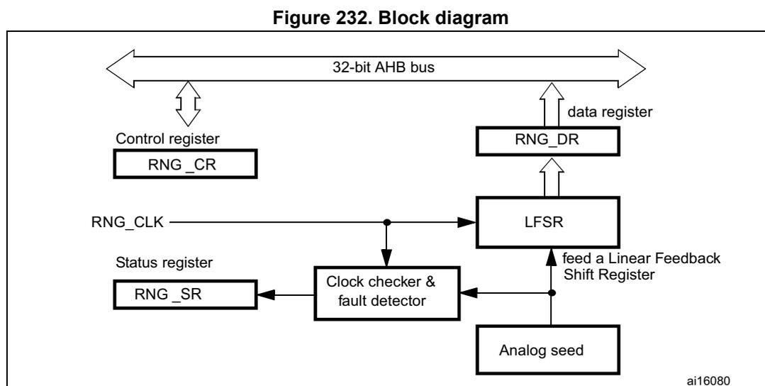
Figure 232. Block diagram
The block diagram illustrates the internal architecture of the RNG. At the top, a horizontal double-headed arrow represents the 32-bit AHB bus . Below it, the Control register (RNG_CR) and the data register (RNG_DR) are connected to this bus via vertical double-headed arrows. The RNG_DR is connected to the LFSR block below it. The LFSR block is connected to the Clock checker & fault detector block below it. The Clock checker & fault detector block is connected to the Status register (RNG_SR) block below it. The RNG_CLK input is connected to the LFSR and the Clock checker & fault detector blocks. The Analog seed block at the bottom is connected to the LFSR block, with an arrow pointing to it labeled "feed a Linear Feedback Shift Register". The identifier ai16080 is located in the bottom right corner of the diagram.
- 1. For more details about RNG Clock (RNG_CLK) source, please refer to Section 6: Reset and clock control for STM32F42xxx and STM32F43xxx (RCC) and Section 7: Reset and clock control for STM32F405xx/07xx and STM32F415xx/17xx(RCC) .
The random number generator implements an analog circuit. This circuit generates seeds that feed a linear feedback shift register (RNG_LFSR) in order to produce 32-bit random numbers.
The analog circuit is made of several ring oscillators whose outputs are XORed to generate the seeds. The RNG_LFSR is clocked by a dedicated clock (RNG_CLK) at a constant frequency, so that the quality of the random number is independent of the HCLK frequency. The contents of the RNG_LFSR are transferred into the data register (RNG_DR) when a significant number of seeds have been introduced into the RNG_LFSR.
In parallel, the analog seed and the dedicated RNG_CLK clock are monitored. Status bits (in the RNG_SR register) indicate when an abnormal sequence occurs on the seed or when the frequency of the RNG_CLK clock is too low. An interrupt can be generated when an error is detected.
24.3.1 Operation
To run the RNG, follow the steps below:
- 1. Enable the interrupt if needed (to do so, set the IE bit in the RNG_CR register). An interrupt is generated when a random number is ready or when an error occurs.
- 2. Enable the random number generation by setting the RNGEN bit in the RNG_CR register. This activates the analog part, the RNG_LFSR and the error detector.
- 3. At each interrupt, check that no error occurred (the SEIS and CEIS bits should be '0' in the RNG_SR register) and that a random number is ready (the DRDY bit is '1' in the RNG_SR register). The contents of the RNG_DR register can then be read.
As required by the FIPS PUB (Federal Information Processing Standard Publication) 140-2, the first random number generated after setting the RNGEN bit should not be used, but saved for comparison with the next generated random number. Each subsequent generated random number has to be compared with the previously generated number. The test fails if any two compared numbers are equal (continuous random number generator test).
24.3.2 Error management
If the CEIS bit is read as '1' (clock error)
In the case of a clock, the RNG is no more able to generate random numbers because the RNG_CLK clock is not correct. Check that the clock controller is correctly configured to provide the RNG clock and clear the CEIS bit. The RNG can work when the CECS bit is '0'. The clock error has no impact on the previously generated random numbers, and the RNG_DR register contents can be used.
If the SEIS bit is read as '1' (seed error)
In the case of a seed error, the generation of random numbers is interrupted for as long as the SECS bit is '1'. If a number is available in the RNG_DR register, it must not be used because it may not have enough entropy.
What you should do is clear the SEIS bit, then clear and set the RNGEN bit to reinitialize and restart the RNG.
24.4 RNG registers
The RNG is associated with a control register, a data register and a status register. They have to be accessed by words (32 bits).
24.4.1 RNG control register (RNG_CR)
Address offset: 0x00
Reset value: 0x0000 0000
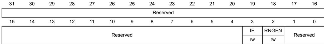
| 31 | 30 | 29 | 28 | 27 | 26 | 25 | 24 | 23 | 22 | 21 | 20 | 19 | 18 | 17 | 16 |
| Reserved | |||||||||||||||
| 15 | 14 | 13 | 12 | 11 | 10 | 9 | 8 | 7 | 6 | 5 | 4 | 3 | 2 | 1 | 0 |
| Reserved | IE | RNGEN | Reserved | ||||||||||||
| rw | rw | ||||||||||||||
Bits 31:4 Reserved, must be kept at reset value
Bit 3 IE : Interrupt enable
0: RNG Interrupt is disabled
1: RNG Interrupt is enabled. An interrupt is pending as soon as DRDY=1 or SEIS=1 or CEIS=1 in the RNG_SR register.
Bit 2 RNGEN : Random number generator enable
0: Random number generator is disabled
1: random Number Generator is enabled.
Bits 1:0 Reserved, must be kept at reset value
24.4.2 RNG status register (RNG_SR)
Address offset: 0x04
Reset value: 0x0000 0000
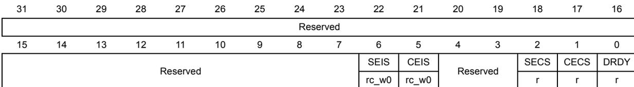
| 31 | 30 | 29 | 28 | 27 | 26 | 25 | 24 | 23 | 22 | 21 | 20 | 19 | 18 | 17 | 16 |
| Reserved | |||||||||||||||
| 15 | 14 | 13 | 12 | 11 | 10 | 9 | 8 | 7 | 6 | 5 | 4 | 3 | 2 | 1 | 0 |
| Reserved | SEIS | CEIS | Reserved | SECS | CECS | DRDY | |||||||||
| rc_w0 | rc_w0 | r | r | r | |||||||||||
Bits 31:3 Reserved, must be kept at reset value
Bit 6 SEIS : Seed error interrupt status
This bit is set at the same time as SECS, it is cleared by writing it to 0.
0: No faulty sequence detected
1: One of the following faulty sequences has been detected:
- – More than 64 consecutive bits at the same value (0 or 1)
- – More than 32 consecutive alternances of 0 and 1 (0101010101...01)
An interrupt is pending if IE = 1 in the RNG_CR register.
Bit 5 CEIS : Clock error interrupt status
This bit is set at the same time as CECS, it is cleared by writing it to 0.
0: The RNG_CLK clock was correctly detected
1: The RNG_CLK was not correctly detected ( \( f_{RNG\_CLK} < f_{HCLK}/16 \) )
An interrupt is pending if IE = 1 in the RNG_CR register.
Bits 4:3 Reserved, must be kept at reset value
Bit 2 SECS : Seed error current status0: No faulty sequence has currently been detected. If the SEIS bit is set, this means that a faulty sequence was detected and the situation has been recovered.
1: One of the following faulty sequences has been detected:
- – More than 64 consecutive bits at the same value (0 or 1)
- – More than 32 consecutive alternances of 0 and 1 (0101010101...01)
0: The RNG_CLK clock has been correctly detected. If the CEIS bit is set, this means that a clock error was detected and the situation has been recovered
1: The RNG_CLK was not correctly detected ( \( f_{\text{RNG\_CLK}} < f_{\text{HCLK}}/16 \) ).
Bit 0 DRDY : Data ready0: The RNG_DR register is not yet valid, no random data is available
1: The RNG_DR register contains valid random data
Note: An interrupt is pending if IE = 1 in the RNG_CR register.
Once the RNG_DR register has been read, this bit returns to 0 until a new valid value is computed.
24.4.3 RNG data register (RNG_DR)
Address offset: 0x08
Reset value: 0x0000 0000
The RNG_DR register is a read-only register that delivers a 32-bit random value when read. After being read, this register delivers a new random value after a maximum time of 40 periods of the RNG_CLK clock. The software must check that the DRDY bit is set before reading the RNDATA value.
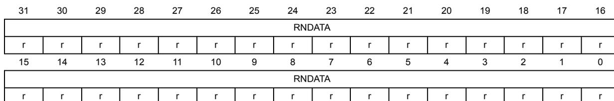
| 31 | 30 | 29 | 28 | 27 | 26 | 25 | 24 | 23 | 22 | 21 | 20 | 19 | 18 | 17 | 16 |
| RNDATA | |||||||||||||||
| r | r | r | r | r | r | r | r | r | r | r | r | r | r | r | r |
| 15 | 14 | 13 | 12 | 11 | 10 | 9 | 8 | 7 | 6 | 5 | 4 | 3 | 2 | 1 | 0 |
| RNDATA | |||||||||||||||
| r | r | r | r | r | r | r | r | r | r | r | r | r | r | r | r |
Bits 31:0
RNDATA
: Random data
32-bit random data.
24.4.4 RNG register map
Table 117 gives the RNG register map and reset values.
Table 117. RNG register map and reset map
| Offset | Register name reset value | Register size | ||||||||||||||||||||||||||||||
|---|---|---|---|---|---|---|---|---|---|---|---|---|---|---|---|---|---|---|---|---|---|---|---|---|---|---|---|---|---|---|---|---|
| 31 | 30 | 29 | 28 | 27 | 26 | 25 | 24 | 23 | 22 | 21 | 20 | 19 | 18 | 17 | 16 | 15 | 14 | 13 | 12 | 11 | 10 | 9 | 8 | 7 | 6 | 5 | 4 | 3 | 2 | 1 | 0 | |
| 0x00 | RNG_CR 0x00000000 | Reserved | IE | RNGEN | Reserved | |||||||||||||||||||||||||||
| 0x04 | RNG_SR 0x00000000 | Reserved | SEIS | CEIS | Reserved | SECS | CECS | DRDY | ||||||||||||||||||||||||
| 0x08 | RNG_DR 0x00000000 | RNDATA[31:0] | ||||||||||||||||||||||||||||||