23. Cryptographic processor (CRYP)
This section applies to STM32F415/417xx and STM32F43xxx devices.
23.1 CRYP introduction
The cryptographic processor can be used to both encipher and decipher data using the DES, Triple-DES or AES (128, 192, or 256) algorithms. It is a fully compliant implementation of the following standards:
- • The data encryption standard (DES) and Triple-DES (TDES) as defined by Federal Information Processing Standards Publication (FIPS PUB 46-3, 1999 October 25). It follows the American National Standards Institute (ANSI) X9.52 standard.
- • The advanced encryption standard (AES) as defined by Federal Information Processing Standards Publication (FIPS PUB 197, 2001 November 26)
The CRYP processor performs data encryption and decryption using DES and TDES algorithms in Electronic codebook (ECB) or Cipher block chaining (CBC) mode.
The CRYP peripheral is a 32-bit AHB2 peripheral. It supports DMA transfer for incoming and processed data, and has input and output FIFOs (each 8 words deep).
23.2 CRYP main features
- • Suitable for AES, DES and TDES enciphering and deciphering operations
- • AES
- – Supports the ECB, CBC, CTR, CCM and GCM chaining algorithms (CCM and GCM are available on STM32F42xxx and STM32F43xxx only)
- – Supports 128-, 192- and 256-bit keys
- – 4 × 32-bit initialization vectors (IV) used in the CBC, CTR, CCM and GCM modes
Table 112. Number of cycles required to process each 128-bit block (STM32F415/417xx)
| Algorithm / Key size | ECB | CBC | CTR |
|---|---|---|---|
| 128b | 14 | 14 | 14 |
| 192b | 16 | 16 | 16 |
| 256b | 18 | 18 | 18 |
Table 113. Number of cycles required to process each 128-bit block (STM32F43xxx)
| Algorithm / Key size | ECB | CBC | CTR | GCM | CCM | ||||||
|---|---|---|---|---|---|---|---|---|---|---|---|
| Init | Header | Payload | Tag | Init | Header | Payload | Tag | ||||
| 128b | 14 | 14 | 14 | 24 | 10 | 14 | 14 | 12 | 14 | 25 | 14 |
Table 113. Number of cycles required to process each 128-bit block (STM32F43xxx)
| 192b | 16 | 16 | 16 | 28 | 10 | 16 | 16 | 14 | 16 | 29 | 16 |
| 256b | 18 | 18 | 18 | 32 | 10 | 18 | 18 | 16 | 18 | 33 | 18 |
- • DES/TDES
- – Direct implementation of simple DES algorithms (a single key, K1, is used)
- – Supports the ECB and CBC chaining algorithms
- – Supports 64-, 128- and 192-bit keys (including parity)
- – 2 × 32-bit initialization vectors (IV) used in the CBC mode
- – 16 HCLK cycles to process one 64-bit block in DES
- – 48 HCLK cycles to process one 64-bit block in TDES
- • Common to DES/TDES and AES
- – IN and OUT FIFO (each with an 8-word depth, a 32-bit width, corresponding to 4 DES blocks or 2 AES blocks)
- – Automatic data flow control with support of direct memory access (DMA) (using 2 channels, one for incoming data the other for processed data)
- – Data swapping logic to support 1-, 8-, 16- or 32-bit data
23.3 CRYP functional description
The cryptographic processor implements a Triple-DES (TDES, that also supports DES) core and an AES cryptographic core. Section 23.3.1 and Section 23.3.2 provide details on these cores.
Since the TDES and the AES algorithms use block ciphers, incomplete input data blocks have to be padded prior to encryption (extra bits should be appended to the trailing end of the data string). After decryption, the padding has to be discarded. The hardware does not manage the padding operation, the software has to handle it.
Figure 216 shows the block diagram of the cryptographic processor.
Figure 216. Block diagram (STM32F415/417xx)
The block diagram illustrates the internal architecture of the cryptographic processor. At the top, a horizontal double-headed arrow represents the 32-bit AHB2 bus . Below the bus, on the left, is a vertical stack of registers: CRYP_SR (Status), CRYP_DMACR (DMA control register), CRYP_IMSCR (Interrupt register), CRYP_RIS (Interrupt register), CRYP_MISR (Interrupt register), and CRYP_CR (Control register). These registers are connected to the bus via a vertical double-headed arrow. In the center, the CRYP_DIN block contains an 8 × 32-bit IN FIFO , which receives data from the bus and sends it to a swapping block. Below the swapping block is the DES/TDES/AES Processor core . On the right, the CRYP_DOUT block contains an 8 × 32-bit OUT FIFO , which receives data from the processor core through another swapping block and sends it back to the bus. At the bottom left, two more registers, CRYP_IV0...IV1 (Initialization vectors) and CRYP_K0...K3 (Key), are connected to the processor core. The IVs are labeled IV0...IV127 and the Key is labeled k255...k0 . The diagram is labeled ai16068b in the bottom right corner.
Figure 217. Block diagram (STM32F43xxx)
The diagram illustrates the internal architecture of the CRYP block. At the top, a horizontal double-headed arrow represents the 32-bit AHB2 bus . Below this bus, several components are connected:
- Status : A block containing the CRYP_SR register, connected to the bus via a double-headed arrow.
- DMA control register : Contains the CRYP_DMACR register, connected to the bus via a double-headed arrow.
- Interrupt registers : A block containing CRYP_IMSCR , CRYP_RIS , and CRYP_MISR registers, connected to the bus via a double-headed arrow.
- Control register : Contains the CRYP_CR register, connected to the bus via a double-headed arrow.
- CRYP_DIN : An input data register connected to the bus via a double-headed arrow. It contains an 8 × 32-bit IN FIFO . Below the FIFO is a swapping block.
- CRYP_DOUT : An output data register connected to the bus via a double-headed arrow. It contains an 8 × 32-bit OUT FIFO . Below the FIFO is a swapping block.
- Initialization vectors : A block containing CRYP_IV0...IV1 (labeled IV0...IV127 ), connected to the DES/TDES/AES Processor core .
- Key : A block containing CRYP_K0...K3 (labeled k255...k0 ), connected to the DES/TDES/AES Processor core .
- Context swapping : A block containing CRYP_CSGCMCCM0..7 and CRYP_CSGCM0..7 registers, connected to the DES/TDES/AES Processor core .
- DES/TDES/AES Processor core : The central processing unit, which receives data from the swapping blocks and registers, and sends data back to them.
MS30441V1
23.3.1 DES/TDES cryptographic core
The DES/Triple-DES cryptographic core consists of three components:
- • The DES algorithm (DEA)
- • Multiple keys (1 for the DES algorithm, 1 to 3 for the TDES algorithm)
- • The initialization vector (used in the CBC mode)
The basic processing involved in the TDES is as follows: an input block is read in the DEA and encrypted using the first key, K1 (K0 is not used in TDES mode). The output is then decrypted using the second key, K2, and encrypted using the third key, K3. The key depends on the algorithm which is used:
- • DES mode: Key = [K1]
- • TDES mode: Key = [K3 K2 K1]
where \( Kx = [KxR \ KxL] \) , R = right, L = left
According to the mode implemented, the resultant output block is used to calculate the ciphertext.
Note that the outputs of the intermediate DEA stages is never revealed outside the cryptographic boundary.
The TDES allows three different keying options:
- • Three independent keys
The first option specifies that all the keys are independent, that is, K1, K2 and K3 are independent. FIPS PUB 46-3 – 1999 (and ANSI X9.52 – 1998) refers to this option as the Keying Option 1 and, to the TDES as 3-key TDES.
- • Two independent keys
The second option specifies that K1 and K2 are independent and K3 is equal to K1, that is, K1 and K2 are independent, K3 = K1. FIPS PUB 46-3 – 1999 (and ANSI X9.52 – 1998) refers to this second option as the Keying Option 2 and, to the TDES as 2-key TDES.
- • Three equal keys
The third option specifies that K1, K2 and K3 are equal, that is, K1 = K2 = K3. FIPS PUB 46-3 – 1999 (and ANSI X9.52 – 1998) refers to the third option as the Keying Option 3. This “1-key” TDES is equivalent to single DES.
FIPS PUB 46-3 – 1999 (and ANSI X9.52-1998) provides a thorough explanation of the processing involved in the four operation modes supplied by the TDEA (TDES algorithm): TDES-ECB encryption, TDES-ECB decryption, TDES-CBC encryption and TDES-CBC decryption.
This reference manual only gives a brief explanation of each mode.
DES and TDES Electronic codebook (DES/TDES-ECB) mode
- • DES/TDES-ECB mode encryption
Figure 218 illustrates the encryption in DES and TDES Electronic codebook (DES/TDES-ECB) mode. A 64-bit plaintext data block (P) is used after bit/byte/half-word swapping (refer to Section 23.3.3: Data type on page 742 ) as the input block (I). The input block is processed through the DEA in the encrypt state using K1. The output of this process is fed back directly to the input of the DEA where the DES is performed in the decrypt state using K2. The output of this process is fed back directly to the input of the DEA where the DES is performed in the encrypt state using K3. The resultant 64-bit output block (O) is used, after bit/byte/half-word swapping, as ciphertext (C) and it is pushed into the OUT FIFO.
- • DES/TDES-ECB mode decryption
Figure 219 illustrates the DES/TDES-ECB decryption. A 64-bit ciphertext block (C) is used, after bit/byte/half-word swapping, as the input block (I). The keying sequence is reversed compared to that used in the encryption process. The input block is processed through the DEA in the decrypt state using K3. The output of this process is fed back directly to the input of the DEA where the DES is performed in the encrypt state using K2. The new result is directly fed to the input of the DEA where the DES is performed in the decrypt state using K1. The resultant 64-bit output block (O), after bit/byte/half-word swapping, produces the plaintext (P).
Figure 218. DES/TDES-ECB mode encryption
The diagram illustrates the encryption process. It begins with an 'IN FIFO' block containing 'plaintext P'. An arrow labeled 'P, 64 bits' points down to a 'swapping' block. A 'DATATYPE' input points to this block. The output of the 'swapping' block, also labeled 'P, 64 bits', enters a vertical stack of three 'DEA' blocks. The first 'DEA' block is labeled 'DEA, encrypt' and uses key 'K1'. The second is 'DEA, decrypt' using key 'K2'. The third is 'DEA, encrypt' using key 'K3'. Each key is shown in a box with a slash and the number '64'. The output of the third 'DEA' block is labeled 'O, 64 bits' and points down to another 'swapping' block, which also receives a 'DATATYPE' input. The output of this second 'swapping' block is labeled 'C, 64 bits' and points down to an 'OUT FIFO' block containing 'ciphertext C'. The identifier 'ai16069b' is in the bottom right corner.
1. K: key; C: cipher text; I: input block; O: output block; P: plain text.
Figure 219. DES/TDES-ECB mode decryption
The diagram illustrates the decryption process. It begins with an 'IN FIFO' block containing 'ciphertext C'. An arrow labeled 'C, 64 bits' points down to a 'swapping' block. A 'DATATYPE' input points to this block. The output of the 'swapping' block is labeled 'I, 64 bits' and enters a vertical stack of three 'DEA' blocks. The first 'DEA' block is labeled 'DEA, decrypt' and uses key 'K3'. The second is 'DEA, encrypt' using key 'K2'. The third is 'DEA, decrypt' using key 'K1'. Each key is shown in a box with a slash and the number '64'. The output of the third 'DEA' block is labeled 'O, 64 bits' and points down to another 'swapping' block, which also receives a 'DATATYPE' input. The output of this second 'swapping' block is labeled 'P, 64 bits' and points down to an 'OUT FIFO' block containing 'plaintext P'. The identifier 'MS19021V1' is in the bottom right corner.
1. K: key; C: cipher text; I: input block; O: output block; P: plain text.
DES and TDES Cipher block chaining (DES/TDES-CBC) mode
- • DES/TDES-CBC mode encryption
Figure 220 illustrates the DES and Triple-DES Cipher block chaining (DES/TDES-CBC) mode encryption. This mode begins by dividing a plaintext message into 64-bit data blocks. In TCBC encryption, the first input block ( \( I_1 \) ), obtained after bit/byte/half-word swapping (refer to Section 23.3.3: Data type on page 742 ), is formed by exclusive-ORing the first plaintext data block ( \( P_1 \) ) with a 64-bit initialization vector IV ( \( I_1 = IV \oplus P_1 \) ). The input block is processed through the DEA in the encrypt state using K1. The output of this process is fed back directly to the input of the DEA, which performs the DES in the decrypt state using K2. The output of this process is fed directly to the input of the DEA, which performs the DES in the encrypt state using K3. The resultant 64-bit output block ( \( O_1 \) ) is used directly as the ciphertext ( \( C_1 \) ), that is, \( C_1 = O_1 \) . This first ciphertext block is then exclusive-ORed with the second plaintext data block to produce the second input block, \( (I_2) = (C_1 \oplus P_2) \) . Note that \( I_2 \) and \( P_2 \) now refer to the second block. The second input block is processed through the TDEA to produce the second ciphertext block. This encryption process continues to “chain” successive cipher and plaintext blocks together until the last plaintext block in the message is encrypted. If the message does not consist of an integral number of data blocks, then the final partial data block should be encrypted in a manner specified for the application.
- • DES/TDES-CBC mode decryption
In DES/TDES-CBC decryption (see Figure 221 ), the first ciphertext block ( \( C_1 \) ) is used directly as the input block ( \( I_1 \) ). The keying sequence is reversed compared to that used for the encrypt process. The input block is processed through the DEA in the decrypt state using K3. The output of this process is fed directly to the input of the DEA where the DES is processed in the encrypt state using K2. This resulting value is directly fed to the input of the DEA where the DES is processed in the decrypt state using K1. The resulting output block is exclusive-ORed with the IV (which must be the same as that used during encryption) to produce the first plaintext block ( \( P_1 = O_1 \oplus IV \) ). The second ciphertext block is then used as the next input block and is processed through the TDEA. The resulting output block is exclusive-ORed with the first ciphertext block to produce the second plaintext data block ( \( P_2 = O_2 \oplus C_1 \) ). (Note that \( P_2 \) and \( O_2 \) refer to the second block of data.) The TCBC decryption process continues in this manner until the last complete ciphertext block has been decrypted. Ciphertext representing a partial data block must be decrypted in a manner specified for the application.
Figure 220. DES/TDES-CBC mode encryption
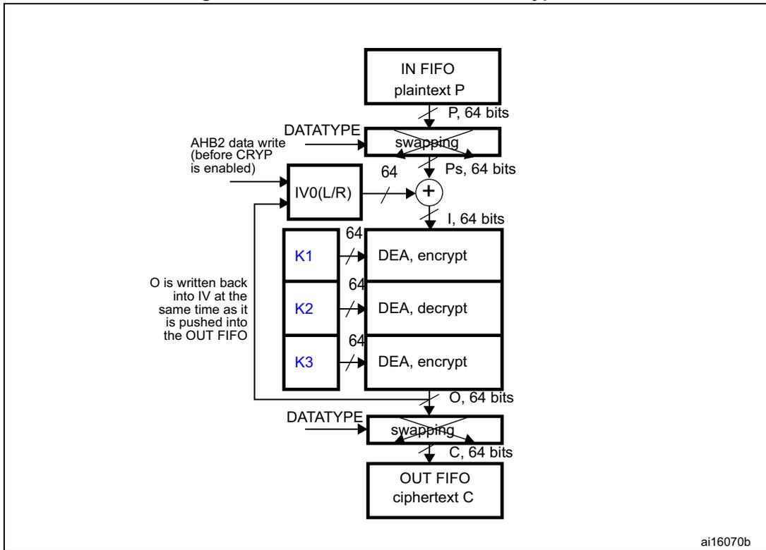
The diagram illustrates the data flow for DES/TDES-CBC mode encryption. It starts with an IN FIFO containing plaintext P . A 64-bit block P is read from the FIFO and passes through a swapping block controlled by DATATYPE . The output is Ps, 64 bits . This block is then XORed ( + ) with the output of IV0(L/R) . The result is I, 64 bits . This input block I is processed by three DEA (Data Encryption Algorithm) blocks in sequence: DEA, encrypt with key K1 , DEA, decrypt with key K2 , and DEA, encrypt with key K3 . The output of the third DEA block is O, 64 bits . This block O is written back into the IV0(L/R) register at the same time as it is pushed into the OUT FIFO as ciphertext C . Before being pushed into the OUT FIFO , the block O passes through another swapping block controlled by DATATYPE . The final output is C, 64 bits .
ai16070b
- 1. K: key; C: cipher text; I: input block; O: output block; Ps: plain text before swapping (when decoding) or after swapping (when encoding); P: plain text; IV: initialization vectors.
Figure 221. DES/TDES-CBC mode decryption
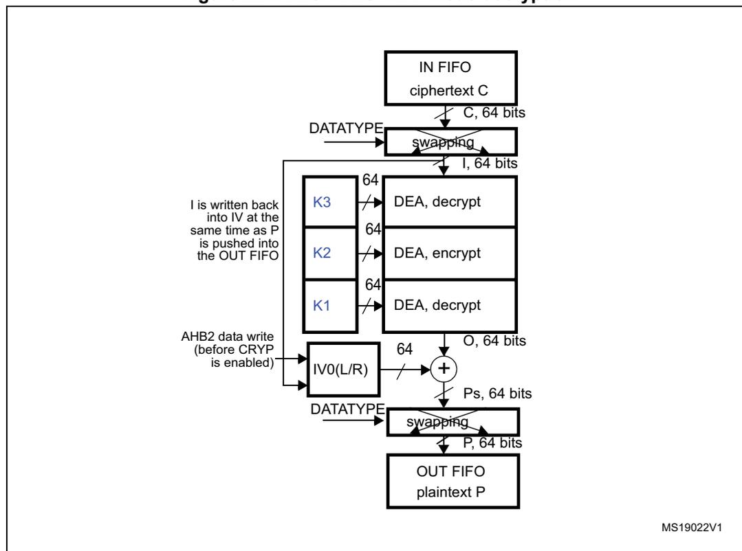
- 1. K: key; C: cipher text; I: input block; O: output block; Ps: plain text before swapping (when decoding) or after swapping (when encoding); P: plain text; IV: initialization vectors.
23.3.2 AES cryptographic core
The AES cryptographic core consists of three components:
- • The AES algorithm (AEA: advanced encryption algorithm)
- • Multiple keys
- • Initialization vector(s) or Nonce
The AES utilizes keys of 3 possible lengths: 128, 192 or 256 bits and, depending on the operation mode used, zero or one 128-bit initialization vector (IV).
The basic processing involved in the AES is as follows: an input block of 128 bits is read from the input FIFO and sent to the AEA to be encrypted using the key (K0...3). The key format depends on the key size:
- • If Key size = 128: Key = [K3 K2]
- • If Key size = 192: Key = [K3 K2 K1]
- • If Key size = 256: Key = [K3 K2 K1 K0]
where \( K_x = [K_{xR} K_{xL}] \) , R=right, L=left
According to the mode implemented, the resultant output block is used to calculate the ciphertext.
FIPS PUB 197 (November 26, 2001) provides a thorough explanation of the processing involved in the four operation modes supplied by the AES core: AES-ECB encryption, AES-
ECB decryption, AES-CBC encryption and AES-CBC decryption. This reference manual only gives a brief explanation of each mode.
AES Electronic codebook (AES-ECB) mode
- • AES-ECB mode encryption
Figure 222 illustrates the AES Electronic codebook (AES-ECB) mode encryption.
In AES-ECB encryption, a 128-bit plaintext data block (P) is used after bit/byte/half-word swapping (refer to Section 23.3.3: Data type on page 742 ) as the input block (I). The input block is processed through the AEA in the encrypt state using the 128, 192 or 256-bit key. The resultant 128-bit output block (O) is used after bit/byte/half-word swapping as ciphertext (C). It is then pushed into the OUT FIFO.
- • AES-ECB mode decryption
Figure 223 illustrates the AES Electronic codebook (AES-ECB) mode encryption.
To perform an AES decryption in the ECB mode, the secret key has to be prepared (it is necessary to execute the complete key schedule for encryption) by collecting the last round key, and using it as the first round key for the decryption of the ciphertext. This preparation function is computed by the AES core. Refer to Section 23.3.6: Procedure to perform an encryption or a decryption for more details on how to prepare the key.
In AES-ECB decryption, a 128-bit ciphertext block (C) is used after bit/byte/half-word swapping as the input block (I). The keying sequence is reversed compared to that of the encryption process. The resultant 128-bit output block (O), after bit/byte or half-word swapping, produces the plaintext (P).
Figure 222. AES-ECB mode encryption
graph TD
    IN_FIFO["IN FIFO
plaintext P"] -- "P, 128 bits" --> SWAP1["swapping
DATATYPE"]
    SWAP1 -- "I, 128 bits" --> AEA["AEA, encrypt
K0...3(1)
128/192 or 256"]
    AEA --> SWAP2["swapping
DATATYPE"]
    SWAP2 -- "C, 128 bits" --> OUT_FIFO["OUT FIFO
ciphertext C"]
- 1. K: key; C: cipher text; I: input block; O: output block; P: plain text.
- 2. If Key size = 128: Key = [K3 K2].
If Key size = 192: Key = [K3 K2 K1]
If Key size = 256: Key = [K3 K2 K1 K0].
Figure 223. AES-ECB mode decryption
- 1. K: key; C: cipher text; I: input block; O: output block; P: plain text.
- 2. If Key size = 128 => Key = [K3 K2].
If Key size = 192 => Key = [K3 K2 K1]
If Key size = 256 => Key = [K3 K2 K1 K0].
AES Cipher block chaining (AES-CBC) mode
- • AES-CBC mode encryption
The AES Cipher block chaining (AES-CBC) mode decryption is shown on Figure 224 .
In AES-CBC encryption, the first input block ( \( I_1 \) ) obtained after bit/byte/half-word swapping (refer to Section 23.3.3: Data type on page 742 ) is formed by exclusive-ORing the first plaintext data block ( \( P_1 \) ) with a 128-bit initialization vector IV ( \( I_1 = IV \oplus P_1 \) ). The input block is processed through the AEA in the encrypt state using the 128-, 192- or 256-bit key ( \( K_0 \dots K_3 \) ). The resultant 128-bit output block ( \( O_1 \) ) is used directly as ciphertext ( \( C_1 \) ), that is, \( C_1 = O_1 \) . This first ciphertext block is then exclusive-ORed with the second plaintext data block to produce the second input block, \( (I_2) = (C_1 \oplus P_2) \) . Note that \( I_2 \) and \( P_2 \) now refer to the second block. The second input block is processed through the AEA to produce the second ciphertext block. This encryption process continues to “chain” successive cipher and plaintext blocks together until the last plaintext block in the message is encrypted. If the message does not consist of an integral number of data blocks, then the final partial data block should be encrypted in a manner specified for the application.
In the CBC mode, like in the ECB mode, the secret key must be prepared to perform an AES decryption. Refer to Section 23.3.6: Procedure to perform an encryption or a decryption on page 747 for more details on how to prepare the key.
- • AES-CBC mode decryption
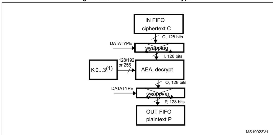
In AES-CBC decryption (see Figure 225 ), the first 128-bit ciphertext block ( \( C_1 \) ) is used directly as the input block ( \( I_1 \) ). The input block is processed through the AEA in the decrypt state using the 128-, 192- or 256-bit key. The resulting output block is exclusive-ORed with the 128-bit initialization vector IV (which must be the same as that used during encryption) to produce the first plaintext block ( \( P_1 = O_1 \oplus IV \) ). The second ciphertext block is then used as the next input block and is processed through the AEA. The resulting output block is exclusive-ORed with the first ciphertext block to produce the second plaintext data block ( \( P_2 = O_2 \oplus C_1 \) ). (Note that \( P_2 \) and \( O_2 \) refer to the second
block of data.) The AES-CBC decryption process continues in this manner until the last complete ciphertext block has been decrypted. Ciphertext representing a partial data block must be decrypted in a manner specified for the application.
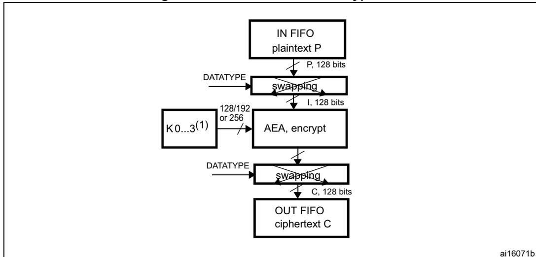
Figure 224. AES-CBC mode encryption
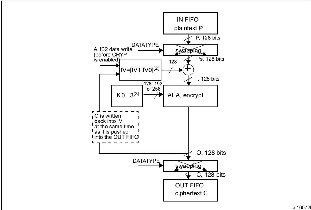
The diagram illustrates the AES-CBC mode encryption process. The data flow is as follows:
- IN FIFO (plaintext P) provides a 128-bit block ( P, 128 bits ).
- The block enters a swapping unit controlled by DATATYPE .
- The swapped plaintext Ps, 128 bits is XORed (indicated by a + in a circle) with the Initialization Vector IV=[IV1 IV0] (2) .
- The result I, 128 bits enters the AEA, encrypt block.
- The encryption block uses a key K0...3 (3) of size 128, 192, or 256 bits.
- The output O, 128 bits is fed back to the IV register (indicated by a dashed box stating: "O is written back into IV at the same time as it is pushed into the OUT FIFO").
- The output O also passes through another swapping unit controlled by DATATYPE .
- The final ciphertext C ( C, 128 bits ) is stored in the OUT FIFO .
- An external input AHB2 data write (before CRYP is enabled) is shown providing the initial IV and Key values.
- 1. K: key; C: cipher text; I: input block; O: output block; Ps: plain text before swapping (when decoding) or after swapping (when encoding); P: plain text; IV: Initialization vectors.
- 2. \( IVx = [IVxR \ IVxL] \) , R=right, L=left.
- 3. If Key size = 128 => Key =
\(
[K3 \ K2]
\)
.
If Key size = 192 => Key = \( [K3 \ K2 \ K1] \)
If Key size = 256 => Key = \( [K3 \ K2 \ K1 \ K0] \) .
Figure 225. AES-CBC mode decryption
' block (128 bits). The 'IV' block is updated by an 'AHB2 data write (before CRYP is enabled)'. The XOR result is 'Ps, 128 bits', which then enters another 'swapping' block. The output of this second 'swapping' block is 'P, 128 bits', which is then pushed into the 'OUT FIFO plaintext P'. A dashed box indicates that 'I is written back into IV at the same time I as P is pushed into the OUT FIFO'. A note 'MS19024V1' is in the bottom right corner.](/RM0090-STM32F405-415-407-417-427-437-429-439/4404b46dac18960c034d364f9153b49a_img.jpg)
- 1. K: key; C: cipher text; I: input block; O: output block; Ps: plain text before swapping (when decoding) or after swapping (when encoding); P: plain text; IV: Initialization vectors.
- 2. \( IV_x = [IV_{xR} \ IV_{xL}] \) , R=right, L=left.
- 3. If Key size = 128 => Key = [K3 K2].
If Key size = 192 => Key = [K3 K2 K1].
If Key size = 256 => Key = [K3 K2 K1 K0].
AES counter mode (AES-CTR) mode
The AES counter mode uses the AES block as a key stream generator. The generated keys are then XORed with the plaintext to obtain the cipher. For this reason, it makes no sense to speak of different CTR encryption/decryption, since the two operations are exactly the same.
In fact, given:
- • Plaintext: \( P[0], P[1], \dots, P[n] \) (128 bits each)
- • A key K to be used (the size does not matter)
- • An initial counter block (call it ICB but it has the same functionality as the IV of CBC)
The cipher is computed as follows:
\( C[i] = \text{enc}(\text{iv}[i]) \oplus P[i] \) , where:
\( \text{iv}[0] = \text{ICB} \) and \( \text{iv}[i+1] = \text{func}(\text{iv}[i]) \) , where func is an update function applied to the previous iv block; func is basically an increment of one of the fields composing the iv block.
Given that the ICB for decryption is the same as the one for encryption, the key stream generated during decryption is the same as the one generated during encryption. Then, the ciphertext is XORed with the key stream in order to retrieve the original plaintext. The decryption operation therefore acts exactly in the same way as the encryption operation.
Figure 226 and Figure 227 illustrate AES-CTR encryption and decryption, respectively.
Figure 226. AES-CTR mode encryption
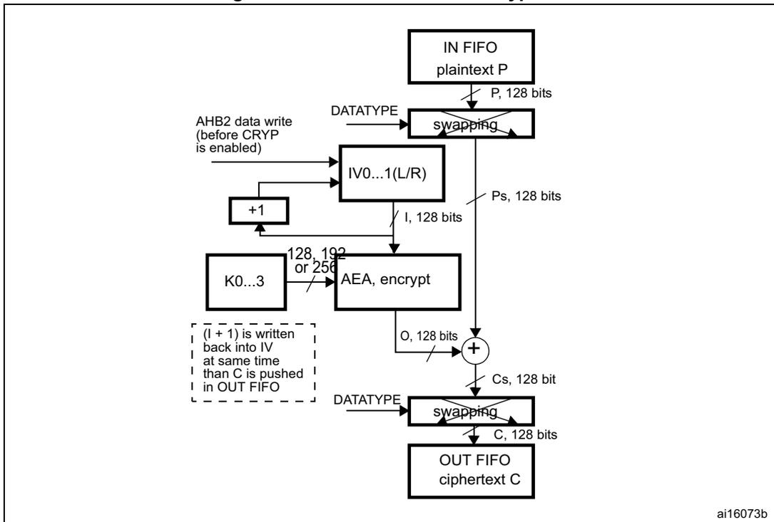
The diagram illustrates the data flow for AES-CTR mode encryption. It starts with an 'IN FIFO' block labeled 'plaintext P'. An arrow labeled 'P, 128 bits' points down to a 'swapping' block. A 'DATATYPE' control signal is also input to this block. The output of the 'swapping' block is labeled 'Ps, 128 bits' and points down to an XOR gate (represented by a circle with a '+'). The XOR gate also receives an input from an 'AEA, encrypt' block, labeled 'O, 128 bits'. The output of the XOR gate is labeled 'Cs, 128 bit' and points down to another 'swapping' block. A 'DATATYPE' control signal is input to this block. The output of this 'swapping' block is labeled 'C, 128 bits' and points down to an 'OUT FIFO' block labeled 'ciphertext C'. The 'AEA, encrypt' block receives two inputs: 'K0...3' (labeled '128, 192 or 256') and 'I, 128 bits'. The 'I, 128 bits' input comes from an 'IV0...1(L/R)' block. The 'IV0...1(L/R)' block receives an input from an 'AHB2 data write (before CRYP is enabled)' and an input from a '+1' block. The '+1' block receives an input from the 'I, 128 bits' line. A dashed box contains the text: '(I + 1) is written back into IV at same time than C is pushed in OUT FIFO'.
- 1. K: key; C: cipher text; I: input Block; o: output block; Ps: plain text before swapping (when decoding) or after swapping (when encoding); Cs: cipher text after swapping (when decoding) or before swapping (when encoding); P: plain text; IV: Initialization vectors.
Figure 227. AES-CTR mode decryption

- 1. K: key; C: cipher text; I: input Block; o: output block; Ps: plain text before swapping (when decoding) or after swapping (when encoding); Cs: cipher text after swapping (when decoding) or before swapping (when encoding); P: plain text; IV: Initialization vectors.
Figure 228 shows the structure of the IV block as defined by the standard [2]. It is composed of three distinct fields.
Figure 228. Initial counter block structure for the Counter mode
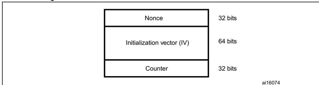
- • Nonce is a 32-bit, single-use value. A new nonce should be assigned to each different communication.
- • The initialization vector (IV) is a 64-bit value and the standard specifies that the encryptor must choose IV so as to ensure that a given value is used only once for a given key
- • The counter is a 32-bit big-endian integer that is incremented each time a block has been encrypted. The initial value of the counter should be set to '1'.
The block increments the least significant 32 bits, while it leaves the other (most significant) 96 bits unchanged.
AES Galois/counter mode (GCM)
The AES Galois/counter mode (GCM) allows encrypting and authenticating the plaintext, and generating the correspondent ciphertext and tag (also known as message authentication code or message integrity check). This algorithm is based on AES counter mode to ensure confidentiality. It uses a multiplier over a fixed finite field to generate the tag. An initialization vector is required at the beginning of the algorithm.
The message to be processed is split into 2 parts:
- • The header (also known as additional authentication data): data which is authenticated but not protected (such as information for routing the packet)
- • The payload (also known as plaintext or ciphertext): the message itself which is authenticated and encrypted.
Note: The header must precede the payload and the two parts cannot be mixed together.
The GCM standard requires to pass, at the end of the message, a specific 128-bit block composed of the size of the header (64 bits) and the size of the payload (64 bits). During the computation, the header blocks must be distinguished from the payload blocks.
In GCM mode, four steps are required to perform an encryption/decryption:
1. GCM init phase
During this first step, the HASH key is calculated and saved internally to be used for processing all the blocks. It is recommended to follow the sequence below:
- Make sure that the cryptographic processor is disabled by clearing the CRYPTEN bit in the CRYP_CR register.
- Select the GCM chaining mode by programming ALGOMODE bits to '01000' in CRYP_CR.
- Configure GCM_CCMPH bits to '00' in CRYP_CR to start the GCM Init phase.
- Initialize the key registers (128, 192 and 256 bits) in CRYP_KEYRx as well as the initialization vector (IV).
- Set CRYPTEN bit to '1' to start the calculation of the HASH key.
- Wait for the CRYPTEN bit to be cleared to '0' before moving on to the next phase.
- Set the CRYPTEN bit to '1'.
2. GCM header phase
This step must be performed after the GCM Init phase:
- Set the GCM_CCMPH bits to '01' in CRYP_CR to indicate that the header phase has started.
- Write the header data. Three methods can be used:
- – Program the data by blocks of 32 bits into the CRYP_DIN register, and use the IFNF flag to determine if the input FIFO can receive data. The size of the header must be a multiple of 128 bits (4 words).
- – Program the data into the CRYP_DIN register by blocks of 8 words, and use the IFEM flag to determine if the input FIFO can receive data (IFEM='1'). The size of the header must be a multiple of 128 bits (4 words).
- – Use the DMA.
- Once all header data have been supplied, wait until the BUSY bit is cleared in the CRYP_SR register.
3. GCM payload phase (encryption/decryption)
This step must be performed after the GCM header phase:
- Configure GCM_CCMPH to '10' in the CRYP_CR register.
- Select the algorithm direction (encryption or decryption) by using the ALGODIR bit in CRYP_CR.
- Program the payload message into the CRYP_DIN register, and use the IFNF flag to determine if the input FIFO can receive data. Alternatively, the data could be programmed into the CRYP_DIN register by blocks of 8 words and the IFEM flag used to determine if the input FIFO can receive data (IFEM='1'). In parallel, the
OFNE/OFFU flag of the CRYP_DOUT register can be monitored to check if the output FIFO is not empty.
- n) Repeat the previous step until all payload blocks have been encrypted or decrypted. Alternatively, DMA could be used.
- 4. GCM final phase
- This step generates the authentication tag:
- o) Configure GCM_CCMPH[1:0] to '11' in CRYP_CR.
- p) Write the input into the CRYP_DIN register 4 times. The input must contain the number of bits in the header (64 bits) concatenated with the number of bits in the payload (64 bits).
- q) Wait till the OFNE flag (FIFO output not empty) is set to '1' in the CRYP_SR register.
- r) Read the CRYP_DOUT register 4 times: the output corresponds to the authentication tag.
- s) Disable the cryptographic processor (CRYPEN bit in CRYP_CR = '0')
Note: When a decryption is performed, it is not required to compute the key at the beginning. At the end of the decryption, the generated tag should be compared with the expected tag passed with the message. In addition, the ALGODIR bit (algorithm direction) must be set to '1'. No need to disable/enable CRYP processor when moving from header phase to tag phase.
AES Galois message authentication code (GMAC)
The cryptographic processor also supports GMAC to authenticate the plaintext. It uses the GCM algorithm and a multiplier over a fixed finite field to generate the corresponding tag.
An initialization vector is required at the beginning of the algorithm.
Actually, the GMAC algorithm corresponds to the GCM algorithm applied on a message composed of the header only. As a consequence, the payload phase is not required.
AES combined cipher machine (CCM)
The CCM algorithm allows encrypting and authenticating the plaintext, as well as generating the corresponding ciphertext and tag (also known as message authentication code or message integrity check). This algorithm is based on AES counter mode to ensure confidentiality. It uses the AES CBC mode to generate a 128-bit tag.
The CCM standard (RFC 3610 Counter with CBC-MAC (CCM) dated September 2003) defines particular encoding rules for the first authentication block (called B0 in the standard). In particular, the first block includes flags, a nonce and the payload length expressed in bytes. The CCM standard specifies another format, called A or counter, for encryption/decryption. The counter is incremented during the payload phase and its 32 LSB bits are initialized to '1' during the tag generation (called A0 packet in the CCM standard).
Note: The hardware does not perform the formatting operation of the B0 packet. It should be handled by the software.
As for the GCM algorithm, the message to be processed is split into 2 parts:
- • The header (also known as additional authentication data): data which is authenticated but not protected (such as information for routing the packet)
- • The payload (also known as plaintext or ciphertext): the message itself which is authenticated and encrypted.
Note: The header part must precede the payload and the two parts cannot be mixed together.
In CCM mode, 4 steps are required to perform an encryption or decryption:
1. CCM init phase
In this first step, the B0 packet of the CCM message (1st packet) is programmed into the CRYP_DIN register. During this phase, the CRYP_DOUT register does not contain any output data.
The following sequence must be followed:
- a) Make sure that the cryptographic processor is disabled by clearing the CRYPTEN bit in the CRYP_CR register.
- b) Select the CCM chaining mode by programming the ALGOMODE bits to '01001' in the CRYP_CR register.
- c) Configure the GCM_CCMPH bits to '00' in CRYP_CR to start the CCM Init phase.
- d) Initialize the key registers (128, 192 and 256 bits) in CRYP_KEYRx as well as the initialization vector (IV).
- e) Set the CRYPTEN bit to '1' in CRYP_CR.
- f) Program the B0 packet into the input data register.
- g) Wait for the CRYPTEN bit to be cleared before moving on to the next phase.
- h) Set CRYPTEN to '1'.
2. CCM header phase
This step must be performed after the CCM Init phase. The sequence is identical for encryption and decryption.
During this phase, the CRYP_DOUT register does not contain any output data.
This phase can be skipped if there is no additional authenticated data.
The following sequence must be followed:
- i) Set the GCM_CCMPH bit to '01' in CRYP_CR to indicate that the header phase has started.
- j) Three methods can be used:
- – Program the header data by blocks of 32 bits into the CRYP_DIN register, and use the IFNF flag to determine if the input FIFO can receive data. The size of the header must be a multiple of 128 bits (4 words).
- – Program the header data into the CRYP_DIN register by blocks of 8 words, and use the IFEM flag to determine if the input FIFO can receive data (IFEM='1'). The size of the header must be a multiple of 128 bits (4 words).
- – Use the DMA.
Note: The first block B1 must be formatted with the header length. This task should be handled by software.
- k) Once all header data have been supplied, wait until the BUSY flag is cleared.
3. CCM payload phase (encryption/decryption)
This step must be performed after the CCM header phase. During this phase, the encrypted/decrypted payload is stored in the CRYP_DOUT register.
The following sequence must be followed:
- l) Configure GCM_CCMPH bits to '10' in CRYP_CR.
- m) Select the algorithm direction (encryption or decryption) by using the ALGODIR bit in CRYP_CR.
- n) Program the payload message into the CRYP_DIN register, and use the IFNF flag to determine if the input FIFO can receive data. Alternatively, the data could be programmed into the CRYP_DIN register by blocks of 8 words and the IFEM flag used to determine if the input FIFO can receive data (IFEM='1'). In parallel, the OFNE/OFFU flag of the CRYP_DOUT register can be monitored to check if the output FIFO is not empty.
- o) Repeat the previous step until all payload blocks have been encrypted or decrypted. Alternatively, DMA could be used.
- 4. CCM final phase
- This step generates the authentication tag. During this phase, the authentication tag of the message is generated and stored in the CRYP_DOUT register.
- p) Configure GCM_CCMPH[1:0] bits to '11' in CRYP_CR.
- q) Load the A0 initialized counter, and program the 128-bit A0 value by writing 4 times 32 bits into the CRYP_DIN register.
- r) Wait till the OFNE flag (FIFO output not empty) is set to '1' in the CRYP_SR register.
- s) Read the CRYP_DOUT register 4 times: the output corresponds to the encrypted authentication tag.
- t) Disable the cryptographic processor (CRYPTEN bit in CRYP_CR = '0')
Note: The hardware does not perform the formatting of the original B0 and B1 packets and the tag comparison between encryption and decryption. They have to be handled by software.
The cryptographic processor does not need to be disabled/enabled when moving from the header phase to the tag phase.
AES cipher message authentication code (CMAC)
The CMAC algorithm allows authenticating the plaintext, and generating the corresponding tag. The CMAC sequence is identical to the CCM one, except that the payload phase is skipped.
23.3.3 Data type
Data enter the CRYP processor 32 bits (word) at a time as they are written into the CRYP_DIN register. The principle of the DES is that streams of data are processed 64 bits by 64 bits and, for each 64-bit block, the bits are numbered from M1 to M64, with M1 the left-most bit and M64 the right-most bit of the block. The same principle is used for the AES, but with a 128-bit block size.
The system memory organization is little-endian: whatever the data type (bit, byte, 16-bit half-word, 32-bit word) used, the least-significant data occupy the lowest address locations. A bit, byte, or half-word swapping operation (depending on the kind of data to be encrypted) therefore has to be performed on the data read from the IN FIFO before they enter the CRYP processor. The same swapping operation should be performed on the CRYP data before they are written into the OUT FIFO. For example, the operation would be byte swapping for an ASCII text stream.
The kind of data to be processed is configured with the DATATYPE bitfield in the CRYP control register (CRYP_CR).
Table 114. Data types
| DATATYPE in CRYP_CR | Swapping performed | System memory data (plaintext or cypher) |
|---|---|---|
| 00b | No swapping | Example: TDES block value 0xABCD77206973FE01 is represented in system memory as: TDES block size = 64bit = 2x 32 bit Image: Diagram for 00b: A 64-bit block 0xABCD77206973FE01 is shown. An arrow points to system memory where the value 0xABCD7720 is at address @ and 0x6973FE01 is at address @+4. system memory 0xABCD7720 @ 0x6973FE01 @+4 |
| 01b | Half-word (16-bit) swapping | Example: TDES block value 0xABCD77206973FE01 is represented in system memory as: TDES block size = 64bit = 2x 32 bit Image: Diagram for 01b: A 64-bit block 0xABCD77206973FE01 is shown. An arrow points to system memory where the value 0x7720ABCD is at address @ and 0xFE016973 is at address @+4. system memory 0x7720ABCD @ 0xFE016973 @+4 |
| 10b | Byte (8-bit) swapping | Example: TDES block value 0xABCD77206973FE01 is represented in system memory as: TDES block size = 64bit = 2x 32 bit Image: Diagram for 10b: A 64-bit block 0xABCD77206973FE01 is shown. An arrow points to system memory where the value 0x2077CDAB is at address @ and 0x01FE7369 is at address @+4. system memory 0x2077CDAB @ 0x01FE7369 @+4 |
| 11b | Bit swapping | TDES block value 0x4E6F772069732074 is represented in system memory as: TDES Bloc size = 64bit = 2x 32 bit Image: Diagram for 11b: A 64-bit block 0x4E6F772069732074 is shown. A vertical double arrow indicates bit swapping within each 32-bit word. An arrow points to system memory where the value 0x04EEF672 is at address @ and 0x2E04CE96 is at address @+4. Below the memory addresses, the bit sequences are shown: 0100 1110 0110 1111 0110 1001 0111 0011 for the first word and 0111 0111 0010 0000 0010 0000 0111 0100 for the second word. system memory 0x04EEF672 @ 0x2E04CE96 @+4 0100 1110 0110 1111 0110 1001 0111 0011 @ 0111 0111 0010 0000 0010 0000 0111 0100 @+4 |
Figure 229 shows how the 64-bit data block M1...64 is constructed from two consecutive 32-bit words popped off the IN FIFO by the CRYP processor, according to the DATATYPE value. The same schematic can easily be extended to form the 128-bit block for the AES
cryptographic algorithm (for the AES, the block length is four 32-bit words, but swapping only takes place at word level, so it is identical to the one described here for the TDES).
Note: The same swapping is performed between the IN FIFO and the CRYP data block, and between the CRYP data block and the OUT FIFO.
Figure 229. 64-bit block construction according to DATATYPE
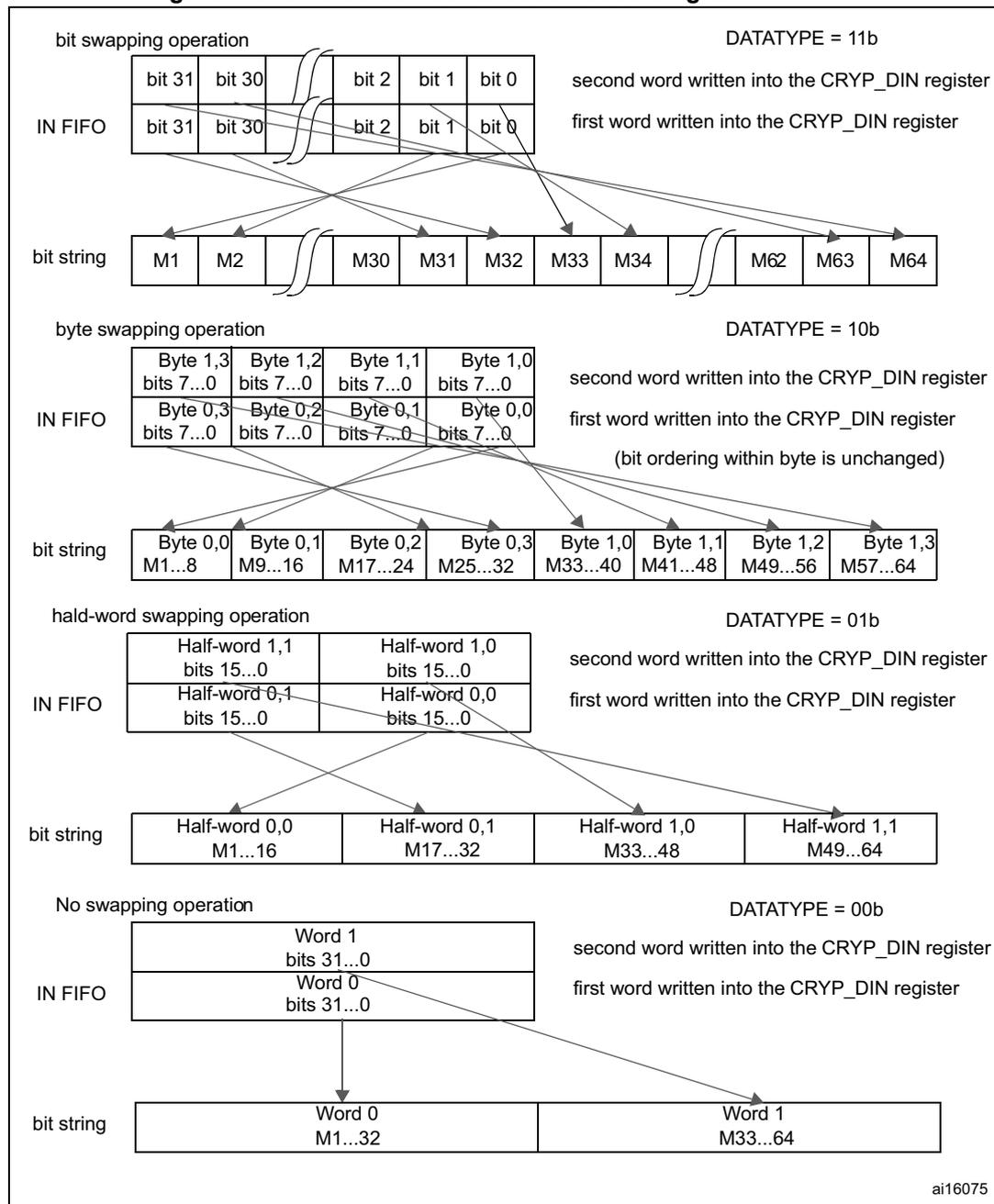
The diagram illustrates the mapping of data from the IN FIFO to the bit string for a 64-bit block, based on the DATATYPE setting. It is divided into four sections:
- bit swapping operation (DATATYPE = 11b): Shows two 32-bit words in the IN FIFO. The first word (bits 31..0) is written into the CRYP_DIN register. The bit string (M1..M64) is constructed by interleaving bits from the two words: M1..M32 come from the first word, and M33..M64 come from the second word, with bit positions swapped.
- byte swapping operation (DATATYPE = 10b): Shows two 32-bit words in the IN FIFO, each consisting of four bytes. The first word is written into the CRYP_DIN register. The bit string (M1..M64) is constructed by interleaving bytes from the two words: Byte 0,0 goes to M1..8, Byte 0,1 to M9..16, etc. The note indicates that bit ordering within a byte is unchanged.
- half-word swapping operation (DATATYPE = 01b): Shows two 32-bit words in the IN FIFO, each consisting of two half-words. The first word is written into the CRYP_DIN register. The bit string (M1..M64) is constructed by interleaving half-words from the two words: Half-word 0,0 goes to M1..16, Half-word 0,1 to M17..32, etc.
- No swapping operation (DATATYPE = 00b): Shows two 32-bit words in the IN FIFO. The first word is written into the CRYP_DIN register. The bit string (M1..M64) is constructed by concatenating the words: Word 0 goes to M1..32, and Word 1 goes to M33..64.
ai16075
23.3.4 Initialization vectors - CRYP_IV0...1(L/R)
Initialization vectors are considered as two 64-bit data items. They therefore do not have the same data format and representation in system memory as plaintext or cypher data, and they are not affected by the DATATYPE value.
Initialization vectors are defined by two consecutive 32-bit words, CRYP_IVL (left part, noted as bits IV1...32) and CRYP_IVR (right part, noted as bits IV33...64).
During the DES or TDES CBC encryption, the CRYP_IV0(L/R) bits are XORed with the 64-bit data block popped off the IN FIFO after swapping (according to the DATATYPE value), that is, with the M1...64 bits of the data block. When the output of the DEA3 block is available, it is copied back into the CRYP_IV0(L/R) vector, and this new content is XORed with the next 64-bit data block popped off the IN FIFO, and so on.
During the DES or TDES CBC decryption, the CRYP_IV0(L/R) bits are XORed with the 64-bit data block (that is, with the M1...64 bits) delivered by the TDEA1 block before swapping (according to the DATATYPE value), and pushed into the OUT FIFO. When the XORed result is swapped and pushed into the OUT FIFO, the CRYP_IV0(L/R) value is replaced by the output of the IN FIFO, then the IN FIFO is popped, and a new 64-bit data block can be processed.
During the AES CBC encryption, the CRYP_IV0...1(L/R) bits are XORed with the 128-bit data block popped off the IN FIFO after swapping (according to the DATATYPE value). When the output of the AES core is available, it is copied back into the CRYP_IV0...1(L/R) vector, and this new content is XORed with the next 128-bit data block popped off the IN FIFO, and so on.
During the AES CBC decryption, the CRYP_IV0...1(L/R) bits are XORed with the 128-bit data block delivered by the AES core before swapping (according to the DATATYPE value) and pushed into the OUT FIFO. When the XORed result is swapped and pushed into the OUT FIFO, the CRYP_IV0...1(L/R) value is replaced by the output of the IN FIFO, then the IN FIFO is popped, and a new 128-bit data block can be processed.
During the AES CTR encryption or decryption, the CRYP_IV0...1(L/R) bits are encrypted by the AES core. Then the result of the encryption is XORed with the 128-bit data block popped off the IN FIFO after swapping (according to the DATATYPE value). When the XORed result is swapped and pushed into the OUT FIFO, the counter part of the CRYP_IV0...1(L/R) value (32 LSB) is incremented.
Any write operation to the CRYP_IV0...1(L/R) registers when bit BUSY = 1b in the CRYP_SR register is disregarded (CRYP_IV0...1(L/R) register content not modified). Thus, you must check that bit BUSY = 0b before modifying initialization vectors.
Figure 230. Initialization vectors use in the TDES-CBC encryption
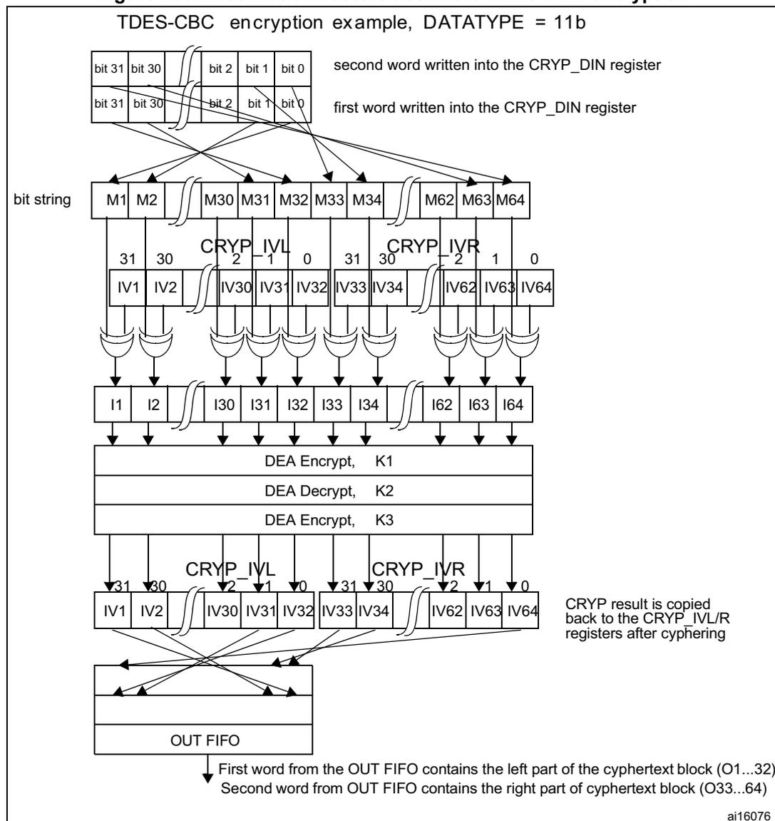
TDES-CBC encryption example, DATATYPE = 11b
The diagram illustrates the data flow for TDES-CBC encryption. At the top, two 32-bit words are shown, labeled 'second word written into the CRYP_DIN register' and 'first word written into the CRYP_DIN register'. Each word is split into two 16-bit parts: bits 31-0 and bits 15-0. These are then mapped into a 'bit string' consisting of blocks M1, M2, M30, M31, M32, M33, M34, M62, M63, and M64. Below the bit string, there are two 32-bit initialization vector registers, CRYP_IVL and CRYP_IVR. Each register is split into two 16-bit parts: bits 31-0 and bits 15-0. The bit string blocks are XORed with the corresponding IV register parts to produce intermediate values I1, I2, I30, I31, I32, I33, I34, I62, I63, and I64. These values are then processed by three DEA (Data Encryption Algorithm) blocks: 'DEA Encrypt, K1', 'DEA Decrypt, K2', and 'DEA Encrypt, K3'. The output of these blocks is then mapped back into the CRYP_IVL and CRYP_IVR registers. A note indicates that the 'CRYP result is copied back to the CRYP_IVL/R registers after cyphering'. Finally, the data is written to an 'OUT FIFO'. Two notes at the bottom explain: 'First word from the OUT FIFO contains the left part of cyphertext block (O1...32)' and 'Second word from OUT FIFO contains the right part of cyphertext block (O33..64)'. The diagram is identified by the code 'ai16076'.
23.3.5 CRYP busy state
When there is enough data in the input FIFO (at least 2 words for the DES or TDES algorithm mode, 4 words for the AES algorithm mode) and enough free-space in the output FIFO (at least 2 (DES/TDES) or 4 (AES) word locations), and when the bit CRYPTEN = 1 in the CRYP_CR register, then the cryptographic processor automatically starts an encryption or decryption process (according to the value of the ALGODIR bit in the CRYP_CR register).
This process takes 48 AHB2 clock cycles for the Triple-DES algorithm, 16 AHB2 clock cycles for the simple DES algorithm, and 14, 16 or 18 AHB2 clock cycles for the AES with key lengths of 128, 192 or 256 bits, respectively. During the whole process, the BUSY bit in the CRYP_SR register is set to '1'. At the end of the process, two (DES/TDES) or four (AES) words are written by the CRYP Core into the output FIFO, and the BUSY bit is cleared. In
the CBC, CTR mode, the initialization vectors CRYP_IVx(L/R)R (x = 0..3) are updated as well.
A write operation to the key registers (CRYP_Kx(L/R)R, x = 0..3), the initialization registers (CRYP_IVx(L/R)R, x = 0..3), or to bits [9:2] in the CRYP_CR register are ignored when the cryptographic processor is busy (bit BUSY = 1b in the CRYP_SR register), and the registers are not modified. It is thus not possible to modify the configuration of the cryptographic processor while it is processing a block of data. It is however possible to clear the CRYPTEN bit while BUSY = 1, in which case the ongoing DES, TDES or AES processing is completed and the two/four word results are written into the output FIFO, and then, only then, the BUSY bit is cleared.
Note: When a block is being processed in the DES or TDES mode, if the output FIFO becomes full and if the input FIFO contains at least one new block, then the new block is popped off the input FIFO and the BUSY bit remains high until there is enough space to store this new block into the output FIFO.
23.3.6 Procedure to perform an encryption or a decryption
Initialization
- 1. Initialize the peripheral (the order of operations is not important except for the key preparation for AES-ECB or AES-CBC decryption. The key size and the key value must be entered before preparing the key and the algorithm must be configured once the key has been prepared):
- a) Configure the key size (128-, 192- or 256-bit, in the AES only) with the KEYSIZE bits in the CRYP_CR register
- b) Write the symmetric key into the CRYP_KxL/R registers (2 to 8 registers to be written depending on the algorithm)
- c) Configure the data type (1-, 8-, 16- or 32-bit), with the DATATYPE bits in the CRYP_CR register
- d) In case of decryption in AES-ECB or AES-CBC, you must prepare the key: configure the key preparation mode by setting the ALGOMODE bits to '111' in the CRYP_CR register. Then write the CRYPTEN bit to '1': the BUSY bit is set. Wait until BUSY returns to 0 (CRYPTEN is automatically cleared as well): the key is prepared for decryption
- e) Configure the algorithm and chaining (the DES/TDES in ECB/CBC, the AES in ECB/CBC/CTR/GCM/CCM) with the ALGOMODE bits in the CRYP_CR register
- f) Configure the direction (encryption/decryption), with the ALGODIR bit in the CRYP_CR register
- g) Write the initialization vectors into the CRYP_IVxL/R register (in CBC or CTR modes only)
- 2. Flush the IN and OUT FIFOs by writing the FFLUSH bit to 1 in the CRYP_CR register
Processing when the DMA is used to transfer the data from/to the memory
- 1. Configure the DMA controller to transfer the input data from the memory. The transfer length is the length of the message. As message padding is not managed by the peripheral, the message length must be an entire number of blocks. The data are transferred in burst mode. The burst length is 4 words in the AES and 2 or 4 words in
the DES/TDES. The DMA should be configured to set an interrupt on transfer completion of the output data to indicate that the processing is finished.
- 2. Enable the cryptographic processor by writing the CRYPTEN bit to 1. Enable the DMA requests by setting the DIEN and DOEN bits in the CRYP_DMACR register.
- 3. All the transfers and processing are managed by the DMA and the cryptographic processor. The DMA interrupt indicates that the processing is complete. Both FIFOs are normally empty and BUSY = 0.
Processing when the data are transferred by the CPU during interrupts
- 1. Enable the interrupts by setting the INIM and OUTIM bits in the CRYP_IMSCR register.
- 2. Enable the cryptographic processor by setting the CRYPTEN bit in the CRYP_CR register.
- 3. In the interrupt managing the input data: load the input message into the IN FIFO. You can load 2 or 4 words at a time, or load data until the FIFO is full. When the last word of the message has been entered into the FIFO, disable the interrupt by clearing the INIM bit.
- 4. In the interrupt managing the output data: read the output message from the OUT FIFO. You can read 1 block (2 or 4 words) at a time or read data until the FIFO is empty. When the last word has been read, INIM=0, BUSY=0 and both FIFOs are empty (IFEM=1 and OFNE=0). You can disable the interrupt by clearing the OUTIM bit and, the peripheral by clearing the CRYPTEN bit.
Processing without using the DMA nor interrupts
- 1. Enable the cryptographic processor by setting the CRYPTEN bit in the CRYP_CR register.
- 2. Write the first blocks in the input FIFO (2 to 8 words).
- 3. Repeat the following sequence until the complete message has been processed:
- a) Wait for OFNE=1, then read the OUT-FIFO (1 block or until the FIFO is empty)
- b) Wait for IFNF=1, then write the IN FIFO (1 block or until the FIFO is full)
- 4. At the end of the processing, BUSY=0 and both FIFOs are empty (IFEM=1 and OFNE=0). You can disable the peripheral by clearing the CRYPTEN bit.
23.3.7 Context swapping
If a context switching is needed because a new task launched by the OS requires this resource, the following tasks have to be performed for full context restoration (example when the DMA is used):
Case of the AES and DES
- 1. Context saving
- a) Stop DMA transfers on the IN FIFO by clearing the DIEN bit in the CRYP_DMACR register.
- b) Wait until both the IN and OUT FIFOs are empty (IFEM=1 and OFNE=0 in the CRYP_SR register) and the BUSY bit is cleared.
- c) Stop DMA transfers on the OUT FIFO by writing the DOEN bit to 0 in the CRYP_DMACR register and clear the CRYPTEN bit.
- d) Save the current configuration (bits [9:2] and bits 19 in the CRYP_CR register) and, if not in ECB mode, the initialization vectors. The key value must already be available in the memory. When needed, save the DMA status (pointers for IN and OUT messages, number of remaining bytes, etc.).
Additional bits should be saved when GCM/GMAC or CCM/CMAC algorithms are used:
- – bits [17:16] in the CRYP_CR register
- – context swap registers:
CRYP_CSGCMCCM0..7 for GCM/GMAC or CCM/CMAC algorithm
CRYP_CSGCM0..7 for GCM/GMAC algorithm.
- 2. Configure and execute the other processing.
- 3. Context restoration
- a) Configure the processor as in Section 23.3.6: Procedure to perform an encryption or a decryption on page 747, Initialization with the saved configuration. For the AES-ECB or AES-CBC decryption, the key must be prepared again.
- b) If needed, reconfigure the DMA controller to transfer the rest of the message.
- c) Enable the processor by setting the CRYPTEN bit and, the DMA requests by setting the DIEN and DOEN bits.
Case of the TDES
Context swapping can be done in the TDES in the same way as in the AES. But as the input FIFO can contain up to 4 unprocessed blocks and as the processing duration per block is higher, it can be faster in certain cases to interrupt the processing without waiting for the IN FIFO to be empty.
- 1. Context saving
- a) Stop DMA transfers on the IN FIFO by clearing the DIEN bit in the CRYP_DMACR register.
- b) Disable the processor by clearing the CRYPTEN bit (the processing stops at the end of the current block).
- c) Wait until the OUT FIFO is empty (OFNE=0 in the CRYP_SR register) and the BUSY bit is cleared.
- d) Stop DMA transfers on the OUT FIFO by writing the DOEN bit to 0 in the CRYP_DMACR register.
- e) Save the current configuration (bits [9:2] and bits 19 in the CRYP_CR register) and, if not in ECB mode, the initialization vectors. The key value must already be available in the memory. When needed, save the DMA status (pointers for IN and OUT messages, number of remaining bytes, etc.). Read back the data loaded in
the IN FIFO that have not been processed and save them in the memory until the FIFO is empty.
Note: In GCM/GMAC or CCM/CMAC mode, bits [17:16] of the CRYP_CR register should also be saved.
- 2. Configure and execute the other processing.
- 3. Context restoration
- a) Configure the processor as in Section 23.3.6: Procedure to perform an encryption or a decryption on page 747, Initialization with the saved configuration. For the AES-ECB or AES-CBC decryption, the key must be prepared again.
- b) Write the data that were saved during context saving into the IN FIFO.
- c) If needed, reconfigure the DMA controller to transfer the rest of the message.
- d) Enable the processor by setting the CRYPTEN bit and, the DMA requests by setting the DIEN and DOEN bits.
23.4 CRYP interrupts
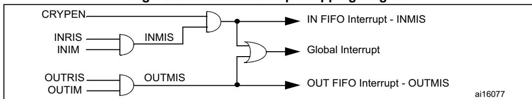
There are two individual maskable interrupt sources generated by the CRYP. These two sources are combined into a single interrupt signal, which is the only interrupt signal from the CRYP that drives the NVIC (nested vectored interrupt controller). This combined interrupt, which is an OR function of the individual masked sources, is asserted if any of the individual interrupts listed below is asserted and enabled.
You can enable or disable the interrupt sources individually by changing the mask bits in the CRYP_IMSCR register. Setting the appropriate mask bit to '1' enables the interrupt.
The status of the individual interrupt sources can be read either from the CRYP_RISR register, for raw interrupt status, or from the CRYP_MISR register, for the masked interrupt status.
Output FIFO service interrupt - OUTMIS
The output FIFO service interrupt is asserted when there is one or more (32-bit word) data items in the output FIFO. This interrupt is cleared by reading data from the output FIFO until there is no valid (32-bit) word left (that is, the interrupt follows the state of the OFNE (output FIFO not empty) flag).
The output FIFO service interrupt OUTMIS is NOT enabled with the CRYP enable bit. Consequently, disabling the CRYP does not force the OUTMIS signal low if the output FIFO is not enabled.
Input FIFO service interrupt - INMIS
The input FIFO service interrupt is asserted when there are less than four words in the input FIFO. It is cleared by performing write operations to the input FIFO until it holds four or more words.
The input FIFO service interrupt INMIS is enabled with the CRYP enable bit. Consequently, when CRYP is disabled, the INMIS signal is low even if the input FIFO is empty.
Figure 231. CRYP interrupt mapping diagram
graph LR
    INRIS --> AND1[AND]
    INIM --> AND1
    AND1 -- INMIS --> OR1[OR]
    OUTRIS --> AND2[AND]
    OUTIM --> AND2
    AND2 -- OUTMIS --> OR1
    OR1 --> AND3[AND]
    CRYPEN --> AND3
    AND3 --> GlobalInterrupt[Global Interrupt]
    AND1 --> INFIFO[IN FIFO Interrupt - INMIS]
    AND2 --> OUTFIFO[OUT FIFO Interrupt - OUTMIS]
23.5 CRYP DMA interface
The cryptographic processor provides an interface to connect to the DMA controller. The DMA operation is controlled through the CRYP DMA control register, CRYP_DMACR.
The burst and single transfer request signals are not mutually exclusive. They can both be asserted at the same time. For example, when there are 6 words available in the OUT FIFO, the burst transfer request and the single transfer request are asserted. After a burst transfer of 4 words, the single transfer request only is asserted to transfer the last 2 available words. This is useful for situations where the number of words left to be received in the stream is less than a burst.
Each request signal remains asserted until the relevant DMA clear signal is asserted. After the request clear signal is deasserted, a request signal can become active again, depending on the above described conditions. All request signals are deasserted if the CRYP peripheral is disabled or the DMA enable bit is cleared (DIEN bit for the IN FIFO and DOEN bit for the OUT FIFO in the CRYP_DMACR register).
Note: The DMA controller must be configured to perform burst of 4 words or less. Otherwise some data could be lost.
In order to let the DMA controller empty the OUT FIFO before filling up the IN FIFO, the OUTDMA channel should have a higher priority than the INDMA channel.
23.6 CRYP registers
The cryptographic core is associated with several control and status registers, eight key registers and four initialization vectors registers.
23.6.1 CRYP control register (CRYP_CR) for STM32F415/417xx
Address offset: 0x00
Reset value: 0x0000 0000
| 31 | 30 | 29 | 28 | 27 | 26 | 25 | 24 | 23 | 22 | 21 | 20 | 19 | 18 | 17 | 16 |
|---|---|---|---|---|---|---|---|---|---|---|---|---|---|---|---|
| Reserved | |||||||||||||||
| 15 | 14 | 13 | 12 | 11 | 10 | 9 | 8 | 7 | 6 | 5 | 4 | 3 | 2 | 1 | 0 |
| CRYPEN | FFLUSH | Reserved | KEYSIZE | DATATYPE | ALGOMODE[2:0] | ALGODIR | Res. | Res. | |||||||
| rw | w | rw | rw | rw | rw | rw | rw | rw | rw | ||||||
Bits 31:18 Reserved, must be kept at reset value
Bits 17:16 Reserved, must be kept at reset value
Bit 15 CRYPEN : Cryptographic processor enable
0: CRYP processor is disabled
1: CRYP processor is enabled
Note: The CRYPEN bit is automatically cleared by hardware when the key preparation process ends (ALGOMODE=111b) or GCM_CCM init Phase
Bit 14 FFLUSH : FIFO flush
When CRYPEN = 0, writing this bit to 1 flushes the IN and OUT FIFOs (that is read and write pointers of the FIFOs are reset. Writing this bit to 0 has no effect.
When CRYPEN = 1, writing this bit to 0 or 1 has no effect.
Reading this bit always returns 0.
Bits 13:10 Reserved, must be kept at reset value
Bits 9:8 KEYSIZE[1:0] : Key size selection (AES mode only)
This bitfield defines the bit-length of the key used for the AES cryptographic core. This bitfield is 'don't care' in the DES or TDES modes.
00: 128 bit key length
01: 192 bit key length
10: 256 bit key length
11: Reserved, do not use this value
Bits 7:6 DATATYPE[1:0] : Data type selection
This bitfield defines the format of data entered in the CRYP_DIN register (refer to Section 23.3.3: Data type ).
00: 32-bit data. No swapping of each word. First word pushed into the IN FIFO (or popped off the OUT FIFO) forms bits 1...32 of the data block, the second word forms bits 33...64.
01: 16-bit data, or half-word. Each word pushed into the IN FIFO (or popped off the OUT FIFO) is considered as 2 half-words, which are swapped with each other.
10: 8-bit data, or bytes. Each word pushed into the IN FIFO (or popped off the OUT FIFO) is considered as 4 bytes, which are swapped with each other.
11: bit data, or bit-string. Each word pushed into the IN FIFO (or popped off the OUT FIFO) is considered as 32 bits (1st bit of the string at position 0), which are swapped with each other.
Bits 5:3 ALGOMODE[2:0] : Algorithm mode
000: TDES-ECB (triple-DES Electronic codebook): no feedback between blocks of data. Initialization vectors (CRYP_IV0(L/R)) are not used, three key vectors (K1, K2, and K3) are used (K0 is not used).
001: TDES-CBC (triple-DES Cipher block chaining): output block is XORed with the subsequent input block before its entry into the algorithm. Initialization vectors (CRYP_IV0(L/R)) must be initialized, three key vectors (K1, K2, and K3) are used (K0 is not used).
010: DES-ECB (simple DES Electronic codebook): no feedback between blocks of data. Initialization vectors (CRYP_IV0(L/R)) are not used, only one key vector (K1) is used (K0, K2, K3 are not used).
011: DES-CBC (simple DES Cipher block chaining): output block is XORed with the subsequent input block before its entry into the algorithm. Initialization vectors (CRYP_IV0(L/R)) must be initialized. Only one key vector (K1) is used (K0, K2, K3 are not used).
100: AES-ECB (AES Electronic codebook): no feedback between blocks of data. Initialization vectors (CRYP_IV0(L/R)...1(L/R)) are not used. All four key vectors (K0...K3) are used.
101: AES-CBC (AES Cipher block chaining): output block is XORed with the subsequent input block before its entry into the algorithm. Initialization vectors (CRYP_IV0(L/R)...1(L/R)) must be initialized. All four key vectors (K0...K3) are used.
110: AES-CTR (AES counter mode): output block is XORed with the subsequent input block before its entry into the algorithm. Initialization vectors (CRYP_IV0(L/R)...1(L/R)) must be initialized. All four key vectors (K0...K3) are used. CTR decryption does not differ from CTR encryption, since the core always encrypts the current counter block to produce the key stream that is XORed with the plaintext or cipher in input. Thus, ALGODIR is don't care when ALGOMODE = 110b, and the key must NOT be unrolled (prepared) for decryption.
111: AES key preparation for decryption mode. Writing this value when CRYPTEN = 1 immediately starts an AES round for key preparation. The secret key must have previously been loaded into the K0...K3 registers. The BUSY bit in the CRYP_SR register is set during the key preparation. After key processing, the resulting key is copied back into the K0...K3 registers, and the BUSY bit is cleared.
Bit 2 ALGODIR : Algorithm direction
0: Encrypt
1: Decrypt
Bits 1:0 Reserved, must be kept at reset value
Note: Writing to the KEYSIZE, DATATYPE, ALGOMODE and ALGODIR bits while BUSY=1 has no effect. These bits can only be configured when BUSY=0. The FFLUSH bit has to be set only when BUSY=0. If not, the FIFO is flushed, but the block being processed may be pushed into the output FIFO just after the flush operation, resulting in a nonempty FIFO condition.
23.6.2 CRYP control register (CRYP_CR) for STM32F415/417xx
Address offset: 0x00
Reset value: 0x0000 0000
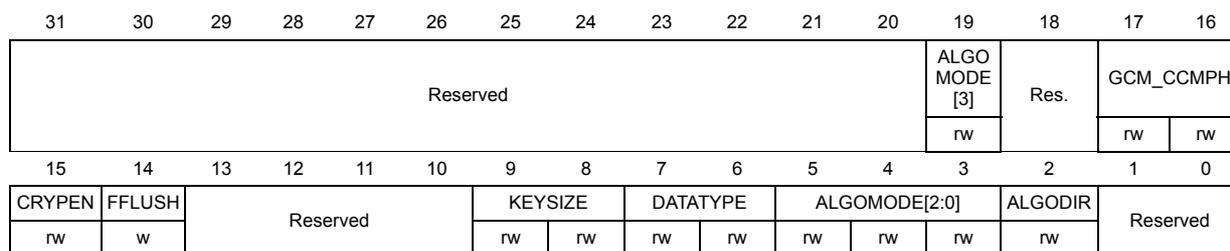
| 31 | 30 | 29 | 28 | 27 | 26 | 25 | 24 | 23 | 22 | 21 | 20 | 19 | 18 | 17 | 16 |
| Reserved | ALGO MODE [3] | Res. | GCM_CCMPH | ||||||||||||
| rw | rw | rw | |||||||||||||
| 15 | 14 | 13 | 12 | 11 | 10 | 9 | 8 | 7 | 6 | 5 | 4 | 3 | 2 | 1 | 0 |
| CRYPEN | FFLUSH | Reserved | KEYSIZE | DATATYPE | ALGOMODE[2:0] | ALGODIR | Reserved | ||||||||
| rw | w | rw | rw | rw | rw | rw | rw | rw | |||||||
Bits 31:20 Reserved, forced by hardware to 0.
Bit 18 Reserved, forced by hardware to 0.
Bits 17:16 GCM_CCMPH[1:0]: no effect if “GCM or CCM algorithm” is not set
00: GCM_CCM init Phase
01: GCM_CCM header phase
10: GCM_CCM payload phase
11: GCM_CCM final phase
Bit 15 CRYPEN : Cryptographic processor enable
0: CRYP processor is disabled
1: CRYP processor is enabled
Note: The CRYPEN bit is automatically cleared by hardware when the key preparation process ends (ALGOMODE=111b) or GCM_CCM init Phase
Bit 14 FFLUSH : FIFO flush
When CRYPEN = 0, writing this bit to 1 flushes the IN and OUT FIFOs (that is read and write pointers of the FIFOs are reset. Writing this bit to 0 has no effect.
When CRYPEN = 1, writing this bit to 0 or 1 has no effect.
Reading this bit always returns 0.
Bits 13:10 Reserved, forced by hardware to 0.
Bits 9:8 KEYSIZE[1:0] : Key size selection (AES mode only)
This bitfield defines the bit-length of the key used for the AES cryptographic core.
This bitfield is ‘don’t care’ in the DES or TDES modes.
00: 128 bit key length
01: 192 bit key length
10: 256 bit key length
11: Reserved, do not use this value
Bits 7:6 DATATYPE[1:0] : Data type selection
This bitfield defines the format of data entered in the CRYP_DIN register (refer to Section 23.3.3: Data type ).
00: 32-bit data. No swapping of each word. First word pushed into the IN FIFO (or popped off the OUT FIFO) forms bits 1...32 of the data block, the second word forms bits 33...64.
01: 16-bit data, or half-word. Each word pushed into the IN FIFO (or popped off the OUT FIFO) is considered as 2 half-words, which are swapped with each other.
10: 8-bit data, or bytes. Each word pushed into the IN FIFO (or popped off the OUT FIFO) is considered as 4 bytes, which are swapped with each other.
11: bit data, or bit-string. Each word pushed into the IN FIFO (or popped off the OUT FIFO) is considered as 32 bits (1st bit of the string at position 0), which are swapped with each other.
Bits 19 and 5:3 ALGOMODE[3:0] : Algorithm mode
0000: TDES-ECB (triple-DES Electronic codebook): no feedback between blocks of data. Initialization vectors (CRYP_IV0(L/R)) are not used, three key vectors (K1, K2, and K3) are used (K0 is not used).
0001: TDES-CBC (triple-DES Cipher block chaining): output block is XORed with the subsequent input block before its entry into the algorithm. Initialization vectors (CRYP_IV0(L/R)) must be initialized, three key vectors (K1, K2, and K3) are used (K0 is not used).
0010: DES-ECB (simple DES Electronic codebook): no feedback between blocks of data. Initialization vectors (CRYP_IV0(L/R)) are not used, only one key vector (K1) is used (K0, K2, K3 are not used).
0011: DES-CBC (simple DES Cipher block chaining): output block is XORed with the subsequent input block before its entry into the algorithm. Initialization vectors (CRYP_IV0(L/R)) must be initialized. Only one key vector (K1) is used (K0, K2, K3 are not used).
0100: AES-ECB (AES Electronic codebook): no feedback between blocks of data. Initialization vectors (CRYP_IV0(L/R)...1L/R)) are not used. All four key vectors (K0...K3) are used.
0101: AES-CBC (AES Cipher block chaining): output block is XORed with the subsequent input block before its entry into the algorithm. Initialization vectors (CRYP_IV0(L/R)...1L/R)) must be initialized. All four key vectors (K0...K3) are used.
0110: AES-CTR (AES Counter mode): output block is XORed with the subsequent input block before its entry into the algorithm. Initialization vectors (CRYP_IV0(L/R)...1L/R)) must be initialized. All four key vectors (K0...K3) are used. CTR decryption does not differ from CTR encryption, since the core always encrypts the current counter block to produce the key stream that is XORed with the plaintext or cipher in input. Thus, ALGODIR is don't care when ALGOMODE = 110b, and the key must NOT be unrolled (prepared) for decryption.
0111: AES key preparation for decryption mode. Writing this value when CRYPTEN = 1 immediately starts an AES round for key preparation. The secret key must have previously been loaded into the K0...K3 registers. The BUSY bit in the CRYP_SR register is set during the key preparation. After key processing, the resulting key is copied back into the K0...K3 registers, and the BUSY bit is cleared.
1000: Galois Counter Mode (GCM). This algorithm mode is also used for the GMAC algorithm.
1001: Counter with CBC-MAC (CCM). This algorithm mode is also used for the CMAC algorithm.
Bit 2 ALGODIR : Algorithm direction
0: Encrypt
1: Decrypt
Bits 1:0 Reserved, must be kept to 0.
Note:
Writing to the
KEYSIZE
,
DATATYPE
,
ALGOMODE
and
ALGODIR
bits while
BUSY=1
has no effect. These bits can only be configured when
BUSY=0
.
The
FFLUSH
bit has to be set only when
BUSY=0
. If not, the FIFO is flushed, but the block being processed may be pushed into the output FIFO just after the flush operation, resulting in a nonempty FIFO condition.
23.6.3 CRYP status register (CRYP_SR)
Address offset: 0x04
Reset value: 0x0000 0003
| 31 | 30 | 29 | 28 | 27 | 26 | 25 | 24 | 23 | 22 | 21 | 20 | 19 | 18 | 17 | 16 |
| Reserved | |||||||||||||||
| 15 | 14 | 13 | 12 | 11 | 10 | 9 | 8 | 7 | 6 | 5 | 4 | 3 | 2 | 1 | 0 |
| Reserved | BUSY | OFFU | OFNE | IFNF | IFEM | ||||||||||
| r | r | r | r | r | |||||||||||
Bits 31:5 Reserved, must be kept at reset value
Bit 4 BUSY : Busy bit
0: The CRYP Core is not processing any data. The reason is either that:
- – the CRYP core is disabled (CRYPEN=0 in the CRYP_CR register) and the last processing has completed, or
- – The CRYP core is waiting for enough data in the input FIFO or enough free space in the output FIFO (that is in each case at least 2 words in the DES, 4 words in the AES).
1: The CRYP core is currently processing a block of data or a key preparation (for AES decryption).
Bit 3 OFFU : Output FIFO full
0: Output FIFO is not full
1: Output FIFO is full
Bit 2 OFNE : Output FIFO not empty
0: Output FIFO is empty
1: Output FIFO is not empty
Bit 1 IFNF : Input FIFO not full
0: Input FIFO is full
1: Input FIFO is not full
Bit 0 IFEM : Input FIFO empty
0: Input FIFO is not empty
1: Input FIFO is empty
23.6.4 CRYP data input register (CRYP_DIN)
Address offset: 0x08
Reset value: 0x0000 0000
The CRYP_DIN register is the data input register. It is 32-bit wide. It is used to enter up to four 64-bit (TDES) or two 128-bit (AES) plaintext (when encrypting) or ciphertext (when decrypting) blocks into the input FIFO, one 32-bit word at a time.
The first word written into the FIFO is the MSB of the input block. The LSB of the input block is written at the end. Disregarding the data swapping, this gives:
- • In the DES/TDES modes: a block is a sequence of bits numbered from bit 1 (leftmost bit) to bit 64 (rightmost bit). Bit 1 corresponds to the MSB (bit 31) of the first word entered into the FIFO, bit 64 corresponds to the LSB (bit 0) of the second word entered into the FIFO.
- • In the AES mode: a block is a sequence of bits numbered from 0 (leftmost bit) to 127 (rightmost bit). Bit 0 corresponds to the MSB (bit 31) of the first word written into the FIFO, bit 127 corresponds to the LSB (bit 0) of the 4th word written into the FIFO.
To fit different data sizes, the data written in the CRYP_DIN register can be swapped before being processed by configuring the DATATYPE bits in the CRYP_CR register. Refer to Section 23.3.3: Data type on page 742 for more details.
When CRYP_DIN register is written to, the data are pushed into the input FIFO. When at least two 32-bit words in the DES/TDES mode (or four 32-bit words in the AES mode) have been pushed into the input FIFO, and when at least 2 words are free in the output FIFO, the CRYP engine starts an encrypting or decrypting process. This process takes two 32-bit words in the DES/TDES mode (or four 32-bit words in the AES mode) from the input FIFO and delivers two 32-bit words (or 4, respectively) to the output FIFO per process round.
When CRYP_DIN register is read:
- • If CRYPTEN = 0, the FIFO is popped, and then the data present in the Input FIFO are returned, from the oldest one (first reading) to the newest one (last reading). The IFEM flag must be checked before each read operation to make sure that the FIFO is not empty.
- • if CRYPTEN = 1, an undefined value is returned.
After the CRYP_DIN register has been read once or several times, the FIFO must be flushed by setting the FFLUSH bit prior to processing new data.
| 31 | 30 | 29 | 28 | 27 | 26 | 25 | 24 | 23 | 22 | 21 | 20 | 19 | 18 | 17 | 16 |
| DATAIN | |||||||||||||||
| rw | rw | rw | rw | rw | rw | rw | rw | rw | rw | rw | rw | rw | rw | rw | rw |
| 15 | 14 | 13 | 12 | 11 | 10 | 9 | 8 | 7 | 6 | 5 | 4 | 3 | 2 | 1 | 0 |
| DATAIN | |||||||||||||||
| rw | rw | rw | rw | rw | rw | rw | rw | rw | rw | rw | rw | rw | rw | rw | rw |
Bits 31:0 DATAIN : Data input
Read = returns Input FIFO content if CRYPTEN = 0, else returns an undefined value.
Write = Input FIFO is written.
23.6.5 CRYP data output register (CRYP_DOUT)
Address offset: 0x0C
Reset value: 0x0000 0000
The CRYP_DOUT register is the data output register. It is read-only and 32-bit wide. It is used to retrieve up to four 64-bit (TDES mode) or two 128-bit (AES mode) ciphertext (when encrypting) or plaintext (when decrypting) blocks from the output FIFO, one 32-bit word at a time.
Like for the input data, the MSB of the output block is the first word read from the output FIFO. The LSB of the output block is read at the end. Disregarding data swapping, this gives:
- • In the DES/TDES modes: Bit 1 (leftmost bit) corresponds to the MSB (bit 31) of the first word read from the FIFO, bit 64 (rightmost bit) corresponds to the LSB (bit 0) of the second word read from the FIFO.
- • In the AES mode: Bit 0 (leftmost bit) corresponds to the MSB (bit 31) of the first word read from the FIFO, bit 127 (rightmost bit) corresponds to the LSB (bit 0) of the 4th word read from the FIFO.
To fit different data sizes, the data can be swapped after processing by configuring the DATATYPE bits in the CRYP_CR register. Refer to Section 23.3.3: Data type on page 742 for more details.
When CRYP_DOUT register is read, the last data entered into the output FIFO (pointed to by the read pointer) is returned.
| 31 | 30 | 29 | 28 | 27 | 26 | 25 | 24 | 23 | 22 | 21 | 20 | 19 | 18 | 17 | 16 |
| DATAOUT | |||||||||||||||
| r | r | r | r | r | r | r | r | r | r | r | r | r | r | r | r |
| 15 | 14 | 13 | 12 | 11 | 10 | 9 | 8 | 7 | 6 | 5 | 4 | 3 | 2 | 1 | 0 |
| DATAOUT | |||||||||||||||
| r | r | r | r | r | r | r | r | r | r | r | r | r | r | r | r |
Bits 31:0 DATAOUT : Data output
Read = returns output FIFO content.
Write = No effect.
23.6.6 CRYP DMA control register (CRYP_DMACR)
Address offset: 0x10
Reset value: 0x0000 0000
| 31 | 30 | 29 | 28 | 27 | 26 | 25 | 24 | 23 | 22 | 21 | 20 | 19 | 18 | 17 | 16 |
| Reserved | |||||||||||||||
| 15 | 14 | 13 | 12 | 11 | 10 | 9 | 8 | 7 | 6 | 5 | 4 | 3 | 2 | 1 | 0 |
| Reserved | DOEN | DIEN | |||||||||||||
| rw | rw | ||||||||||||||
Bits 31:2 Reserved, must be kept at reset value
Bit 1 DOEN : DMA output enable
- 0: DMA for outgoing data transfer is disabled
- 1: DMA for outgoing data transfer is enabled
Bit 0 DIEN : DMA input enable
- 0: DMA for incoming data transfer is disabled
- 1: DMA for incoming data transfer is enabled
23.6.7 CRYP interrupt mask set/clear register (CRYP_IMSCR)
Address offset: 0x14
Reset value: 0x0000 0000
The CRYP_IMSCR register is the interrupt mask set or clear register. It is a read/write register. On a read operation, this register gives the current value of the mask on the relevant interrupt. Writing 1 to the particular bit sets the mask, enabling the interrupt to be read. Writing 0 to this bit clears the corresponding mask. All the bits are cleared to 0 when the peripheral is reset.

| 31 | 30 | 29 | 28 | 27 | 26 | 25 | 24 | 23 | 22 | 21 | 20 | 19 | 18 | 17 | 16 |
| Reserved | |||||||||||||||
| 15 | 14 | 13 | 12 | 11 | 10 | 9 | 8 | 7 | 6 | 5 | 4 | 3 | 2 | 1 | 0 |
| Reserved | OUTIM | INIM | |||||||||||||
| rw | rw | ||||||||||||||
Bits 31:2 Reserved, must be kept at reset value
Bit 1 OUTIM : Output FIFO service interrupt mask
- 0: Output FIFO service interrupt is masked
- 1: Output FIFO service interrupt is not masked
Bit 0 INIM : Input FIFO service interrupt mask
- 0: Input FIFO service interrupt is masked
- 1: Input FIFO service interrupt is not masked
23.6.8 CRYP raw interrupt status register (CRYP_RISR)
Address offset: 0x18
Reset value: 0x0000 0001
The CRYP_RISR register is the raw interrupt status register. It is a read-only register. On a read, this register gives the current raw status of the corresponding interrupt prior to masking. A write has no effect.
| 31 | 30 | 29 | 28 | 27 | 26 | 25 | 24 | 23 | 22 | 21 | 20 | 19 | 18 | 17 | 16 |
| Reserved | |||||||||||||||
| 15 | 14 | 13 | 12 | 11 | 10 | 9 | 8 | 7 | 6 | 5 | 4 | 3 | 2 | 1 | 0 |
| Reserved | OUTRIS | INRIS | |||||||||||||
| r | r | r | |||||||||||||
Bits 31:2 Reserved, must be kept at reset value
Bit 1 OUTRIS : Output FIFO service raw interrupt status
Gives the raw interrupt state prior to masking of the output FIFO service interrupt.
0: Raw interrupt not pending
1: Raw interrupt pending
Bit 0 INRIS : Input FIFO service raw interrupt status
Gives the raw interrupt state prior to masking of the Input FIFO service interrupt.
0: Raw interrupt not pending
1: Raw interrupt pending
23.6.9 CRYP masked interrupt status register (CRYP_MISR)
Address offset: 0x1C
Reset value: 0x0000 0000
The CRYP_MISR register is the masked interrupt status register. It is a read-only register. On a read, this register gives the current masked status of the corresponding interrupt prior to masking. A write has no effect.
| 31 | 30 | 29 | 28 | 27 | 26 | 25 | 24 | 23 | 22 | 21 | 20 | 19 | 18 | 17 | 16 |
| Reserved | |||||||||||||||
| 15 | 14 | 13 | 12 | 11 | 10 | 9 | 8 | 7 | 6 | 5 | 4 | 3 | 2 | 1 | 0 |
| Reserved | OUTMIS | INMIS | |||||||||||||
| r | r | r | |||||||||||||
Bits 31:2 Reserved, must be kept at reset value
Bit 1 OUTMIS : Output FIFO service masked interrupt status
Gives the interrupt state after masking of the output FIFO service interrupt.
0: Interrupt not pending
1: Interrupt pending
Bit 0 INMIS : Input FIFO service masked interrupt status
Gives the interrupt state after masking of the input FIFO service interrupt.
0: Interrupt not pending
1: Interrupt pending when CRYPEN = 1
23.6.10 CRYP key registers (CRYP_K0...3(L/R)R)
Address offset: 0x20 to 0x3C
Reset value: 0x0000 0000
These registers contain the cryptographic keys.
In the TDES mode, keys are 64-bit binary values (number from left to right, that is the leftmost bit is bit 1), named K1, K2 and K3 (K0 is not used), each key consists of 56 information bits and 8 parity bits. The parity bits are reserved for error detection purposes and are not used by the current block. Thus, bits 8, 16, 24, 32, 40, 48, 56 and 64 of each 64-bit key value Kx[1:64] are not used.
In the AES mode, the key is considered as a single 128-, 192- or 256-bit long bit sequence, \( k_0k_1k_2\dots k_{127/191/255} \) ( \( k_0 \) being the leftmost bit). The AES key is entered into the registers as follows:
- for AES-128: \( k_0..k_{127} \) corresponds to \( b_{127}..b_0 \) ( \( b_{255}..b_{128} \) are not used),
- for AES-192: \( k_0..k_{191} \) corresponds to \( b_{191}..b_0 \) ( \( b_{255}..b_{192} \) are not used),
- for AES-256: \( k_0..k_{255} \) corresponds to \( b_{255}..b_0 \) .
In any case \( b_0 \) is the rightmost bit.
CRYP_K0LR (address offset: 0x20)
| 31 | 30 | 29 | 28 | 27 | 26 | 25 | 24 | 23 | 22 | 21 | 20 | 19 | 18 | 17 | 16 |
|---|---|---|---|---|---|---|---|---|---|---|---|---|---|---|---|
| b255 | b254 | b253 | b252 | b251 | b250 | b249 | b248 | b247 | b246 | b245 | b244 | b243 | b242 | b241 | b240 |
| w | w | w | w | w | w | w | w | w | w | w | w | w | w | w | w |
| 15 | 14 | 13 | 12 | 11 | 10 | 9 | 8 | 7 | 6 | 5 | 4 | 3 | 2 | 1 | 0 |
| b239 | b238 | b237 | b236 | b235 | b234 | b233 | b232 | b231 | b230 | b229 | b228 | b227 | b226 | b225 | b224 |
| w | w | w | w | w | w | w | w | w | w | w | w | w | w | w | w |
CRYP_K0RR (address offset: 0x24)
| 31 | 30 | 29 | 28 | 27 | 26 | 25 | 24 | 23 | 22 | 21 | 20 | 19 | 18 | 17 | 16 |
|---|---|---|---|---|---|---|---|---|---|---|---|---|---|---|---|
| b223 | b222 | b221 | b220 | b219 | b218 | b217 | b216 | b215 | b214 | b213 | b212 | b211 | b210 | b209 | b208 |
| w | w | w | w | w | w | w | w | w | w | w | w | w | w | w | w |
| 15 | 14 | 13 | 12 | 11 | 10 | 9 | 8 | 7 | 6 | 5 | 4 | 3 | 2 | 1 | 0 |
| b207 | b206 | b205 | b204 | b203 | b202 | b201 | b200 | b199 | b198 | b197 | b196 | b195 | b194 | b193 | b192 |
| w | w | w | w | w | w | w | w | w | w | w | w | w | w | w | w |
| 31 | 30 | 29 | 28 | 27 | 26 | 25 | 24 | 23 | 22 | 21 | 20 | 19 | 18 | 17 | 16 |
|---|---|---|---|---|---|---|---|---|---|---|---|---|---|---|---|
| k1.1 b191 | k1.2 b190 | k1.3 b189 | k1.4 b188 | k1.5 b187 | k1.6 b186 | k1.7 b185 | k1.8 b184 | k1.9 b183 | k1.10 b182 | k1.11 b181 | k1.12 b180 | k1.13 b179 | k1.14 b178 | k1.15 b177 | k1.16 b176 |
| w | w | w | w | w | w | w | w | w | w | w | w | w | w | w | w |
| 15 | 14 | 13 | 12 | 11 | 10 | 9 | 8 | 7 | 6 | 5 | 4 | 3 | 2 | 1 | 0 |
| k1.17 b175 | k1.18 b174 | k1.19 b173 | k1.20 b172 | k1.21 b171 | k1.22 b170 | k1.23 b169 | k1.24 b168 | k1.25 b167 | k1.26 b166 | k1.27 b165 | k1.28 b164 | k1.29 b163 | k1.30 b162 | k1.31 b161 | k1.32 b160 |
| w | w | w | w | w | w | w | w | w | w | w | w | w | w | w | w |
| 31 | 30 | 29 | 28 | 27 | 26 | 25 | 24 | 23 | 22 | 21 | 20 | 19 | 18 | 17 | 16 |
|---|---|---|---|---|---|---|---|---|---|---|---|---|---|---|---|
| k1.33 b159 | k1.34 b158 | k1.35 b157 | k1.36 b156 | k1.37 b155 | k1.38 b154 | k1.39 b153 | k1.40 b152 | k1.41 b151 | k1.42 b150 | k1.43 b149 | k1.44 b148 | k1.45 b147 | k1.46 b146 | k1.47 b145 | k1.48 b144 |
| w | w | w | w | w | w | w | w | w | w | w | w | w | w | w | w |
| 15 | 14 | 13 | 12 | 11 | 10 | 9 | 8 | 7 | 6 | 5 | 4 | 3 | 2 | 1 | 0 |
| k1.49 b143 | k1.50 b142 | k1.51 b141 | k1.52 b140 | k1.53 b139 | k1.54 b138 | k1.55 b137 | k1.56 b136 | k1.57 b135 | k1.58 b134 | k1.59 b133 | k1.60 b132 | k1.61 b131 | k1.62 b130 | k1.63 b129 | k1.64 b128 |
| w | w | w | w | w | w | w | w | w | w | w | w | w | w | w | w |
| 31 | 30 | 29 | 28 | 27 | 26 | 25 | 24 | 23 | 22 | 21 | 20 | 19 | 18 | 17 | 16 |
|---|---|---|---|---|---|---|---|---|---|---|---|---|---|---|---|
| k2.1 b127 | k2.2 b126 | k2.3 b125 | k2.4 b124 | k2.5 b123 | k2.6 b122 | k2.7 b121 | k2.8 b120 | k2.9 b119 | k2.10 b118 | k2.11 b117 | k2.12 b116 | k2.13 b115 | k2.14 b114 | k2.15 b113 | k2.16 b112 |
| w | w | w | w | w | w | w | w | w | w | w | w | w | w | w | w |
| 15 | 14 | 13 | 12 | 11 | 10 | 9 | 8 | 7 | 6 | 5 | 4 | 3 | 2 | 1 | 0 |
| k2.17 b111 | k2.18 b110 | k2.19 b109 | k2.20 b108 | k2.21 b107 | k2.22 b106 | k2.23 b105 | k2.24 b104 | k2.25 b103 | k2.26 b102 | k2.27 b101 | k2.28 b100 | k2.29 b99 | k2.30 b98 | k2.31 b97 | k2.32 b96 |
| w | w | w | w | w | w | w | w | w | w | w | w | w | w | w | w |
| 31 | 30 | 29 | 28 | 27 | 26 | 25 | 24 | 23 | 22 | 21 | 20 | 19 | 18 | 17 | 16 |
|---|---|---|---|---|---|---|---|---|---|---|---|---|---|---|---|
| k2.33 b95 | k2.34 b94 | k2.35 b93 | k2.36 b92 | k2.37 b91 | k2.38 b90 | k2.39 b89 | k2.40 b88 | k2.41 b87 | k2.42 b86 | k2.43 b85 | k2.44 b84 | k2.45 b83 | k2.46 b82 | k2.47 b81 | k2.48 b80 |
| w | w | w | w | w | w | w | w | w | w | w | w | w | w | w | w |
| 15 | 14 | 13 | 12 | 11 | 10 | 9 | 8 | 7 | 6 | 5 | 4 | 3 | 2 | 1 | 0 |
| k2.49 b79 | k2.50 b78 | k2.51 b77 | k2.52 b76 | k2.53 b75 | k2.54 b74 | k2.55 b73 | k2.56 b72 | k2.57 b71 | k2.58 b70 | k2.59 b69 | k2.60 b68 | k2.61 b67 | k2.62 b66 | k2.63 b65 | k2.64 b64 |
| w | w | w | w | w | w | w | w | w | w | w | w | w | w | w | w |
| 31 | 30 | 29 | 28 | 27 | 26 | 25 | 24 | 23 | 22 | 21 | 20 | 19 | 18 | 17 | 16 |
|---|---|---|---|---|---|---|---|---|---|---|---|---|---|---|---|
| k3.1 b63 | k3.2 b62 | k3.3 b61 | k3.4 b60 | k3.5 b59 | k3.6 b58 | k3.7 b57 | k3.8 b56 | k3.9 b55 | k3.10 b54 | k3.11 b53 | k3.12 b52 | k3.13 b51 | k3.14 b50 | k3.15 b49 | k3.16 b48 |
| w | w | w | w | w | w | w | w | w | w | w | w | w | w | w | w |
| 15 | 14 | 13 | 12 | 11 | 10 | 9 | 8 | 7 | 6 | 5 | 4 | 3 | 2 | 1 | 0 |
| k3.17 b47 | k3.18 b46 | k3.19 b45 | k3.20 b44 | k3.21 b43 | k3.22 b42 | k3.23 b41 | k3.24 b40 | k3.25 b39 | k3.26 b38 | k3.27 b37 | k3.28 b36 | k3.29 b35 | k3.30 b34 | k3.31 b33 | k3.32 b32 |
| w | w | w | w | w | w | w | w | w | w | w | w | w | w | w | w |
| 31 | 30 | 29 | 28 | 27 | 26 | 25 | 24 | 23 | 22 | 21 | 20 | 19 | 18 | 17 | 16 |
|---|---|---|---|---|---|---|---|---|---|---|---|---|---|---|---|
| k3.33 b31 | k3.34 b30 | k3.35 b29 | k3.36 b28 | k3.37 b27 | k3.38 b26 | k3.39 b25 | k3.40 b24 | k3.41 b23 | k3.42 b22 | k3.43 b21 | k3.44 b20 | k3.45 b19 | k3.46 b18 | k3.47 b17 | k3.48 b16 |
| w | w | w | w | w | w | w | w | w | w | w | w | w | w | w | w |
| 15 | 14 | 13 | 12 | 11 | 10 | 9 | 8 | 7 | 6 | 5 | 4 | 3 | 2 | 1 | 0 |
| k3.49 b15 | k3.50 b14 | k3.51 b13 | k3.52 b12 | k3.53 b11 | k3.54 b10 | k3.55 b9 | k3.56 b8 | k3.57 b7 | k3.58 b6 | k3.59 b5 | k3.60 b4 | k3.61 b3 | k3.62 b2 | k3.63 b1 | k3.64 b0 |
| w | w | w | w | w | w | w | w | w | w | w | w | w | w | w | w |
Note: Write accesses to these registers are disregarded when the cryptographic processor is busy (bit BUSY = 1 in the CRYP_SR register).
23.6.11 CRYP initialization vector registers (CRYP_IV0...1(L/R)R)Address offset: 0x40 to 0x4C
Reset value: 0x0000 0000
The CRYP_IV0...1(L/R)R are the left-word and right-word registers for the initialization vector (64 bits for DES/TDES and 128 bits for AES) and are used in the CBC (Cipher block chaining) and Counter (CTR) modes. After each computation round of the TDES or AES Core, the CRYP_IV0...1(L/R)R registers are updated as described in Section : DES and TDES Cipher block chaining (DES/TDES-CBC) mode on page 729 , Section : AES Cipher block chaining (AES-CBC) mode on page 733 and Section : AES counter mode (AES-CTR) mode on page 735 .
IV0 is the leftmost bit whereas IV63 (DES, TDES) or IV127 (AES) are the rightmost bits of the initialization vector. IV1(L/R)R is used only in the AES.
CRYP_IV0LR (address offset: 0x40)| 31 | 30 | 29 | 28 | 27 | 26 | 25 | 24 | 23 | 22 | 21 | 20 | 19 | 18 | 17 | 16 |
|---|---|---|---|---|---|---|---|---|---|---|---|---|---|---|---|
| IV0 | IV1 | IV2 | IV3 | IV4 | IV5 | IV6 | IV7 | IV8 | IV9 | IV10 | IV11 | IV12 | IV13 | IV14 | IV15 |
| rw | rw | rw | rw | rw | rw | rw | rw | rw | rw | rw | rw | rw | rw | rw | rw |
| 15 | 14 | 13 | 12 | 11 | 10 | 9 | 8 | 7 | 6 | 5 | 4 | 3 | 2 | 1 | 0 |
| IV16 | IV17 | IV18 | IV19 | IV20 | IV21 | IV22 | IV23 | IV24 | IV25 | IV26 | IV27 | IV28 | IV29 | IV30 | IV31 |
| rw | rw | rw | rw | rw | rw | rw | rw | rw | rw | rw | rw | rw | rw | rw | rw |
| 31 | 30 | 29 | 28 | 27 | 26 | 25 | 24 | 23 | 22 | 21 | 20 | 19 | 18 | 17 | 16 |
|---|---|---|---|---|---|---|---|---|---|---|---|---|---|---|---|
| IV32 | IV33 | IV34 | IV35 | IV36 | IV37 | IV38 | IV39 | IV40 | IV41 | IV42 | IV43 | IV44 | IV45 | IV46 | IV47 |
| rw | rw | rw | rw | rw | rw | rw | rw | rw | rw | rw | rw | rw | rw | rw | rw |
| 15 | 14 | 13 | 12 | 11 | 10 | 9 | 8 | 7 | 6 | 5 | 4 | 3 | 2 | 1 | 0 |
| IV48 | IV49 | IV50 | IV51 | IV52 | IV53 | IV54 | IV55 | IV56 | IV57 | IV58 | IV59 | IV60 | IV61 | IV62 | IV63 |
| rw | rw | rw | rw | rw | rw | rw | rw | rw | rw | rw | rw | rw | rw | rw | rw |
CRYP_IV1LR (address offset: 0x48)
| 31 | 30 | 29 | 28 | 27 | 26 | 25 | 24 | 23 | 22 | 21 | 20 | 19 | 18 | 17 | 16 |
|---|---|---|---|---|---|---|---|---|---|---|---|---|---|---|---|
| IV64 | IV65 | IV66 | IV67 | IV68 | IV69 | IV70 | IV71 | IV72 | IV73 | IV74 | IV75 | IV76 | IV77 | IV78 | IV79 |
| rw | rw | rw | rw | rw | rw | rw | rw | rw | rw | rw | rw | rw | rw | rw | rw |
| 15 | 14 | 13 | 12 | 11 | 10 | 9 | 8 | 7 | 6 | 5 | 4 | 3 | 2 | 1 | 0 |
| IV80 | IV81 | IV82 | IV83 | IV84 | IV85 | IV86 | IV87 | IV88 | IV89 | IV90 | IV91 | IV92 | IV93 | IV94 | IV95 |
| rw | rw | rw | rw | rw | rw | rw | rw | rw | rw | rw | rw | rw | rw | rw | rw |
CRYP_IV1RR (address offset: 0x4C)
| 31 | 30 | 29 | 28 | 27 | 26 | 25 | 24 | 23 | 22 | 21 | 20 | 19 | 18 | 17 | 16 |
|---|---|---|---|---|---|---|---|---|---|---|---|---|---|---|---|
| IV96 | IV97 | IV98 | IV99 | IV100 | IV101 | IV102 | IV103 | IV104 | IV105 | IV106 | IV107 | IV108 | IV109 | IV110 | IV111 |
| rw | rw | rw | rw | rw | rw | rw | rw | rw | rw | rw | rw | rw | rw | rw | rw |
| 15 | 14 | 13 | 12 | 11 | 10 | 9 | 8 | 7 | 6 | 5 | 4 | 3 | 2 | 1 | 0 |
| IV112 | IV113 | IV114 | IV115 | IV116 | IV117 | IV118 | IV119 | IV120 | IV121 | IV122 | IV123 | IV124 | IV125 | IV126 | IV127 |
| rw | rw | rw | rw | rw | rw | rw | rw | rw | rw | rw | rw | rw | rw | rw | rw |
Note: In DES/3DES modes, only CRYP_IV0(L/R) is used.
Write access to these registers are disregarded when the cryptographic processor is busy (bit BUSY = 1 in the CRYP_SR register).
23.6.12 CRYP context swap registers (CRYP_CSGCMCCM0..7R and CRYP_CSGCM0..7R) for STM32F42xxx and STM32F43xxx
Address offset:
- • CRYP_CSGCMCCM0..7: 0x050 to 0x06C: used for GCM/GMAC or CCM/CMAC alogrithm only
- • CRYP_CSGCM0..7: 0x070 to 0x08C: used for GCM/GMAC algorithm only
Reset value: 0x0000 0000
These registers contain the complete internal register states of the CRYP processor when the GCM/GMAC or CCM/CMAC algorithm is selected. They are useful when a context swap has to be performed because a high-priority task needs the cryptographic processor while it is already in use by another task.
When such an event occurs, the CRYP_CSGCMCCM0..7R and CRYP_CSGCM0..7R (in GCM/GMAC mode) or CRYP_CSGCMCCM0..7R (in CCM/CMAC mode) registers have to be read and the values retrieved have to be saved in the system memory space. The cryptographic processor can then be used by the preemptive task, and when the cryptographic computation is complete, the saved context can be read from memory and written back into the corresponding context swap registers.
Note: These registers are used only when GCM/GMAC or CCM/CMAC algorithm mode is selected.
CRYP_CSGCMCCMxR: where x=[7:0]
| 31 | 30 | 29 | 28 | 27 | 26 | 25 | 24 | 23 | 22 | 21 | 20 | 19 | 18 | 17 | 16 |
|---|---|---|---|---|---|---|---|---|---|---|---|---|---|---|---|
| CRYP_CSGCMCCMxR | |||||||||||||||
| rw | rw | rw | rw | rw | rw | rw | rw | rw | rw | rw | rw | rw | rw | rw | rw |
| 15 | 14 | 13 | 12 | 11 | 10 | 9 | 8 | 7 | 6 | 5 | 4 | 3 | 2 | 1 | 0 |
| CRYP_CSGCMCCMxR | |||||||||||||||
| rw | rw | rw | rw | rw | rw | rw | rw | rw | rw | rw | rw | rw | rw | rw | rw |
CRYP_CSGCMxR: where x=[7:0]
| 31 | 30 | 29 | 28 | 27 | 26 | 25 | 24 | 23 | 22 | 21 | 20 | 19 | 18 | 17 | 16 |
|---|---|---|---|---|---|---|---|---|---|---|---|---|---|---|---|
| CRYP_CSGCMxR | |||||||||||||||
| rw | rw | rw | rw | rw | rw | rw | rw | rw | rw | rw | rw | rw | rw | rw | rw |
| 15 | 14 | 13 | 12 | 11 | 10 | 9 | 8 | 7 | 6 | 5 | 4 | 3 | 2 | 1 | 0 |
| CRYP_CSGCMxR | |||||||||||||||
| rw | rw | rw | rw | rw | rw | rw | rw | rw | rw | rw | rw | rw | rw | rw | rw |
23.6.13 CRYP register map
Table 115. CRYP register map and reset values for STM32F415/417xx
| Offset | Register name and reset value | 31 | 30 | 29 | 28 | 27 | 26 | 25 | 24 | 23 | 22 | 21 | 20 | 19 | 18 | 17 | 16 | 15 | 14 | 13 | 12 | 11 | 10 | 9 | 8 | 7 | 6 | 5 | 4 | 3 | 2 | 1 | 0 |
|---|---|---|---|---|---|---|---|---|---|---|---|---|---|---|---|---|---|---|---|---|---|---|---|---|---|---|---|---|---|---|---|---|---|
| 0x00 0x00 | CRYP_CR | Reserved | CRYPEN | FFLUSH | Reserved | KEYSIZE | DATATYPE | ALOMODE[2:0] | ALGODIR | Res. | |||||||||||||||||||||||
| Reset value | 0 | 0 | 0 | 0 | 0 | 0 | 0 | 0 | 0 | 0 | |||||||||||||||||||||||
| 0x04 | CRYP_SR | Reserved | BUSY | OFFU | OFNE | IFNF | IFEM | ||||||||||||||||||||||||||
| Reset value | 0 | 0 | 0 | 1 | 1 | ||||||||||||||||||||||||||||
| 0x08 | CRYP_DIN | DATAIN | |||||||||||||||||||||||||||||||
| Reset value | 0 | 0 | 0 | 0 | 0 | 0 | 0 | 0 | 0 | 0 | 0 | 0 | |||||||||||||||||||||
| 0x0C | CRYP_DOUT | DATAOUT | |||||||||||||||||||||||||||||||
| Reset value | 0 | 0 | 0 | 0 | 0 | 0 | 0 | 0 | 0 | 0 | 0 | 0 | |||||||||||||||||||||
| 0x10 | CRYP_DMACR | Reserved | DOEN | DIEN | |||||||||||||||||||||||||||||
| Reset value | 0 | 0 | |||||||||||||||||||||||||||||||
| 0x14 | CRYP_IMSCR | Reserved | OUTIM | INIM | |||||||||||||||||||||||||||||
| Reset value | 0 | 0 | |||||||||||||||||||||||||||||||
| 0x18 | CRYP_RISR | Reserved | OUTRIS | INRIS | |||||||||||||||||||||||||||||
| Reset value | 0 | 1 | |||||||||||||||||||||||||||||||
| 0x1C | CRYP_MISR | Reserved | OUTMIS | IN%IS | |||||||||||||||||||||||||||||
| Reset value | 0 | 0 | |||||||||||||||||||||||||||||||
| 0x20 | CRYP_K0LR | CRYP_K0LR | |||||||||||||||||||||||||||||||
| Reset value | 0 | 0 | 0 | 0 | 0 | 0 | 0 | 0 | 0 | 0 | 0 | 0 | 0 | 0 | 0 | 0 | 0 | 0 | 0 | 0 | 0 | 0 | 0 | 0 | 0 | 0 | 0 | 0 | 0 | 0 | 0 | 0 | |
| 0x24 | CRYP_K0RR | CRYP_K0RR | |||||||||||||||||||||||||||||||
| Reset value | 0 | 0 | 0 | 0 | 0 | 0 | 0 | 0 | 0 | 0 | 0 | 0 | 0 | 0 | 0 | 0 | 0 | 0 | 0 | 0 | 0 | 0 | 0 | 0 | 0 | 0 | 0 | 0 | 0 | 0 | 0 | 0 | |
| ... | |||||||||||||||||||||||||||||||||
| 0x38 | CRYP_K3LR | CRYP_K3LR | |||||||||||||||||||||||||||||||
| Reset value | 0 | 0 | 0 | 0 | 0 | 0 | 0 | 0 | 0 | 0 | 0 | 0 | 0 | 0 | 0 | 0 | 0 | 0 | 0 | 0 | 0 | 0 | 0 | 0 | 0 | 0 | 0 | 0 | 0 | 0 | 0 | 0 | |
| 0x3C | CRYP_K3RR | CRYP_K3RR | |||||||||||||||||||||||||||||||
| Reset value | 0 | 0 | 0 | 0 | 0 | 0 | 0 | 0 | 0 | 0 | 0 | 0 | 0 | 0 | 0 | 0 | 0 | 0 | 0 | 0 | 0 | 0 | 0 | 0 | 0 | 0 | 0 | 0 | 0 | 0 | 0 | 0 | |
| 0x40 | CRYP_IV0LR | CRYP_IV0LR | |||||||||||||||||||||||||||||||
| Reset value | 0 | 0 | 0 | 0 | 0 | 0 | 0 | 0 | 0 | 0 | 0 | 0 | 0 | 0 | 0 | 0 | 0 | 0 | 0 | 0 | 0 | 0 | 0 | 0 | 0 | 0 | 0 | 0 | 0 | 0 | 0 | 0 | |
Table 115. CRYP register map and reset values for STM32F415/417xx (continued)
| Offset | Register name and reset value | 31 | 30 | 29 | 28 | 27 | 26 | 25 | 24 | 23 | 22 | 21 | 20 | 19 | 18 | 17 | 16 | 15 | 14 | 13 | 12 | 11 | 10 | 9 | 8 | 7 | 6 | 5 | 4 | 3 | 2 | 1 | 0 |
|---|---|---|---|---|---|---|---|---|---|---|---|---|---|---|---|---|---|---|---|---|---|---|---|---|---|---|---|---|---|---|---|---|---|
| 0x44 | CRYP_IV0RR | CRYP_IV0RR | |||||||||||||||||||||||||||||||
| Reset value | 0 | 0 | 0 | 0 | 0 | 0 | 0 | 0 | 0 | 0 | 0 | 0 | 0 | 0 | 0 | 0 | 0 | 0 | 0 | 0 | 0 | 0 | 0 | 0 | 0 | 0 | 0 | 0 | 0 | 0 | 0 | 0 | 0 |
| 0x48 | CRYP_IV1LR | CRYP_IV1LR | |||||||||||||||||||||||||||||||
| Reset value | 0 | 0 | 0 | 0 | 0 | 0 | 0 | 0 | 0 | 0 | 0 | 0 | 0 | 0 | 0 | 0 | 0 | 0 | 0 | 0 | 0 | 0 | 0 | 0 | 0 | 0 | 0 | 0 | 0 | 0 | 0 | 0 | 0 |
| 0x4C | CRYP_IV1RR | CRYP_IV1RR | |||||||||||||||||||||||||||||||
| Reset value | 0 | 0 | 0 | 0 | 0 | 0 | 0 | 0 | 0 | 0 | 0 | 0 | 0 | 0 | 0 | 0 | 0 | 0 | 0 | 0 | 0 | 0 | 0 | 0 | 0 | 0 | 0 | 0 | 0 | 0 | 0 | 0 | 0 |
Table 116. CRYP register map and reset values for STM32F43xxx
| Offset | Register name and reset value | 31 | 30 | 29 | 28 | 27 | 26 | 25 | 24 | 23 | 22 | 21 | 20 | 19 | 18 | 17 | 16 | 15 | 14 | 13 | 12 | 11 | 10 | 9 | 8 | 7 | 6 | 5 | 4 | 3 | 2 | 1 | 0 |
|---|---|---|---|---|---|---|---|---|---|---|---|---|---|---|---|---|---|---|---|---|---|---|---|---|---|---|---|---|---|---|---|---|---|
| 0x00 0x00 | CRYP_CR | Reserved | |||||||||||||||||||||||||||||||
| Reset value | |||||||||||||||||||||||||||||||||
| 0x04 | CRYP_SR | Reserved | |||||||||||||||||||||||||||||||
| Reset value | |||||||||||||||||||||||||||||||||
| 0x08 | CRYP_DIN | DATAIN | |||||||||||||||||||||||||||||||
| Reset value | |||||||||||||||||||||||||||||||||
| 0x0C | CRYP_DOUT | DATAOUT | |||||||||||||||||||||||||||||||
| Reset value | |||||||||||||||||||||||||||||||||
| 0x10 | CRYP_DMACR | Reserved | |||||||||||||||||||||||||||||||
| Reset value | |||||||||||||||||||||||||||||||||
| 0x14 | CRYP_IMSCR | Reserved | |||||||||||||||||||||||||||||||
| Reset value | |||||||||||||||||||||||||||||||||
| 0x18 | CRYP_RISR | Reserved | |||||||||||||||||||||||||||||||
| Reset value | |||||||||||||||||||||||||||||||||
Table 116. CRYP register map and reset values for STM32F43xxx (continued)
| Offset | Register name reset value | 31 | 30 | 29 | 28 | 27 | 26 | 25 | 24 | 23 | 22 | 21 | 20 | 19 | 18 | 17 | 16 | 15 | 14 | 13 | 12 | 11 | 10 | 9 | 8 | 7 | 6 | 5 | 4 | 3 | 2 | 1 | 0 |
|---|---|---|---|---|---|---|---|---|---|---|---|---|---|---|---|---|---|---|---|---|---|---|---|---|---|---|---|---|---|---|---|---|---|
| 0x1C | CRYP_MISR | Reserved | OUTMIS | INMIS | |||||||||||||||||||||||||||||
| Reset value | 0 | 0 | |||||||||||||||||||||||||||||||
| 0x20 | CRYP_K0LR | CRYP_K0LR | |||||||||||||||||||||||||||||||
| Reset value | 0 | 0 | 0 | 0 | 0 | 0 | 0 | 0 | 0 | 0 | 0 | 0 | 0 | 0 | 0 | 0 | 0 | 0 | 0 | 0 | 0 | 0 | 0 | 0 | 0 | 0 | 0 | 0 | 0 | 0 | 0 | 0 | |
| 0x24 | CRYP_K0RR | CRYP_K0RR | |||||||||||||||||||||||||||||||
| Reset value | 0 | 0 | 0 | 0 | 0 | 0 | 0 | 0 | 0 | 0 | 0 | 0 | 0 | 0 | 0 | 0 | 0 | 0 | 0 | 0 | 0 | 0 | 0 | 0 | 0 | 0 | 0 | 0 | 0 | 0 | 0 | 0 | |
| ... ... | |||||||||||||||||||||||||||||||||
| 0x38 | CRYP_K3LR | CRYP_K3LR | |||||||||||||||||||||||||||||||
| Reset value | 0 | 0 | 0 | 0 | 0 | 0 | 0 | 0 | 0 | 0 | 0 | 0 | 0 | 0 | 0 | 0 | 0 | 0 | 0 | 0 | 0 | 0 | 0 | 0 | 0 | 0 | 0 | 0 | 0 | 0 | 0 | 0 | |
| 0x3C | CRYP_K3RR | CRYP_K3RR | |||||||||||||||||||||||||||||||
| Reset value | 0 | 0 | 0 | 0 | 0 | 0 | 0 | 0 | 0 | 0 | 0 | 0 | 0 | 0 | 0 | 0 | 0 | 0 | 0 | 0 | 0 | 0 | 0 | 0 | 0 | 0 | 0 | 0 | 0 | 0 | 0 | 0 | |
| 0x40 | CRYP_IV0LR | CRYP_IV0LR | |||||||||||||||||||||||||||||||
| Reset value | 0 | 0 | 0 | 0 | 0 | 0 | 0 | 0 | 0 | 0 | 0 | 0 | 0 | 0 | 0 | 0 | 0 | 0 | 0 | 0 | 0 | 0 | 0 | 0 | 0 | 0 | 0 | 0 | 0 | 0 | 0 | 0 | |
| 0x44 | CRYP_IV0RR | CRYP_IV0RR | |||||||||||||||||||||||||||||||
| Reset value | 0 | 0 | 0 | 0 | 0 | 0 | 0 | 0 | 0 | 0 | 0 | 0 | 0 | 0 | 0 | 0 | 0 | 0 | 0 | 0 | 0 | 0 | 0 | 0 | 0 | 0 | 0 | 0 | 0 | 0 | 0 | 0 | |
| 0x48 | CRYP_IV1LR | CRYP_IV1LR | |||||||||||||||||||||||||||||||
| Reset value | 0 | 0 | 0 | 0 | 0 | 0 | 0 | 0 | 0 | 0 | 0 | 0 | 0 | 0 | 0 | 0 | 0 | 0 | 0 | 0 | 0 | 0 | 0 | 0 | 0 | 0 | 0 | 0 | 0 | 0 | 0 | 0 | |
| 0x4C | CRYP_IV1RR | CRYP_IV1RR | |||||||||||||||||||||||||||||||
| Reset value | 0 | 0 | 0 | 0 | 0 | 0 | 0 | 0 | 0 | 0 | 0 | 0 | 0 | 0 | 0 | 0 | 0 | 0 | 0 | 0 | 0 | 0 | 0 | 0 | 0 | 0 | 0 | 0 | 0 | 0 | 0 | 0 | |
| 0x50 | CRYP_CSGCMCCMR | CRYP_CSGCMCCM0R | |||||||||||||||||||||||||||||||
| Reset value | 0 | 0 | 0 | 0 | 0 | 0 | 0 | 0 | 0 | 0 | 0 | 0 | 0 | 0 | 0 | 0 | 0 | 0 | 0 | 0 | 0 | 0 | 0 | 0 | 0 | 0 | 0 | 0 | 0 | 0 | 0 | 0 | |
| 0x54 | CRYP_CSGCMCCM1R | CRYP_CSGCMCCM1R | |||||||||||||||||||||||||||||||
| Reset value | 0 | 0 | 0 | 0 | 0 | 0 | 0 | 0 | 0 | 0 | 0 | 0 | 0 | 0 | 0 | 0 | 0 | 0 | 0 | 0 | 0 | 0 | 0 | 0 | 0 | 0 | 0 | 0 | 0 | 0 | 0 | 0 | |
| 0x58 | CRYP_CSGCMCCM2R | CRYP_CSGCMCCM2R | |||||||||||||||||||||||||||||||
| Reset value | 0 | 0 | 0 | 0 | 0 | 0 | 0 | 0 | 0 | 0 | 0 | 0 | 0 | 0 | 0 | 0 | 0 | 0 | 0 | 0 | 0 | 0 | 0 | 0 | 0 | 0 | 0 | 0 | 0 | 0 | 0 | 0 | |
| 0x5C | CRYP_CSGCMCCM3R | CRYP_CSGCMCCM3R | |||||||||||||||||||||||||||||||
| Reset value | 0 | 0 | 0 | 0 | 0 | 0 | 0 | 0 | 0 | 0 | 0 | 0 | 0 | 0 | 0 | 0 | 0 | 0 | 0 | 0 | 0 | 0 | 0 | 0 | 0 | 0 | 0 | 0 | 0 | 0 | 0 | 0 | |
Table 116. CRYP register map and reset values for STM32F43xxx (continued)
| Offset | Register name reset value | 31 | 30 | 29 | 28 | 27 | 26 | 25 | 24 | 23 | 22 | 21 | 20 | 19 | 18 | 17 | 16 | 15 | 14 | 13 | 12 | 11 | 10 | 9 | 8 | 7 | 6 | 5 | 4 | 3 | 2 | 1 | 0 |
|---|---|---|---|---|---|---|---|---|---|---|---|---|---|---|---|---|---|---|---|---|---|---|---|---|---|---|---|---|---|---|---|---|---|
| 0 | 0 | 0 | 0 | 0 | 0 | 0 | 0 | 0 | 0 | 0 | 0 | 0 | 0 | 0 | 0 | 0 | 0 | 0 | 0 | 0 | 0 | 0 | 0 | 0 | 0 | 0 | 0 | 0 | 0 | 0 | 0 | ||
| 0x60 | CRYP_CSGCMCCM4R | CRYP_CSGCMCCM4R | |||||||||||||||||||||||||||||||
| Reset value | 0 | 0 | 0 | 0 | 0 | 0 | 0 | 0 | 0 | 0 | 0 | 0 | 0 | 0 | 0 | 0 | 0 | 0 | 0 | 0 | 0 | 0 | 0 | 0 | 0 | 0 | 0 | 0 | 0 | 0 | 0 | 0 | |
| 0x64 | CRYP_CSGCMCCM5R | CRYP_CSGCMCCM5R | |||||||||||||||||||||||||||||||
| Reset value | 0 | 0 | 0 | 0 | 0 | 0 | 0 | 0 | 0 | 0 | 0 | 0 | 0 | 0 | 0 | 0 | 0 | 0 | 0 | 0 | 0 | 0 | 0 | 0 | 0 | 0 | 0 | 0 | 0 | 0 | 0 | 0 | |
| 0x68 | CRYP_CSGCMCCM6R | CRYP_CSGCMCCM6R | |||||||||||||||||||||||||||||||
| Reset value | 0 | 0 | 0 | 0 | 0 | 0 | 0 | 0 | 0 | 0 | 0 | 0 | 0 | 0 | 0 | 0 | 0 | 0 | 0 | 0 | 0 | 0 | 0 | 0 | 0 | 0 | 0 | 0 | 0 | 0 | 0 | 0 | |
| 0x6C | CRYP_CSGCMCCM7R | CRYP_CSGCMCCM7R | |||||||||||||||||||||||||||||||
| Reset value | 0 | 0 | 0 | 0 | 0 | 0 | 0 | 0 | 0 | 0 | 0 | 0 | 0 | 0 | 0 | 0 | 0 | 0 | 0 | 0 | 0 | 0 | 0 | 0 | 0 | 0 | 0 | 0 | 0 | 0 | 0 | 0 | |
| 0x70 | CRYP_CSGCM0R | CRYP_CSGCM0R | |||||||||||||||||||||||||||||||
| Reset value | 0 | 0 | 0 | 0 | 0 | 0 | 0 | 0 | 0 | 0 | 0 | 0 | 0 | 0 | 0 | 0 | 0 | 0 | 0 | 0 | 0 | 0 | 0 | 0 | 0 | 0 | 0 | 0 | 0 | 0 | 0 | 0 | |
| 0x74 | CRYP_CSGCM1R | CRYP_CSGCM1R | |||||||||||||||||||||||||||||||
| Reset value | 0 | 0 | 0 | 0 | 0 | 0 | 0 | 0 | 0 | 0 | 0 | 0 | 0 | 0 | 0 | 0 | 0 | 0 | 0 | 0 | 0 | 0 | 0 | 0 | 0 | 0 | 0 | 0 | 0 | 0 | 0 | 0 | |
| 0x78 | CRYP_CSGCM2R | CRYP_CSGCM2R | |||||||||||||||||||||||||||||||
| Reset value | 0 | 0 | 0 | 0 | 0 | 0 | 0 | 0 | 0 | 0 | 0 | 0 | 0 | 0 | 0 | 0 | 0 | 0 | 0 | 0 | 0 | 0 | 0 | 0 | 0 | 0 | 0 | 0 | 0 | 0 | 0 | 0 | |
| 0x7C | CRYP_CSGCM3R | CRYP_CSGCM3R | |||||||||||||||||||||||||||||||
| Reset value | 0 | 0 | 0 | 0 | 0 | 0 | 0 | 0 | 0 | 0 | 0 | 0 | 0 | 0 | 0 | 0 | 0 | 0 | 0 | 0 | 0 | 0 | 0 | 0 | 0 | 0 | 0 | 0 | 0 | 0 | 0 | 0 | |
| 0x80 | CRYP_CSGCM4R | CRYP_CSGCM4R | |||||||||||||||||||||||||||||||
| Reset value | 0 | 0 | 0 | 0 | 0 | 0 | 0 | 0 | 0 | 0 | 0 | 0 | 0 | 0 | 0 | 0 | 0 | 0 | 0 | 0 | 0 | 0 | 0 | 0 | 0 | 0 | 0 | 0 | 0 | 0 | 0 | 0 | |
| 0x84 | CRYP_CSGCM5R | CRYP_CSGCM5R | |||||||||||||||||||||||||||||||
| Reset value | 0 | 0 | 0 | 0 | 0 | 0 | 0 | 0 | 0 | 0 | 0 | 0 | 0 | 0 | 0 | 0 | 0 | 0 | 0 | 0 | 0 | 0 | 0 | 0 | 0 | 0 | 0 | 0 | 0 | 0 | 0 | 0 | |
| 0x88 | CRYP_CSGCM6R | CRYP_CSGCM6R | |||||||||||||||||||||||||||||||
| Reset value | 0 | 0 | 0 | 0 | 0 | 0 | 0 | 0 | 0 | 0 | 0 | 0 | 0 | 0 | 0 | 0 | 0 | 0 | 0 | 0 | 0 | 0 | 0 | 0 | 0 | 0 | 0 | 0 | 0 | 0 | 0 | 0 | |
| 0x8C | CRYP_CSGCM7R | CRYP_CSGCM7R | |||||||||||||||||||||||||||||||
| Reset value | 0 | 0 | 0 | 0 | 0 | 0 | 0 | 0 | 0 | 0 | 0 | 0 | 0 | 0 | 0 | 0 | 0 | 0 | 0 | 0 | 0 | 0 | 0 | 0 | 0 | 0 | 0 | 0 | 0 | 0 | 0 | 0 | |