15. Digital camera interface (DCMI)
This section applies to all STM32F4xx devices, unless otherwise specified.
15.1 DCMI introduction
The digital camera is a synchronous parallel interface able to receive a high-speed data flow from an external 8-, 10-, 12- or 14-bit CMOS camera module. It supports different data formats: YCbCr4:2:2/RGB565 progressive video and compressed data (JPEG).
This interface is for use with black & white cameras, X24 and X5 cameras, and it is assumed that all pre-processing like resizing is performed in the camera module.
15.2 DCMI main features
- • 8-, 10-, 12- or 14-bit parallel interface
- • Embedded/external line and frame synchronization
- • Continuous or snapshot mode
- • Crop feature
- • Supports the following data formats:
- – 8/10/12/14- bit progressive video: either monochrome or raw bayer
- – YCbCr 4:2:2 progressive video
- – RGB 565 progressive video
- – Compressed data: JPEG
15.3 DCMI pins
Table 78 shows the DCMI pins.
Table 78. DCMI pins
| Name | Signal type |
|---|---|
| D[0:13] | Data inputs |
| HSYNC | Horizontal synchronization input |
| VSYNC | Vertical synchronization input |
| PIXCLK | Pixel clock input |
15.4 DCMI clocks
The digital camera interface uses two clock domains PIXCLK and HCLK. The signals generated with PIXCLK are sampled on the rising edge of HCLK once they are stable. An enable signal is generated in the HCLK domain, to indicate that data coming from the camera are stable and can be sampled. The minimum PIXCLK period must be higher than 2.5 HCLK periods.
15.5 DCMI functional overview
The digital camera interface is a synchronous parallel interface that can receive high-speed (up to 54 Mbytes/s) data flows. It consists of up to 14 data lines (D13-D0) and a pixel clock line (PIXCLK). The pixel clock has a programmable polarity, so that data can be captured on either the rising or the falling edge of the pixel clock.
The data are packed into a 32-bit data register (DCMI_DR) and then transferred through a general-purpose DMA channel. The image buffer is managed by the DMA, not by the camera interface.
The data received from the camera can be organized in lines/frames (raw YUB/RGB/Bayer modes) or can be a sequence of JPEG images. To enable JPEG image reception, the JPEG bit (bit 3 of DCMI_CR register) must be set.
The data flow is synchronized either by hardware using the optional HSYNC (horizontal synchronization) and VSYNC (vertical synchronization) signals or by synchronization codes embedded in the data flow.
Figure 72 shows the DCMI block diagram.
Figure 72. DCMI block diagram
The block diagram illustrates the internal architecture of the DCMI. At the top, a 'DMA interface' and a 'Control/Status register' are shown. The 'DMA interface' is connected to an 'AHB interface' on the left and has bidirectional connections to the 'Control/Status register' and a 'FIFO/Data formatter' below it. The 'Control/Status register' has bidirectional connections to the 'DMA interface', the 'FIFO/Data formatter', and a 'Data extraction' block. The 'FIFO/Data formatter' is connected to the 'AHB interface', the 'Control/Status register', and the 'Data extraction' block. The 'Data extraction' block is connected to the 'Control/Status register', the 'FIFO/Data formatter', and a 'Synchronizer' block. The 'Synchronizer' block receives external inputs: 'DCMI_PIXCLK', 'DCMI_D[0:13]', 'DCMI_HSYNC', and 'DCMI_VSYNC'. It has bidirectional connections to the 'Data extraction' block and a unidirectional output to the 'FIFO/Data formatter'. The 'AHB interface' is connected to the 'DMA interface' and the 'FIFO/Data formatter'. The entire diagram is enclosed in a box with the identifier 'ai15604b' in the bottom right corner.
Figure 73. Top-level block diagram
![Top-level block diagram of the DCMI. A central block labeled 'DCMI' has several input and output signals. On the left, 'HCLK' enters the block. Below it, 'DCMI_IT' and 'DMA_REQ' exit the block towards an 'Interrupt controller'. On the right, a group of signals labeled 'External interface' enter the block: 'DCMI_D[0:13]' (data bus), 'DCMI_PIXCLK' (pixel clock), 'DCMI_HSYNC' (horizontal synchronization), and 'DCMI_VSYNC' (vertical synchronization). A small code 'ai15603b' is in the bottom right corner.](/RM0090-STM32F405-415-407-417-427-437-429-439/880ae56e0f50127650e6b24033e6aef9_img.jpg)
15.5.1 DMA interface
The DMA interface is active when the CAPTURE bit in the DCMI_CR register is set. A DMA request is generated each time the camera interface receives a complete 32-bit data block in its register.
15.5.2 DCMI physical interface
The interface is composed of 11/13/15/17 inputs. Only the Slave mode is supported.
The camera interface can capture 8-bit, 10-bit, 12-bit or 14-bit data depending on the EDM[1:0] bits in the DCMI_CR register. If less than 14 bits are used, the unused data pins must not be assigned to DCMI interface through GPIO alternate functions.
Table 79. DCMI signals
| Signal name | Signal description | |
|---|---|---|
| 8 bits | D[0..7] | Data |
| 10 bits | D[0..9] | |
| 12 bits | D[0..11] | |
| 14 bits | D[0..13] | |
| PIXCLK | Pixel clock | |
| HSYNC | Horizontal synchronization / Data valid | |
| VSYNC | Vertical synchronization | |
The data are synchronous with PIXCLK and change on the rising/falling edge of the pixel clock depending on the polarity.
The HSYNC signal indicates the start/end of a line.
The VSYNC signal indicates the start/end of a frame
Figure 74. DCMI signal waveforms
![Figure 74. DCMI signal waveforms. The diagram shows four signal lines over time. DCMI_PIXCLK is a periodic square wave. DCMI_DR[0:13] is a 14-bit data bus that changes its value on the falling edges of DCMI_PIXCLK. DCMI_HSYNC is a horizontal sync signal that is active low. DCMI_VSYNC is a vertical sync signal that is active low. The signals are labeled with their names on the left. The diagram is labeled 'ai15606b' in the bottom right corner.](/RM0090-STM32F405-415-407-417-427-437-429-439/3526b393032672a9cc5f039404e38afa_img.jpg)
- 1. The capture edge of DCMI_PIXCLK is the falling edge, the active state of DCMI_HSYNC and DCMI_VSYNC is 1.
- 1. DCMI_HSYNC and DCMI_VSYNC can change states at the same time.
8-bit data
When EDM[1:0] in DCMI_CR are programmed to “00” the interface captures 8 LSB’s at its input (D[0:7]) and stores them as 8-bit data. The D[13:8] inputs are ignored. In this case, to capture a 32-bit word, the camera interface takes four pixel clock cycles.
The first captured data byte is placed in the LSB position in the 32-bit word and the 4 th captured data byte is placed in the MSB position in the 32-bit word. Table 80 gives an example of the positioning of captured data bytes in two 32-bit words.
Table 80. Positioning of captured data bytes in 32-bit words (8-bit width)
| Byte address | 31:24 | 23:16 | 15:8 | 7:0 |
|---|---|---|---|---|
| 0 | D n+3 [7:0] | D n+2 [7:0] | D n+1 [7:0] | D n [7:0] |
| 4 | D n+7 [7:0] | D n+6 [7:0] | D n+5 [7:0] | D n+4 [7:0] |
10-bit data
When EDM[1:0] in DCMI_CR are programmed to “01”, the camera interface captures 10-bit data at its input D[0..9] and stores them as the 10 least significant bits of a 16-bit word. The remaining most significant bits in the DCMI_DR register (bits 11 to 15) are cleared to zero. So, in this case, a 32-bit data word is made up every two pixel clock cycles.
The first captured data are placed in the LSB position in the 32-bit word and the 2 nd captured data are placed in the MSB position in the 32-bit word as shown in Table 81 .
Table 81. Positioning of captured data bytes in 32-bit words (10-bit width)
| Byte address | 31:26 | 25:16 | 15:10 | 9:0 |
|---|---|---|---|---|
| 0 | 0 | D n+1 [9:0] | 0 | D n [9:0] |
| 4 | 0 | D n+3 [9:0] | 0 | D n+2 [9:0] |
12-bit data
When EDM[1:0] in DCMI_CR are programmed to “10”, the camera interface captures the 12-bit data at its input D[0..11] and stores them as the 12 least significant bits of a 16-bit word. The remaining most significant bits are cleared to zero. So, in this case a 32-bit data word is made up every two pixel clock cycles.
The first captured data are placed in the LSB position in the 32-bit word and the 2 nd captured data are placed in the MSB position in the 32-bit word as shown in Table 82 .
Table 82. Positioning of captured data bytes in 32-bit words (12-bit width)
| Byte address | 31:28 | 27:16 | 15:12 | 11:0 |
|---|---|---|---|---|
| 0 | 0 | D n+1 [11:0] | 0 | D n [11:0] |
| 4 | 0 | D n+3 [11:0] | 0 | D n+2 [11:0] |
14-bit data
When EDM[1:0] in DCMI_CR are programmed to “11”, the camera interface captures the 14-bit data at its input D[0..13] and stores them as the 14 least significant bits of a 16-bit word. The remaining most significant bits are cleared to zero. So, in this case a 32-bit data word is made up every two pixel clock cycles.
The first captured data are placed in the LSB position in the 32-bit word and the 2 nd captured data are placed in the MSB position in the 32-bit word as shown in Table 83 .
Table 83. Positioning of captured data bytes in 32-bit words (14-bit width)
| Byte address | 31:30 | 29:16 | 15:14 | 13:0 |
|---|---|---|---|---|
| 0 | 0 | D n+1 [13:0] | 0 | D n [13:0] |
| 4 | 0 | D n+3 [13:0] | 0 | D n+2 [13:0] |
15.5.3 Synchronization
The digital camera interface supports embedded or hardware (HSYNC & VSYNC) synchronization. When embedded synchronization is used, it is up to the digital camera module to make sure that the 0x00 and 0xFF values are used ONLY for synchronization (not in data). Embedded synchronization codes are supported only for the 8-bit parallel data interface width (that is, in the DCMI_CR register, the EDM[1:0] bits should be cleared to “00”).
For compressed data, the DCMI supports only the hardware synchronization mode. In this case, VSYNC is used as a start/end of the image, and HSYNC is used as a Data Valid signal. Figure 75 shows the corresponding timing diagram.
Figure 75. Timing diagram
The timing diagram shows three signal lines over time:
- JPEG data: A sequence of yellow rectangular blocks representing JPEG packet data. The first block is marked as the "Beginning of JPEG stream" and the last as the "End of JPEG stream". A green block at the end is labeled "Padding data at the end of the JPEG stream". A double-headed arrow indicates the "Programmable JPEG packet size".
- DCMI_HSYNC: A square wave signal that pulses low during each JPEG packet data block.
- DCMI_VSYNC: A square wave signal that is low at the start and end of the JPEG stream, and high during the stream.
Three arrows point from the text "Packet dispatching depends on the image content. This results in a variable blanking duration." to the gaps between JPEG packets.
Legend: A yellow square represents "JPEG packet data".
ai15944b
Hardware synchronization mode
In hardware synchronisation mode, the two synchronization signals (HSYNC/VSYNC) are used.
Depending on the camera module/mode, data may be transmitted during horizontal/vertical synchronisation periods. The HSYNC/VSYNC signals act like blanking signals since all the data received during HSYNC/VSYNC active periods are ignored.
In order to correctly transfer images into the DMA/RAM buffer, data transfer is synchronized with the VSYNC signal. When the hardware synchronisation mode is selected, and capture is enabled (CAPTURE bit set in DCMI_CR), data transfer is synchronized with the deactivation of the VSYNC signal (next start of frame).
Transfer can then be continuous, with successive frames transferred by DMA to successive buffers or the same/circular buffer. To allow the DMA management of successive frames, a VSIF (Vertical synchronization interrupt flag) is activated at the end of each frame.
Embedded data synchronization mode
In this synchronisation mode, the data flow is synchronised using 32-bit codes embedded in the data flow. These codes use the 0x00/0xFF values that are not used in data anymore. There are 4 types of codes, all with a 0xFF0000XY format. The embedded synchronization codes are supported only in 8-bit parallel data width capture (in the DCMI_CR register, the EDM[1:0] bits should be programmed to “00”). For other data widths, this mode generates unpredictable results and must not be used.
Note: Camera modules can have 8 such codes (in interleaved mode). For this reason, the interleaved mode is not supported by the camera interface (otherwise, every other half-frame would be discarded).
- • Mode 2
Four embedded codes signal the following events
- – Frame start (FS)
- – Frame end (FE)
- – Line start (LS)
- – Line end (LE)
The XY values in the 0xFF0000XY format of the four codes are programmable (see Section 15.8.7: DCMI embedded synchronization code register (DCMI_ESCR) ).
A 0xFF value programmed as a “frame end” means that all the unused codes are interpreted as valid frame end codes.
In this mode, once the camera interface has been enabled, the frame capture starts after the first occurrence of the frame end (FE) code followed by a frame start (FS) code.
- • Mode 1
An alternative coding is the camera mode 1. This mode is ITU656 compatible.
The codes signal another set of events:
- – SAV (active line) - line start
- – EAV (active line) - line end
- – SAV (blanking) - end of line during interframe blanking period
- – EAV (blanking) - end of line during interframe blanking period
This mode can be supported by programming the following codes:
- • \( FS \leq 0xFF \)
- • \( FE \leq 0xFF \)
- • \( LS \leq SAV \) (active)
- • \( LE \leq EAV \) (active)
An embedded unmask code is also implemented for frame/line start and frame/line end codes. Using it, it is possible to compare only the selected unmasked bits with the programmed code. You can therefore select a bit to compare in the embedded code and detect a frame/line start or frame/line end. This means that there can be different codes for the frame/line start and frame/line end with the unmasked bit position remaining the same.
Example
\( FS = 0xA5 \)
Unmask code for \( FS = 0x10 \)
In this case the frame start code is embedded in the bit 4 of the frame start code.
15.5.4 Capture modes
This interface supports two types of capture: snapshot (single frame) and continuous grab.
Snapshot mode (single frame)
In this mode, a single frame is captured ( \( CM = '1' \) in the DCMI_CR register). After the CAPTURE bit is set in DCMI_CR, the interface waits for the detection of a start of frame before sampling the data. The camera interface is automatically disabled (CAPTURE bit cleared in DCMI_CR) after receiving the first complete frame. An interrupt is generated (IT_FRAME) if it is enabled.
In case of an overrun, the frame is lost and the CAPTURE bit is cleared.
Figure 76. Frame capture waveforms in Snapshot mode
The figure is a timing diagram with three horizontal lines. The top line is labeled DCMI_HSYNC and shows a series of rectangular pulses, with most being low (active) and a few narrow high (inactive) pulses. The middle line is labeled DCMI_VSYNC and shows a signal that starts high, goes low at the start of the first frame, and returns high at the start of the second frame. The bottom line is a timeline with two segments: 'Frame 1 captured' which aligns with the first low VSYNC pulse, and 'Frame 2 not captured' which aligns with the second low VSYNC pulse. There are break symbols (double wavy lines) on the signals between the two frames.
- 1. Here, the active state of DCMI_HSYNC and DCMI_VSYNC is 1.
- 2. DCMI_HSYNC and DCMI_VSYNC can change states at the same time.
Continuous grab mode
In this mode (CM bit = '0' in DCMI_CR), once the CAPTURE bit has been set in DCMI_CR, the grabbing process starts on the next VSYNC or embedded frame start depending on the mode. The process continues until the CAPTURE bit is cleared in DCMI_CR. Once the CAPTURE bit has been cleared, the grabbing process continues until the end of the current frame.
Figure 77. Frame capture waveforms in continuous grab mode
The diagram illustrates the timing for continuous grab mode. It features three horizontal signal lines. The top line, labeled DCMI_HSYNC, shows a series of pulses. The second line, labeled DCMI_VSYNC, shows a single long pulse. The bottom line represents the data stream, with two segments labeled 'Frame 1 captured' and 'Frame 2 captured'. Vertical double-slash symbols (//) indicate time gaps between the signals. A small label 'ai15833b' is present in the bottom right corner of the diagram area.
- 1. Here, the active state of DCMI_HSYNC and DCMI_VSYNC is 1.
- 2. DCMI_HSYNC and DCMI_VSYNC can change states at the same time.
In continuous grab mode, you can configure the FCRC bits in DCMI_CR to grab all pictures, every second picture or one out of four pictures to decrease the frame capture rate.
Note: In the hardware synchronization mode (ESS = '0' in DCMI_CR), the IT_VSYNC interrupt is generated (if enabled) even when CAPTURE = '0' in DCMI_CR so, to reduce the frame capture rate even further, the IT_VSYNC interrupt can be used to count the number of frames between 2 captures in conjunction with the Snapshot mode. This is not allowed by embedded data synchronization mode.
15.5.5 Crop feature
With the crop feature, the camera interface can select a rectangular window from the received image. The start (upper left corner) coordinates and size (horizontal dimension in number of pixel clocks and vertical dimension in number of lines) are specified using two 32-bit registers (DCMI_CWSTRT and DCMI_CWSIZE). The size of the window is specified in number of pixel clocks (horizontal dimension) and in number of lines (vertical dimension).
Figure 78. Coordinates and size of the window after cropping
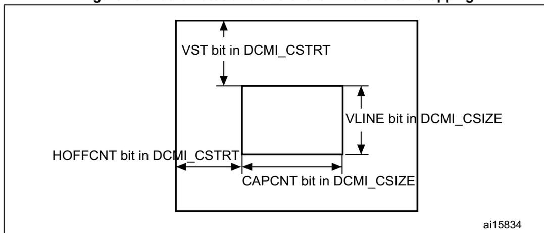
These registers specify the coordinates of the starting point of the capture window as a line number (in the frame, starting from 0) and a number of pixel clocks (on the line, starting from 0), and the size of the window as a line number and a number of pixel clocks. The CAPCNT value can only be a multiple of 4 (two least significant bits are forced to 0) to allow the correct transfer of data through the DMA.
If the VSYNC signal goes active before the number of lines is specified in the DCMI_CWSIZE register, then the capture stops and an IT_FRAME interrupt is generated when enabled.
Figure 79. Data capture waveforms
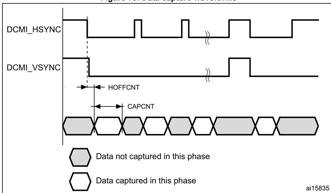
- 1. Here, the active state of DCMI_HSYNC and DCMI_VSYNC is 1.
- 2. DCMI_HSYNC and DCMI_VSYNC can change states at the same time.
15.5.6 JPEG format
To allow JPEG image reception, it is necessary to set the JPEG bit in the DCMI_CR register. JPEG images are not stored as lines and frames, so the VSYNC signal is used to start the capture while HSYNC serves as a data enable signal. The number of bytes in a line may not be a multiple of 4, you should therefore be careful when handling this case since a DMA request is generated each time a complete 32-bit word has been constructed from the captured data. When an end of frame is detected and the 32-bit word to be transferred has not been completely received, the remaining data are padded with '0s' and a DMA request is generated.
The crop feature and embedded synchronization codes cannot be used in the JPEG format.
15.5.7 FIFO
A four-word FIFO is implemented to manage data rate transfers on the AHB. The DCMI features a simple FIFO controller with a read pointer incremented each time the camera interface reads from the AHB, and a write pointer incremented each time the camera interface writes to the FIFO. There is no overrun protection to prevent the data from being overwritten if the AHB interface does not sustain the data transfer rate.
In case of overrun or errors in the synchronization signals, the FIFO is reset and the DCMI interface waits for a new start of frame.
15.6 Data format description
15.6.1 Data formats
Three types of data are supported:
- • 8-bit progressive video: either monochrome or raw Bayer format
- • YCbCr 4:2:2 progressive video
- • RGB565 progressive video. A pixel coded in 16 bits (5 bits for blue, 5 bits for red, 6 bits for green) takes two clock cycles to be transferred.
Compressed data: JPEG
For B&W, YCbCr or RGB data, the maximum input size is \( 2048 \times 2048 \) pixels. No limit in JPEG compressed mode.
For monochrome, RGB & YCbCr, the frame buffer is stored in raster mode. 32-bit words are used. Only the little endian format is supported.
Figure 80. Pixel raster scan order
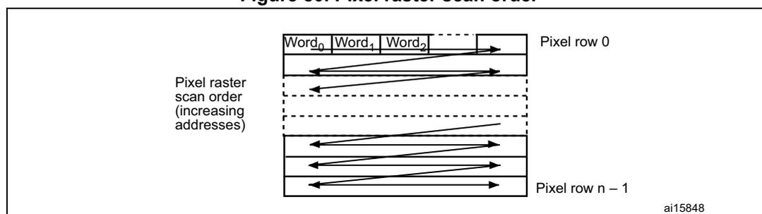
The diagram illustrates the pixel raster scan order. It shows a grid of pixels with arrows indicating the scan direction from left to right, top to bottom. The first row is labeled 'Pixel row 0' and the last row is labeled 'Pixel row n - 1'. Above the first row, three words are shown: Word 0 , Word 1 , and Word 2 . The text 'Pixel raster scan order (increasing addresses)' is on the left. The diagram is labeled ai15848.
15.6.2 Monochrome format
Characteristics:
- • Raster format
- • 8 bits per pixel
Table 84 shows how the data are stored.
Table 84. Data storage in monochrome progressive video format
| Byte address | 31:24 | 23:16 | 15:8 | 7:0 |
|---|---|---|---|---|
| 0 | n + 3 | n + 2 | n + 1 | n |
| 4 | n + 7 | n + 6 | n + 5 | n + 4 |
15.6.3 RGB format
Characteristics:
- • Raster format
- • RGB
- • Interleaved: one buffer: R, G & B interleaved: BRGBRGBRG, etc.
- • Optimized for display output
The RGB planar format is compatible with standard OS frame buffer display formats.
Only 16 BPP (bits per pixel): RGB565 (2 pixels per 32-bit word) is supported.
The 24 BPP (palletized format) and grayscale formats are not supported. Pixels are stored in a raster scan order, that is from top to bottom for pixel rows, and from left to right within a pixel row. Pixel components are R (red), G (green) and B (blue). All components have the same spatial resolution (4:4:4 format). A frame is stored in a single part, with the components interleaved on a pixel basis.
Table 85 shows how the data are stored.
Table 85. Data storage in RGB progressive video format
| Byte address | 31:27 | 26:21 | 20:16 | 15:11 | 10:5 | 4:0 |
|---|---|---|---|---|---|---|
| 0 | Red n + 1 | Green n + 1 | Blue n + 1 | Red n | Green n | Blue n |
| 4 | Red n + 4 | Green n + 3 | Blue n + 3 | Red n + 2 | Green n + 2 | Blue n + 2 |
15.6.4 YCbCr format
Characteristics:
- • Raster format
- • YCbCr 4:2:2
- • Interleaved: one Buffer: Y, Cb & Cr interleaved: CbYCrYCbYCr, etc.
Pixel components are Y (luminance or “luma”), Cb and Cr (chrominance or “chroma” blue and red). Each component is encoded in 8 bits. Luma and chroma are stored together (interleaved) as shown in Table 86 .
Table 86. Data storage in YCbCr progressive video format
| Byte address | 31:24 | 23:16 | 15:8 | 7:0 |
|---|---|---|---|---|
| 0 | Y n + 1 | Cr n | Y n | Cb n |
| 4 | Y n + 3 | Cr n + 2 | Y n + 2 | Cb n + 2 |
15.7 DCMI interrupts
Five interrupts are generated. All interrupts are maskable by software. The global interrupt (IT_DCMI) is the OR of all the individual interrupts. Table 87 gives the list of all interrupts.
Table 87. DCMI interrupts
| Interrupt name | Interrupt event |
|---|---|
| IT_LINE | Indicates the end of line |
| IT_FRAME | Indicates the end of frame capture |
| IT_OVR | indicates the overrun of data reception |
| IT_VSYNC | Indicates the synchronization frame |
| IT_ERR | Indicates the detection of an error in the embedded synchronization frame detection |
| IT_DCMI | Logic OR of the previous interrupts |
15.8 DCMI register description
All DCMI registers have to be accessed as 32-bit words, otherwise a bus error occurs.
15.8.1 DCMI control register 1 (DCMI_CR)
Address offset: 0x00
Reset value: 0x0000 0x0000
| 31 | 30 | 29 | 28 | 27 | 26 | 25 | 24 | 23 | 22 | 21 | 20 | 19 | 18 | 17 | 16 | 15 | 14 | 13 | 12 | 11 | 10 | 9 | 8 | 7 | 6 | 5 | 4 | 3 | 2 | 1 | 0 |
| Reserved | ENABLE | Reserved | EDM | FCRC | VSPOL | HSPOL | PCKPOL | ESS | JPEG | CROP | CM | CAPTURE | |||||||||||||||||||
| rw | rw | rw | rw | rw | rw | rw | rw | rw | rw | rw | rw | rw | |||||||||||||||||||
Bit 31:15 Reserved, must be kept at reset value.
Bit 14
ENABLE
: DCMI enable
0: DCMI disabled
1: DCMI enabled
Note: The DCMI configuration registers should be programmed correctly before enabling this Bit
Bit 13: 12 Reserved, must be kept at reset value.
Bits 11:10 EDM[1:0] : Extended data mode
- 00: Interface captures 8-bit data on every pixel clock
- 01: Interface captures 10-bit data on every pixel clock
- 10: Interface captures 12-bit data on every pixel clock
- 11: Interface captures 14-bit data on every pixel clock
Bits 9:8 FCRC[1:0] : Frame capture rate control
These bits define the frequency of frame capture. They are meaningful only in Continuous grab mode. They are ignored in snapshot mode.
- 00: All frames are captured
- 01: Every alternate frame captured (50% bandwidth reduction)
- 10: One frame in 4 frames captured (75% bandwidth reduction)
- 11: reserved
Bit 7 VSPOL : Vertical synchronization polarity
This bit indicates the level on the VSYNC pin when the data are not valid on the parallel interface.
- 0: VSYNC active low
- 1: VSYNC active high
Bit 6 HSPOL : Horizontal synchronization polarity
This bit indicates the level on the HSYNC pin when the data are not valid on the parallel interface.
- 0: HSYNC active low
- 1: HSYNC active high
Bit 5 PCKPOL : Pixel clock polarity
This bit configures the capture edge of the pixel clock
- 0: Falling edge active.
- 1: Rising edge active.
Bit 4 ESS : Embedded synchronization select
- 0: Hardware synchronization data capture (frame/line start/stop) is synchronized with the HSYNC/VSYNC signals.
- 1: Embedded synchronization data capture is synchronized with synchronization codes embedded in the data flow.
Note: Valid only for 8-bit parallel data. HSPOL/VSPOL are ignored when the ESS bit is set.
This bit is disabled in JPEG mode.
Bit 3 JPEG : JPEG format
- 0: Uncompressed video format
- 1: This bit is used for JPEG data transfers. The HSYNC signal is used as data enable. The crop and embedded synchronization features (ESS bit) cannot be used in this mode.
Bits 2 CROP : Crop feature
- 0: The full image is captured. In this case the total number of bytes in an image frame should be a multiple of 4
- 1: Only the data inside the window specified by the crop register are captured. If the size of the crop window exceeds the picture size, then only the picture size is captured.
0: Continuous grab mode - The received data are transferred into the destination memory through the DMA. The buffer location and mode (linear or circular buffer) is controlled through the system DMA.
1: Snapshot mode (single frame) - Once activated, the interface waits for the start of frame and then transfers a single frame through the DMA. At the end of the frame, the CAPTURE bit is automatically reset.
Bit 0 CAPTURE : Capture enable0: Capture disabled.
1: Capture enabled.
The camera interface waits for the first start of frame, then a DMA request is generated to transfer the received data into the destination memory.
In snapshot mode, the CAPTURE bit is automatically cleared at the end of the 1st frame received.
In continuous grab mode, if the software clears this bit while a capture is ongoing, the bit is effectively cleared after the frame end.
Note: The DMA controller and all DCMI configuration registers should be programmed correctly before enabling this bit.
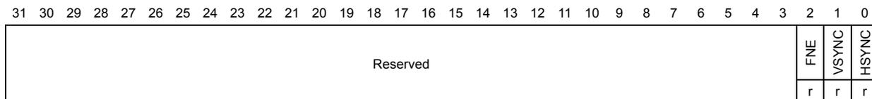
15.8.2 DCMI status register (DCMI_SR)
Address offset: 0x04
Reset value: 0x0000 0x0000
| 31 | 30 | 29 | 28 | 27 | 26 | 25 | 24 | 23 | 22 | 21 | 20 | 19 | 18 | 17 | 16 | 15 | 14 | 13 | 12 | 11 | 10 | 9 | 8 | 7 | 6 | 5 | 4 | 3 | 2 | 1 | 0 |
| Reserved | FNE | VSYNC | HSYNC | ||||||||||||||||||||||||||||
| r | r | r | |||||||||||||||||||||||||||||
Bits 31:3 Reserved, must be kept at reset value.
- Bit 2
FNE
: FIFO not empty
- This bit gives the status of the FIFO
- 1: FIFO contains valid data
- 0: FIFO empty
- Bit 1
VSYNC
- This bit gives the state of the VSYNC pin with the correct programmed polarity.
- When embedded synchronization codes are used, the meaning of this bit is the following:
- 0: active frame
- 1: synchronization between frames
- In case of embedded synchronization, this bit is meaningful only if the CAPTURE bit in DCMI_CR is set.
- Bit 0
HSYNC
- This bit gives the state of the HSYNC pin with the correct programmed polarity.
- When embedded synchronization codes are used, the meaning of this bit is the following:
- 0: active line
- 1: synchronization between lines
- In case of embedded synchronization, this bit is meaningful only if the CAPTURE bit in DCMI_CR is set.
15.8.3 DCMI raw interrupt status register (DCMI_RIS)
Address offset: 0x08
Reset value: 0x0000 0x0000
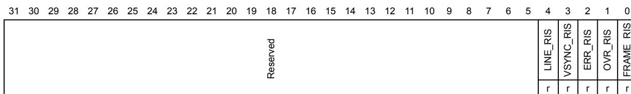
| 31 | 30 | 29 | 28 | 27 | 26 | 25 | 24 | 23 | 22 | 21 | 20 | 19 | 18 | 17 | 16 | 15 | 14 | 13 | 12 | 11 | 10 | 9 | 8 | 7 | 6 | 5 | 4 | 3 | 2 | 1 | 0 | |
| Reserved | LINE_RIS | VSYNC_RIS | ERR_RIS | OVR_RIS | FRAME_RIS | |||||||||||||||||||||||||||
| r | r | r | r | r | ||||||||||||||||||||||||||||
DCMI_RIS gives the raw interrupt status and is accessible in read only. When read, this register returns the status of the corresponding interrupt before masking with the DCMI_IER register value.
Bits 31:5 Reserved, must be kept at reset value.
Bit 4 LINE_RIS : Line raw interrupt status
This bit gets set when the HSYNC signal changes from the inactive state to the active state. It goes high even if the line is not valid.
In the case of embedded synchronization, this bit is set only if the CAPTURE bit in DCMI_CR is set.
It is cleared by writing a '1' to the LINE_ISC bit in DCMI_ICR.
Bit 3 VSYNC_RIS : VSYNC raw interrupt status
This bit is set when the VSYNC signal changes from the inactive state to the active state.
In the case of embedded synchronization, this bit is set only if the CAPTURE bit is set in DCMI_CR.
It is cleared by writing a '1' to the VSYNC_ISC bit in DCMI_ICR.
Bit 2 ERR_RIS : Synchronization error raw interrupt status
0: No synchronization error detected
1: Embedded synchronization characters are not received in the correct order.
This bit is valid only in the embedded synchronization mode. It is cleared by writing a '1' to the ERR_ISC bit in DCMI_ICR.
Note: This bit is available only in embedded synchronization mode.
Bit 1 OVR_RIS : Overrun raw interrupt status
0: No data buffer overrun occurred
1: A data buffer overrun occurred and the data FIFO is corrupted.
This bit is cleared by writing a '1' to the OVR_ISC bit in DCMI_ICR.
Bit 0 FRAME_RIS : Capture complete raw interrupt status
0: No new capture
1: A frame has been captured.
This bit is set when a frame or window has been captured.
In case of a cropped window, this bit is set at the end of line of the last line in the crop. It is set even if the captured frame is empty (e.g. window cropped outside the frame).
This bit is cleared by writing a '1' to the FRAME_ISC bit in DCMI_ICR.
15.8.4 DCMI interrupt enable register (DCMI_IER)
Address offset: 0x0C
Reset value: 0x0000 0x0000
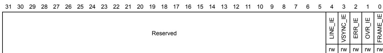
| 31 | 30 | 29 | 28 | 27 | 26 | 25 | 24 | 23 | 22 | 21 | 20 | 19 | 18 | 17 | 16 | 15 | 14 | 13 | 12 | 11 | 10 | 9 | 8 | 7 | 6 | 5 | 4 | 3 | 2 | 1 | 0 | |
| Reserved | LINE_IE | VSYNC_IE | ERR_IE | OVR_IE | FRAME_IE | |||||||||||||||||||||||||||
| rw | rw | rw | rw | rw | ||||||||||||||||||||||||||||
The DCMI_IER register is used to enable interrupts. When one of the DCMI_IER bits is set, the corresponding interrupt is enabled. This register is accessible in both read and write.
Bits 31:5 Reserved, must be kept at reset value.
Bit 4 LINE_IE : Line interrupt enable
0: No interrupt generation when the line is received
1: An Interrupt is generated when a line has been completely received
Bit 3 VSYNC_IE : VSYNC interrupt enable
0: No interrupt generation
1: An interrupt is generated on each VSYNC transition from the inactive to the active state
The active state of the VSYNC signal is defined by the VSPOL bit.
Bit 2 ERR_IE : Synchronization error interrupt enable
0: No interrupt generation
1: An interrupt is generated if the embedded synchronization codes are not received in the correct order.
Note: This bit is available only in embedded synchronization mode.
Bit 1 OVR_IE : Overrun interrupt enable
0: No interrupt generation
1: An interrupt is generated if the DMA was not able to transfer the last data before new data (32-bit) are received.
Bit 0 FRAME_IE : Capture complete interrupt enable
0: No interrupt generation
1: An interrupt is generated at the end of each received frame/crop window (in crop mode).
15.8.5 DCMI masked interrupt status register (DCMI_MIS)
This DCMI_MIS register is a read-only register. When read, it returns the current masked status value (depending on the value in DCMI_IER) of the corresponding interrupt. A bit in this register is set if the corresponding enable bit in DCMI_IER is set and the corresponding bit in DCMI_RIS is set.
Address offset: 0x10
Reset value: 0x0000
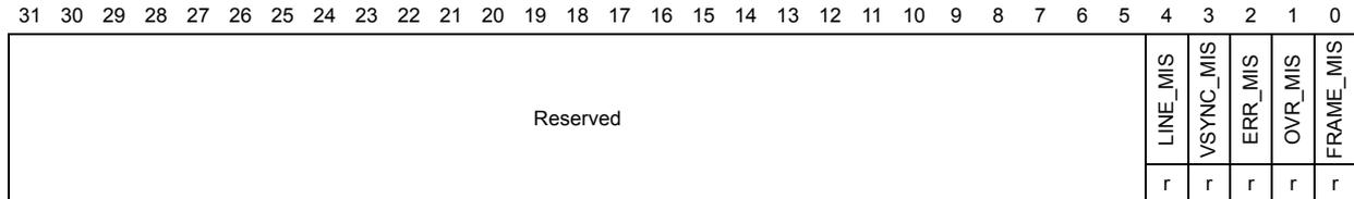
| 31 | 30 | 29 | 28 | 27 | 26 | 25 | 24 | 23 | 22 | 21 | 20 | 19 | 18 | 17 | 16 | 15 | 14 | 13 | 12 | 11 | 10 | 9 | 8 | 7 | 6 | 5 | 4 | 3 | 2 | 1 | 0 |
| Reserved | LINE_MIS | VSYNC_MIS | ERR_MIS | OVR_MIS | FRAME_MIS | ||||||||||||||||||||||||||
| r | r | r | r | r | |||||||||||||||||||||||||||
Bits 31:5 Reserved , must be kept at reset value.
Bit 4 LINE_MIS : Line masked interrupt status
This bit gives the status of the masked line interrupt
0: No interrupt generation when the line is received
1: An Interrupt is generated when a line has been completely received and the LINE_IE bit is set in DCMI_IER.
Bit 3 VSYNC_MIS : VSYNC masked interrupt status
This bit gives the status of the masked VSYNC interrupt
0: No interrupt is generated on VSYNC transitions
1: An interrupt is generated on each VSYNC transition from the inactive to the active state and the VSYNC_IE bit is set in DCMI_IER.
The active state of the VSYNC signal is defined by the VSPOL bit.
Bit 2 ERR_MIS : Synchronization error masked interrupt status
This bit gives the status of the masked synchronization error interrupt
0: No interrupt is generated on a synchronization error
1: An interrupt is generated if the embedded synchronization codes are not received in the correct order and the ERR_IE bit in DCMI_IER is set.
Note: This bit is available only in embedded synchronization mode.
Bit 1 OVR_MIS : Overrun masked interrupt status
This bit gives the status of the masked overflow interrupt
0: No interrupt is generated on overrun
1: An interrupt is generated if the DMA was not able to transfer the last data before new data (32-bit) are received and the OVR_IE bit is set in DCMI_IER.
Bit 0 FRAME_MIS : Capture complete masked interrupt status
This bit gives the status of the masked capture complete interrupt
0: No interrupt is generated after a complete capture
1: An interrupt is generated at the end of each received frame/crop window (in crop mode) and the FRAME_IE bit is set in DCMI_IER.
15.8.6 DCMI interrupt clear register (DCMI_ICR)
Address offset: 0x14
Reset value: 0x0000 0x0000
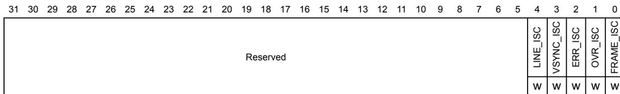
| 31 | 30 | 29 | 28 | 27 | 26 | 25 | 24 | 23 | 22 | 21 | 20 | 19 | 18 | 17 | 16 | 15 | 14 | 13 | 12 | 11 | 10 | 9 | 8 | 7 | 6 | 5 | 4 | 3 | 2 | 1 | 0 | |
| Reserved | LINE_ISC | VSYNC_ISC | ERR_ISC | OVR_ISC | FRAME_ISC | |||||||||||||||||||||||||||
| W | W | W | W | W | ||||||||||||||||||||||||||||
The DCMI_ICR register is write-only. Writing a '1' into a bit of this register clears the corresponding bit in the DCMI_RIS and DCMI_MIS registers. Writing a '0' has no effect.
Bits 15:5 Reserved, must be kept at reset value.
Bit 4 LINE_ISC : line interrupt status clear
Writing a '1' into this bit clears LINE_RIS in the DCMI_RIS register
Bit 3 VSYNC_ISC : Vertical synch interrupt status clear
Writing a '1' into this bit clears the VSYNC_RIS bit in DCMI_RIS
Bit 2 ERR_ISC : Synchronization error interrupt status clear
Writing a '1' into this bit clears the ERR_RIS bit in DCMI_RIS
Note: This bit is available only in embedded synchronization mode.
Bit 1 OVR_ISC : Overrun interrupt status clear
Writing a '1' into this bit clears the OVR_RIS bit in DCMI_RIS
Bits 0 FRAME_ISC : Capture complete interrupt status clear
Writing a '1' into this bit clears the FRAME_RIS bit in DCMI_RIS
15.8.7 DCMI embedded synchronization code register (DCMI_ESCR)
Address offset: 0x18
Reset value: 0x0000 0x0000
| 31 | 30 | 29 | 28 | 27 | 26 | 25 | 24 | 23 | 22 | 21 | 20 | 19 | 18 | 17 | 16 | 15 | 14 | 13 | 12 | 11 | 10 | 9 | 8 | 7 | 6 | 5 | 4 | 3 | 2 | 1 | 0 |
|---|---|---|---|---|---|---|---|---|---|---|---|---|---|---|---|---|---|---|---|---|---|---|---|---|---|---|---|---|---|---|---|
| FEC | LEC | LSC | FSC | ||||||||||||||||||||||||||||
| rw | rw | rw | rw | rw | rw | rw | rw | rw | rw | rw | rw | rw | rw | rw | rw | rw | rw | rw | rw | rw | rw | rw | rw | rw | rw | rw | rw | rw | rw | rw | rw |
Bits 31:24 FEC : Frame end delimiter code
This byte specifies the code of the frame end delimiter. The code consists of 4 bytes in the form of 0xFF, 0x00, 0x00, FEC.
If FEC is programmed to 0xFF, all the unused codes (0xFF0000XY) are interpreted as frame end delimiters.
Bits 23:16 LEC : Line end delimiter code
This byte specifies the code of the line end delimiter. The code consists of 4 bytes in the form of 0xFF, 0x00, 0x00, LEC.
Bits 15:8 LSC : Line start delimiter code
This byte specifies the code of the line start delimiter. The code consists of 4 bytes in the form of 0xFF, 0x00, 0x00, LSC.
Bits 7:0 FSC : Frame start delimiter code
This byte specifies the code of the frame start delimiter. The code consists of 4 bytes in the form of 0xFF, 0x00, 0x00, FSC.
If FSC is programmed to 0xFF, no frame start delimiter is detected. But, the 1 st occurrence of LSC after an FEC code is interpreted as a start of frame delimiter.
15.8.8 DCMI embedded synchronization unmask register (DCMI_ESUR)
Address offset: 0x1C
Reset value: 0x0000 0x0000
| 31 | 30 | 29 | 28 | 27 | 26 | 25 | 24 | 23 | 22 | 21 | 20 | 19 | 18 | 17 | 16 | 15 | 14 | 13 | 12 | 11 | 10 | 9 | 8 | 7 | 6 | 5 | 4 | 3 | 2 | 1 | 0 |
|---|---|---|---|---|---|---|---|---|---|---|---|---|---|---|---|---|---|---|---|---|---|---|---|---|---|---|---|---|---|---|---|
| FEU | LEU | LSU | FSU | ||||||||||||||||||||||||||||
| rw | rw | rw | rw | rw | rw | rw | rw | rw | rw | rw | rw | rw | rw | rw | rw | rw | rw | rw | rw | rw | rw | rw | rw | rw | rw | rw | rw | rw | rw | rw | rw |
Bits 31:24 FEU: Frame end delimiter unmask
This byte specifies the mask to be applied to the code of the frame end delimiter.
0: The corresponding bit in the FEC byte in DCMI_ESCR is masked while comparing the frame end delimiter with the received data.
1: The corresponding bit in the FEC byte in DCMI_ESCR is compared while comparing the frame end delimiter with the received data
Bits 23:16 LEU: Line end delimiter unmask
This byte specifies the mask to be applied to the code of the line end delimiter.
0: The corresponding bit in the LEC byte in DCMI_ESCR is masked while comparing the line end delimiter with the received data
1: The corresponding bit in the LEC byte in DCMI_ESCR is compared while comparing the line end delimiter with the received data
Bits 15:8 LSU: Line start delimiter unmask
This byte specifies the mask to be applied to the code of the line start delimiter.
0: The corresponding bit in the LSC byte in DCMI_ESCR is masked while comparing the line start delimiter with the received data
1: The corresponding bit in the LSC byte in DCMI_ESCR is compared while comparing the line start delimiter with the received data
Bits 7:0 FSU: Frame start delimiter unmask
This byte specifies the mask to be applied to the code of the frame start delimiter.
0: The corresponding bit in the FSC byte in DCMI_ESCR is masked while comparing the frame start delimiter with the received data
1: The corresponding bit in the FSC byte in DCMI_ESCR is compared while comparing the frame start delimiter with the received data
15.8.9 DCMI crop window start (DCMI_CWSTRT)
Address offset: 0x20
Reset value: 0x0000 0x0000

| 31 | 30 | 29 | 28 | 27 | 26 | 25 | 24 | 23 | 22 | 21 | 20 | 19 | 18 | 17 | 16 | 15 | 14 | 13 | 12 | 11 | 10 | 9 | 8 | 7 | 6 | 5 | 4 | 3 | 2 | 1 | 0 |
| Reserved | VST[12:0] | Reserved | HOFFCNT[13:0] | ||||||||||||||||||||||||||||
| rw | rw | rw | rw | rw | rw | rw | rw | rw | rw | rw | rw | rw | rw | rw | rw | rw | rw | rw | rw | rw | rw | rw | rw | rw | rw | rw | |||||
Bits 31:29 Reserved, must be kept at reset value.
Bits 28:16
VST[12:0]
: Vertical start line count
The image capture starts with this line number. Previous line data are ignored.
0x0000 => line 1
0x0001 => line 2
0x0002 => line 3
....
Bits 15:14 Reserved, must be kept at reset value.
Bit 13:0
HOFFCNT[13:0]
: Horizontal offset count
This value gives the number of pixel clocks to count before starting a capture.
15.8.10 DCMI crop window size (DCMI_CWSIZE)
Address offset: 0x24
Reset value: 0x0000 0x0000

| 31 | 30 | 29 | 28 | 27 | 26 | 25 | 24 | 23 | 22 | 21 | 20 | 19 | 18 | 17 | 16 | 15 | 14 | 13 | 12 | 11 | 10 | 9 | 8 | 7 | 6 | 5 | 4 | 3 | 2 | 1 | 0 |
| Reserved | VLINE[13:0] | Reserved | CAPCNT[13:0] | ||||||||||||||||||||||||||||
| rw | rw | rw | rw | rw | rw | rw | rw | rw | rw | rw | rw | rw | rw | rw | rw | rw | rw | rw | rw | rw | rw | rw | rw | rw | rw | rw | rw | ||||
Bits 31:30 Reserved, must be kept at reset value.
Bitst 29:16
VLINE[13:0]
: Vertical line count
This value gives the number of lines to be captured from the starting point.
0x0000 => 1 line
0x0001 => 2 lines
0x0002 => 3 lines
....
Bits 15:14 Reserved, must be kept at reset value.
Bits 13:0
CAPCNT[13:0]
: Capture count
This value gives the number of pixel clocks to be captured from the starting point on the same line. It value should corresponds to word-aligned data for different widths of parallel interfaces.
0x0000 => 1 pixel
0x0001 => 2 pixels
0x0002 => 3 pixels
....
15.8.11 DCMI data register (DCMI_DR)
Address offset: 0x28
Reset value: 0x0000 0x0000
| 31 | 30 | 29 | 28 | 27 | 26 | 25 | 24 | 23 | 22 | 21 | 20 | 19 | 18 | 17 | 16 | 15 | 14 | 13 | 12 | 11 | 10 | 9 | 8 | 7 | 6 | 5 | 4 | 3 | 2 | 1 | 0 |
|---|---|---|---|---|---|---|---|---|---|---|---|---|---|---|---|---|---|---|---|---|---|---|---|---|---|---|---|---|---|---|---|
| Byte3 | Byte2 | Byte1 | Byte0 | ||||||||||||||||||||||||||||
| r | r | r | r | r | r | r | r | r | r | r | r | r | r | r | r | r | r | r | r | r | r | r | r | r | r | r | r | r | r | r | r |
Bits 31:24 Data byte 3
Bits 23:16 Data byte 2
Bits 15:8 Data byte 1
Bits 7:0 Data byte 0
The digital camera Interface packages all the received data in 32-bit format before requesting a DMA transfer. A 4-word deep FIFO is available to leave enough time for DMA transfers and avoid DMA overrun conditions.
15.8.12 DCMI register map
Table 88 summarizes the DCMI registers.
Table 88. DCMI register map and reset values
| Offset | Register | 31 | 30 | 29 | 28 | 27 | 26 | 25 | 24 | 23 | 22 | 21 | 20 | 19 | 18 | 17 | 16 | 15 | 14 | 13 | 12 | 11 | 10 | 9 | 8 | 7 | 6 | 5 | 4 | 3 | 2 | 1 | 0 |
|---|---|---|---|---|---|---|---|---|---|---|---|---|---|---|---|---|---|---|---|---|---|---|---|---|---|---|---|---|---|---|---|---|---|
| 0x00 | DCMI_CR | Reserved | ENABLE | Reserved | EDM | Reserved | FCRC | VSPOL | HSPOL | PCKPOL | ESS | JPEG | CROP | CM | Reserved | CAPTURE | |||||||||||||||||
| Reset value | 0 | 0 | 0 | 0 | 0 | 0 | 0 | 0 | 0 | 0 | 0 | 0 | |||||||||||||||||||||
| 0x04 | DCMI_SR | Reserved | FNE | Reserved | VSYNC | HSYNC | Reserved | ||||||||||||||||||||||||||
| Reset value | 0 | 0 | 0 | ||||||||||||||||||||||||||||||
| 0x08 | DCMI_RIS | Reserved | LINE_RIS | VSYNC_RIS | ERR_RIS | OVR_RIS | FRAME_RIS | ||||||||||||||||||||||||||
| Reset value | 0 | 0 | 0 | 0 | 0 | ||||||||||||||||||||||||||||
| 0x0C | DCMI_IER | Reserved | LINE_IE | VSYNC_IE | ERR_IE | OVR_IE | FRAME_IE | ||||||||||||||||||||||||||
| Reset value | 0 | 0 | 0 | 0 | 0 | ||||||||||||||||||||||||||||
| 0x10 | DCMI_MIS | Reserved | LINE_MIS | VSYNC_MIS | ERR_MIS | OVR_MIS | FRAME_MIS | ||||||||||||||||||||||||||
| Reset value | 0 | 0 | 0 | 0 | 0 | ||||||||||||||||||||||||||||
Table 88. DCMI register map and reset values (continued)
| Offset | Register | 31 | 30 | 29 | 28 | 27 | 26 | 25 | 24 | 23 | 22 | 21 | 20 | 19 | 18 | 17 | 16 | 15 | 14 | 13 | 12 | 11 | 10 | 9 | 8 | 7 | 6 | 5 | 4 | 3 | 2 | 1 | 0 |
|---|---|---|---|---|---|---|---|---|---|---|---|---|---|---|---|---|---|---|---|---|---|---|---|---|---|---|---|---|---|---|---|---|---|
| 0x14 | DCMI_ICR | Reserved | LINE_ISC | VSYNC_ISC | ERR_ISC | OVR_ISC | FRAME_ISC | ||||||||||||||||||||||||||
| Reset value | 0 | 0 | 0 | 0 | 0 | ||||||||||||||||||||||||||||
| 0x18 | DCMI_ESCR | FEC | LEC | LSC | FSC | ||||||||||||||||||||||||||||
| Reset value | 0 | 0 | 0 | 0 | 0 | 0 | 0 | 0 | 0 | 0 | 0 | 0 | 0 | 0 | 0 | 0 | 0 | 0 | 0 | 0 | 0 | 0 | 0 | 0 | 0 | 0 | 0 | 0 | 0 | 0 | 0 | 0 | |
| 0x1C | DCMI_ESUR | FEU | LEU | LSU | FSU | ||||||||||||||||||||||||||||
| Reset value | 0 | 0 | 0 | 0 | 0 | 0 | 0 | 0 | 0 | 0 | 0 | 0 | 0 | 0 | 0 | 0 | 0 | 0 | 0 | 0 | 0 | 0 | 0 | 0 | 0 | 0 | 0 | 0 | 0 | 0 | 0 | 0 | |
| 0x20 | DCMI_CWSTR T | Reserved | VST[12:0] | ||||||||||||||||||||||||||||||
| Reset value | 0 | 0 | 0 | 0 | 0 | 0 | 0 | 0 | 0 | 0 | 0 | 0 | 0 | 0 | 0 | 0 | 0 | 0 | 0 | 0 | 0 | 0 | 0 | 0 | 0 | 0 | 0 | 0 | 0 | 0 | 0 | ||
| 0x24 | DCMI_CWSIZ E | Reserved | VLINE[13:0] | ||||||||||||||||||||||||||||||
| Reset value | 0 | 0 | 0 | 0 | 0 | 0 | 0 | 0 | 0 | 0 | 0 | 0 | 0 | 0 | 0 | 0 | 0 | 0 | 0 | 0 | 0 | 0 | 0 | 0 | 0 | 0 | 0 | 0 | 0 | 0 | 0 | ||
| 0x28 | DCMI_DR | Byte3 | Byte2 | Byte1 | Byte0 | ||||||||||||||||||||||||||||
| Reset value | 0 | 0 | 0 | 0 | 0 | 0 | 0 | 0 | 0 | 0 | 0 | 0 | 0 | 0 | 0 | 0 | 0 | 0 | 0 | 0 | 0 | 0 | 0 | 0 | 0 | 0 | 0 | 0 | 0 | 0 | 0 | 0 | |
Refer to Section 2.3: Memory map for the register boundary addresses.