13. Analog-to-digital converter (ADC)
This section applies to the whole STM32F4xx family, unless otherwise specified.
13.1 ADC introduction
The 12-bit ADC is a successive approximation analog-to-digital converter. It has up to 19 multiplexed channels allowing it to measure signals from 16 external sources, two internal sources, and the \( V_{BAT} \) channel. The A/D conversion of the channels can be performed in single, continuous, scan or discontinuous mode. The result of the ADC is stored into a left- or right-aligned 16-bit data register.
The analog watchdog feature allows the application to detect if the input voltage goes beyond the user-defined, higher or lower thresholds.
13.2 ADC main features
- • 12-bit, 10-bit, 8-bit or 6-bit configurable resolution
- • Interrupt generation at the end of conversion, end of injected conversion, and in case of analog watchdog or overrun events
- • Single and continuous conversion modes
- • Scan mode for automatic conversion of channel 0 to channel 'n'
- • Data alignment with in-built data coherency
- • Channel-wise programmable sampling time
- • External trigger option with configurable polarity for both regular and injected conversions
- • Discontinuous mode
- • Dual/Triple mode (on devices with 2 ADCs or more)
- • Configurable DMA data storage in Dual/Triple ADC mode
- • Configurable delay between conversions in Dual/Triple interleaved mode
- • ADC conversion type (refer to the datasheets)
- • ADC supply requirements: 2.4 V to 3.6 V at full speed and down to 1.8 V at slower speed
- • ADC input range: \( V_{REF-} \leq V_{IN} \leq V_{REF+} \)
- • DMA request generation during regular channel conversion
Figure 44 shows the block diagram of the ADC.
Note: \( V_{REF-} \) , if available (depending on package), must be tied to \( V_{SSA} \) .
13.3 ADC functional description
Figure 44 shows a single ADC block diagram and Table 66 gives the ADC pin description.
Figure 44. Single ADC block diagram
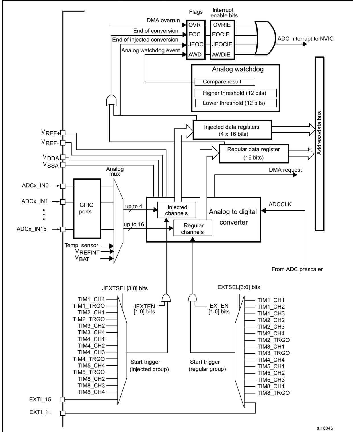
The diagram illustrates the internal architecture of the ADC. On the left, input pins include VREF+, VREF-, VDDA, VSSA, ADCx_IN0 through ADCx_IN15, Temp. sensor, VREFINT, and VBAT. These connect to an Analog mux which feeds into the ADC core. The core contains 'Injected channels' (up to 4) and 'Regular channels' (up to 16), which are processed by an 'Analog to digital converter'. The converter is controlled by 'JEXTSEL[3:0] bits' and 'EXTSEL[3:0] bits' for start triggers, and 'JEXTEN[1:0] bits' and 'EXTEN[1:0] bits'. External triggers come from TIM1_CH4, TIM1_TRGO, TIM2_CH1, TIM2_TRGO, TIM3_CH2, TIM3_CH4, TIM4_CH1, TIM4_CH2, TIM4_CH3, TIM4_TRGO, TIM5_CH4, TIM5_TRGO, TIM8_CH2, TIM8_CH3, TIM8_CH4, EXTI_15, and EXTI_11. The converter outputs data to 'Injected data registers (4 x 16 bits)' and a 'Regular data register (16 bits)'. These registers connect to an 'Address/data bus' and generate 'DMA request' signals. Above the registers, a logic block generates 'Flags' (DMA overrun, End of conversion, End of injected conversion, Analog watchdog event) and 'Interrupt enable bits' (OVR, EOC, JEOC, AWD, OVRIE, EOCIE, JEOCIE, AWDIE). These are combined via an OR gate to produce an 'ADC Interrupt to NVIC'. An 'Analog watchdog' block contains 'Compare result', 'Higher threshold (12 bits)', and 'Lower threshold (12 bits)'. The 'ADCCLK' input is derived 'From ADC prescaler'. A reference number 'ai16046' is in the bottom right corner.
Table 66. ADC pins
| Name | Signal type | Remarks |
|---|---|---|
| V REF+ | Input, analog reference positive | The higher/positive reference voltage for the ADC, \( 1.8\text{ V} \leq V_{\text{REF+}} \leq V_{\text{DDA}} \) |
| V DDA | Input, analog supply | Analog power supply equal to V
DD
and
\(
2.4\text{ V} \leq V_{\text{DDA}} \leq V_{\text{DD}}\ (3.6\text{ V})
\)
for full speed \( 1.8\text{ V} \leq V_{\text{DDA}} \leq V_{\text{DD}}\ (3.6\text{ V}) \) for reduced speed |
| V REF- | Input, analog reference negative | The lower/negative reference voltage for the ADC, \( V_{\text{REF-}} = V_{\text{SSA}} \) |
| V SSA | Input, analog supply ground | Ground for analog power supply equal to V SS |
| ADCx_IN[15:0] | Analog input signals | 16 analog input channels |
13.3.1 ADC on-off control
The ADC is powered on by setting the ADON bit in the ADC_CR2 register. When the ADON bit is set for the first time, it wakes up the ADC from the Power-down mode.
Conversion starts when either the SWSTART or the JSWSTART bit is set.
You can stop conversion and put the ADC in power down mode by clearing the ADON bit. In this mode the ADC consumes almost no power (only a few µA).
13.3.2 ADC clock
The ADC features two clock schemes:
- • Clock for the analog circuitry: ADCCLK, common to all ADCs
This clock is generated from the APB2 clock divided by a programmable prescaler that allows the ADC to work at \( f_{\text{PCLK2}}/2, /4, /6 \) or \( /8 \) . Refer to the datasheets for the maximum value of ADCCLK. - • Clock for the digital interface (used for registers read/write access)
This clock is equal to the APB2 clock. The digital interface clock can be enabled/disabled individually for each ADC through the RCC APB2 peripheral clock enable register (RCC_APB2ENR).
13.3.3 Channel selection
There are 16 multiplexed channels. It is possible to organize the conversions in two groups: regular and injected. A group consists of a sequence of conversions that can be done on any channel and in any order. For instance, it is possible to implement the conversion sequence in the following order: ADC_IN3, ADC_IN8, ADC_IN2, ADC_IN2, ADC_IN0, ADC_IN2, ADC_IN2, ADC_IN15.
- • A regular group is composed of up to 16 conversions. The regular channels and their order in the conversion sequence must be selected in the ADC_SQRx registers. The total number of conversions in the regular group must be written in the L[3:0] bits in the ADC_SQR1 register.
- • An injected group is composed of up to 4 conversions. The injected channels and their order in the conversion sequence must be selected in the ADC_JSQR register.
The total number of conversions in the injected group must be written in the L[1:0] bits in the ADC_JSQR register.
If the ADC_SQRx or ADC_JSQR registers are modified during a conversion, the current conversion is reset and a new start pulse is sent to the ADC to convert the newly chosen group.
Temperature sensor, V REFINT and V BAT internal channels
- • For the STM32F40x and STM32F41x devices, the temperature sensor is internally connected to channel ADC1_IN16.
The internal reference voltage VREFINT is connected to ADC1_IN17.
- • For the STM32F42x and STM32F43x devices, the temperature sensor is internally connected to ADC1_IN18 channel which is shared with VBAT. Only one conversion, temperature sensor or VBAT, must be selected at a time. When the temperature sensor and VBAT conversion are set simultaneously, only the VBAT conversion is performed.
The internal reference voltage VREFINT is connected to ADC1_IN17.
The V BAT channel (connected to channel ADC1_IN18) can also be converted as an injected or regular channel.
Note: The temperature sensor, V REFINT and the V BAT channel are available only on the master ADC1 peripheral.
13.3.4 Single conversion mode
In Single conversion mode the ADC does one conversion. This mode is started with the CONT bit at 0 by either:
- • setting the SWSTART bit in the ADC_CR2 register (for a regular channel only)
- • setting the JSWSTART bit (for an injected channel)
- • external trigger (for a regular or injected channel)
Once the conversion of the selected channel is complete:
- • If a regular channel was converted:
- – The converted data are stored into the 16-bit ADC_DR register
- – The EOC (end of conversion) flag is set
- – An interrupt is generated if the EOCIE bit is set
- • If an injected channel was converted:
- – The converted data are stored into the 16-bit ADC_JDR1 register
- – The JEOC (end of conversion injected) flag is set
- – An interrupt is generated if the JEOCIE bit is set
Then the ADC stops.
13.3.5 Continuous conversion mode
In continuous conversion mode, the ADC starts a new conversion as soon as it finishes one. This mode is started with the CONT bit at 1 either by external trigger or by setting the SWSTART bit in the ADC_CR2 register (for regular channels only).
After each conversion:
- • If a regular group of channels was converted:
- – The last converted data are stored into the 16-bit ADC_DR register
- – The EOC (end of conversion) flag is set
- – An interrupt is generated if the EOCIE bit is set
Note: Injected channels cannot be converted continuously. The only exception is when an injected channel is configured to be converted automatically after regular channels in continuous mode (using JAUTO bit), refer to Auto-injection section ).
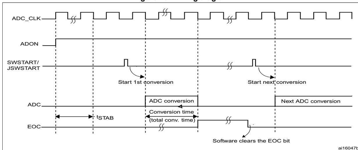
13.3.6 Timing diagram
As shown in Figure 45 , the ADC needs a stabilization time of \( t_{STAB} \) before it starts converting accurately. After the start of the ADC conversion and after 15 clock cycles, the EOC flag is set and the 16-bit ADC data register contains the result of the conversion.
Figure 45. Timing diagram
13.3.7 Analog watchdog
The AWD analog watchdog status bit is set if the analog voltage converted by the ADC is below a lower threshold or above a higher threshold. These thresholds are programmed in the 12 least significant bits of the ADC_HTR and ADC_LTR 16-bit registers. An interrupt can be enabled by using the AWDIE bit in the ADC_CR1 register.
The threshold value is independent of the alignment selected by the ALIGN bit in the ADC_CR2 register. The analog voltage is compared to the lower and higher thresholds before alignment.
Table 67 shows how the ADC_CR1 register should be configured to enable the analog watchdog on one or more channels.
Figure 46. Analog watchdog's guarded area

Table 67. Analog watchdog channel selection
| Channels guarded by the analog watchdog | ADC_CR1 register control bits (x = don't care) | ||
|---|---|---|---|
| AWDSGL bit | AWDEN bit | JAWDEN bit | |
| None | x | 0 | 0 |
| All injected channels | 0 | 0 | 1 |
| All regular channels | 0 | 1 | 0 |
| All regular and injected channels | 0 | 1 | 1 |
| Single (1) injected channel | 1 | 0 | 1 |
| Single (1) regular channel | 1 | 1 | 0 |
| Single (1) regular or injected channel | 1 | 1 | 1 |
1. Selected by the AWDCH[4:0] bits
13.3.8 Scan mode
This mode is used to scan a group of analog channels.
The Scan mode is selected by setting the SCAN bit in the ADC_CR1 register. Once this bit has been set, the ADC scans all the channels selected in the ADC_SQRx registers (for regular channels) or in the ADC_JSQR register (for injected channels). A single conversion is performed for each channel of the group. After each end of conversion, the next channel in the group is converted automatically. If the CONT bit is set, regular channel conversion does not stop at the last selected channel in the group but continues again from the first selected channel.
If the DMA bit is set, the direct memory access (DMA) controller is used to transfer the data converted from the regular group of channels (stored in the ADC_DR register) to SRAM after each regular channel conversion.
The EOC bit is set in the ADC_SR register:
- • At the end of each regular group sequence if the EOCS bit is cleared to 0
- • At the end of each regular channel conversion if the EOCS bit is set to 1
The data converted from an injected channel are always stored into the ADC_JDRx registers.
13.3.9 Injected channel management
Triggered injection
To use triggered injection, the JAUTO bit must be cleared in the ADC_CR1 register.
- 1. Start the conversion of a group of regular channels either by external trigger or by setting the SWSTART bit in the ADC_CR2 register.
- 2. If an external injected trigger occurs or if the JSWSTART bit is set during the conversion of a regular group of channels, the current conversion is reset and the injected channel sequence switches to Scan-once mode.
- 3. Then, the regular conversion of the regular group of channels is resumed from the last interrupted regular conversion.
If a regular event occurs during an injected conversion, the injected conversion is not interrupted but the regular sequence is executed at the end of the injected sequence.
Figure 47 shows the corresponding timing diagram.
Note: When using triggered injection, one must ensure that the interval between trigger events is longer than the injection sequence. For instance, if the sequence length is 30 ADC clock cycles (that is two conversions with a sampling time of 3 clock periods), the minimum interval between triggers must be 31 ADC clock cycles.
Auto-injection
If the JAUTO bit is set, then the channels in the injected group are automatically converted after the regular group of channels. This can be used to convert a sequence of up to 20 conversions programmed in the ADC_SQRx and ADC_JSQR registers.
In this mode, external trigger on injected channels must be disabled.
If the CONT bit is also set in addition to the JAUTO bit, regular channels followed by injected channels are continuously converted.
Note: It is not possible to use both the auto-injected and discontinuous modes simultaneously.
Figure 47. Injected conversion latency
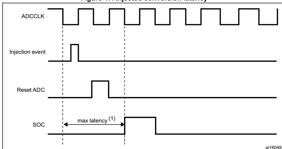
The timing diagram shows four signals over time:
- ADCCLK: A periodic square wave representing the ADC clock.
- Injection event: A signal that goes high for a short duration. A rising edge is aligned with a falling edge of the ADCCLK signal.
- Reset ADC: A signal that goes high in response to the injection event and then goes low after one ADC clock cycle.
- SOC (Start of Conversion): A signal that goes high when the injected conversion begins. A vertical dashed line indicates the start of the injection sequence.
- 1. The maximum latency value can be found in the electrical characteristics of the STM32F40x and STM32F41x datasheets.
13.3.10 Discontinuous mode
Regular group
This mode is enabled by setting the DISCEN bit in the ADC_CR1 register. It can be used to convert a short sequence of n conversions ( \( n \leq 8 \) ) that is part of the sequence of conversions selected in the ADC_SQRx registers. The value of n is specified by writing to the DISCNUM[2:0] bits in the ADC_CR1 register.
When an external trigger occurs, it starts the next n conversions selected in the ADC_SQRx registers until all the conversions in the sequence are done. The total sequence length is defined by the L[3:0] bits in the ADC_SQR1 register.
Example:
- • n = 3, channels to be converted = 0, 1, 2, 3, 6, 7, 9, 10
- • 1st trigger: sequence converted 0, 1, 2. An EOC event is generated at each conversion.
- • 2nd trigger: sequence converted 3, 6, 7. An EOC event is generated at each conversion
- • 3rd trigger: sequence converted 9, 10. An EOC event is generated at each conversion
- • 4th trigger: sequence converted 0, 1, 2. An EOC event is generated at each conversion
Note: When a regular group is converted in discontinuous mode, no rollover occurs.
When all subgroups are converted, the next trigger starts the conversion of the first subgroup. In the example above, the 4th trigger reconverts the channels 0, 1 and 2 in the 1st subgroup.
Injected group
This mode is enabled by setting the JDISCEN bit in the ADC_CR1 register. It can be used to convert the sequence selected in the ADC_JSQR register, channel by channel, after an external trigger event.
When an external trigger occurs, it starts the next channel conversions selected in the ADC_JSQR registers until all the conversions in the sequence are done. The total sequence length is defined by the JL[1:0] bits in the ADC_JSQR register.
Example:
n = 1, channels to be converted = 1, 2, 3
1st trigger: channel 1 converted
2nd trigger: channel 2 converted
3rd trigger: channel 3 converted and JEOC event generated
4th trigger: channel 1
Note: When all injected channels are converted, the next trigger starts the conversion of the first injected channel. In the example above, the 4th trigger reconverts the 1st injected channel 1.
It is not possible to use both the auto-injected and discontinuous modes simultaneously.
Discontinuous mode must not be set for regular and injected groups at the same time.
Discontinuous mode must be enabled only for the conversion of one group.
13.4 Data alignment
The ALIGN bit in the ADC_CR2 register selects the alignment of the data stored after conversion. Data can be right- or left-aligned as shown in Figure 48 and Figure 49 .
The converted data value from the injected group of channels is decreased by the user-defined offset written in the ADC_JOFRx registers so the result can be a negative value. The SEXT bit represents the extended sign value.
For channels in a regular group, no offset is subtracted so only twelve bits are significant.
Figure 48. Right alignment of 12-bit data
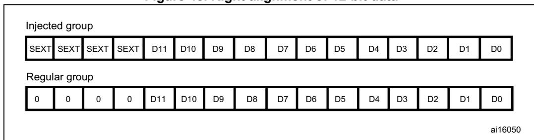
Diagram illustrating the right alignment of 12-bit data. The injected group consists of 16 bits: four SEXT bits followed by 12 data bits (D11 to D0). The regular group consists of 16 bits: four 0 bits followed by 12 data bits (D11 to D0). The identifier ai16050 is shown in the bottom right corner.
| Injected group | |||||||||||||||
| SEXT | SEXT | SEXT | SEXT | D11 | D10 | D9 | D8 | D7 | D6 | D5 | D4 | D3 | D2 | D1 | D0 |
| Regular group | |||||||||||||||
| 0 | 0 | 0 | 0 | D11 | D10 | D9 | D8 | D7 | D6 | D5 | D4 | D3 | D2 | D1 | D0 |
ai16050
Figure 49. Left alignment of 12-bit data
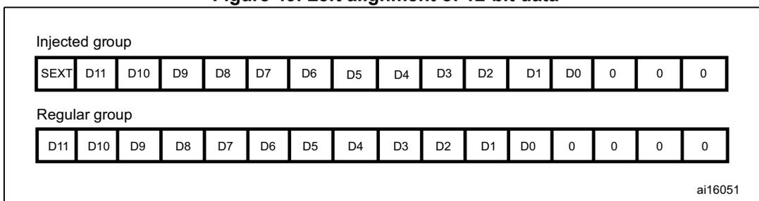
Diagram illustrating the left alignment of 12-bit data. The injected group consists of 16 bits: one SEXT bit, followed by 12 data bits (D11 to D0), and three 0 bits. The regular group consists of 16 bits: 12 data bits (D11 to D0) followed by four 0 bits. The identifier ai16051 is shown in the bottom right corner.
| Injected group | |||||||||||||||
| SEXT | D11 | D10 | D9 | D8 | D7 | D6 | D5 | D4 | D3 | D2 | D1 | D0 | 0 | 0 | 0 |
| Regular group | |||||||||||||||
| D11 | D10 | D9 | D8 | D7 | D6 | D5 | D4 | D3 | D2 | D1 | D0 | 0 | 0 | 0 | 0 |
ai16051
Special case: when left-aligned, the data are aligned on a half-word basis except when the resolution is set to 6-bit. In that case, the data are aligned on a byte basis as shown in Figure 50 .
Figure 50. Left alignment of 6-bit data
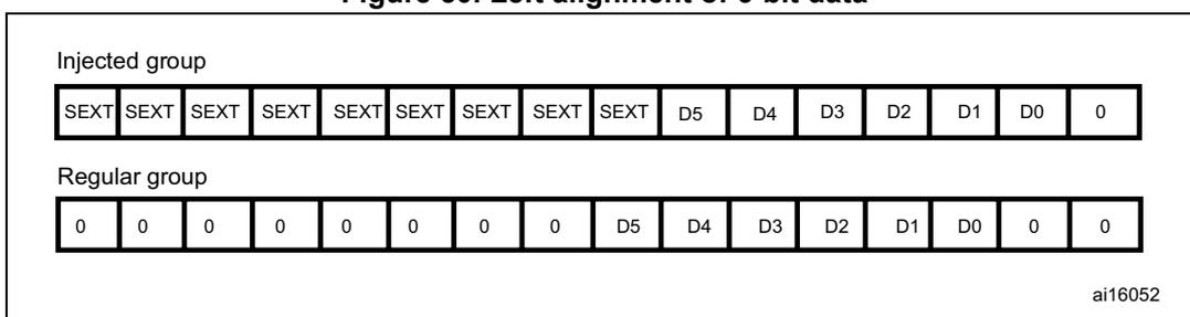
Diagram illustrating the left alignment of 6-bit data. The injected group consists of 16 bits: eight SEXT bits, followed by 6 data bits (D5 to D0), and two 0 bits. The regular group consists of 16 bits: five 0 bits, followed by 6 data bits (D5 to D0), and five 0 bits. The identifier ai16052 is shown in the bottom right corner.
| Injected group | |||||||||||||||
| SEXT | SEXT | SEXT | SEXT | SEXT | SEXT | SEXT | SEXT | D5 | D4 | D3 | D2 | D1 | D0 | 0 | 0 |
| Regular group | |||||||||||||||
| 0 | 0 | 0 | 0 | 0 | 0 | 0 | 0 | D5 | D4 | D3 | D2 | D1 | D0 | 0 | 0 |
ai16052
13.5 Channel-wise programmable sampling time
The ADC samples the input voltage for a number of ADCCLK cycles that can be modified using the SMP[2:0] bits in the ADC_SMPR1 and ADC_SMPR2 registers. Each channel can be sampled with a different sampling time.
The total conversion time is calculated as follows:
Example:
With ADCCLK = 30 MHz and sampling time = 3 cycles:
13.6 Conversion on external trigger and trigger polarity
Conversion can be triggered by an external event (e.g. timer capture, EXTI line). If the EXTEN[1:0] control bits (for a regular conversion) or JEXTEN[1:0] bits (for an injected conversion) are different from “0b00”, then external events are able to trigger a conversion with the selected polarity. Table 68 provides the correspondence between the EXTEN[1:0] and JEXTEN[1:0] values and the trigger polarity.
Table 68. Configuring the trigger polarity
| Source | EXTEN[1:0] / JEXTEN[1:0] |
|---|---|
| Trigger detection disabled | 00 |
| Detection on the rising edge | 01 |
| Detection on the falling edge | 10 |
| Detection on both the rising and falling edges | 11 |
Note: The polarity of the external trigger can be changed on the fly.
The EXTSEL[3:0] and JEXTSEL[3:0] control bits are used to select which out of 16 possible events can trigger conversion for the regular and injected groups.
Table 69 gives the possible external trigger for regular conversion.
Table 69. External trigger for regular channels| Source | Type | EXTSEL[3:0] |
|---|---|---|
| TIM1_CH1 event | Internal signal from on-chip timers | 0000 |
| TIM1_CH2 event | 0001 | |
| TIM1_CH3 event | 0010 | |
| TIM2_CH2 event | 0011 | |
| TIM2_CH3 event | 0100 | |
| TIM2_CH4 event | 0101 | |
| TIM2_TRGO event | 0110 | |
| TIM3_CH1 event | 0111 | |
| TIM3_TRGO event | 1000 | |
| TIM4_CH4 event | 1001 | |
| TIM5_CH1 event | 1010 | |
| TIM5_CH2 event | 1011 | |
| TIM5_CH3 event | 1100 | |
| TIM8_CH1 event | 1101 | |
| TIM8_TRGO event | 1110 | |
| EXTI line11 | External pin | 1111 |
Table 70 gives the possible external trigger for injected conversion.
Table 70. External trigger for injected channels
| Source | Connection type | JEXTSEL[3:0] |
|---|---|---|
| TIM1_CH4 event | Internal signal from on-chip timers | 0000 |
| TIM1_TRGO event | 0001 | |
| TIM2_CH1 event | 0010 | |
| TIM2_TRGO event | 0011 | |
| TIM3_CH2 event | 0100 | |
| TIM3_CH4 event | 0101 | |
| TIM4_CH1 event | 0110 | |
| TIM4_CH2 event | 0111 | |
| TIM4_CH3 event | 1000 | |
| TIM4_TRGO event | 1001 | |
| TIM5_CH4 event | 1010 | |
| TIM5_TRGO event | 1011 | |
| TIM8_CH2 event | 1100 | |
| TIM8_CH3 event | 1101 | |
| TIM8_CH4 event | 1110 | |
| EXTI line15 | External pin | 1111 |
Software source trigger events can be generated by setting SWSTART (for regular conversion) or JSWSTART (for injected conversion) in ADC_CR2.
A regular group conversion can be interrupted by an injected trigger.
Note: The trigger selection can be changed on the fly. However, when the selection changes, there is a time frame of 1 APB clock cycle during which the trigger detection is disabled. This is to avoid spurious detection during transitions.
13.7 Fast conversion mode
It is possible to perform faster conversion by reducing the ADC resolution. The RES bits are used to select the number of bits available in the data register. The minimum conversion time for each resolution is then as follows:
- • 12 bits: 3 + 12 = 15 ADCCLK cycles
- • 10 bits: 3 + 10 = 13 ADCCLK cycles
- • 8 bits: 3 + 8 = 11 ADCCLK cycles
- • 6 bits: 3 + 6 = 9 ADCCLK cycles
13.8 Data management
13.8.1 Using the DMA
Since converted regular channel values are stored into a unique data register, it is useful to use DMA for conversion of more than one regular channel. This avoids the loss of the data already stored in the ADC_DR register.
When the DMA mode is enabled (DMA bit set to 1 in the ADC_CR2 register), after each conversion of a regular channel, a DMA request is generated. This allows the transfer of the converted data from the ADC_DR register to the destination location selected by the software.
Despite this, if data are lost (overrun), the OVR bit in the ADC_SR register is set and an interrupt is generated (if the OVRIE enable bit is set). DMA transfers are then disabled and DMA requests are no longer accepted. In this case, if a DMA request is made, the regular conversion in progress is aborted and further regular triggers are ignored. It is then necessary to clear the OVR flag and the DMAEN bit in the used DMA stream, and to re-initialize both the DMA and the ADC to have the wanted converted channel data transferred to the right memory location. Only then can the conversion be resumed and the data transfer, enabled again. Injected channel conversions are not impacted by overrun errors.
When OVR = 1 in DMA mode, the DMA requests are blocked after the last valid data have been transferred, which means that all the data transferred to the RAM can be considered as valid.
At the end of the last DMA transfer (number of transfers configured in the DMA controller's DMA_SxNDTR register):
- • No new DMA request is issued to the DMA controller if the DDS bit is cleared to 0 in the ADC_CR2 register (this avoids generating an overrun error). However the DMA bit is not cleared by hardware. It must be written to 0, then to 1 to start a new transfer.
- • Requests can continue to be generated if the DDS bit is set to 1. This allows configuring the DMA in double-buffer circular mode.
To recover the ADC from OVR state when the DMA is used, follow the steps below:
- 1. Reinitialize the DMA (adjust destination address and NDTR counter)
- 2. Clear the ADC OVR bit in ADC_SR register
- 3. Trigger the ADC to start the conversion.
13.8.2 Managing a sequence of conversions without using the DMA
If the conversions are slow enough, the conversion sequence can be handled by the software. In this case the EOCS bit must be set in the ADC_CR2 register for the EOC status bit to be set at the end of each conversion, and not only at the end of the sequence. When EOCS = 1, overrun detection is automatically enabled. Thus, each time a conversion is complete, EOC is set and the ADC_DR register can be read. The overrun management is the same as when the DMA is used.
To recover the ADC from OVR state when the EOCS is set, follow the steps below:
- 1. Clear the ADC OVR bit in ADC_SR register
- 2. Trigger the ADC to start the conversion.
13.8.3 Conversions without DMA and without overrun detection
It may be useful to let the ADC convert one or more channels without reading the data each time (if there is an analog watchdog for instance). For that, the DMA must be disabled (DMA = 0) and the EOC bit must be set at the end of a sequence only (EOCS = 0). In this configuration, overrun detection is disabled.
13.9 Multi ADC mode
In devices with two ADCs or more, the Dual (with two ADCs) and Triple (with three ADCs) ADC modes can be used (see Figure 51 ).
In multi ADC mode, the start of conversion is triggered alternately or simultaneously by the ADC1 master to the ADC2 and ADC3 slaves, depending on the mode selected by the MULTI[4:0] bits in the ADC_CCR register.
Note: In multi ADC mode, when configuring conversion trigger by an external event, the application must set trigger by the master only and disable trigger by slaves to prevent spurious triggers that would start unwanted slave conversions.
The four possible modes below are implemented:
- • Injected simultaneous mode
- • Regular simultaneous mode
- • Interleaved mode
- • Alternate trigger mode
It is also possible to use the previous modes combined in the following ways:
- • Injected simultaneous mode + Regular simultaneous mode
- • Regular simultaneous mode + Alternate trigger mode
Note: In multi ADC mode, the converted data can be read on the multi-mode data register (ADC_CDR). The status bits can be read in the multi-mode status register (ADC_CSR).
Figure 51. Multi ADC block diagram (1)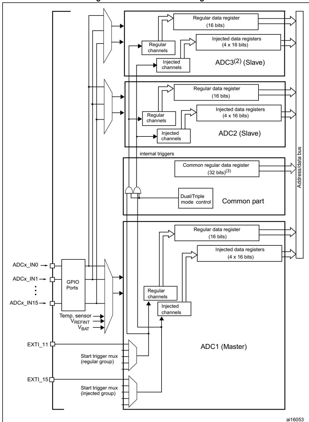
The diagram illustrates the internal architecture of the Multi ADC system. On the left, various input sources are shown: ADCx_IN0 through ADCx_IN15, a Temp. sensor, V REFINT , and V BAT connected to a 'GPIO Ports' block. External triggers EXT1_11 and EXT1_15 are connected to 'Start trigger mux (regular group)' and 'Start trigger mux (injected group)' blocks. These muxes feed into the ADC1 (Master) block. The ADC1 (Master) block contains 'Regular channels' and 'Injected channels' which connect to a 'Regular data register (16 bits)' and 'Injected data registers (4 x 16 bits)'. Above the master block is a 'Common part' containing a 'Common regular data register (32 bits) (3) ' and a 'Dual/Triple mode control' block. This common part receives 'internal triggers' and is connected to a vertical 'Address/data bus'. Above the common part are two slave blocks, ADC2 (Slave) and ADC3 (2) (Slave). Each slave block contains its own 'Regular channels', 'Injected channels', 'Regular data register (16 bits)', and 'Injected data registers (4 x 16 bits)', all connected to the common 'Address/data bus'.
ai16053
- 1. Although external triggers are present on ADC2 and ADC3 they are not shown in this diagram.
- 2. In the Dual ADC mode, the ADC3 slave part is not present.
- 3. In Triple ADC mode, the ADC common data register (ADC_CDR) contains the ADC1, ADC2 and ADC3's regular converted data. All 32 register bits are used according to a selected storage order.
In Dual ADC mode, the ADC common data register (ADC_CDR) contains both the ADC1 and ADC2's regular converted data. All 32 register bits are used.
- • DMA requests in Multi ADC mode:
In Multi ADC mode the DMA may be configured to transfer converted data in three different modes. In all cases, the DMA streams to use are those connected to the ADC:
- – DMA mode 1: On each DMA request (one data item is available), a half-word representing an ADC-converted data item is transferred.
In Triple ADC mode, ADC1 data are transferred on the first request, ADC2 data are transferred on the second request and ADC3 data are transferred on the third request; the sequence is repeated. So the DMA first transfers ADC1 data followed by ADC2 data followed by ADC3 data and so on.
DMA mode 1 is used in regular simultaneous triple mode only.
Example:
Regular simultaneous triple mode: 3 consecutive DMA requests are generated (one for each converted data item)
1st request: ADC_CDR[31:0] = ADC1_DR[15:0]
2nd request: ADC_CDR[31:0] = ADC2_DR[15:0]
3rd request: ADC_CDR[31:0] = ADC3_DR[15:0]
4th request: ADC_CDR[31:0] = ADC1_DR[15:0]
- – DMA mode 2: On each DMA request (two data items are available) two half-words representing two ADC-converted data items are transferred as a word.
In Dual ADC mode, both ADC2 and ADC1 data are transferred on the first request (ADC2 data take the upper half-word and ADC1 data take the lower half-word) and so on.
In Triple ADC mode, three DMA requests are generated. On the first request, both ADC2 and ADC1 data are transferred (ADC2 data take the upper half-word and ADC1 data take the lower half-word). On the second request, both ADC1 and ADC3 data are transferred (ADC1 data take the upper half-word and ADC3 data take the lower half-word). On the third request, both ADC3 and ADC2 data are transferred (ADC3 data take the upper half-word and ADC2 data take the lower half-word) and so on.
DMA mode 2 is used in interleaved mode and in regular simultaneous mode (for Dual ADC mode only).
Example:
- a) Interleaved dual mode: a DMA request is generated each time 2 data items are available:
1st request: ADC_CDR[31:0] = ADC2_DR[15:0] | ADC1_DR[15:0]
2nd request: ADC_CDR[31:0] = ADC2_DR[15:0] | ADC1_DR[15:0]
- b) Interleaved triple mode: a DMA request is generated each time 2 data items are available
1st request: ADC_CDR[31:0] = ADC2_DR[15:0] | ADC1_DR[15:0]
2nd request: ADC_CDR[31:0] = ADC1_DR[15:0] | ADC3_DR[15:0]
3rd request: ADC_CDR[31:0] = ADC3_DR[15:0] | ADC2_DR[15:0]
4th request: ADC_CDR[31:0] = ADC2_DR[15:0] | ADC1_DR[15:0]
- – DMA mode 3: This mode is similar to the DMA mode 2. The only differences are that the on each DMA request (two data items are available) two bytes
representing two ADC converted data items are transferred as a half-word. The data transfer order is similar to that of the DMA mode 2.
DMA mode 3 is used in interleaved mode in 6-bit and 8-bit resolutions (dual and triple mode).
Example:
- a) Interleaved dual mode: a DMA request is generated each time 2 data items are available
1st request: ADC_CDR[15:0] = ADC2_DR[7:0] | ADC1_DR[7:0]
2nd request: ADC_CDR[15:0] = ADC2_DR[7:0] | ADC1_DR[7:0] - b) Interleaved triple mode: a DMA request is generated each time 2 data items are available
1st request: ADC_CDR[15:0] = ADC2_DR[7:0] | ADC1_DR[7:0]
2nd request: ADC_CDR[15:0] = ADC1_DR[7:0] | ADC3_DR[7:0]
3rd request: ADC_CDR[15:0] = ADC3_DR[7:0] | ADC2_DR[7:0]
4th request: ADC_CDR[15:0] = ADC2_DR[7:0] | ADC1_DR[7:0]
Overrun detection: If an overrun is detected on one of the concerned ADCs (ADC1 and ADC2 in dual and triple modes, ADC3 in triple mode only), the DMA requests are no longer issued to ensure that all the data transferred to the RAM are valid. It may happen that the EOC bit corresponding to one ADC remains set because the data register of this ADC contains valid data.
13.9.1 Injected simultaneous mode
This mode converts an injected group of channels. The external trigger source comes from the injected group multiplexer of ADC1 (selected by the JEXTSEL[3:0] bits in the ADC1_CR2 register). A simultaneous trigger is provided to ADC2 and ADC3.
Note: Do not convert the same channel on the two/three ADCs (no overlapping sampling times for the two/three ADCs when converting the same channel).
In simultaneous mode, one must convert sequences with the same length or ensure that the interval between triggers is longer than the longer of the 2 sequences (Dual ADC mode) /3 sequences (Triple ADC mode). Otherwise, the ADC with the shortest sequence may restart while the ADC with the longest sequence is completing the previous conversions.
Regular conversions can be performed on one or all ADCs. In that case, they are independent of each other and are interrupted when an injected event occurs. They are resumed at the end of the injected conversion group.
Dual ADC mode
At the end of conversion event on ADC1 or ADC2:
- • The converted data are stored into the ADC_JDRx registers of each ADC interface.
- • A JEOC interrupt is generated (if enabled on one of the two ADC interfaces) when the ADC1/ADC2's injected channels have all been converted.
Figure 52. Injected simultaneous mode on 4 channels: dual ADC mode
Triple ADC mode
At the end of conversion event on ADC1, ADC2 or ADC3:
- • The converted data are stored into the ADC_JDRx registers of each ADC interface.
- • A JEOC interrupt is generated (if enabled on one of the three ADC interfaces) when the ADC1/ADC2/ADC3's injected channels have all been converted.
Figure 53. Injected simultaneous mode on 4 channels: triple ADC mode
13.9.2 Regular simultaneous mode
This mode is performed on a regular group of channels. The external trigger source comes from the regular group multiplexer of ADC1 (selected by the EXTSEL[3:0] bits in the ADC1_CR2 register). A simultaneous trigger is provided to ADC2 and ADC3.
Note: Do not convert the same channel on the two/three ADCs (no overlapping sampling times for the two/three ADCs when converting the same channel).
In regular simultaneous mode, one must convert sequences with the same length or ensure that the interval between triggers is longer than the long conversion time of the 2 sequences (Dual ADC mode) /3 sequences (Triple ADC mode). Otherwise, the ADC with the shortest sequence may restart while the ADC with the longest sequence is completing the previous conversions.
Injected conversions must be disabled.
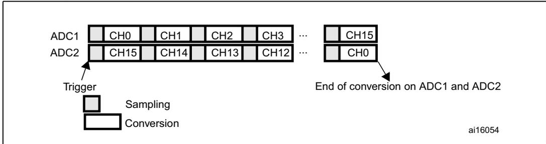
Dual ADC mode
At the end of conversion event on ADC1 or ADC2:
- • A 32-bit DMA transfer request is generated (if DMA[1:0] bits in the ADC_CCR register are equal to 0b10). This request transfers the ADC2 converted data stored in the upper half-word of the ADC_CDR 32-bit register to the SRAM and then the ADC1 converted data stored in the lower half-word of ADC_CDR to the SRAM.
- • An EOC interrupt is generated (if enabled on one of the two ADC interfaces) when the ADC1/ADC2's regular channels have all been converted.
Figure 54. Regular simultaneous mode on 16 channels: dual ADC mode
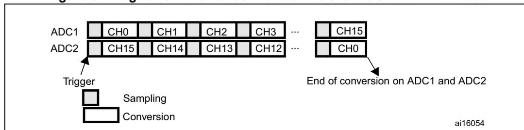
The diagram illustrates the timing for Dual ADC mode. It shows two horizontal timelines for ADC1 and ADC2. ADC1's sequence starts with a 'Trigger' and proceeds through sampling and conversion of channels CH0, CH1, CH2, CH3, ..., CH15. ADC2's sequence also starts with the same 'Trigger' and proceeds through sampling and conversion of channels CH15, CH14, CH13, CH12, ..., CH0. Both sequences have a 'Sampling' phase followed by a 'Conversion' phase. The 'End of conversion on ADC1 and ADC2' is indicated by an arrow pointing to the completion of both sequences. The identifier 'ai16054' is present in the bottom right corner.
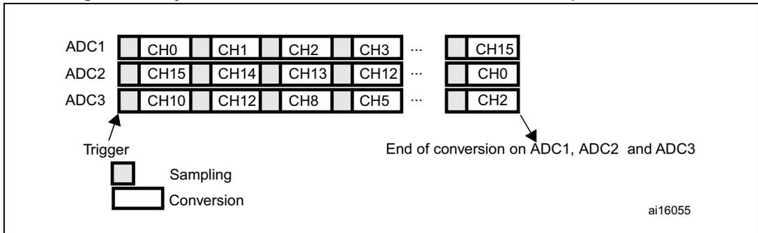
Triple ADC mode
At the end of conversion event on ADC1, ADC2 or ADC3:
- • Three 32-bit DMA transfer requests are generated (if DMA[1:0] bits in the ADC_CCR register are equal to 0b01). Three transfers then take place from the ADC_CDR 32-bit register to SRAM: first the ADC1 converted data, then the ADC2 converted data and finally the ADC3 converted data. The process is repeated for each new three conversions.
- • An EOC interrupt is generated (if enabled on one of the three ADC interfaces) when the ADC1/ADC2/ADC3's regular channels are have all been converted.
Figure 55. Regular simultaneous mode on 16 channels: triple ADC mode
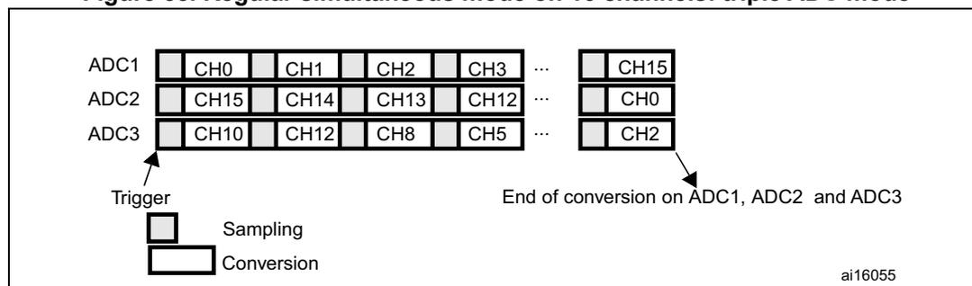
The diagram illustrates the timing for Triple ADC mode. It shows three horizontal timelines for ADC1, ADC2, and ADC3. ADC1's sequence starts with a 'Trigger' and proceeds through sampling and conversion of channels CH0, CH1, CH2, CH3, ..., CH15. ADC2's sequence also starts with the same 'Trigger' and proceeds through sampling and conversion of channels CH15, CH14, CH13, CH12, ..., CH0. ADC3's sequence starts with the same 'Trigger' and proceeds through sampling and conversion of channels CH10, CH12, CH8, CH5, ..., CH2. All three sequences have a 'Sampling' phase followed by a 'Conversion' phase. The 'End of conversion on ADC1, ADC2 and ADC3' is indicated by an arrow pointing to the completion of all three sequences. The identifier 'ai16055' is present in the bottom right corner.
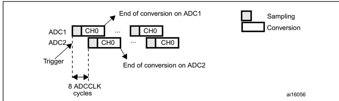
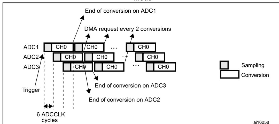
13.9.3 Interleaved mode
This mode can be started only on a regular group (usually one channel). The external trigger source comes from the regular channel multiplexer of ADC1.
Dual ADC mode
After an external trigger occurs:
- • ADC1 starts immediately
- • ADC2 starts after a delay of several-ADC clock cycles
The minimum delay which separates 2 conversions in interleaved mode is configured in the DELAY bits in the ADC_CCR register. However, an ADC cannot start a conversion if the complementary ADC is still sampling its input (only one ADC can sample the input signal at a given time). In this case, the delay becomes the sampling time + 2 ADC clock cycles. For instance, if DELAY = 5 clock cycles and the sampling takes 15 clock cycles on both ADCs, then 17 clock cycles separate conversions on ADC1 and ADC2).
If the CONT bit is set on both ADC1 and ADC2, the selected regular channels of both ADCs are continuously converted.
Note: If the conversion sequence is interrupted (for instance when DMA end of transfer occurs), the multi-ADC sequencer must be reset by configuring it in independent mode first (bits DUAL[4:0] = 00000) before reprogramming the interleaved mode.
After an EOC interrupt is generated by ADC2 (if enabled through the EOCIE bit) a 32-bit DMA transfer request is generated (if the DMA[1:0] bits in ADC_CCR are equal to 0b10). This request first transfers the ADC2 converted data stored in the upper half-word of the ADC_CDR 32-bit register into SRAM, then the ADC1 converted data stored in the register's lower half-word into SRAM.
Figure 56. Interleaved mode on 1 channel in continuous conversion mode: dual ADC mode
Triple ADC mode
After an external trigger occurs:
- • ADC1 starts immediately and
- • ADC2 starts after a delay of several ADC clock cycles
- • ADC3 starts after a delay of several ADC clock cycles referred to the ADC2 conversion
The minimum delay which separates 2 conversions in interleaved mode is configured in the DELAY bits in the ADC_CCR register. However, an ADC cannot start a conversion if the complementary ADC is still sampling its input (only one ADC can sample the input signal at
a given time). In this case, the delay becomes the sampling time + 2 ADC clock cycles. For instance, if DELAY = 5 clock cycles and the sampling takes 15 clock cycles on the three ADCs, then 17 clock cycles separate the conversions on ADC1, ADC2 and ADC3).
If the CONT bit is set on ADC1, ADC2 and ADC3, the selected regular channels of all ADCs are continuously converted.
Note: If the conversion sequence is interrupted (for instance when DMA end of transfer occurs), the multi-ADC sequencer must be reset by configuring it in independent mode first (bits DUAL[4:0] = 00000) before reprogramming the interleaved mode.
In this mode a DMA request is generated each time 2 data items are available, (if the DMA[1:0] bits in the ADC_CCR register are equal to 0b10). The request first transfers the first converted data stored in the lower half-word of the ADC_CDR 32-bit register to SRAM, then it transfers the second converted data stored in ADC_CDR's upper half-word to SRAM. The sequence is the following:
- • 1st request: \( ADC\_CDR[31:0] = ADC2\_DR[15:0] \mid ADC1\_DR[15:0] \)
- • 2nd request: \( ADC\_CDR[31:0] = ADC1\_DR[15:0] \mid ADC3\_DR[15:0] \)
- • 3rd request: \( ADC\_CDR[31:0] = ADC3\_DR[15:0] \mid ADC2\_DR[15:0] \)
- • 4th request: \( ADC\_CDR[31:0] = ADC2\_DR[15:0] \mid ADC1\_DR[15:0] \) , ...
Figure 57. Interleaved mode on 1 channel in continuous conversion mode: triple ADC mode
13.9.4 Alternate trigger mode
This mode can be started only on an injected group. The source of external trigger comes from the injected group multiplexer of ADC1.
Note: Regular conversions can be enabled on one or all ADCs. In this case the regular conversions are independent of each other. A regular conversion is interrupted when the
ADC has to perform an injected conversion. It is resumed when the injected conversion is finished.
If the conversion sequence is interrupted (for instance when DMA end of transfer occurs), the multi-ADC sequencer must be reset by configuring it in independent mode first (bits DUAL[4:0] = 00000) before reprogramming the interleaved mode.
The time interval between 2 trigger events must be greater than or equal to 1 ADC clock period. The minimum time interval between 2 trigger events that start conversions on the same ADC is the same as in the single ADC mode.
Dual ADC mode
- • When the 1st trigger occurs, all injected ADC1 channels in the group are converted
- • When the 2nd trigger occurs, all injected ADC2 channels in the group are converted
- • and so on
A JEOC interrupt, if enabled, is generated after all injected ADC1 channels in the group have been converted.
A JEOC interrupt, if enabled, is generated after all injected ADC2 channels in the group have been converted.
If another external trigger occurs after all injected channels in the group have been converted then the alternate trigger process restarts by converting the injected ADC1 channels in the group.
Figure 58. Alternate trigger: injected group of each ADC
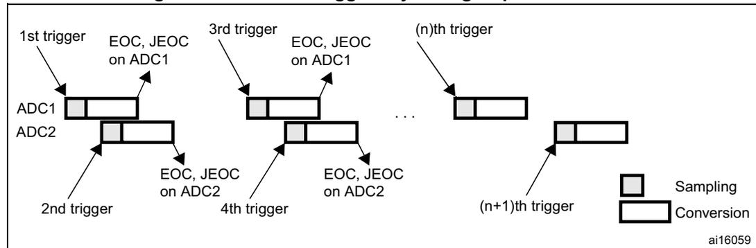
The diagram illustrates the timing of injected conversions in Dual ADC mode. It shows a sequence of triggers (1st, 2nd, 3rd, 4th, ..., (n)th, (n+1)th) and the corresponding ADC1 and ADC2 conversion phases. Each phase consists of a 'Sampling' block followed by a 'Conversion' block. The 1st trigger starts the ADC1 conversion. The 2nd trigger starts the ADC2 conversion. The 3rd trigger restarts the ADC1 conversion. The 4th trigger restarts the ADC2 conversion. This pattern continues. End-of-conversion (EOC, JEOC) signals are indicated for each conversion phase. A legend at the bottom right identifies the blocks as 'Sampling' and 'Conversion'. The diagram is labeled ai16059.
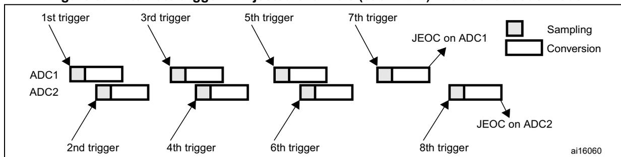
If the injected discontinuous mode is enabled for both ADC1 and ADC2:
- • When the 1st trigger occurs, the first injected ADC1 channel is converted.
- • When the 2nd trigger occurs, the first injected ADC2 channel are converted
- • and so on
A JEOC interrupt, if enabled, is generated after all injected ADC1 channels in the group have been converted.
A JEOC interrupt, if enabled, is generated after all injected ADC2 channels in the group have been converted.
If another external trigger occurs after all injected channels in the group have been converted then the alternate trigger process restarts.
Figure 59. Alternate trigger: 4 injected channels (each ADC) in discontinuous mode
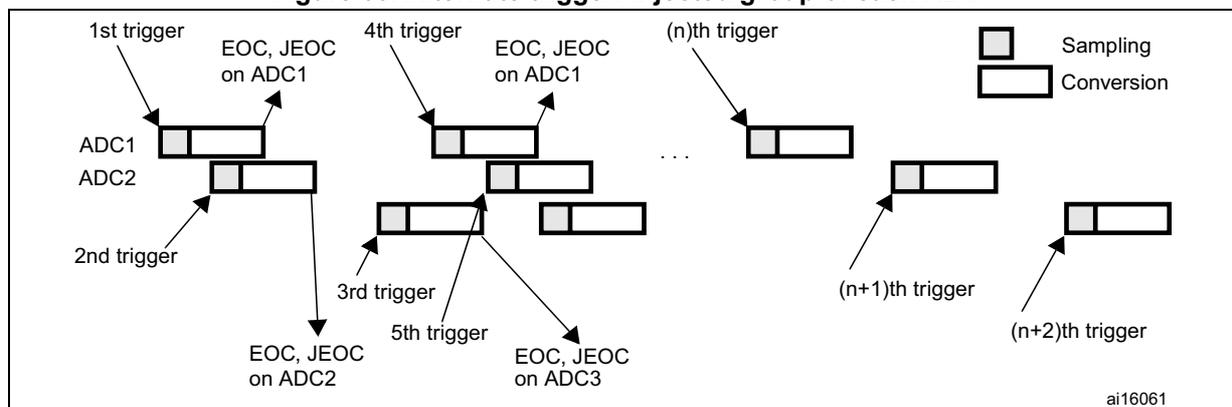
Triple ADC mode
- • When the 1st trigger occurs, all injected ADC1 channels in the group are converted.
- • When the 2nd trigger occurs, all injected ADC2 channels in the group are converted.
- • When the 3rd trigger occurs, all injected ADC3 channels in the group are converted.
- • and so on
A JEOC interrupt, if enabled, is generated after all injected ADC1 channels in the group have been converted.
A JEOC interrupt, if enabled, is generated after all injected ADC2 channels in the group have been converted.
A JEOC interrupt, if enabled, is generated after all injected ADC3 channels in the group have been converted.
If another external trigger occurs after all injected channels in the group have been converted then the alternate trigger process restarts by converting the injected ADC1 channels in the group.
Figure 60. Alternate trigger: injected group of each ADC
13.9.5 Combined regular/injected simultaneous mode
It is possible to interrupt the simultaneous conversion of a regular group to start the simultaneous conversion of an injected group.
Note: In combined regular/injected simultaneous mode, one must convert sequences with the same length or ensure that the interval between triggers is longer than the long conversion time of the 2 sequences (Dual ADC mode) /3 sequences (Triple ADC mode). Otherwise, the
ADC with the shortest sequence may restart while the ADC with the longest sequence is completing the previous conversions.
13.9.6 Combined regular simultaneous + alternate trigger mode
It is possible to interrupt the simultaneous conversion of a regular group to start the alternate trigger conversion of an injected group. Figure 61 shows the behavior of an alternate trigger interrupting a simultaneous regular conversion.
The injected alternate conversion is immediately started after the injected event. If regular conversion is already running, in order to ensure synchronization after the injected conversion, the regular conversion of all (master/slave) ADCs is stopped and resumed synchronously at the end of the injected conversion.
Note: In combined regular simultaneous + alternate trigger mode, one must convert sequences with the same length or ensure that the interval between triggers is longer than the long conversion time of the 2 sequences (Dual ADC mode) /3 sequences (Triple ADC mode). Otherwise, the ADC with the shortest sequence may restart while the ADC with the longest sequence is completing the previous conversions.
If the conversion sequence is interrupted (for instance when DMA end of transfer occurs), the multi-ADC sequencer must be reset by configuring it in independent mode first (bits DUAL[4:0] = 00000) before reprogramming the interleaved mode.
Figure 61. Alternate + regular simultaneous
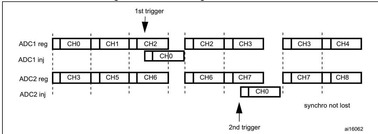
The diagram shows four horizontal timelines representing ADC conversion sequences over time.
1.
ADC1 reg
: Shows a sequence of channels CH0, CH1, CH2. When the sequence ends, it restarts with CH2, CH3, then CH3, CH4.
2.
ADC1 inj
: Shows an injected sequence starting with CH0.
3.
ADC2 reg
: Shows a sequence of channels CH3, CH5, CH6. When the sequence ends, it restarts with CH6, CH7, then CH7, CH8.
4.
ADC2 inj
: Shows an injected sequence starting with CH0.
A downward arrow labeled
1st trigger
occurs at the end of the first regular sequence (after CH2). This triggers the start of the injected sequence (CH0) for both ADC1 and ADC2.
A second downward arrow labeled
2nd trigger
occurs at the end of the injected sequence (after CH0). At this point, the regular sequences resume from where they left off (CH2 for ADC1, CH6 for ADC2).
The text
synchro not lost
is present in the bottom right, indicating that the regular sequences resume correctly after the injected conversion.
The identifier
ai16062
is in the bottom right corner of the diagram area.
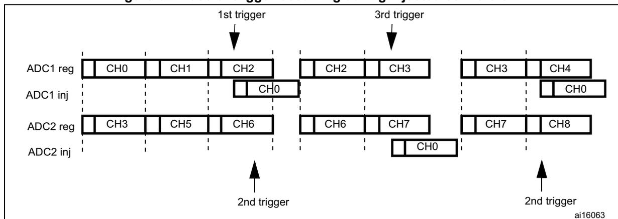
If a trigger occurs during an injected conversion that has interrupted a regular conversion, it is ignored. Figure 62 shows the behavior in this case (2nd trigger is ignored).
Figure 62. Case of trigger occurring during injected conversion
13.10 Temperature sensor
The temperature sensor can be used to measure the junction temperature ( \( T_j \) ) of the device.
- • On STM32F40x and STM32F41x devices, the temperature sensor is internally connected to ADC1_IN16 channel which is used to convert the sensor output voltage to a digital value.
- • On STM32F42x and STM32F43x devices, the temperature sensor is internally connected to the same input channel, ADC1_IN18, as VBAT: ADC1_IN18 is used to convert the sensor output voltage or VBAT into a digital value. Only one conversion, temperature sensor or VBAT, must be selected at a time. When the temperature sensor and the VBAT conversion are set simultaneously, only the VBAT conversion is performed.
Figure 63 shows the block diagram of the temperature sensor.
When not in use, the sensor can be put in power down mode.
Note: The TSVREFE bit must be set to enable the conversion of both internal channels: the ADC1_IN16 or ADC1_IN18 (temperature sensor) and the ADC1_IN17 (VREFINT).
Main features
- • Supported temperature range: \( -40 \) to \( 125 \) °C
- • Precision: \( \pm 1.5 \) °C
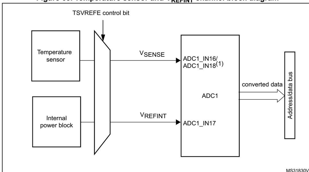
- 1. V SENSE is input to ADC1_IN16 for the STM23F40x and STM32F41x devices and to ADC1_IN18 for the STM32F42x and STM32F43x devices.
Reading the temperature
To use the sensor:
- 3. Select ADC1_IN16 or ADC1_IN18 input channel.
- 4. Select a sampling time greater than the minimum sampling time specified in the datasheet.
- 5. Set the TSVREFE bit in the ADC_CCR register to wake up the temperature sensor from power down mode
- 6. Start the ADC conversion by setting the SWSTART bit (or by external trigger)
- 7. Read the resulting V SENSE data in the ADC data register
- 8. Calculate the temperature using the following formula:
Where:
- – V 25 = V SENSE value for 25° C
- – Avg_Slope = average slope of the temperature vs. V SENSE curve (given in mV/°C or µV/°C)
Refer to the datasheet's electrical characteristics section for the actual values of V 25 and Avg_Slope.
Note: The sensor has a startup time after waking from power down mode before it can output V SENSE at the correct level. The ADC also has a startup time after power-on, so to minimize the delay, the ADON and TSVREFE bits should be set at the same time.
The temperature sensor output voltage changes linearly with temperature. The offset of this linear function depends on each chip due to process variation (up to 45 °C from one chip to another).
The internal temperature sensor is more suited for applications that detect temperature variations instead of absolute temperatures. If accurate temperature reading is required, an external temperature sensor should be used.
13.11 Battery charge monitoring
The VBATE bit in the ADC_CCR register is used to switch to the battery voltage. As the \( V_{BAT} \) voltage could be higher than \( V_{DDA} \) , to ensure the correct operation of the ADC, the \( V_{BAT} \) pin is internally connected to a bridge divider.
When the VBATE is set, the bridge is automatically enabled to connect:
- • \( V_{BAT}/2 \) to the ADC1_IN18 input channel, on STM32F40xx and STM32F41xx devices
- • \( V_{BAT}/4 \) to the ADC1_IN18 input channel, on STM32F42xx and STM32F43xx devices
Note: On STM32F42xx and STM32F43xx devices, VBAT and temperature sensor are connected to the same ADC internal channel (ADC1_IN18). Only one conversion, either temperature sensor or VBAT, must be selected at a time. When both conversion are enabled simultaneously, only the VBAT conversion is performed.
13.12 ADC interrupts
An interrupt can be produced on the end of conversion for regular and injected groups, when the analog watchdog status bit is set and when the overrun status bit is set. Separate interrupt enable bits are available for flexibility.
Two other flags are present in the ADC_SR register, but there is no interrupt associated with them:
- • JSTRT (Start of conversion for channels of an injected group)
- • STRT (Start of conversion for channels of a regular group)
Table 71. ADC interrupts
| Interrupt event | Event flag | Enable control bit |
|---|---|---|
| End of conversion of a regular group | EOC | EOCIE |
| End of conversion of an injected group | JEOC | JEOCIE |
| Analog watchdog status bit is set | AWD | AWDIE |
| Overrun | OVR | OVRIE |
13.13 ADC registers
Refer to Section 1.1: List of abbreviations for registers for registers for a list of abbreviations used in register descriptions.
The peripheral registers must be written at word level (32 bits). Read accesses can be done by bytes (8 bits), half-words (16 bits) or words (32 bits).
13.13.1 ADC status register (ADC_SR)
Address offset: 0x00
Reset value: 0x0000 0000
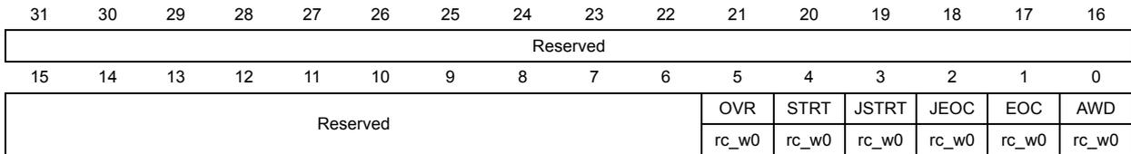
| 31 | 30 | 29 | 28 | 27 | 26 | 25 | 24 | 23 | 22 | 21 | 20 | 19 | 18 | 17 | 16 |
| Reserved | |||||||||||||||
| 15 | 14 | 13 | 12 | 11 | 10 | 9 | 8 | 7 | 6 | 5 | 4 | 3 | 2 | 1 | 0 |
| Reserved | OVR rc_w0 | STRT rc_w0 | JSTRT rc_w0 | JEOC rc_w0 | EOC rc_w0 | AWD rc_w0 | |||||||||
Bits 31:6 Reserved, must be kept at reset value.
Bit 5 OVR : Overrun
This bit is set by hardware when data are lost (either in single mode or in dual/triple mode). It is cleared by software. Overrun detection is enabled only when DMA = 1 or EOCS = 1.
0: No overrun occurred
1: Overrun has occurred
Bit 4 STRT : Regular channel start flag
This bit is set by hardware when regular channel conversion starts. It is cleared by software.
0: No regular channel conversion started
1: Regular channel conversion has started
Bit 3 JSTRT : Injected channel start flag
This bit is set by hardware when injected group conversion starts. It is cleared by software.
0: No injected group conversion started
1: Injected group conversion has started
Bit 2 JEOC : Injected channel end of conversion
This bit is set by hardware at the end of the conversion of all injected channels in the group. It is cleared by software.
0: Conversion is not complete
1: Conversion complete
Bit 1 EOC : Regular channel end of conversion
This bit is set by hardware at the end of the conversion of a regular group of channels. It is cleared by software or by reading the ADC_DR register.
0: Conversion not complete (EOCS=0), or sequence of conversions not complete (EOCS=1)
1: Conversion complete (EOCS=0), or sequence of conversions complete (EOCS=1)
Bit 0 AWD : Analog watchdog flag
This bit is set by hardware when the converted voltage crosses the values programmed in the ADC_LTR and ADC_HTR registers. It is cleared by software.
0: No analog watchdog event occurred
1: Analog watchdog event occurred
13.13.2 ADC control register 1 (ADC_CR1)
Address offset: 0x04
Reset value: 0x0000 0000
| 31 | 30 | 29 | 28 | 27 | 26 | 25 | 24 | 23 | 22 | 21 | 20 | 19 | 18 | 17 | 16 |
|---|---|---|---|---|---|---|---|---|---|---|---|---|---|---|---|
| Reserved | OVRIE | RES | AWDEN | JAWDEN | Reserved | ||||||||||
| rw | rw | rw | rw | rw | |||||||||||
| 15 | 14 | 13 | 12 | 11 | 10 | 9 | 8 | 7 | 6 | 5 | 4 | 3 | 2 | 1 | 0 |
| DISCNUM[2:0] | JDISCEN | DISCEN | JAUTO | AWDSGL | SCAN | JEOCIE | AWDIE | EOCIE | AWDCH[4:0] | ||||||
| rw | rw | rw | rw | rw | rw | rw | rw | ||||||||
Bits 31:27 Reserved, must be kept at reset value.
Bit 26 OVRIE : Overrun interrupt enable
This bit is set and cleared by software to enable/disable the Overrun interrupt.
0: Overrun interrupt disabled
1: Overrun interrupt enabled. An interrupt is generated when the OVR bit is set.
Bits 25:24 RES[1:0] : Resolution
These bits are written by software to select the resolution of the conversion.
00: 12-bit (15 ADCCLK cycles)
01: 10-bit (13 ADCCLK cycles)
10: 8-bit (11 ADCCLK cycles)
11: 6-bit (9 ADCCLK cycles)
Bit 23 AWDEN : Analog watchdog enable on regular channels
This bit is set and cleared by software.
0: Analog watchdog disabled on regular channels
1: Analog watchdog enabled on regular channels
Bit 22 JAWDEN : Analog watchdog enable on injected channels
This bit is set and cleared by software.
0: Analog watchdog disabled on injected channels
1: Analog watchdog enabled on injected channels
Bits 21:16 Reserved, must be kept at reset value.
Bits 15:13 DISCNUM[2:0] : Discontinuous mode channel count
These bits are written by software to define the number of regular channels to be converted in discontinuous mode, after receiving an external trigger.
000: 1 channel
001: 2 channels
...
111: 8 channels
Bit 12 JDISCEN : Discontinuous mode on injected channels
This bit is set and cleared by software to enable/disable discontinuous mode on the injected channels of a group.
0: Discontinuous mode on injected channels disabled
1: Discontinuous mode on injected channels enabled
Bit 11 DISCEN: Discontinuous mode on regular channelsThis bit is set and cleared by software to enable/disable Discontinuous mode on regular channels.
0: Discontinuous mode on regular channels disabled
1: Discontinuous mode on regular channels enabled
Bit 10 JAUTO: Automatic injected group conversionThis bit is set and cleared by software to enable/disable automatic injected group conversion after regular group conversion.
0: Automatic injected group conversion disabled
1: Automatic injected group conversion enabled
Bit 9 AWDSGL: Enable the watchdog on a single channel in scan modeThis bit is set and cleared by software to enable/disable the analog watchdog on the channel identified by the AWDCH[4:0] bits.
0: Analog watchdog enabled on all channels
1: Analog watchdog enabled on a single channel
Bit 8 SCAN: Scan modeThis bit is set and cleared by software to enable/disable the Scan mode. In Scan mode, the inputs selected through the ADC_SQRx or ADC_JSQRx registers are converted.
0: Scan mode disabled
1: Scan mode enabled
Note: An EOC interrupt is generated if the EOCIE bit is set:
- – At the end of each regular group sequence if the EOCS bit is cleared to 0
- – At the end of each regular channel conversion if the EOCS bit is set to 1
Note: A JEOC interrupt is generated only on the end of conversion of the last channel if the JEOCIE bit is set.
Bit 7 JEOCIE: Interrupt enable for injected channelsThis bit is set and cleared by software to enable/disable the end of conversion interrupt for injected channels.
0: JEOC interrupt disabled
1: JEOC interrupt enabled. An interrupt is generated when the JEOC bit is set.
Bit 6 AWDIE: Analog watchdog interrupt enableThis bit is set and cleared by software to enable/disable the analog watchdog interrupt.
0: Analog watchdog interrupt disabled
1: Analog watchdog interrupt enabled
Bit 5 EOCIE: Interrupt enable for EOCThis bit is set and cleared by software to enable/disable the end of conversion interrupt.
0: EOC interrupt disabled
1: EOC interrupt enabled. An interrupt is generated when the EOC bit is set.
Bits 4:0 AWDCH[4:0]: Analog watchdog channel select bitsThese bits are set and cleared by software. They select the input channel to be guarded by the analog watchdog.
Note: 00000: ADC analog input Channel0
00001: ADC analog input Channel1
...
01111: ADC analog input Channel15
10000: ADC analog input Channel16
10001: ADC analog input Channel17
10010: ADC analog input Channel18
Other values reserved
13.13.3 ADC control register 2 (ADC_CR2)
Address offset: 0x08
Reset value: 0x0000 0000
| 31 | 30 | 29 | 28 | 27 | 26 | 25 | 24 | 23 | 22 | 21 | 20 | 19 | 18 | 17 | 16 |
|---|---|---|---|---|---|---|---|---|---|---|---|---|---|---|---|
| reserved | SWSTART | EXTEN | EXTSEL[3:0] | reserved | JSWSTART | JEXTEN | JEXTSEL[3:0] | ||||||||
| rw | rw | rw | rw | rw | rw | rw | rw | rw | rw | rw | rw | rw | rw | ||
| 15 | 14 | 13 | 12 | 11 | 10 | 9 | 8 | 7 | 6 | 5 | 4 | 3 | 2 | 1 | 0 |
| reserved | ALIGN | EOCS | DDS | DMA | Reserved | CONT | ADON | ||||||||
| rw | rw | rw | rw | rw | rw | ||||||||||
Bit 31 Reserved, must be kept at reset value.
Bit 30 SWSTART : Start conversion of regular channels
This bit is set by software to start conversion and cleared by hardware as soon as the conversion starts.
0: Reset state
1: Starts conversion of regular channels
Note: This bit can be set only when ADON = 1 otherwise no conversion is launched.
Bits 29:28 EXTEN : External trigger enable for regular channels
These bits are set and cleared by software to select the external trigger polarity and enable the trigger of a regular group.
00: Trigger detection disabled
01: Trigger detection on the rising edge
10: Trigger detection on the falling edge
11: Trigger detection on both the rising and falling edges
Bits 27:24 EXTSEL[3:0] : External event select for regular group
These bits select the external event used to trigger the start of conversion of a regular group:
0000: Timer 1 CC1 event
0001: Timer 1 CC2 event
0010: Timer 1 CC3 event
0011: Timer 2 CC2 event
0100: Timer 2 CC3 event
0101: Timer 2 CC4 event
0110: Timer 2 TRGO event
0111: Timer 3 CC1 event
1000: Timer 3 TRGO event
1001: Timer 4 CC4 event
1010: Timer 5 CC1 event
1011: Timer 5 CC2 event
1100: Timer 5 CC3 event
1101: Timer 8 CC1 event
1110: Timer 8 TRGO event
1111: EXTI line11
Bit 23 Reserved, must be kept at reset value.
Bit 22 JSWSTART : Start conversion of injected channels
This bit is set by software and cleared by hardware as soon as the conversion starts.
0: Reset state
1: Starts conversion of injected channels
Note: This bit can be set only when ADON = 1 otherwise no conversion is launched.
Bits 21:20 JEXTEN : External trigger enable for injected channels
These bits are set and cleared by software to select the external trigger polarity and enable the trigger of an injected group.
00: Trigger detection disabled
01: Trigger detection on the rising edge
10: Trigger detection on the falling edge
11: Trigger detection on both the rising and falling edges
Bits 19:16 JEXTSEL[3:0] : External event select for injected group
These bits select the external event used to trigger the start of conversion of an injected group.
0000: Timer 1 CC4 event
0001: Timer 1 TRGO event
0010: Timer 2 CC1 event
0011: Timer 2 TRGO event
0100: Timer 3 CC2 event
0101: Timer 3 CC4 event
0110: Timer 4 CC1 event
0111: Timer 4 CC2 event
1000: Timer 4 CC3 event
1001: Timer 4 TRGO event
1010: Timer 5 CC4 event
1011: Timer 5 TRGO event
1100: Timer 8 CC2 event
1101: Timer 8 CC3 event
1110: Timer 8 CC4 event
1111: EXTI line15
Bits 15:12 Reserved, must be kept at reset value.
Bit 11 ALIGN : Data alignment
This bit is set and cleared by software. Refer to Figure 48 and Figure 49 .
0: Right alignment
1: Left alignment
Bit 10 EOCS : End of conversion selection
This bit is set and cleared by software.
0: The EOC bit is set at the end of each sequence of regular conversions. Overrun detection is enabled only if DMA=1.
1: The EOC bit is set at the end of each regular conversion. Overrun detection is enabled.
Bit 9 DDS : DMA disable selection (for single ADC mode)
This bit is set and cleared by software.
0: No new DMA request is issued after the last transfer (as configured in the DMA controller)
1: DMA requests are issued as long as data are converted and DMA=1
Bit 8 DMA : Direct memory access mode (for single ADC mode)
This bit is set and cleared by software. Refer to the DMA controller chapter for more details.
0: DMA mode disabled
1: DMA mode enabled
Bits 7:2 Reserved, must be kept at reset value.
Bit 1 CONT : Continuous conversion
This bit is set and cleared by software. If it is set, conversion takes place continuously until it is cleared.
0: Single conversion mode
1: Continuous conversion mode
Bit 0 ADON : A/D Converter ON / OFF
This bit is set and cleared by software.
Note: 0: Disable ADC conversion and go to power down mode
1: Enable ADC
13.13.4 ADC sample time register 1 (ADC_SMPR1)
Address offset: 0x0C
Reset value: 0x0000 0000
| 31 | 30 | 29 | 28 | 27 | 26 | 25 | 24 | 23 | 22 | 21 | 20 | 19 | 18 | 17 | 16 |
|---|---|---|---|---|---|---|---|---|---|---|---|---|---|---|---|
| Reserved | rw | SMP18[2:0] | SMP17[2:0] | SMP16[2:0] | SMP15[2:1] | ||||||||||
| rw | rw | rw | rw | rw | rw | rw | rw | rw | rw | ||||||
| 15 | 14 | 13 | 12 | 11 | 10 | 9 | 8 | 7 | 6 | 5 | 4 | 3 | 2 | 1 | 0 |
| SMP15_0 | SMP14[2:0] | SMP13[2:0] | SMP12[2:0] | SMP11[2:0] | SMP10[2:0] | ||||||||||
| rw | rw | rw | rw | rw | rw | rw | rw | rw | rw | rw | rw | rw | rw | rw | rw |
Bits 31: 27 Reserved, must be kept at reset value.
Bits 26:0 SMPx[2:0] : Channel x sampling time selection
These bits are written by software to select the sampling time individually for each channel. During sampling cycles, the channel selection bits must remain unchanged.
Note: 000: 3 cycles
001: 15 cycles
010: 28 cycles
011: 56 cycles
100: 84 cycles
101: 112 cycles
110: 144 cycles
111: 480 cycles
13.13.5 ADC sample time register 2 (ADC_SMPR2)
Address offset: 0x10
Reset value: 0x0000 0000
| 31 | 30 | 29 | 28 | 27 | 26 | 25 | 24 | 23 | 22 | 21 | 20 | 19 | 18 | 17 | 16 |
|---|---|---|---|---|---|---|---|---|---|---|---|---|---|---|---|
| Reserved | rw | SMP9[2:0] | SMP8[2:0] | SMP7[2:0] | SMP6[2:0] | SMP5[2:1] | |||||||||
| rw | rw | rw | rw | rw | rw | rw | rw | rw | rw | rw | rw | rw | |||
| 15 | 14 | 13 | 12 | 11 | 10 | 9 | 8 | 7 | 6 | 5 | 4 | 3 | 2 | 1 | 0 |
| SMP5_0 | SMP4[2:0] | SMP3[2:0] | SMP2[2:0] | SMP1[2:0] | SMP0[2:0] | ||||||||||
| rw | rw | rw | rw | rw | rw | rw | rw | rw | rw | rw | rw | rw | rw | rw | rw |
Bits 31:30 Reserved, must be kept at reset value.
Bits 29:0 SMPx[2:0] : Channel x sampling time selection
These bits are written by software to select the sampling time individually for each channel. During sample cycles, the channel selection bits must remain unchanged.
- Note:
- 000: 3 cycles
- 001: 15 cycles
- 010: 28 cycles
- 011: 56 cycles
- 100: 84 cycles
- 101: 112 cycles
- 110: 144 cycles
- 111: 480 cycles
13.13.6 ADC injected channel data offset register x (ADC_JOFRx) (x=1..4)
Address offset: 0x14-0x20
Reset value: 0x0000 0000
| 31 | 30 | 29 | 28 | 27 | 26 | 25 | 24 | 23 | 22 | 21 | 20 | 19 | 18 | 17 | 16 |
|---|---|---|---|---|---|---|---|---|---|---|---|---|---|---|---|
| Reserved | |||||||||||||||
| 15 | 14 | 13 | 12 | 11 | 10 | 9 | 8 | 7 | 6 | 5 | 4 | 3 | 2 | 1 | 0 |
| Reserved | JOFFSETx[11:0] | ||||||||||||||
| rw | rw | rw | rw | rw | rw | rw | rw | rw | rw | rw | rw | ||||
Bits 31:12 Reserved, must be kept at reset value.
Bits 11:0 JOFFSETx[11:0] : Data offset for injected channel x
These bits are written by software to define the offset to be subtracted from the raw converted data when converting injected channels. The conversion result can be read from in the ADC_JDRx registers.
13.13.7 ADC watchdog higher threshold register (ADC_HTR)
Address offset: 0x24
Reset value: 0x0000 0FFF
| 31 | 30 | 29 | 28 | 27 | 26 | 25 | 24 | 23 | 22 | 21 | 20 | 19 | 18 | 17 | 16 |
|---|---|---|---|---|---|---|---|---|---|---|---|---|---|---|---|
| Reserved | |||||||||||||||
| 15 | 14 | 13 | 12 | 11 | 10 | 9 | 8 | 7 | 6 | 5 | 4 | 3 | 2 | 1 | 0 |
| Reserved | HT[11:0] | ||||||||||||||
| rw | rw | rw | rw | rw | rw | rw | rw | rw | rw | rw | rw | ||||
Bits 31:12 Reserved, must be kept at reset value.
Bits 11:0 HT[11:0] : Analog watchdog higher threshold
These bits are written by software to define the higher threshold for the analog watchdog.
Note: The software can write to these registers when an ADC conversion is ongoing. The programmed value is effective when the next conversion is complete. Writing to this register is performed with a write delay that can create uncertainty on the effective time at which the new value is programmed.
13.13.8 ADC watchdog lower threshold register (ADC_LTR)
Address offset: 0x28
Reset value: 0x0000 0000
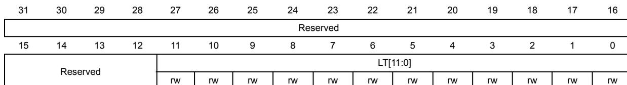
| 31 | 30 | 29 | 28 | 27 | 26 | 25 | 24 | 23 | 22 | 21 | 20 | 19 | 18 | 17 | 16 |
| Reserved | |||||||||||||||
| 15 | 14 | 13 | 12 | 11 | 10 | 9 | 8 | 7 | 6 | 5 | 4 | 3 | 2 | 1 | 0 |
| Reserved | LT[11:0] | ||||||||||||||
| rw | rw | rw | rw | rw | rw | rw | rw | rw | rw | rw | rw | ||||
Bits 31:12 Reserved, must be kept at reset value.
Bits 11:0 LT[11:0] : Analog watchdog lower threshold
These bits are written by software to define the lower threshold for the analog watchdog.
Note: The software can write to these registers when an ADC conversion is ongoing. The programmed value is effective when the next conversion is complete. Writing to this register is performed with a write delay that can create uncertainty on the effective time at which the new value is programmed.
13.13.9 ADC regular sequence register 1 (ADC_SQR1)
Address offset: 0x2C
Reset value: 0x0000 0000
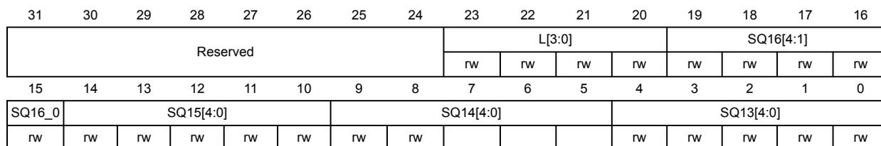
| 31 | 30 | 29 | 28 | 27 | 26 | 25 | 24 | 23 | 22 | 21 | 20 | 19 | 18 | 17 | 16 | ||||
| Reserved | L[3:0] | SQ16[4:1] | |||||||||||||||||
| rw | rw | rw | rw | rw | rw | rw | rw | ||||||||||||
| 15 | 14 | 13 | 12 | 11 | 10 | 9 | 8 | 7 | 6 | 5 | 4 | 3 | 2 | 1 | 0 | ||||
| SQ16_0 | SQ15[4:0] | SQ14[4:0] | SQ13[4:0] | ||||||||||||||||
| rw | rw | rw | rw | rw | rw | rw | rw | rw | rw | rw | rw | rw | |||||||
Bits 31:24 Reserved, must be kept at reset value.
Bits 23:20 L[3:0] : Regular channel sequence length
These bits are written by software to define the total number of conversions in the regular channel conversion sequence.
0000: 1 conversion
0001: 2 conversions
...
1111: 16 conversions
Bits 19:15 SQ16[4:0] : 16th conversion in regular sequence
These bits are written by software with the channel number (0..18) assigned as the 16th in the conversion sequence.
- Bits 14:10 SQ15[4:0] : 15th conversion in regular sequence
- Bits 9:5 SQ14[4:0] : 14th conversion in regular sequence
- Bits 4:0 SQ13[4:0] : 13th conversion in regular sequence
13.13.10 ADC regular sequence register 2 (ADC_SQR2)
Address offset: 0x30
Reset value: 0x0000 0000
| 31 | 30 | 29 | 28 | 27 | 26 | 25 | 24 | 23 | 22 | 21 | 20 | 19 | 18 | 17 | 16 |
|---|---|---|---|---|---|---|---|---|---|---|---|---|---|---|---|
| Reserved | SQ12[4:0] | SQ11[4:0] | SQ10[4:1] | ||||||||||||
| rw | rw | rw | rw | rw | rw | rw | rw | rw | rw | rw | rw | rw | rw | rw | |
| 15 | 14 | 13 | 12 | 11 | 10 | 9 | 8 | 7 | 6 | 5 | 4 | 3 | 2 | 1 | 0 |
| SQ10_0 | SQ9[4:0] | SQ8[4:0] | SQ7[4:0] | ||||||||||||
| rw | rw | rw | rw | rw | rw | rw | rw | rw | rw | rw | rw | rw | rw | rw | |
- Bits 31:30 Reserved, must be kept at reset value.
- Bits 29:26
SQ12[4:0]
: 12th conversion in regular sequence
These bits are written by software with the channel number (0..18) assigned as the 12th in the sequence to be converted. - Bits 24:20 SQ11[4:0] : 11th conversion in regular sequence
- Bits 19:15 SQ10[4:0] : 10th conversion in regular sequence
- Bits 14:10 SQ9[4:0] : 9th conversion in regular sequence
- Bits 9:5 SQ8[4:0] : 8th conversion in regular sequence
- Bits 4:0 SQ7[4:0] : 7th conversion in regular sequence
13.13.11 ADC regular sequence register 3 (ADC_SQR3)
Address offset: 0x34
Reset value: 0x0000 0000
| 31 | 30 | 29 | 28 | 27 | 26 | 25 | 24 | 23 | 22 | 21 | 20 | 19 | 18 | 17 | 16 |
|---|---|---|---|---|---|---|---|---|---|---|---|---|---|---|---|
| Reserved | SQ6[4:0] | SQ5[4:0] | SQ4[4:1] | ||||||||||||
| rw | rw | rw | rw | rw | rw | rw | rw | rw | rw | rw | rw | rw | rw | rw | |
| 15 | 14 | 13 | 12 | 11 | 10 | 9 | 8 | 7 | 6 | 5 | 4 | 3 | 2 | 1 | 0 |
| SQ4_0 | SQ3[4:0] | SQ2[4:0] | SQ1[4:0] | ||||||||||||
| rw | rw | rw | rw | rw | rw | rw | rw | rw | rw | rw | rw | rw | rw | rw | |
- Bits 31:30 Reserved, must be kept at reset value.
- Bits 29:25
SQ6[4:0]
: 6th conversion in regular sequence
These bits are written by software with the channel number (0..18) assigned as the 6th in the sequence to be converted. - Bits 24:20 SQ5[4:0] : 5th conversion in regular sequence
Bits 19:15 SQ4[4:0] : 4th conversion in regular sequence
Bits 14:10 SQ3[4:0] : 3rd conversion in regular sequence
Bits 9:5 SQ2[4:0] : 2nd conversion in regular sequence
Bits 4:0 SQ1[4:0] : 1st conversion in regular sequence
13.13.12 ADC injected sequence register (ADC_JSQR)
Address offset: 0x38
Reset value: 0x0000 0000
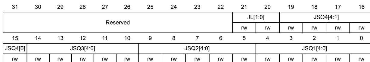
| 31 | 30 | 29 | 28 | 27 | 26 | 25 | 24 | 23 | 22 | 21 | 20 | 19 | 18 | 17 | 16 |
| Reserved | JL[1:0] | JSQ4[4:1] | |||||||||||||
| rw | rw | rw | rw | rw | rw | ||||||||||
| 15 | 14 | 13 | 12 | 11 | 10 | 9 | 8 | 7 | 6 | 5 | 4 | 3 | 2 | 1 | 0 |
| JSQ4[0] | JSQ3[4:0] | JSQ2[4:0] | JSQ1[4:0] | ||||||||||||
| rw | rw | rw | rw | rw | rw | rw | rw | rw | rw | rw | rw | rw | rw | rw | rw |
Bits 31:22 Reserved, must be kept at reset value.
Bits 21:20 JL[1:0] : Injected sequence length
These bits are written by software to define the total number of conversions in the injected channel conversion sequence.
00: 1 conversion
01: 2 conversions
10: 3 conversions
11: 4 conversions
Bits 19:15 JSQ4[4:0] : 4th conversion in injected sequence (when JL[1:0]=3, see note below)
These bits are written by software with the channel number (0..18) assigned as the 4th in the sequence to be converted.
Bits 14:10 JSQ3[4:0] : 3rd conversion in injected sequence (when JL[1:0]=3, see note below)
Bits 9:5 JSQ2[4:0] : 2nd conversion in injected sequence (when JL[1:0]=3, see note below)
Bits 4:0 JSQ1[4:0] : 1st conversion in injected sequence (when JL[1:0]=3, see note below)
Note: When JL[1:0]=3 (4 injected conversions in the sequencer), the ADC converts the channels in the following order: JSQ1[4:0], JSQ2[4:0], JSQ3[4:0], and JSQ4[4:0].
When JL=2 (3 injected conversions in the sequencer), the ADC converts the channels in the following order: JSQ2[4:0], JSQ3[4:0], and JSQ4[4:0].
When JL=1 (2 injected conversions in the sequencer), the ADC converts the channels in starting from JSQ3[4:0], and then JSQ4[4:0].
When JL=0 (1 injected conversion in the sequencer), the ADC converts only JSQ4[4:0] channel.
13.13.13 ADC injected data register x (ADC_JDRx) (x= 1..4)
Address offset: 0x3C - 0x48
Reset value: 0x0000 0000
| 31 | 30 | 29 | 28 | 27 | 26 | 25 | 24 | 23 | 22 | 21 | 20 | 19 | 18 | 17 | 16 |
| Reserved | |||||||||||||||
| 15 | 14 | 13 | 12 | 11 | 10 | 9 | 8 | 7 | 6 | 5 | 4 | 3 | 2 | 1 | 0 |
| JDATA[15:0] | |||||||||||||||
| r | r | r | r | r | r | r | r | r | r | r | r | r | r | r | r |
Bits 31:16 Reserved, must be kept at reset value.
Bits 15:0 JDATA[15:0] : Injected data
These bits are read-only. They contain the conversion result from injected channel x. The data are left -or right-aligned as shown in Figure 48 and Figure 49 .
13.13.14 ADC regular data register (ADC_DR)
Address offset: 0x4C
Reset value: 0x0000 0000
| 31 | 30 | 29 | 28 | 27 | 26 | 25 | 24 | 23 | 22 | 21 | 20 | 19 | 18 | 17 | 16 |
| Reserved | |||||||||||||||
| 15 | 14 | 13 | 12 | 11 | 10 | 9 | 8 | 7 | 6 | 5 | 4 | 3 | 2 | 1 | 0 |
| DATA[15:0] | |||||||||||||||
| r | r | r | r | r | r | r | r | r | r | r | r | r | r | r | r |
Bits 31:16 Reserved, must be kept at reset value.
Bits 15:0 DATA[15:0] : Regular data
These bits are read-only. They contain the conversion result from the regular channels. The data are left- or right-aligned as shown in Figure 48 and Figure 49 .
13.13.15 ADC Common status register (ADC_CSR)
Address offset: 0x00 (this offset address is relative to ADC1 base address + 0x300)
Reset value: 0x0000 0000
This register provides an image of the status bits of the different ADCs. Nevertheless it is read-only and does not allow to clear the different status bits. Instead each status bit must be cleared by writing it to 0 in the corresponding ADC_SR register.
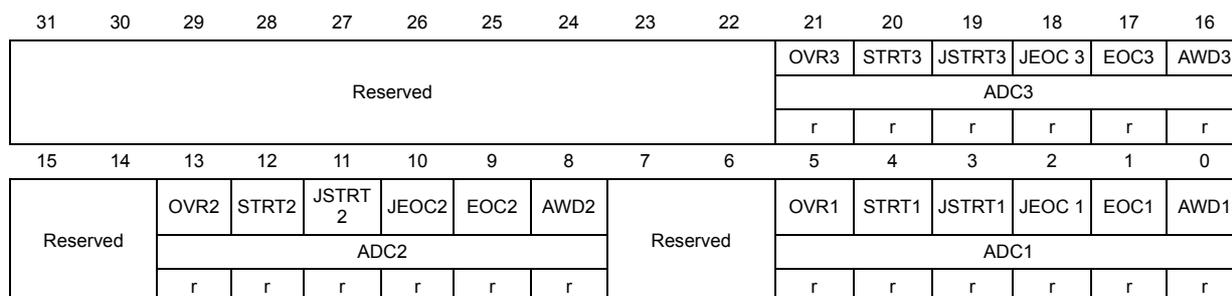
| 31 | 30 | 29 | 28 | 27 | 26 | 25 | 24 | 23 | 22 | 21 | 20 | 19 | 18 | 17 | 16 |
|---|---|---|---|---|---|---|---|---|---|---|---|---|---|---|---|
| Reserved | OVR3 | STRT3 | JSTRT3 | JEOC3 | EOC3 | AWD3 | |||||||||
| ADC3 | |||||||||||||||
| Reserved | r | r | r | r | r | r | |||||||||
| 15 | 14 | 13 | 12 | 11 | 10 | 9 | 8 | 7 | 6 | 5 | 4 | 3 | 2 | 1 | 0 |
| Reserved | OVR2 | STRT2 | JSTRT2 | JEOC2 | EOC2 | AWD2 | Reserved | OVR1 | STRT1 | JSTRT1 | JEOC1 | EOC1 | AWD1 | ||
| ADC2 | ADC1 | ||||||||||||||
| Reserved | r | r | r | r | r | r | Reserved | r | r | r | r | r | r | ||
Bits 31:22 Reserved, must be kept at reset value.
Bit 21 OVR3 : Overrun flag of ADC3
This bit is a copy of the OVR bit in the ADC3_SR register.
Bit 20 STRT3 : Regular channel Start flag of ADC3
This bit is a copy of the STRT bit in the ADC3_SR register.
Bit 19 JSTRT3 : Injected channel Start flag of ADC3
This bit is a copy of the JSTRT bit in the ADC3_SR register.
Bit 18 JEOC3 : Injected channel end of conversion of ADC3
This bit is a copy of the JEOC bit in the ADC3_SR register.
Bit 17 EOC3 : End of conversion of ADC3
This bit is a copy of the EOC bit in the ADC3_SR register.
Bit 16 AWD3 : Analog watchdog flag of ADC3
This bit is a copy of the AWD bit in the ADC3_SR register.
Bits 15:14 Reserved, must be kept at reset value.
Bit 13 OVR2 : Overrun flag of ADC2
This bit is a copy of the OVR bit in the ADC2_SR register.
Bit 12 STRT2 : Regular channel Start flag of ADC2
This bit is a copy of the STRT bit in the ADC2_SR register.
Bit 11 JSTRT2 : Injected channel Start flag of ADC2
This bit is a copy of the JSTRT bit in the ADC2_SR register.
Bit 10 JEOC2 : Injected channel end of conversion of ADC2
This bit is a copy of the JEOC bit in the ADC2_SR register.
Bit 9 EOC2 : End of conversion of ADC2
This bit is a copy of the EOC bit in the ADC2_SR register.
Bit 8 AWD2 : Analog watchdog flag of ADC2
This bit is a copy of the AWD bit in the ADC2_SR register.
- Bits 7:6 Reserved, must be kept at reset value.
- Bit 5
OVR1
: Overrun flag of ADC1
This bit is a copy of the OVR bit in the ADC1_SR register. - Bit 4
STRT1
: Regular channel Start flag of ADC1
This bit is a copy of the STRT bit in the ADC1_SR register. - Bit 3
JSTRT1
: Injected channel Start flag of ADC1
This bit is a copy of the JSTRT bit in the ADC1_SR register. - Bit 2
JEOC1
: Injected channel end of conversion of ADC1
This bit is a copy of the JEOC bit in the ADC1_SR register. - Bit 1
EOC1
: End of conversion of ADC1
This bit is a copy of the EOC bit in the ADC1_SR register. - Bit 0
AWD1
: Analog watchdog flag of ADC1
This bit is a copy of the AWD bit in the ADC1_SR register.
13.13.16 ADC common control register (ADC_CCR)
Address offset: 0x04 (this offset address is relative to ADC1 base address + 0x300)
Reset value: 0x0000 0000
| 31 | 30 | 29 | 28 | 27 | 26 | 25 | 24 | 23 | 22 | 21 | 20 | 19 | 18 | 17 | 16 |
|---|---|---|---|---|---|---|---|---|---|---|---|---|---|---|---|
| Reserved | TSVREFE | VBATE | Reserved | ADCPRE | |||||||||||
| rw | rw | rw | rw | ||||||||||||
| 15 | 14 | 13 | 12 | 11 | 10 | 9 | 8 | 7 | 6 | 5 | 4 | 3 | 2 | 1 | 0 |
| DMA[1:0] | DDS | Res. | DELAY[3:0] | Reserved | MULTI[4:0] | ||||||||||
| rw | rw | rw | rw | rw | rw | rw | rw | rw | rw | rw | rw | ||||
- Bits 31:24 Reserved, must be kept at reset value.
- Bit 23
TSVREFE
: Temperature sensor and V
REFINT
enable
This bit is set and cleared by software to enable/disable the temperature sensor and the V REFINT channel.- 0: Temperature sensor and V REFINT channel disabled
- 1: Temperature sensor and V REFINT channel enabled
- Bit 22
VBATE
: V
BAT
enable
This bit is set and cleared by software to enable/disable the V BAT channel.- 0: V BAT channel disabled
- 1: V BAT channel enabled
- Bits 21:18 Reserved, must be kept at reset value.
Bits 17:16 ADCPRE : ADC prescaler
Set and cleared by software to select the frequency of the clock to the ADC. The clock is common for all the ADCs.
Note: 00: PCLK2 divided by 2
01: PCLK2 divided by 4
10: PCLK2 divided by 6
11: PCLK2 divided by 8
Bits 15:14 DMA : Direct memory access mode for multi ADC mode
This bit-field is set and cleared by software. Refer to the DMA controller section for more details.
00: DMA mode disabled
01: DMA mode 1 enabled (2 / 3 half-words one by one - 1 then 2 then 3)
10: DMA mode 2 enabled (2 / 3 half-words by pairs - 2&1 then 1&3 then 3&2)
11: DMA mode 3 enabled (2 / 3 bytes by pairs - 2&1 then 1&3 then 3&2)
Bit 13 DDS : DMA disable selection (for multi-ADC mode)
This bit is set and cleared by software.
0: No new DMA request is issued after the last transfer (as configured in the DMA controller). DMA bits are not cleared by hardware, however they must have been cleared and set to the wanted mode by software before new DMA requests can be generated.
1: DMA requests are issued as long as data are converted and DMA = 01, 10 or 11.
Bit 12 Reserved, must be kept at reset value.
Bit 11:8 DELAY: Delay between 2 sampling phases
Set and cleared by software. These bits are used in dual or triple interleaved modes.
0000: \( 5 \cdot T_{ADCCLK} \)
0001: \( 6 \cdot T_{ADCCLK} \)
0010: \( 7 \cdot T_{ADCCLK} \)
...
1111: \( 20 \cdot T_{ADCCLK} \)
Bits 7:5 Reserved, must be kept at reset value.
Bits 4:0 MULTI[4:0]: Multi ADC mode selection
These bits are written by software to select the operating mode.
– All the ADCs independent:
00000: Independent mode
– 00001 to 01001: Dual mode, ADC1 and ADC2 working together, ADC3 is independent
00001: Combined regular simultaneous + injected simultaneous mode
00010: Combined regular simultaneous + alternate trigger mode
00011: Reserved
00101: Injected simultaneous mode only
00110: Regular simultaneous mode only
00111: interleaved mode only
01001: Alternate trigger mode only
– 10001 to 11001: Triple mode: ADC1, 2 and 3 working together
10001: Combined regular simultaneous + injected simultaneous mode
10010: Combined regular simultaneous + alternate trigger mode
10011: Reserved
10101: Injected simultaneous mode only
10110: Regular simultaneous mode only
10111: interleaved mode only
11001: Alternate trigger mode only
All other combinations are reserved and must not be programmed
Note: In multi mode, a change of channel configuration generates an abort that can cause a loss of synchronization. It is recommended to disable the multi ADC mode before any configuration change.
13.13.17 ADC common regular data register for dual and triple modes (ADC_CDR)
Address offset: 0x08 (this offset address is relative to ADC1 base address + 0x300)
Reset value: 0x0000 0000
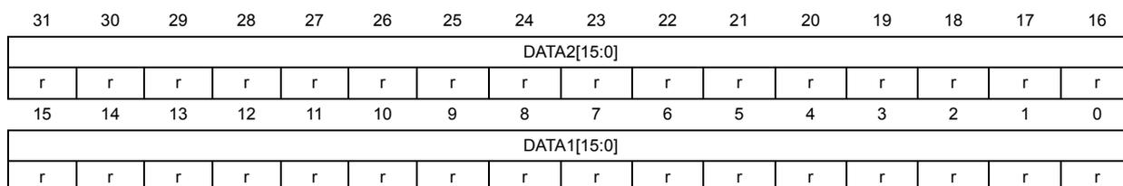
| 31 | 30 | 29 | 28 | 27 | 26 | 25 | 24 | 23 | 22 | 21 | 20 | 19 | 18 | 17 | 16 |
| DATA2[15:0] | |||||||||||||||
| r | r | r | r | r | r | r | r | r | r | r | r | r | r | r | r |
| 15 | 14 | 13 | 12 | 11 | 10 | 9 | 8 | 7 | 6 | 5 | 4 | 3 | 2 | 1 | 0 |
| DATA1[15:0] | |||||||||||||||
| r | r | r | r | r | r | r | r | r | r | r | r | r | r | r | r |
Bits 31:16 DATA2[15:0] : 2nd data item of a pair of regular conversions
- – In dual mode, these bits contain the regular data of ADC2. Refer to Dual ADC mode .
- – In triple mode, these bits contain alternatively the regular data of ADC2, ADC1 and ADC3. Refer to Triple ADC mode .
Bits 15:0 DATA1[15:0] : 1st data item of a pair of regular conversions
- – In dual mode, these bits contain the regular data of ADC1. Refer to Dual ADC mode
- – In triple mode, these bits contain alternatively the regular data of ADC1, ADC3 and ADC2. Refer to Triple ADC mode .
13.13.18 ADC register map
The following table summarizes the ADC registers.
Table 72. ADC global register map
| Offset | Register |
|---|---|
| 0x000 - 0x04C | ADC1 |
| 0x050 - 0x0FC | Reserved |
| 0x100 - 0x14C | ADC2 |
| 0x118 - 0x1FC | Reserved |
| 0x200 - 0x24C | ADC3 |
| 0x250 - 0x2FC | Reserved |
| 0x300 - 0x308 | Common registers |
Table 73. ADC register map and reset values for each ADC
| Offset | Register | 31 | 30 | 29 | 28 | 27 | 26 | 25 | 24 | 23 | 22 | 21 | 20 | 19 | 18 | 17 | 16 | 15 | 14 | 13 | 12 | 11 | 10 | 9 | 8 | 7 | 6 | 5 | 4 | 3 | 2 | 1 | 0 | |
|---|---|---|---|---|---|---|---|---|---|---|---|---|---|---|---|---|---|---|---|---|---|---|---|---|---|---|---|---|---|---|---|---|---|---|
| 0x00 | ADC_SR | Reserved | OVR | STRT | JSTRT | JEOC | EOC | AWD | ||||||||||||||||||||||||||
| Reset value | 0 | 0 | 0 | 0 | 0 | 0 | ||||||||||||||||||||||||||||
| 0x04 | ADC_CR1 | Reserved | OVRIE | RES[1:0] | AWDEN | JAWDEN | Reserved | DISC NUM [2:0] | JDISCEN | DISCEN | JAUTO | AWDSGL | SCAN | JEOCIE | AWDIE | EOCIE | AWDCH[4:0] | |||||||||||||||||
| Reset value | 0 | 0 | 0 | 0 | 0 | 0 | 0 | 0 | 0 | 0 | 0 | 0 | 0 | 0 | 0 | 0 | 0 | 0 | 0 | 0 | 0 | |||||||||||||
| 0x08 | ADC_CR2 | Reserved | SWSTART | EXTEN[1:0] | EXTSEL [3:0] | Reserved | JSWSTART | JEXTEN[1:0] | JEXTSEL [3:0] | Reserved | ALIGN | EOCS | DDS | DMA | Reserved | CONT | ADON | |||||||||||||||||
| Reset value | 0 | 0 | 0 | 0 | 0 | 0 | 0 | 0 | 0 | 0 | 0 | 0 | 0 | 0 | 0 | 0 | 0 | 0 | 0 | |||||||||||||||
| 0x0C | ADC_SMPR1 | Sample time bits SMPx_x | ||||||||||||||||||||||||||||||||
| Reset value | 0 | 0 | 0 | 0 | 0 | 0 | 0 | 0 | 0 | 0 | 0 | 0 | 0 | 0 | 0 | 0 | 0 | 0 | 0 | 0 | 0 | 0 | 0 | 0 | 0 | 0 | 0 | 0 | 0 | 0 | 0 | 0 | ||
| 0x10 | ADC_SMPR2 | Sample time bits SMPx_x | ||||||||||||||||||||||||||||||||
| Reset value | 0 | 0 | 0 | 0 | 0 | 0 | 0 | 0 | 0 | 0 | 0 | 0 | 0 | 0 | 0 | 0 | 0 | 0 | 0 | 0 | 0 | 0 | 0 | 0 | 0 | 0 | 0 | 0 | 0 | 0 | 0 | 0 | ||
| 0x14 | ADC_JOFR1 | Reserved | JOFFSET1[11:0] | |||||||||||||||||||||||||||||||
| Reset value | 0 | 0 | 0 | 0 | 0 | 0 | 0 | 0 | 0 | 0 | 0 | 0 | ||||||||||||||||||||||
| 0x18 | ADC_JOFR2 | Reserved | JOFFSET2[11:0] | |||||||||||||||||||||||||||||||
| Reset value | 0 | 0 | 0 | 0 | 0 | 0 | 0 | 0 | 0 | 0 | 0 | 0 | ||||||||||||||||||||||
| 0x1C | ADC_JOFR3 | Reserved | JOFFSET3[11:0] | |||||||||||||||||||||||||||||||
| Reset value | 0 | 0 | 0 | 0 | 0 | 0 | 0 | 0 | 0 | 0 | 0 | 0 | ||||||||||||||||||||||
| 0x20 | ADC_JOFR4 | Reserved | JOFFSET4[11:0] | |||||||||||||||||||||||||||||||
| Reset value | 0 | 0 | 0 | 0 | 0 | 0 | 0 | 0 | 0 | 0 | 0 | 0 | ||||||||||||||||||||||
| 0x24 | ADC_HTR | Reserved | HT[11:0] | |||||||||||||||||||||||||||||||
| Reset value | 1 | 1 | 1 | 1 | 1 | 1 | 1 | 1 | 1 | 1 | 1 | 1 | ||||||||||||||||||||||
| 0x28 | ADC_LTR | Reserved | LT[11:0] | |||||||||||||||||||||||||||||||
| Reset value | 0 | 0 | 0 | 0 | 0 | 0 | 0 | 0 | 0 | 0 | 0 | 0 | ||||||||||||||||||||||
| 0x2C | ADC_SQR1 | Reserved | L[3:0] | Regular channel sequence SQx_x bits | ||||||||||||||||||||||||||||||
| Reset value | 0 | 0 | 0 | 0 | 0 | 0 | 0 | 0 | 0 | 0 | 0 | 0 | 0 | 0 | 0 | 0 | 0 | 0 | 0 | 0 | ||||||||||||||
| 0x30 | ADC_SQR2 | Reserved | Reserved | Regular channel sequence SQx_x bits | ||||||||||||||||||||||||||||||
| Reset value | 0 | 0 | 0 | 0 | 0 | 0 | 0 | 0 | 0 | 0 | 0 | 0 | 0 | 0 | 0 | 0 | 0 | 0 | 0 | 0 | 0 | 0 | 0 | 0 | 0 | 0 | 0 | 0 | 0 | 0 | ||||
| 0x34 | ADC_SQR3 | Reserved | Regular channel sequence SQx_x bits | |||||||||||||||||||||||||||||||
| Reset value | 0 | 0 | 0 | 0 | 0 | 0 | 0 | 0 | 0 | 0 | 0 | 0 | 0 | 0 | 0 | 0 | 0 | 0 | 0 | 0 | 0 | 0 | 0 | 0 | 0 | 0 | 0 | |||||||
| 0x38 | ADC_JSQR | Reserved | JL[1:0] | Injected channel sequence JSQx_x bits | ||||||||||||||||||||||||||||||
| Reset value | 0 | 0 | 0 | 0 | 0 | 0 | 0 | 0 | 0 | 0 | 0 | 0 | 0 | 0 | 0 | 0 | 0 | 0 | 0 | 0 | 0 | 0 | ||||||||||||
| 0x3C | ADC_JDR1 | Reserved | JDATA[15:0] | |||||||||||||||||||||||||||||||
| Reset value | 0 | 0 | 0 | 0 | 0 | 0 | 0 | 0 | 0 | 0 | 0 | 0 | 0 | 0 | 0 | 0 | ||||||||||||||||||
| 0x40 | ADC_JDR2 | Reserved | JDATA[15:0] | |||||||||||||||||||||||||||||||
| Reset value | 0 | 0 | 0 | 0 | 0 | 0 | 0 | 0 | 0 | 0 | 0 | 0 | 0 | 0 | 0 | 0 | ||||||||||||||||||
| 0x44 | ADC_JDR3 | Reserved | JDATA[15:0] | |||||||||||||||||||||||||||||||
| Reset value | 0 | 0 | 0 | 0 | 0 | 0 | 0 | 0 | 0 | 0 | 0 | 0 | 0 | 0 | 0 | 0 | ||||||||||||||||||
| 0x48 | ADC_JDR4 | Reserved | JDATA[15:0] | |||||||||||||||||||||||||||||||
| Reset value | 0 | 0 | 0 | 0 | 0 | 0 | 0 | 0 | 0 | 0 | 0 | 0 | 0 | 0 | 0 | 0 | ||||||||||||||||||
| 0x4C | ADC_DR | Reserved | Regular DATA[15:0] | |||||||||||||||||||||||||||||||
| Reset value | 0 | 0 | 0 | 0 | 0 | 0 | 0 | 0 | 0 | 0 | 0 | 0 | 0 | 0 | 0 | 0 | ||||||||||||||||||
Table 74. ADC register map and reset values (common ADC registers)
| Offset | Register | 31 | 30 | 29 | 28 | 27 | 26 | 25 | 24 | 23 | 22 | 21 | 20 | 19 | 18 | 17 | 16 | 15 | 14 | 13 | 12 | 11 | 10 | 9 | 8 | 7 | 6 | 5 | 4 | 3 | 2 | 1 | 0 | |
|---|---|---|---|---|---|---|---|---|---|---|---|---|---|---|---|---|---|---|---|---|---|---|---|---|---|---|---|---|---|---|---|---|---|---|
| 0x00 | ADC_CSR | Reserved | OVR | STRT | JSTRT | JEOC | EOC | AWD | Reserved | OVR | STRT | JSTRT | JEOC | EOC | AWD | Reserved | OVR | STRT | JSTRT | JEOC | EOC | AWD | ||||||||||||
| Reset value | 0 | 0 | 0 | 0 | 0 | 0 | 0 | 0 | 0 | 0 | 0 | 0 | 0 | 0 | 0 | 0 | 0 | 0 | ||||||||||||||||
| 0x04 | ADC_CCR | Reserved | ADC3 | ADC2 | ADC1 | Reserved | DELAY [3:0] | Reserved | MULTI [4:0] | |||||||||||||||||||||||||
| Reset value | ||||||||||||||||||||||||||||||||||
| 0x08 | ADC_CDR | Regular DATA2[15:0] | Regular DATA1[15:0] | |||||||||||||||||||||||||||||||
| Reset value | 0 | 0 | 0 | 0 | 0 | 0 | 0 | 0 | 0 | 0 | 0 | 0 | 0 | 0 | 0 | 0 | 0 | 0 | 0 | 0 | 0 | 0 | 0 | 0 | 0 | 0 | 0 | 0 | 0 | 0 | 0 | 0 | ||
Refer to Section 2.3: Memory map for the register boundary addresses.