11. Chrom-Art Accelerator™ controller (DMA2D)
11.1 DMA2D introduction
The Chrom-Art Accelerator™ (DMA2D) is a specialized DMA dedicated to image manipulation. It can perform the following operations:
- • Filling a part or the whole of a destination image with a specific color
- • Copying a part or the whole of a source image into a part or the whole of a destination image
- • Copying a part or the whole of a source image into a part or the whole of a destination image with a pixel format conversion
- • Blending a part and/or two complete source images with different pixel format and copy the result into a part or the whole of a destination image with a different color format.
All the classical color coding schemes are supported from 4-bit up to 32-bit per pixel with indexed or direct color mode. The DMA2D has its own dedicated memories for CLUTs (color look-up tables).
11.2 DMA2D main features
The main DMA2D features are:
- • Single AHB master bus architecture.
- • AHB slave programming interface supporting 8/16/32-bit accesses (except for CLUT accesses which are 32-bit).
- • User programmable working area size
- • User programmable offset for sources and destination areas
- • User programmable sources and destination addresses on the whole memory space
- • Up to 2 sources with blending operation
- • Alpha value can be modified (source value, fixed value or modulated value)
- • User programmable source and destination color format
- • Up to 11 color formats supported from 4-bit up to 32-bit per pixel with indirect or direct color coding
- • 2 internal memories for CLUT storage in indirect color mode
- • Automatic CLUT loading or CLUT programming via the CPU
- • User programmable CLUT size
- • Internal timer to control AHB bandwidth
- • 4 operating modes: register-to-memory, memory-to-memory, memory-to-memory with pixel format conversion, and memory-to-memory with pixel format conversion and blending
- • Area filling with a fixed color
- • Copy from an area to another
- • Copy with pixel format conversion between source and destination images
- • Copy from two sources with independent color format and blending
- • Abort and suspend of DMA2D operations
- • Watermark interrupt on a user programmable destination line
- • Interrupt generation on bus error or access conflict
- • Interrupt generation on process completion
11.3 DMA2D functional description
11.3.1 General description
The DMA2D controller performs direct memory transfer. As an AHB master, it can take the control of the AHB bus matrix to initiate AHB transactions.
The DMA2D can operate in the following modes:
- • Register-to-memory
- • Memory-to-memory
- • Memory-to-memory with Pixel Format Conversion
- • Memory-to-memory with Pixel Format Conversion and Blending
The AHB slave port is used to program the DMA2D controller.
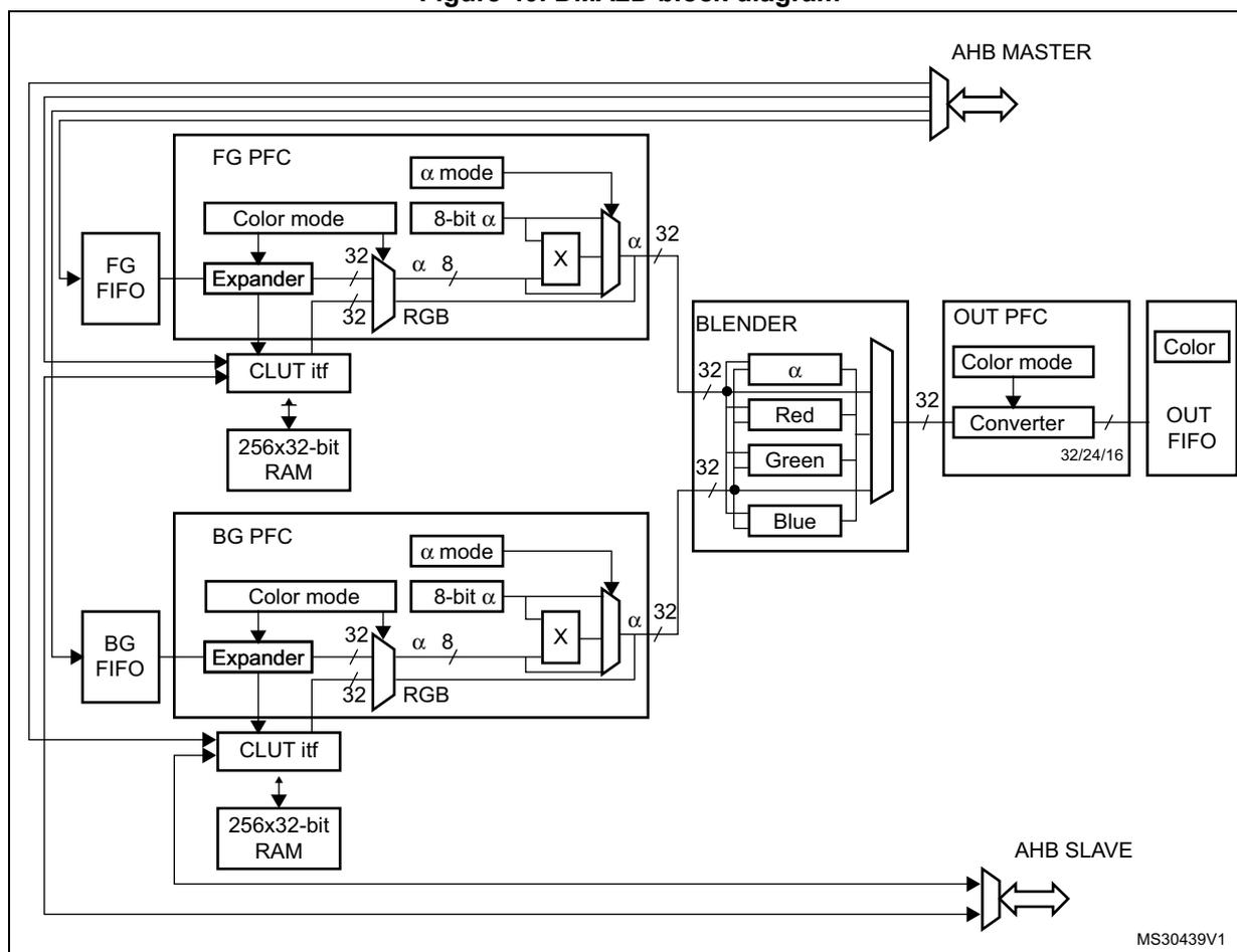
The block diagram of the DMA2D is shown in Figure 40: DMA2D block diagram .
Figure 40. DMA2D block diagram
11.3.2 DMA2D control
The DMA2D controller is configured through the DMA2D Control Register (DMA2D_CR) which allows selecting:
The user application can perform the following operations:
- • Select the operating mode
- • Enable/disable the DMA2D interrupt
- • Start/suspend/abort ongoing data transfers
11.3.3 DMA2D foreground and background FIFOs
The DMA2D foreground (FG) FG FIFO and background (BG) FIFO fetch the input data to be copied and/or processed.
The FIFOs fetch the pixels according to the color format defined in their respective pixel format converter (PFC).
They are programmed through a set of control registers:
- • DMA2D foreground memory address register (DMA2D_FGMAR)
- • DMA2D foreground offset register (DMA2D_FGOR)
- • DMA2D background memory address register (DMA2D_BGMAR)
- • DMA2D background offset register (DMA2D_BGBOR)
- • DMA2D number of lines register (number of lines and pixel per lines) (DMA2D_NLR)
When the DMA2D operates in register-to-memory mode, none of the FIFOs is activated.
When the DMA2D operates in memory-to-memory mode (no pixel format conversion nor blending operation), only the FG FIFO is activated and acts as a buffer.
When the DMA2D operates in memory-to-memory operation with pixel format conversion (no blending operation), the BG FIFO is not activated.
11.3.4 DMA2D foreground and background pixel format converter (PFC)
DMA2D foreground pixel format converter (PFC) and background pixel format converter perform the pixel format conversion to generate a 32-bit per pixel value. The PFC can also modify the alpha channel.
The first stage of the converter converts the color format. The original color format of the foreground pixel and background pixels are configured through the CM[3:0] bits of the DMA2D_FGPFCCR and DMA2D_BGPFCCR, respectively.
The supported input formats are given in Table 53: Supported color mode in input .
Table 53. Supported color mode in input
| CM[3:0] | Color mode |
|---|---|
| 0000 | ARGB8888 |
| 0001 | RGB888 |
| 0010 | RGB565 |
| 0011 | ARGB1555 |
| 0100 | ARGB4444 |
| 0101 | L8 |
| 0110 | AL44 |
| 0111 | AL88 |
| 1000 | L4 |
| 1001 | A8 |
| 1010 | A4 |
The color format are coded as follows:
- • Alpha value field: transparency
0xFF value corresponds to an opaque pixel and 0x00 to a transparent one. - • R field for Red
- • G field for Green
- • B field for Blue
- • L field: luminance
This field is the index to a CLUT to retrieve the three/four RGB/ARGB components.
If the original format was direct color mode, then the extension to 8-bit per channel is performed by copying the MSBs into the LSBs. This ensures a perfect linearity of the conversion.
If the original format does not include an alpha channel, the alpha value is automatically set to 0xFF (opaque).
If the original format is indirect color mode, a CLUT is required and each pixel format converter is associated with a 256 entry 32-bit CLUT.
For the specific alpha mode A4 and A8, no color information is stored nor indexed. The color to be used for the image generation is fixed and is defined in the DMA2D_FGCOLR for foreground pixels and in the DMA2D_BGCOLR register for background pixels.
The order of the fields in the system memory is defined in Table 54: Data order in memory .
Table 54. Data order in memory
| Color Mode | @ + 3 | @ + 2 | @ + 1 | @ + 0 |
|---|---|---|---|---|
| ARGB8888 | A 0 [7:0] | R 0 [7:0] | G 0 [7:0] | B 0 [7:0] |
| RGB888 | B 1 [7:0] | R 0 [7:0] | G 0 [7:0] | B 0 [7:0] |
| G 2 [7:0] | B 2 [7:0] | R 1 [7:0] | G 1 [7:0] | |
| R 3 [7:0] | G 3 [7:0] | B 3 [7:0] | R 2 [7:0] | |
| RGB565 | R 1 [4:0]G 1 [5:3] | G 1 [2:0]B 1 [4:0] | R 0 [4:0]G 0 [5:3] | G 0 [2:0]B 0 [4:0] |
| ARGB1555 | A 1 [0]R 1 [4:0]G 1 [4:3] | G 1 [2:0]B 1 [4:0] | A 0 [0]R 0 [4:0]G 0 [4:3] | G 0 [2:0]B 0 [4:0] |
| ARGB4444 | A 1 [3:0]R 1 [3:0] | G 1 [3:0]B 1 [3:0] | A 0 [3:0]R 0 [3:0] | G 0 [3:0]B 0 [3:0] |
| L8 | L 3 [7:0] | L 2 [7:0] | L 1 [7:0] | L 0 [7:0] |
| AL44 | A 3 [3:0]L 3 [3:0] | A 2 [3:0]L 2 [3:0] | A 1 [3:0]L 1 [3:0] | A 0 [3:0]L 0 [3:0] |
| AL88 | A 1 [7:0] | L 1 [7:0] | A 0 [7:0] | L 0 [7:0] |
| L4 | L 7 [3:0]L 6 [3:0] | L 5 [3:0]L 4 [3:0] | L 3 [3:0]L 2 [3:0] | L 1 [3:0]L 0 [3:0] |
| A8 | A 3 [7:0] | A 2 [7:0] | A 1 [7:0] | A 0 [7:0] |
| A4 | A 7 [3:0]A 6 [3:0] | A 5 [3:0]A 4 [3:0] | A 3 [3:0]A 2 [3:0] | A 1 [3:0]A 0 [3:0] |
The 24-bit RGB888 aligned on 32-bit is supported through the ARGB8888 mode.
Once the 32-bit value is generated, the alpha channel can be modified according to the AM[1:0] field of the DMA2D_FGPFCCR/DMA2D_BGPFCCR registers as shown in Table 55: Alpha mode configuration .
The alpha channel can be:
- • kept as it is (no modification),
- • replaced by the ALPHA[7:0] value of DMA2D_FGPFCCR/DMA2D_BGPFCCR,
- • or replaced by the original alpha value multiplied by the ALPHA[7:0] value of DMA2D_FGPFCCR/DMA2D_BGPFCCR divided by 255.
Table 55. Alpha mode configuration
| AM[1:0] | Alpha mode |
|---|---|
| 00 | No modification |
| 01 | Replaced by value in DMA2D_xxPFCCR |
| 10 | Replaced by original value multiplied by the value in DMA2D_xxPFCCR / 255 |
| 11 | Reserved |
11.3.5 DMA2D foreground and background CLUT interface
The CLUT interface manages the CLUT memory access and the automatic loading of the CLUT.
Three kinds of accesses are possible:
- • CLUT read by the PFC during pixel format conversion operation
- • CLUT accessed through the AHB slave port when the CPU is reading or writing data into the CLUT
- • CLUT written through the AHB master port when an automatic loading of the CLUT is performed
The CLUT memory loading can be done in two different ways:
- • Automatic loading
The following sequence should be followed to load the CLUT:
- a) Program the CLUT address into the DMA2D_FGCMAR register (foreground CLUT) or DMA2D_BGCMAR register (background CLUT)
- b) Program the CLUT size in the CS[7:0] field of the DMA2D_FGPFCCR register (foreground CLUT) or DMA2D_BGPFCCR register (background CLUT).
- c) Set the START bit of the DMA2D_FGPFCCR register (foreground CLUT) or DMA2D_BGPFCCR register (background CLUT) to start the transfer. During this automatic loading process, the CLUT is not accessible by the CPU. If a conflict occurs, a CLUT access error interrupt is raised assuming CAEIE is set to '1' in DMA2D_CR.
- • Manual loading
The application has to program the CLUT manually through the DMA2D AHB slave port to which the local CLUT memory is mapped. The foreground CLUT is located at address offset 0x0400 and the background CLUT at address offset 0x0800.
The CLUT format can be 24 or 32 bits. It is configured through the CCM bit of the DMA2D_FGPFCCR register (foreground CLUT) or DMA2D_BGPFCCR register (background CLUT) as shown in Table 56: Supported CLUT color mode .
Table 56. Supported CLUT color mode
| CCM | CLUT color mode |
|---|---|
| 0 | 32-bit ARGB8888 |
| 1 | 24-bit RGB888 |
The way the CLUT data are organized in the system memory is specified in Table 57: CLUT data order in memory .
Table 57. CLUT data order in memory
| CLUT Color Mode | @ + 3 | @ + 2 | @ + 1 | @ + 0 |
|---|---|---|---|---|
| ARGB8888 | A 0 [7:0] | R 0 [7:0] | G 0 [7:0] | B 0 [7:0] |
| RGB888 | B 1 [7:0] | R 0 [7:0] | G 0 [7:0] | B 0 [7:0] |
| G 2 [7:0] | B 2 [7:0] | R 1 [7:0] | G 1 [7:0] | |
| R 3 [7:0] | G 3 [7:0] | B 3 [7:0] | R 2 [7:0] |
11.3.6 DMA2D blender
The DMA2D blender blends the source pixels by pair to compute the resulting pixel.
The blending is performed according to the following equation:
Division is rounded to the nearest lower integer
No configuration register is required by the blender. The blender usage depends on the DMA2D operating mode defined in MODE[1:0] field of the DMA2D_CR register.
11.3.7 DMA2D output PFC
The output PFC performs the pixel format conversion from 32 bits to the output format defined in the CM[2:0] field of the DMA2D output pixel format converter configuration register (DMA2D_OPFCCR).
The supported output formats are given in Table 58: Supported color mode in output
Table 58. Supported color mode in output
| CM[2:0] | Color mode |
|---|---|
| 000 | ARGB8888 |
| 001 | RGB888 |
| 010 | RGB565 |
| 011 | ARGB1555 |
| 100 | ARGB4444 |
11.3.8 DMA2D output FIFO
The output FIFO programs the pixels according to the color format defined in the output PFC.
The destination area is defined through a set of control registers:
- • DMA2D output memory address register (DMA2D_OMAR)
- • DMA2D output offset register (DMA2D_OOR)
- • DMA2D number of lines register (number of lines and pixel per lines) (DMA2D_NLR)
If the DMA2D operates in register-to-memory mode, the configured output rectangle is filled by the color specified in the DMA2D output color register (DMA2D_OCOLR) which contains a fixed 32-bit, 24-bit or 16-bit value. The format is selected by the CM[2:0] field of the DMA2D_OPFCCR register.
The data are stored into the memory in the order defined in Table 59: Data order in memory
Table 59. Data order in memory
| Color Mode | @ + 3 | @ + 2 | @ + 1 | @ + 0 |
|---|---|---|---|---|
| ARGB8888 | A 0 [7:0] | R 0 [7:0] | G 0 [7:0] | B 0 [7:0] |
| RGB888 | B 1 [7:0] | R 0 [7:0] | G 0 [7:0] | B 0 [7:0] |
| G 2 [7:0] | B 2 [7:0] | R 1 [7:0] | G 1 [7:0] | |
| R 3 [7:0] | G 3 [7:0] | B 3 [7:0] | R 2 [7:0] | |
| RGB565 | R 1 [4:0]G 1 [5:3] | G 1 [2:0]B 1 [4:0] | R 0 [4:0]G 0 [5:3] | G 0 [2:0]B 0 [4:0] |
| ARGB1555 | A 1 [0]R 1 [4:0]G 1 [4:3] | G 1 [2:0]B 1 [4:0] | A 0 [0]R 0 [4:0]G 0 [4:3] | G 0 [2:0]B 0 [4:0] |
| ARGB4444 | A 1 [3:0]R 1 [3:0] | G 1 [3:0]B 1 [3:0] | A 0 [3:0]R 0 [3:0] | G 0 [3:0]B 0 [3:0] |
The RGB888 aligned on 32-bit is supported through the ARGB8888 mode.
11.3.9 DMA2D AHB master port timer
An 8-bit timer is embedded into the AHB master port to provide an optional limitation of the bandwidth on the crossbar.
This timer is clocked by the AHB clock and counts a dead time between two consecutive accesses. This limits the bandwidth usage.
The timer enabling and the dead time value are configured through the AHB master port timer configuration register (DMA2D_AMPTCR).
11.3.10 DMA2D transactions
DMA2D transactions consist of a sequence of a given number of data transfers. The number of data and the width can be programmed by software.
Each DMA2D data transfer is composed of up to 4 steps:
- 1. Data loading from the memory location pointed by the DMA2D_FGMAR register and pixel format conversion as defined in DMA2D_FGCR.
- 2. Data loading from a memory location pointed by the DMA2D_BGMAR register and pixel format conversion as defined in DMA2D_BGCR.
- 3. Blending of all retrieved pixels according to the alpha channels resulting of the PFC operation on alpha values.
- 4. Pixel format conversion of the resulting pixels according to the DMA2D_OCR register and programming of the data to the memory location addressed through the DMA2D_OMAR register.
11.3.11 DMA2D configuration
Both source and destination data transfers can target peripherals and memories in the whole 4 Gbyte memory area, at addresses ranging between 0x0000 0000 and 0xFFFF FFFF.
The DMA2D can operate in any of the four following modes selected through MODE[1:0] bits of the DMA2D_CR register:
- • Register-to-memory
- • Memory-to-memory
- • Memory-to-memory with PFC
- • Memory-to-memory with PFC and blending
Register-to-memory
The register-to-memory mode is used to fill a user defined area with a predefined color.
The color format is set in the DMA2D_OPFCCR.
The DMA2D does not perform any data fetching from any source. It just writes the color defined in the DMA2D_OCOLR register to the area located at the address pointed by the DMA2D_OMAR and defined in the DMA2D_NLR and DMA2D_OOR.
Memory-to-memory
In memory-to-memory mode, the DMA2D does not perform any graphical data transformation. The foreground input FIFO acts as a buffer and the data are transferred from the source memory location defined in DMA2D_FGMAR to the destination memory location pointed by DMA2D_OMAR.
The color mode programmed in the CM[3:0] bits of the DMA2D_FGPFCCR register defines the number of bits per pixel for both input and output.
The size of the area to be transferred is defined by the DMA2D_NLR and DMA2D_FGOR registers for the source, and by DMA2D_NLR and DMA2D_OOR registers for the destination.
Memory-to-memory with PFC
In this mode, the DMA2D performs a pixel format conversion of the source data and stores them in the destination memory location.
The size of the areas to be transferred are defined by the DMA2D_NLR and DMA2D_FGOR registers for the source, and by DMA2D_NLR and DMA2D_OOR registers for the destination.
Data are fetched from the location defined in the DMA2D_FGMAR register and processed by the foreground PFC. The original pixel format is configured through the DMA2D_FGPFCCR register.
If the original pixel format is direct color mode, then the color channels are all expanded to 8 bits.
If the pixel format is indirect color mode, the associated CLUT has to be loaded into the CLUT memory.
The CLUT loading can be done automatically by following the sequence below:
- 1. Set the CLUT address into the DMA2D_FGCMAR.
- 2. Set the CLUT size in the CS[7:0] bits of the DMA2D_FGPFCCR register.
- 3. Set the CLUT format (24 or 32 bits) in the CCM bit of the DMA2D_FGPFCCR register.
- 4. Start the CLUT loading by setting the START bit of the DMA2D_FGPFCCR register.
Once the CLUT loading is complete, the CTCIF flag of the DMA2D_IFR register is raised, and an interrupt is generated if the CTCIE bit is set in DMA2D_CR. The automatic CLUT loading process can not work in parallel with classical DMA2D transfers.
The CLUT can also be filled by the CPU or by any other master through the APB port. The access to the CLUT is not possible when a DMA2D transfer is ongoing and uses the CLUT (indirect color format).
In parallel to the color conversion process, the alpha value can be added or changed depending on the value programmed in the DMA2D_FGPFCCR register. If the original image does not have an alpha channel, a default alpha value of 0xFF is automatically added to obtain a fully opaque pixel. The alpha value can be modified according to the AM[1:0] bits of the DMA2D_FGPFCCR register:
- • It can be unchanged.
- • It can be replaced by the value defined in the ALPHA[7:0] value of the DMA2D_FGPFCCR register.
- • It can be replaced by the original value multiplied by the ALPHA[7:0] value of the DMA2D_FGPFCCR register divided by 255.
The resulting 32-bit data are encoded by the OUT PFC into the format specified by the CM[2:0] field of the DMA2D_OPFCCR register. The output pixel format cannot be the indirect mode since no CLUT generation process is supported.
The processed data are written into the destination memory location pointed by DMA2D_OMAR.
Memory-to-memory with PFC and blending
In this mode, 2 sources are fetched in the foreground FIFO and background FIFO from the memory locations defined by DMA2D_FGMAR and DMA2D_BGMAR.
The two pixel format converters have to be configured as described in the memory-to-memory mode. Their configurations can be different as each pixel format converter are independent and have their own CLUT memory.
Once each pixel has been converted into 32 bits by their respective PFCs, they are blended according to the equation below:
Division are rounded to the nearest lower integer
The resulting 32-bit pixel value is encoded by the output PFC according to the specified output format, and the data are written into the destination memory location pointed by DMA2D_OMAR.
Configuration error detection
The DMA2D checks that the configuration is correct before any transfer. The configuration error interrupt flag is set by hardware when a wrong configuration is detected when a new transfer/automatic loading starts. An interrupt is then generated if the CEIE bit of the DMA2D_CR is set.
The wrong configurations that can be detected are listed below:
- • Foreground CLUT automatic loading: MA bits of DMA2D_FGCMAR not aligned with CCM of DMA2D_FGPFCCR.
- • Background CLUT automatic loading: MA of DMA2D_BGCMAR not aligned with CCM of DMA2D_BGPFCCR
- • Memory transfer (except in register-to-memory mode): MA of DMA2D_FGMAR not aligned with CM of DMA2D_FGPFCCR
- • Memory transfer (except in register-to-memory mode): CM in DMA2D_FGPFCCR are invalid
- • Memory transfer (except in register-to-memory mode): PL bits of DMA2D_NLR odd while CM of DMA2D_FGPFCCR is A4 or L4
- • Memory transfer (except in register-to-memory mode): LO bits in DMA2D_FGOR odd while CM of DMA2D_FGPFCCR is A4 or L4
- • Memory transfer (only in blending mode): MA bits in DMA2D_BGMAR are not aligned with the CM of DMA2D_BGPFCCR
- • Memory transfer: CM of DMA2D_BGPFCCR invalid (only in blending mode)
- • Memory transfer (only in blending mode): PL bits of DMA2D_NLR odd while CM of DMA2D_BGPFCCR is A4 or L4
- • Memory transfer (only in blending mode): LO bits of DMA2D_BGOR odd while CM of DMA2D_BGPFCCR is A4 or L4
- • Memory transfer (except in memory to memory mode): MA bits in DMA2D_OMAR are not aligned with CM bits in DMA2D_OPFCCR.
- • Memory transfer (except in memory to memory mode): CM bits in DMA2D_OPFCCR invalid
- • Memory transfer: NL bits in DMA2D_NLR = 0
- • Memory transfer: PL bits in DMA2D_NLR = 0
11.3.12 DMA2D transfer control (start, suspend, abort and completion)
Once the DMA2D is configured, the transfer can be launched by setting the START bit of the DMA2D_CR register. Once the transfer is completed, the START bit is automatically reset and the TCIF flag of the DMA2D_ISR register is raised. An interrupt can be generated if the TCIE bit of the DMA2D_CR is set.
The user application can suspend the DMA2D at any time by setting the SUSP bit of the DMA2D_CR register. The transaction can then be aborted by setting the ABORT bit of the DMA2D_CR register or can be restarted by resetting the SUSP bit of the DMA2D_CR register.
The user application can abort at any time an ongoing transaction by setting the ABORT bit of the DMA2D_CR register. In this case, the TCIF flag is not raised.
Automatic CLUT transfers can also be aborted or suspended by using the ABORT or the SUSP bit of the DMA2D_CR register.
11.3.13 Watermark
A watermark can be programmed to generate an interrupt when the last pixel of a given line has been written to the destination memory area.
The line number is defined in the LW[15:0] field of the DMA2D_LWR register.
When the last pixel of this line has been transferred, the TWIF flag of the DMA2D_ISR register is raised and an interrupt is generated if the TWIE bit of the DMA2D_CR is set.
11.3.14 Error management
Two kind of errors can be triggered:
- • AHB master port errors signalled by the TEIF flag of the DMA2D_ISR register.
- • Conflicts caused by CLUT access (CPU trying to access the CLUT while a CLUT loading or a DMA2D transfer is ongoing) signalled by the CAEIF flag of the DMA2D_ISR register.
Both flags are associated to their own interrupt enable flag in the DMA2D_CR register to generate an interrupt if need be (TEIE and CAEIE).
11.3.15 AHB dead time
To limit the AHB bandwidth usage, a dead time between two consecutive AHB accesses can be programmed.
This feature can be enabled by setting the EN bit in the DMA2D_AMTCR register.
The dead time value is stored in the DT[7:0] field of the DMA2D_AMTCR register. This value represents the guaranteed minimum number of cycles between two consecutive transactions on the AHB bus.
The update of the dead time value while the DMA2D is running is taken into account for the next AHB transfer.
11.4 DMA2D interrupts
An interrupt can be generated on the following events:
- • Configuration error
- • CLUT transfer complete
- • CLUT access error
- • Transfer watermark reached
- • Transfer complete
- • Transfer error
Separate interrupt enable bits are available for flexibility.
Table 60. DMA2D interrupt requests
| Interrupt event | Event flag | Enable control bit |
|---|---|---|
| Configuration error | CEIF | CEIE |
| CLUT transfer complete | CTCIF | CTCIE |
Table 60. DMA2D interrupt requests (continued)
| Interrupt event | Event flag | Enable control bit |
|---|---|---|
| CLUT access error | CAEIF | CAEIE |
| Transfer watermark | TWF | TWIE |
| Transfer complete | TCIF | TCIE |
| Transfer error | TEIF | TEIE |
11.5 DMA2D registers
11.5.1 DMA2D control register (DMA2D_CR)
Address offset: 0x0000
Reset value: 0x0000 0000
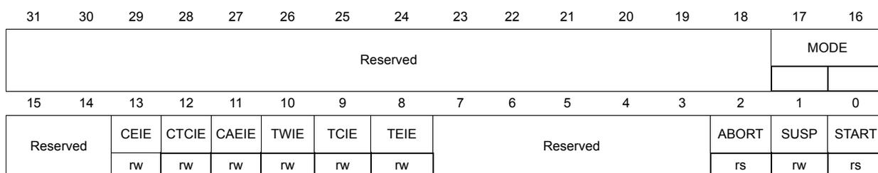
| 31 | 30 | 29 | 28 | 27 | 26 | 25 | 24 | 23 | 22 | 21 | 20 | 19 | 18 | 17 | 16 | |
| Reserved | MODE | |||||||||||||||
| 15 | 14 | 13 | 12 | 11 | 10 | 9 | 8 | 7 | 6 | 5 | 4 | 3 | 2 | 1 | 0 | |
| Reserved | CEIE | CTCIE | CAEIE | TWIE | TCIE | TEIE | Reserved | ABORT | SUSP | START | ||||||
| rw | rw | rw | rw | rw | rw | rs | rw | rs | ||||||||
Bits 31:18 Reserved, must be kept at reset value
Bits 17:16 MODE : DMA2D mode
This bit is set and cleared by software. It cannot be modified while a transfer is ongoing.
00: Memory-to-memory (FG fetch only)
01: Memory-to-memory with PFC (FG fetch only with FG PFC active)
10: Memory-to-memory with blending (FG and BG fetch with PFC and blending)
11: Register-to-memory (no FG nor BG, only output stage active)
Bits 15:14 Reserved, must be kept at reset value
Bit 13 CEIE : Configuration Error Interrupt Enable
This bit is set and cleared by software.
0: CE interrupt disable
1: CE interrupt enable
Bit 12 CTCIE : CLUT transfer complete interrupt enable
This bit is set and cleared by software.
0: CTC interrupt disable
1: CTC interrupt enable
Bit 11 CAEIE : CLUT access error interrupt enable
This bit is set and cleared by software.
0: CAE interrupt disable
1: CAE interrupt enable
Bit 10 TWIE : Transfer watermark interrupt enable
This bit is set and cleared by software.
0: TW interrupt disable
1: TW interrupt enable
Bit 9 TCIE : Transfer complete interrupt enable
This bit is set and cleared by software.
0: TC interrupt disable
1: TC interrupt enable
Bit 8 TEIE : Transfer error interrupt enable
This bit is set and cleared by software.
0: TE interrupt disable
1: TE interrupt enable
Bits 7:3 Reserved, must be kept at reset value
Bit 2 ABORT : Abort
This bit can be used to abort the current transfer. This bit is set by software and is automatically reset by hardware when the START bit is reset.
0: No transfer abort requested
1: Transfer abort requested
Bit 1 SUSP : Suspend
This bit can be used to suspend the current transfer. This bit is set and reset by software. It is automatically reset by hardware when the START bit is reset.
0: Transfer not suspended
1: Transfer suspended
Bit 0 START : Start
This bit can be used to launch the DMA2D according to the parameters loaded in the various configuration registers. This bit is automatically reset by the following events:
- – At the end of the transfer
- – When the data transfer is aborted by the user application by setting the ABORT bit in DMA2D_CR
- – When a data transfer error occurs
- – When the data transfer has not started due to a configuration error or another transfer operation already ongoing (automatic CLUT loading).
11.5.2 DMA2D Interrupt Status Register (DMA2D_ISR)
Address offset: 0x0004
Reset value: 0x0000 0000
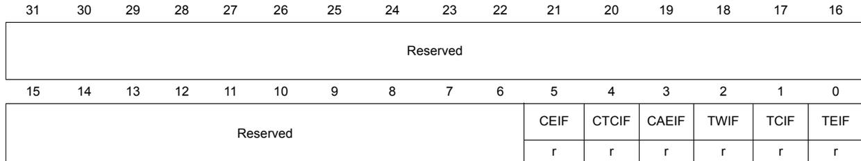
| 31 | 30 | 29 | 28 | 27 | 26 | 25 | 24 | 23 | 22 | 21 | 20 | 19 | 18 | 17 | 16 |
| Reserved | |||||||||||||||
| 15 | 14 | 13 | 12 | 11 | 10 | 9 | 8 | 7 | 6 | 5 | 4 | 3 | 2 | 1 | 0 |
| Reserved | CEIF | CTCIF | CAEIF | TWIF | TCIF | TEIF | |||||||||
| r | r | r | r | r | r | ||||||||||
Bits 31:6 Reserved, must be kept at reset value
Bit 5 CEIF : Configuration error interrupt flag
This bit is set when the START bit of DMA2D_CR, DMA2DFGPFCCR or DMA2D_BGPFCCR is set and a wrong configuration has been programmed.
Bit 4 CTCIF : CLUT transfer complete interrupt flag
This bit is set when the CLUT copy from a system memory area to the internal DMA2D memory is complete.
Bit 3 CAEIF : CLUT access error interrupt flag
This bit is set when the CPU accesses the CLUT while the CLUT is being automatically copied from a system memory to the internal DMA2D.
Bit 2 TWIF : Transfer watermark interrupt flag
This bit is set when the last pixel of the watermarked line has been transferred.
Bit 1 TCIF : Transfer complete interrupt flag
This bit is set when a DMA2D transfer operation is complete (data transfer only).
Bit 0 TEIF : Transfer error interrupt flag
This bit is set when an error occurs during a DMA transfer (data transfer or automatic CLUT loading).
11.5.3 DMA2D interrupt flag clear register (DMA2D_IFCR)
Address offset: 0x0008
Reset value: 0x0000 0000
| 31 | 30 | 29 | 28 | 27 | 26 | 25 | 24 | 23 | 22 | 21 | 20 | 19 | 18 | 17 | 16 |
| Reserved | |||||||||||||||
| 15 | 14 | 13 | 12 | 11 | 10 | 9 | 8 | 7 | 6 | 5 | 4 | 3 | 2 | 1 | 0 |
| Reserved | CCEIF | CCTCIF | CAECIF | CTWIF | CTCIF | CTEIF | |||||||||
| rc_w1 | rc_w1 | rc_w1 | rc_w1 | rc_w1 | rc_w1 | ||||||||||
Bits 31:6 Reserved, must be kept at reset value
Bit 5 CCEIF : Clear configuration error interrupt flag
Programming this bit to 1 clears the CEIF flag in the DMA2D_ISR register
Bit 4 CCTCIF : Clear CLUT transfer complete interrupt flag
Programming this bit to 1 clears the CTCIF flag in the DMA2D_ISR register
Bit 3 CAECIF : Clear CLUT access error interrupt flag
Programming this bit to 1 clears the CAEIF flag in the DMA2D_ISR register
Bit 2 CTWIF : Clear transfer watermark interrupt flag
Programming this bit to 1 clears the TWIF flag in the DMA2D_ISR register
Bit 1 CTCIF : Clear transfer complete interrupt flag
Programming this bit to 1 clears the TCIF flag in the DMA2D_ISR register
Bit 0 CTEIF : Clear Transfer error interrupt flag
Programming this bit to 1 clears the TEIF flag in the DMA2D_ISR register
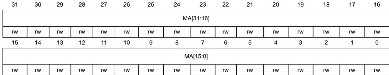
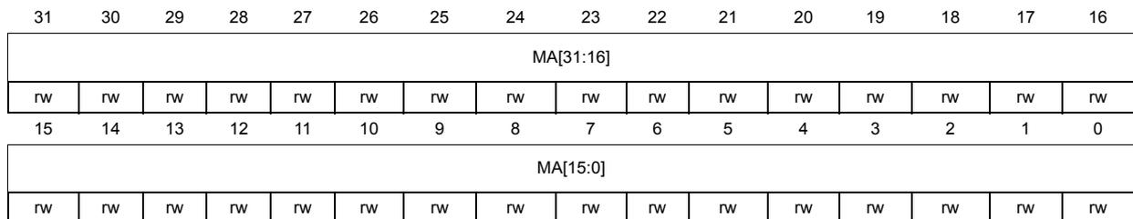
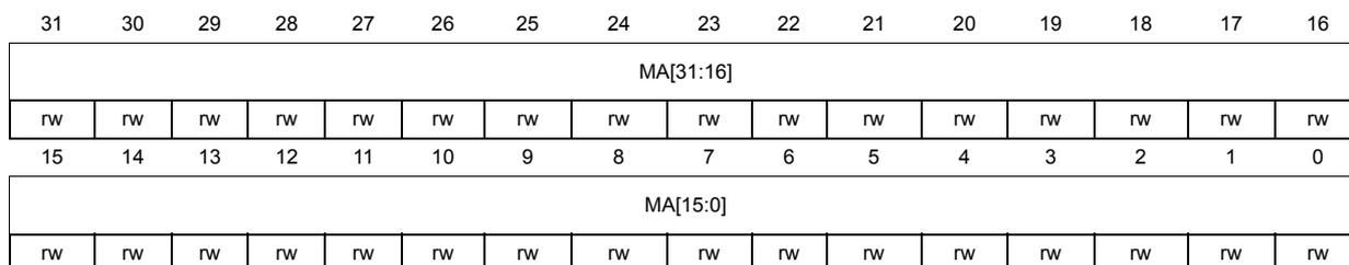
11.5.4 DMA2D foreground memory address register (DMA2D_FGMAR)
Address offset: 0x000C
Reset value: 0x0000 0000
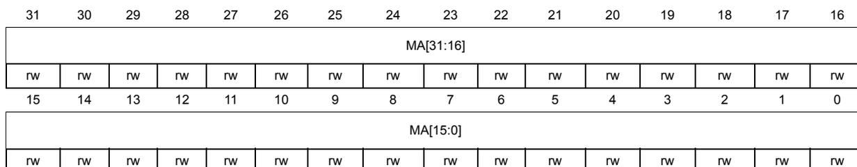
| 31 | 30 | 29 | 28 | 27 | 26 | 25 | 24 | 23 | 22 | 21 | 20 | 19 | 18 | 17 | 16 |
| MA[31:16] | |||||||||||||||
| rw | rw | rw | rw | rw | rw | rw | rw | rw | rw | rw | rw | rw | rw | rw | rw |
| 15 | 14 | 13 | 12 | 11 | 10 | 9 | 8 | 7 | 6 | 5 | 4 | 3 | 2 | 1 | 0 |
| MA[15:0] | |||||||||||||||
| rw | rw | rw | rw | rw | rw | rw | rw | rw | rw | rw | rw | rw | rw | rw | rw |
Bits 31:0 MA[31: 0] : Memory address
Address of the data used for the foreground image. This register can only be written when data transfers are disabled. Once the data transfer has started, this register is read-only.
The address alignment must match the image format selected e.g. a 32-bit per pixel format must be 32-bit aligned, a 16-bit per pixel format must be 16-bit aligned and a 4-bit per pixel format must be 8-bit aligned.
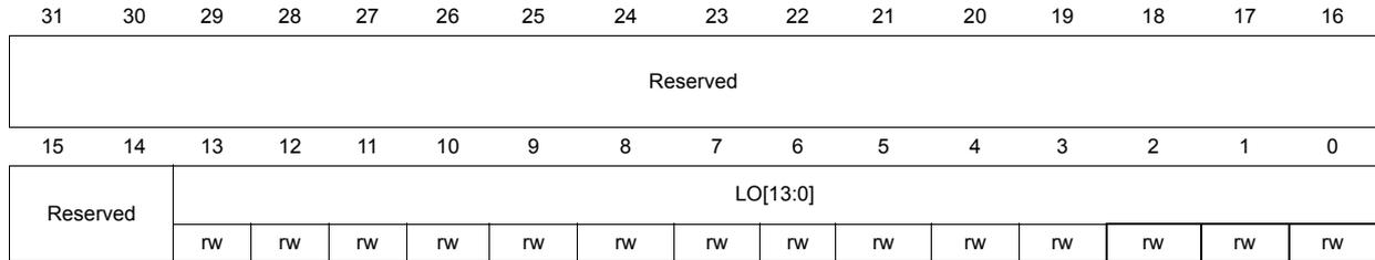
11.5.5 DMA2D foreground offset register (DMA2D_FGOR)
Address offset: 0x0010
Reset value: 0x0000 0000
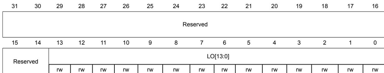
| 31 | 30 | 29 | 28 | 27 | 26 | 25 | 24 | 23 | 22 | 21 | 20 | 19 | 18 | 17 | 16 |
| Reserved | |||||||||||||||
| 15 | 14 | 13 | 12 | 11 | 10 | 9 | 8 | 7 | 6 | 5 | 4 | 3 | 2 | 1 | 0 |
| Reserved | LO[13:0] | ||||||||||||||
| rw | rw | rw | rw | rw | rw | rw | rw | rw | rw | rw | rw | rw | rw | ||
Bits 31:14 Reserved, must be kept at reset value
Bits 13:0 LO[13: 0] : Line offset
Line offset used for the foreground expressed in pixel. This value is used to generate the address. It is added at the end of each line to determine the starting address of the next line.
These bits can only be written when data transfers are disabled. Once a data transfer has started, they become read-only.
If the image format is 4-bit per pixel, the line offset must be even.
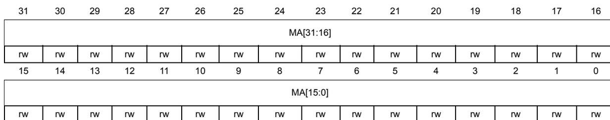
11.5.6 DMA2D background memory address register (DMA2D_BGMAR)
Address offset: 0x0014
Reset value: 0x0000 0000
| 31 | 30 | 29 | 28 | 27 | 26 | 25 | 24 | 23 | 22 | 21 | 20 | 19 | 18 | 17 | 16 |
| MA[31:16] | |||||||||||||||
| rw | rw | rw | rw | rw | rw | rw | rw | rw | rw | rw | rw | rw | rw | rw | rw |
| 15 | 14 | 13 | 12 | 11 | 10 | 9 | 8 | 7 | 6 | 5 | 4 | 3 | 2 | 1 | 0 |
| MA[15:0] | |||||||||||||||
| rw | rw | rw | rw | rw | rw | rw | rw | rw | rw | rw | rw | rw | rw | rw | rw |
Bits 31: 0 MA[31: 0] : Memory address
Address of the data used for the background image. This register can only be written when data transfers are disabled. Once a data transfer has started, this register is read-only.
The address alignment must match the image format selected e.g. a 32-bit per pixel format must be 32-bit aligned, a 16-bit per pixel format must be 16-bit aligned and a 4-bit per pixel format must be 8-bit aligned.
11.5.7 DMA2D background offset register (DMA2D_BGOR)
Address offset: 0x0018
Reset value: 0x0000 0000
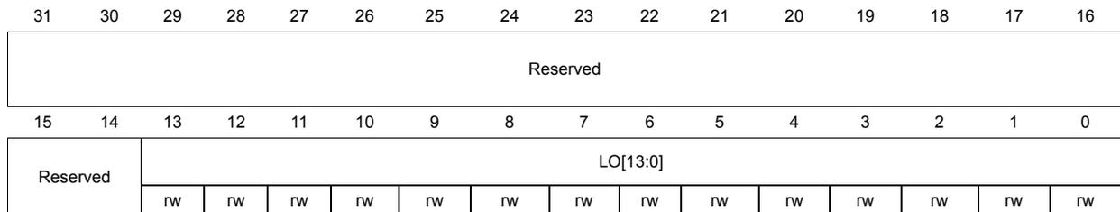
| 31 | 30 | 29 | 28 | 27 | 26 | 25 | 24 | 23 | 22 | 21 | 20 | 19 | 18 | 17 | 16 |
| Reserved | |||||||||||||||
| 15 | 14 | 13 | 12 | 11 | 10 | 9 | 8 | 7 | 6 | 5 | 4 | 3 | 2 | 1 | 0 |
| Reserved | LO[13:0] | ||||||||||||||
| rw | rw | rw | rw | rw | rw | rw | rw | rw | rw | rw | rw | rw | rw | ||
Bits 31:14 Reserved, must be kept at reset value
Bits 13:0 LO[13: 0] : Line offset
Line offset used for the background image (expressed in pixel). This value is used for the address generation. It is added at the end of each line to determine the starting address of the next line.
These bits can only be written when data transfers are disabled. Once data transfer has started, they become read-only.
If the image format is 4-bit per pixel, the line offset must be even.
11.5.8 DMA2D foreground PFC control register (DMA2D_FGPFCCR)
Address offset: 0x001C
Reset value: 0x0000 0000
| 31 | 30 | 29 | 28 | 27 | 26 | 25 | 24 | 23 | 22 | 21 | 20 | 19 | 18 | 17 | 16 |
|---|---|---|---|---|---|---|---|---|---|---|---|---|---|---|---|
| ALPHA[7:0] | Reserved | AM[1:0] | |||||||||||||
| rw | rw | rw | rw | rw | rw | rw | rw | rw | rw | ||||||
| 15 | 14 | 13 | 12 | 11 | 10 | 9 | 8 | 7 | 6 | 5 | 4 | 3 | 2 | 1 | 0 |
| CS[7:0] | Reserved | START | CCM | CM[3:0] | |||||||||||
| rw | rw | rw | rw | rw | rw | rw | rw | rs | rw | rw | rw | rw | rw | ||
Bits 31:24 ALPHA[7: 0] : Alpha value
These bits define a fixed alpha channel value which can replace the original alpha value or be multiplied by the original alpha value according to the alpha mode selected through the AM[1:0] bits.
These bits can only be written when data transfers are disabled. Once a transfer has started, they become read-only.
Bits 23:18 Reserved, must be kept at reset value
Bits 17:16 AM[1: 0] : Alpha mode
These bits select the alpha channel value to be used for the foreground image. They can only be written data the transfer are disabled. Once the transfer has started, they become read-only.
00: No modification of the foreground image alpha channel value
01: Replace original foreground image alpha channel value by ALPHA[7: 0]
10: Replace original foreground image alpha channel value by ALPHA[7:0] multiplied with original alpha channel value
other configurations are meaningless
Bits 15:8 CS[7: 0] : CLUT size
These bits define the size of the CLUT used for the foreground image. Once the CLUT transfer has started, this field is read-only.
The number of CLUT entries is equal to CS[7:0] + 1.
Bits 7:6 Reserved, must be kept at reset value
Bit 5 START : StartThis bit can be set to start the automatic loading of the CLUT. It is automatically reset:
- – at the end of the transfer
- – when the transfer is aborted by the user application by setting the ABORT bit in DMA2D_CR
- – when a transfer error occurs
- – when the transfer has not started due to a configuration error or another transfer operation already ongoing (data transfer or automatic background CLUT transfer).
This bit defines the color format of the CLUT. It can only be written when the transfer is disabled. Once the CLUT transfer has started, this bit is read-only.
0: ARGB8888
1: RGB888
others: meaningless
Bits 3:0 CM[3: 0] : Color modeThese bits defines the color format of the foreground image. They can only be written when data transfers are disabled. Once the transfer has started, they are read-only.
0000: ARGB8888
0001: RGB888
0010: RGB565
0011: ARGB1555
0100: ARGB4444
0101: L8
0110: AL44
0111: AL88
1000: L4
1001: A8
1010: A4
others: meaningless
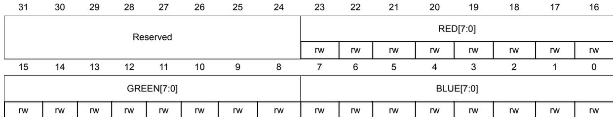
11.5.9 DMA2D foreground color register (DMA2D_FGCOLR)
Address offset: 0x0020
Reset value: 0x0000 0000
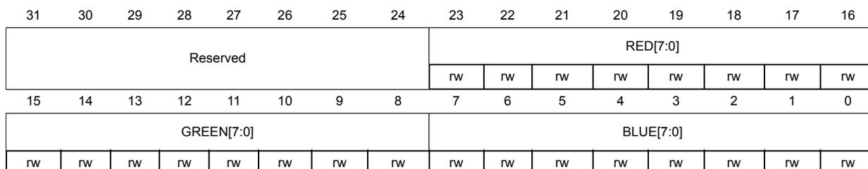
| 31 | 30 | 29 | 28 | 27 | 26 | 25 | 24 | 23 | 22 | 21 | 20 | 19 | 18 | 17 | 16 |
| Reserved | RED[7:0] | ||||||||||||||
| rw | rw | rw | rw | rw | rw | rw | rw | ||||||||
| 15 | 14 | 13 | 12 | 11 | 10 | 9 | 8 | 7 | 6 | 5 | 4 | 3 | 2 | 1 | 0 |
| GREEN[7:0] | BLUE[7:0] | ||||||||||||||
| rw | rw | rw | rw | rw | rw | rw | rw | rw | rw | rw | rw | rw | rw | rw | rw |
Bits 31:24 Reserved, must be kept at reset value
Bits 23:16 RED[7: 0] : Red Value
These bits defines the red value for the A4 or A8 mode of the foreground image. They can only be written when data transfers are disabled. Once the transfer has started, they are read-only.
Bits 15:8 GREEN[7: 0] : Green Value
These bits defines the green value for the A4 or A8 mode of the foreground image. They can only be written when data transfers are disabled. Once the transfer has started, They are read-only.
Bits 7:0 BLUE[7: 0] : Blue Value
These bits defines the blue value for the A4 or A8 mode of the foreground image. They can only be written when data transfers are disabled. Once the transfer has started, They are read-only.
11.5.10 DMA2D background PFC control register (DMA2D_BGPFCR)
Address offset: 0x0024
Reset value: 0x0000 0000
| 31 | 30 | 29 | 28 | 27 | 26 | 25 | 24 | 23 | 22 | 21 | 20 | 19 | 18 | 17 | 16 |
|---|---|---|---|---|---|---|---|---|---|---|---|---|---|---|---|
| ALPHA[7:0] | Reserved | AM[1:0] | |||||||||||||
| rw | rw | rw | rw | rw | rw | rw | rw | rw | rw | ||||||
| 15 | 14 | 13 | 12 | 11 | 10 | 9 | 8 | 7 | 6 | 5 | 4 | 3 | 2 | 1 | 0 |
| CS[7:0] | Reserved | START | CCM | CM[3:0] | |||||||||||
| rw | rw | rw | rw | rw | rw | rw | rw | rs | rw | rw | rw | rw | rw | ||
Bits 31:24 ALPHA[7: 0] : Alpha value
These bits define a fixed alpha channel value which can replace the original alpha value or be multiplied with the original alpha value according to the alpha mode selected with bits AM[1: 0]. These bits can only be written when data transfers are disabled. Once the transfer has started, they are read-only.
Bits 23:18 Reserved, must be kept at reset value
Bits 17:16 AM[1: 0] : Alpha mode
These bits define which alpha channel value to be used for the background image. These bits can only be written when data transfers are disabled. Once the transfer has started, they are read-only.
00: No modification of the foreground image alpha channel value
01: Replace original background image alpha channel value by ALPHA[7: 0]
10: Replace original background image alpha channel value by ALPHA[7:0] multiplied with original alpha channel value
others: meaningless
Bits 15:8 CS[7: 0] : CLUT size
These bits define the size of the CLUT used for the BG. Once the CLUT transfer has started, this field is read-only.
The number of CLUT entries is equal to CS[7:0] + 1.
Bits 7:6 Reserved, must be kept at reset value
Bit 5 START: StartThis bit is set to start the automatic loading of the CLUT. This bit is automatically reset:
- – at the end of the transfer
- – when the transfer is aborted by the user application by setting the ABORT bit in the DMA2D_CR
- – when a transfer error occurs
- – when the transfer has not started due to a configuration error or another transfer operation already on going (data transfer or automatic foreground CLUT transfer).
These bits define the color format of the CLUT. This register can only be written when the transfer is disabled. Once the CLUT transfer has started, this bit is read-only.
0: ARGB8888
1: RGB888
others: meaningless
Bits 3:0 CM[3: 0]: Color modeThese bits define the color format of the foreground image. These bits can only be written when data transfers are disabled. Once the transfer has started, they are read-only.
0000: ARGB8888
0001: RGB888
0010: RGB565
0011: ARGB1555
0100: ARGB4444
0101: L8
0110: AL44
0111: AL88
1000: L4
1001: A8
1010: A4
others: meaningless
11.5.11 DMA2D background color register (DMA2D_BGCOLR)
Address offset: 0x0028
Reset value: 0x0000 0000
| 31 | 30 | 29 | 28 | 27 | 26 | 25 | 24 | 23 | 22 | 21 | 20 | 19 | 18 | 17 | 16 |
| Reserved | RED[7:0] | ||||||||||||||
| rw | rw | rw | rw | rw | rw | rw | rw | ||||||||
| 15 | 14 | 13 | 12 | 11 | 10 | 9 | 8 | 7 | 6 | 5 | 4 | 3 | 2 | 1 | 0 |
| GREEN[7:0] | BLUE[7:0] | ||||||||||||||
| rw | rw | rw | rw | rw | rw | rw | rw | rw | rw | rw | rw | rw | rw | rw | rw |
Bits 31:24 Reserved, must be kept at reset value
Bits 23:16 RED[7: 0] : Red Value
These bits define the red value for the A4 or A8 mode of the background. These bits can only be written when data transfers are disabled. Once the transfer has started, they are read-only.
Bits 15:8 GREEN[7: 0] : Green Value
These bits define the green value for the A4 or A8 mode of the background. These bits can only be written when data transfers are disabled. Once the transfer has started, they are read-only.
Bits 7:0 BLUE[7: 0] : Blue Value
These bits define the blue value for the A4 or A8 mode of the background. These bits can only be written when data transfers are disabled. Once the transfer has started, they are read-only.
11.5.12 DMA2D foreground CLUT memory address register (DMA2D_FGCMAR)
Address offset: 0x002C
Reset value: 0x0000 0000
| 31 | 30 | 29 | 28 | 27 | 26 | 25 | 24 | 23 | 22 | 21 | 20 | 19 | 18 | 17 | 16 |
| MA[31:16] | |||||||||||||||
| rw | rw | rw | rw | rw | rw | rw | rw | rw | rw | rw | rw | rw | rw | rw | rw |
| 15 | 14 | 13 | 12 | 11 | 10 | 9 | 8 | 7 | 6 | 5 | 4 | 3 | 2 | 1 | 0 |
| MA[15:0] | |||||||||||||||
| rw | rw | rw | rw | rw | rw | rw | rw | rw | rw | rw | rw | rw | rw | rw | rw |
Bits 31: 0 MA[31: 0] : Memory Address
Address of the data used for the CLUT address dedicated to the foreground image. This register can only be written when no transfer is ongoing. Once the CLUT transfer has started, this register is read-only.
If the foreground CLUT format is 32-bit, the address must be 32-bit aligned.
11.5.13 DMA2D background CLUT memory address register (DMA2D_BGCMAR)
Address offset: 0x0030
Reset value: 0x0000 0000
| 31 | 30 | 29 | 28 | 27 | 26 | 25 | 24 | 23 | 22 | 21 | 20 | 19 | 18 | 17 | 16 |
| MA[31:16] | |||||||||||||||
| rw | rw | rw | rw | rw | rw | rw | rw | rw | rw | rw | rw | rw | rw | rw | rw |
| 15 | 14 | 13 | 12 | 11 | 10 | 9 | 8 | 7 | 6 | 5 | 4 | 3 | 2 | 1 | 0 |
| MA[15:0] | |||||||||||||||
| rw | rw | rw | rw | rw | rw | rw | rw | rw | rw | rw | rw | rw | rw | rw | rw |
Bits 31: 0 MA[31: 0] : Memory address
Address of the data used for the CLUT address dedicated to the background image.
This register can only be written when no transfer is on going. Once the CLUT transfer has started, this register is read-only.
If the background CLUT format is 32-bit, the address must be 32-bit aligned.
11.5.14 DMA2D output PFC control register (DMA2D_OPFCCR)
Address offset: 0x0034
Reset value: 0x0000 0000
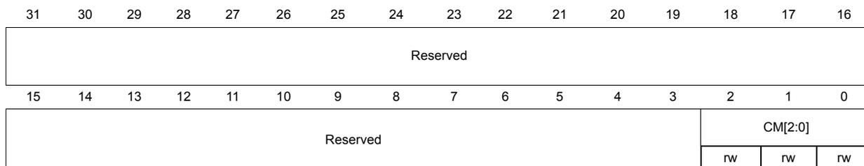
| 31 | 30 | 29 | 28 | 27 | 26 | 25 | 24 | 23 | 22 | 21 | 20 | 19 | 18 | 17 | 16 |
| Reserved | |||||||||||||||
| 15 | 14 | 13 | 12 | 11 | 10 | 9 | 8 | 7 | 6 | 5 | 4 | 3 | 2 | 1 | 0 |
| Reserved | CM[2:0] | ||||||||||||||
| rw | rw | rw | |||||||||||||
Bits 31: 3 Reserved, must be kept at reset value
Bits 2: 0 CM[2: 0] : Color mode
These bits define the color format of the output image. These bits can only be written when data transfers are disabled. Once the transfer has started, they are read-only.
000: ARGB8888
001: RGB888
010: RGB565
011: ARGB1555
100: ARGB4444
others: meaningless
11.5.15 DMA2D output color register (DMA2D_OCOLR)
Address offset: 0x0038
Reset value: 0x0000 0000
| 31 | 30 | 29 | 28 | 27 | 26 | 25 | 24 | 23 | 22 | 21 | 20 | 19 | 18 | 17 | 16 |
|---|---|---|---|---|---|---|---|---|---|---|---|---|---|---|---|
| ALPHA[7:0] | RED[7:0] | ||||||||||||||
| rw | rw | rw | rw | rw | rw | rw | rw | rw | rw | rw | rw | rw | rw | rw | rw |
| 15 | 14 | 13 | 12 | 11 | 10 | 9 | 8 | 7 | 6 | 5 | 4 | 3 | 2 | 1 | 0 |
| GREEN[7:0] | BLUE[7:0] | ||||||||||||||
| RED[4:0] | GREEN[5:0] | BLUE[4:0] | |||||||||||||
| A | RED[4:0] | GREEN[4:0] | BLUE[4:0] | ||||||||||||
| ALPHA[3:0] | RED[3:0] | GREEN[3:0] | BLUE[3:0] | ||||||||||||
| rw | rw | rw | rw | rw | rw | rw | rw | rw | rw | rw | rw | rw | rw | rw | rw |
Bits 31:24 ALPHA[7: 0] : Alpha Channel Value
These bits define the alpha channel of the output color. These bits can only be written when data transfers are disabled. Once the transfer has started, they are read-only.
Bits 23:16 RED[7: 0] : Red Value
These bits define the red value of the output image. These bits can only be written when data transfers are disabled. Once the transfer has started, they are read-only.
Bits 15:8 GREEN[7: 0] : Green Value
These bits define the green value of the output image. These bits can only be written when data transfers are disabled. Once the transfer has started, they are read-only.
Bits 7:0 BLUE[7: 0] : Blue Value
These bits define the blue value of the output image. These bits can only be written when data transfers are disabled. Once the transfer has started, they are read-only.
11.5.16 DMA2D output memory address register (DMA2D_OMAR)Address offset: 0x003C
Reset value: 0x0000 0000
| 31 | 30 | 29 | 28 | 27 | 26 | 25 | 24 | 23 | 22 | 21 | 20 | 19 | 18 | 17 | 16 |
| MA[31:16] | |||||||||||||||
| rw | rw | rw | rw | rw | rw | rw | rw | rw | rw | rw | rw | rw | rw | rw | rw |
| 15 | 14 | 13 | 12 | 11 | 10 | 9 | 8 | 7 | 6 | 5 | 4 | 3 | 2 | 1 | 0 |
| MA[15:0] | |||||||||||||||
| rw | rw | rw | rw | rw | rw | rw | rw | rw | rw | rw | rw | rw | rw | rw | rw |
Address of the data used for the output FIFO. These bits can only be written when data transfers are disabled. Once the transfer has started, they are read-only.
The address alignment must match the image format selected e.g. a 32-bit per pixel format must be 32-bit aligned and a 16-bit per pixel format must be 16-bit aligned.
11.5.17 DMA2D output offset register (DMA2D_OOR)
Address offset: 0x0040
Reset value: 0x0000 0000
| 31 | 30 | 29 | 28 | 27 | 26 | 25 | 24 | 23 | 22 | 21 | 20 | 19 | 18 | 17 | 16 |
| Reserved | |||||||||||||||
| 15 | 14 | 13 | 12 | 11 | 10 | 9 | 8 | 7 | 6 | 5 | 4 | 3 | 2 | 1 | 0 |
| Reserved | LO[13:0] | ||||||||||||||
| rw | rw | rw | rw | rw | rw | rw | rw | rw | rw | rw | rw | rw | rw | rw | rw |
Bits 31:14 Reserved, must be kept at reset value
Bits 13:0 LO[13: 0] : Line Offset
Line offset used for the output (expressed in pixels). This value is used for the address generation. It is added at the end of each line to determine the starting address of the next line. These bits can only be written when data transfers are disabled. Once the transfer has started, they are read-only.
11.5.18 DMA2D number of line register (DMA2D_NLR)
Address offset: 0x0044
Reset value: 0x0000 0000
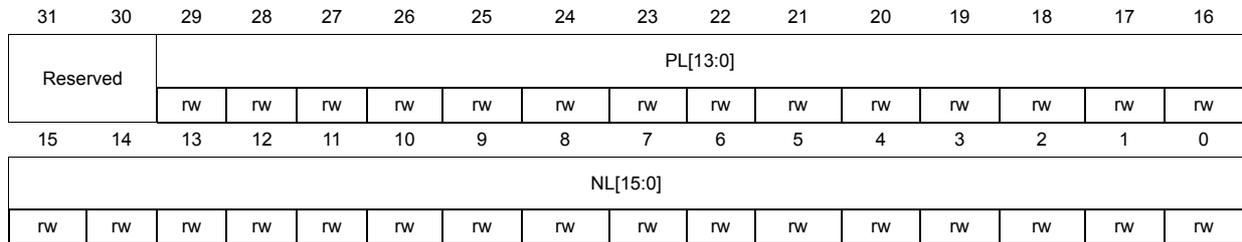
| 31 | 30 | 29 | 28 | 27 | 26 | 25 | 24 | 23 | 22 | 21 | 20 | 19 | 18 | 17 | 16 |
| Reserved | PL[13:0] | ||||||||||||||
| rw | rw | rw | rw | rw | rw | rw | rw | rw | rw | rw | rw | rw | rw | rw | rw |
| 15 | 14 | 13 | 12 | 11 | 10 | 9 | 8 | 7 | 6 | 5 | 4 | 3 | 2 | 1 | 0 |
| NL[15:0] | |||||||||||||||
| rw | rw | rw | rw | rw | rw | rw | rw | rw | rw | rw | rw | rw | rw | rw | rw |
Bits 31:30 Reserved, must be kept at reset value
Bits 29:16 PL[13: 0] : Pixel per lines
Number of pixels per lines of the area to be transferred. These bits can only be written when data transfers are disabled. Once the transfer has started, they are read-only. If any of the input image format is 4-bit per pixel, pixel per lines must be even.
Bits 15:0 NL[15: 0] : Number of lines
Number of lines of the area to be transferred. These bits can only be written when data transfers are disabled. Once the transfer has started, they are read-only.
11.5.19 DMA2D line watermark register (DMA2D_LWR)
Address offset: 0x0048
Reset value: 0x0000 0000
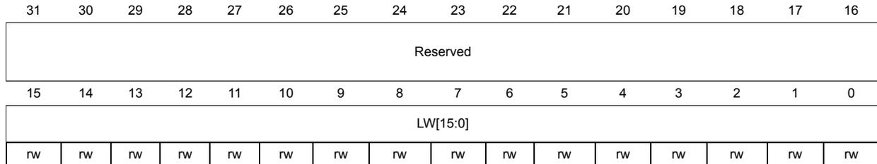
| 31 | 30 | 29 | 28 | 27 | 26 | 25 | 24 | 23 | 22 | 21 | 20 | 19 | 18 | 17 | 16 |
| Reserved | |||||||||||||||
| 15 | 14 | 13 | 12 | 11 | 10 | 9 | 8 | 7 | 6 | 5 | 4 | 3 | 2 | 1 | 0 |
| LW[15:0] | |||||||||||||||
| rw | rw | rw | rw | rw | rw | rw | rw | rw | rw | rw | rw | rw | rw | rw | rw |
Bits 31:16 Reserved, must be kept at reset value
Bits 15:0 LW[15:0] : Line watermark
- These bits allow to configure the line watermark for interrupt generation.
- An interrupt is raised when the last pixel of the watermarked line has been transferred.
- These bits can only be written when data transfers are disabled. Once the transfer has started, they are read-only.
11.5.20 DMA2D AHB master timer configuration register (DMA2D_AMTCR)
Address offset: 0x004C
Reset value: 0x0000 0000
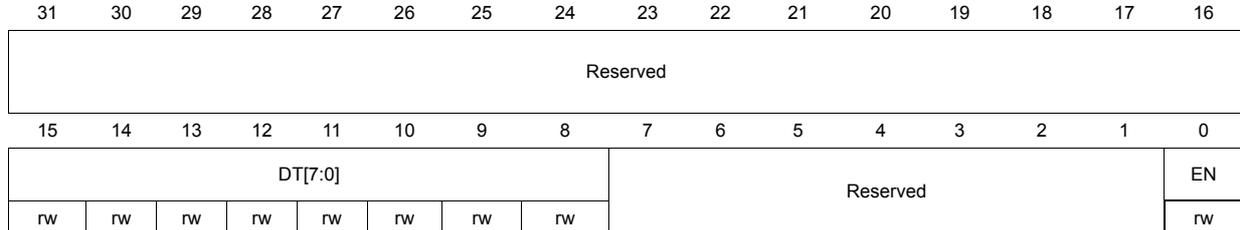
| 31 | 30 | 29 | 28 | 27 | 26 | 25 | 24 | 23 | 22 | 21 | 20 | 19 | 18 | 17 | 16 |
| Reserved | |||||||||||||||
| 15 | 14 | 13 | 12 | 11 | 10 | 9 | 8 | 7 | 6 | 5 | 4 | 3 | 2 | 1 | 0 |
| DT[7:0] | Reserved | EN | |||||||||||||
| rw | rw | rw | rw | rw | rw | rw | rw | rw | |||||||
Bits 31:16 Reserved
Bits 15:8 DT[7:0] : Dead Time
Dead time value in the AHB clock cycle inserted between two consecutive accesses on the AHB master port. These bits represent the minimum guaranteed number of cycles between two consecutive AHB accesses.
Bits 7:1 Reserved
Bit 0 EN : Enable
Enables the dead time functionality.
11.5.21 DMA2D register map
The following table summarizes the DMA2D registers. Refer to Section 2.3: Memory map for the DMA2D register base address.
Table 61. DMA2D register map and reset values
| Offset | Register | 31 | 30 | 29 | 28 | 27 | 26 | 25 | 24 | 23 | 22 | 21 | 20 | 19 | 18 | 17 | 16 | 15 | 14 | 13 | 12 | 11 | 10 | 9 | 8 | 7 | 6 | 5 | 4 | 3 | 2 | 1 | 0 |
|---|---|---|---|---|---|---|---|---|---|---|---|---|---|---|---|---|---|---|---|---|---|---|---|---|---|---|---|---|---|---|---|---|---|
| 0x0000 | DMA2D_CR | Reserved | MODE[1:0] | Reserved | CEIE | CTOIE | CAEIE | TWIE | TCIE | TEIE | Reserved | ABORT | SUSP | START | |||||||||||||||||||
| Reset value | 0 | 0 | 0 | 0 | 0 | 0 | 0 | 0 | 0 | 0 | |||||||||||||||||||||||
| 0x0004 | DMA2D_ISR | Reserved | CEIF | CTCIF | CAEIF | TWIF | TCIF | TEIF | |||||||||||||||||||||||||
| Reset value | 0 | 0 | 0 | 0 | 0 | 0 | |||||||||||||||||||||||||||
| 0x0008 | DMA2D_IFCR | Reserved | CCEIF | CCTCIF | CAECIF | CTWIF | CTCIF | CTEIF | |||||||||||||||||||||||||
| Reset value | 0 | 0 | 0 | 0 | 0 | 0 | |||||||||||||||||||||||||||
| 0x000C | DMA2D_FGMAR | MA[31:0] | |||||||||||||||||||||||||||||||
| Reset value | 0 | ||||||||||||||||||||||||||||||||
| 0x0010 | DMA2D_FGOR | Reserved | LO[13:0] | ||||||||||||||||||||||||||||||
| Reset value | 0 | ||||||||||||||||||||||||||||||||
| 0x0014 | DMA2D_BGMAR | MA[31:0] | |||||||||||||||||||||||||||||||
| Reset value | 0 | ||||||||||||||||||||||||||||||||
| 0x0018 | DMA2D_BGOR | Reserved | LO[13:0] | ||||||||||||||||||||||||||||||
| Reset value | 0 | ||||||||||||||||||||||||||||||||
| 0x001C | DMA2D_FGPFCCR | ALPHA[7:0] | Reserved | AM[1:0] | CS[7:0] | Res | START | CCM | CM[3:0] | ||||||||||||||||||||||||
| Reset value | 0 | 0 | 0 | 0 | 0 | ||||||||||||||||||||||||||||
| 0x0020 | DMA2D_FGCOLR | ALPHA[7:0] | RED[7:0] | GREEN[7:0] | BLUE[7:0] | ||||||||||||||||||||||||||||
| Reset value | 0 | ||||||||||||||||||||||||||||||||
| 0x0024 | DMA2D_BGPFCCR | ALPHA[7:0] | Reserved | AM[1:0] | CS[7:0] | Res | START | CCM | CM[3:0] | ||||||||||||||||||||||||
| Reset value | 0 | 0 | 0 | 0 | 0 | ||||||||||||||||||||||||||||
| 0x0028 | DMA2D_BGCOLR | ALPHA[7:0] | RED[7:0] | GREEN[7:0] | BLUE[7:0] | ||||||||||||||||||||||||||||
| Reset value | 0 | ||||||||||||||||||||||||||||||||
| 0x002C | DMA2D_FGCMAR | MA[31:0] | |||||||||||||||||||||||||||||||
| Reset value | 0 | ||||||||||||||||||||||||||||||||
| 0x0030 | DMA2D_BGCMAR | MA[31:0] | |||||||||||||||||||||||||||||||
| Reset value | 0 | ||||||||||||||||||||||||||||||||
| 0x0034 | DMA2D_OPFCCR | Reserved | CM[2:0] | ||||||||||||||||||||||||||||||
| Reset value | 0 | ||||||||||||||||||||||||||||||||
| 0x0038 | DMA2D_OCOLR | ALPHA[7:0] | RED[7:0] | GREEN[7:0] | |||||||||||||||||||||||||||||
| Reserved | |||||||||||||||||||||||||||||||||
| Reserved | |||||||||||||||||||||||||||||||||
| Reserved | |||||||||||||||||||||||||||||||||
| Reserved | |||||||||||||||||||||||||||||||||
| 0x003C | DMA2D_OMAR | MA[31:0] | |||||||||||||||||||||||||||||||
| Reset value | 0 | ||||||||||||||||||||||||||||||||
Table 61. DMA2D register map and reset values (continued)
| Offset | Register | 31 | 30 | 29 | 28 | 27 | 26 | 25 | 24 | 23 | 22 | 21 | 20 | 19 | 18 | 17 | 16 | 15 | 14 | 13 | 12 | 11 | 10 | 9 | 8 | 7 | 6 | 5 | 4 | 3 | 2 | 1 | 0 |
|---|---|---|---|---|---|---|---|---|---|---|---|---|---|---|---|---|---|---|---|---|---|---|---|---|---|---|---|---|---|---|---|---|---|
| 0x0040 | DMA2D_OOR | Reserved | LO[13:0] | ||||||||||||||||||||||||||||||
| Reset value | 0 | 0 | 0 | 0 | 0 | 0 | 0 | 0 | 0 | 0 | 0 | 0 | 0 | 0 | |||||||||||||||||||
| 0x0044 | DMA2D_NLR | Res | PL[13:0] | NL[15:0] | |||||||||||||||||||||||||||||
| Reset value | 0 | 0 | 0 | 0 | 0 | 0 | 0 | 0 | 0 | 0 | 0 | 0 | 0 | 0 | 0 | 0 | 0 | 0 | 0 | 0 | 0 | 0 | 0 | 0 | 0 | 0 | 0 | 0 | 0 | 0 | 0 | ||
| 0x0048 | DMA2D_LWR | Reserved | LW[15:0] | ||||||||||||||||||||||||||||||
| Reset value | 0 | 0 | 0 | 0 | 0 | 0 | 0 | 0 | 0 | 0 | 0 | 0 | 0 | 0 | 0 | 0 | |||||||||||||||||
| 0x004C | DMA2D_AMTCR | Reserved | DT[7:0] | Reserved | EN | ||||||||||||||||||||||||||||
| Reset value | 0 | 0 | 0 | 0 | 0 | 0 | 0 | 0 | 0 | ||||||||||||||||||||||||
| 0x0050-0x03FF | - | Reserved | |||||||||||||||||||||||||||||||
| 0x0400-0x07FF | DMA2D_FGCLUT | APLHA[7:0][255:0] | RED[7:0][255:0] | GREEN[7:0][255:0] | BLUE[7:0][255:0] | ||||||||||||||||||||||||||||
| Reset value | X | X | X | X | X | X | X | X | X | X | X | X | X | X | X | X | X | X | X | X | X | X | X | X | X | X | X | X | X | X | X | X | |
| 0x0800-0x0BFF | DMA2D_BGCLUT | APLHA[7:0][255:0] | RED[7:0][255:0] | GREEN[7:0][255:0] | BLUE[7:0][255:0] | ||||||||||||||||||||||||||||
| Reset value | X | X | X | X | X | X | X | X | X | X | X | X | X | X | X | X | X | X | X | X | X | X | X | X | X | X | X | X | X | X | X | X | |