9. System configuration controller (SYSCFG)
The system configuration controller is mainly used to remap the memory accessible in the code area, select the Ethernet PHY interface and manage the external interrupt line connection to the GPIOs.
This section applies to the whole STM32F4xx family, unless otherwise specified.
9.1 I/O compensation cell
By default the I/O compensation cell is not used. However when the I/O output buffer speed is configured in 50 MHz or 100 MHz mode, it is recommended to use the compensation cell for slew rate control on I/O \( t_{f(I/O)out}/t_{r(I/O)out} \) commutation to reduce the I/O noise on power supply.
When the compensation cell is enabled, a READY flag is set to indicate that the compensation cell is ready and can be used. The I/O compensation cell can be used only when the supply voltage ranges from 2.4 to 3.6 V.
9.2 SYSCFG registers for STM32F405xx/07xx and STM32F415xx/17xx
9.2.1 SYSCFG memory remap register (SYSCFG_MEMRMP)
This register is used for specific configurations on memory remap:
- • Two bits are used to configure the type of memory accessible at address 0x0000 0000. These bits are used to select the physical remap by software and so, bypass the BOOT pins.
- • After reset these bits take the value selected by the BOOT pins. When booting from main Flash memory with BOOT pins set to 10 [(BOOT1,BOOT0) = (1,0)] this register takes the value 0x00.
When the FSMC is remapped at address 0x0000 0000, only the first two regions of Bank 1 memory controller (Bank1 NOR/PSRAM 1 and NOR/PSRAM 2) can be remapped. In remap mode, the CPU can access the external memory via ICode bus instead of System bus which boosts up the performance.
Address offset: 0x00
Reset value: 0x0000 000X (X is the memory mode selected by the BOOT pins)
| 31 | 30 | 29 | 28 | 27 | 26 | 25 | 24 | 23 | 22 | 21 | 20 | 19 | 18 | 17 | 16 |
|---|---|---|---|---|---|---|---|---|---|---|---|---|---|---|---|
| Reserved | |||||||||||||||
| 15 | 14 | 13 | 12 | 11 | 10 | 9 | 8 | 7 | 6 | 5 | 4 | 3 | 2 | 1 | 0 |
| Reserved | MEM_MODE | ||||||||||||||
| rw | rw | ||||||||||||||
Bits 31:2 Reserved, must be kept at reset value.
Bits 1:0 MEM_MODE : Memory mapping selection
Set and cleared by software. This bit controls the memory internal mapping at address 0x0000 0000. After reset these bits take the value selected by the Boot pins (except for FSMC).
- 00: Main Flash memory mapped at 0x0000 0000
- 01: System Flash memory mapped at 0x0000 0000
- 10: FSMC Bank1 (NOR/PSRAM 1 and 2) mapped at 0x0000 0000
- 11: Embedded SRAM (SRAM1) mapped at 0x0000 0000
Note: Refer to Section 2.3: Memory map for details about the memory mapping at address 0x0000 0000.
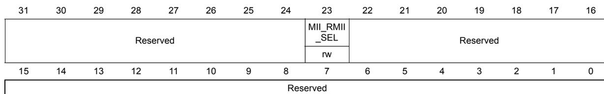
9.2.2 SYSCFG peripheral mode configuration register (SYSCFG_PMC)
Address offset: 0x04
Reset value: 0x0000 0000
| 31 | 30 | 29 | 28 | 27 | 26 | 25 | 24 | 23 | 22 | 21 | 20 | 19 | 18 | 17 | 16 |
|---|---|---|---|---|---|---|---|---|---|---|---|---|---|---|---|
| Reserved | MII_RMII _SEL | Reserved | |||||||||||||
| rw | |||||||||||||||
| 15 | 14 | 13 | 12 | 11 | 10 | 9 | 8 | 7 | 6 | 5 | 4 | 3 | 2 | 1 | 0 |
| Reserved | |||||||||||||||
Bits 31:24 Reserved, must be kept at reset value.
Bit 23 MII_RMII_SEL : Ethernet PHY interface selection
Set and Cleared by software. These bits control the PHY interface for the Ethernet MAC.
- 0: MII interface is selected
- 1: RMII PHY interface is selected
Note: This configuration must be done while the MAC is under reset and before enabling the MAC clocks.
Bits 22:0 Reserved, must be kept at reset value.
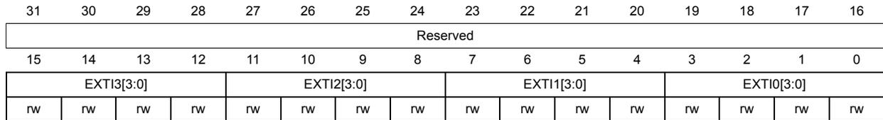
9.2.3 SYSCFG external interrupt configuration register 1 (SYSCFG_EXTICR1)
Address offset: 0x08
Reset value: 0x0000 0000
| 31 | 30 | 29 | 28 | 27 | 26 | 25 | 24 | 23 | 22 | 21 | 20 | 19 | 18 | 17 | 16 |
| Reserved | |||||||||||||||
| 15 | 14 | 13 | 12 | 11 | 10 | 9 | 8 | 7 | 6 | 5 | 4 | 3 | 2 | 1 | 0 |
| EXTI3[3:0] | EXTI2[3:0] | EXTI1[3:0] | EXTI0[3:0] | ||||||||||||
| rw | rw | rw | rw | rw | rw | rw | rw | rw | rw | rw | rw | rw | rw | rw | rw |
Bits 31:16 Reserved, must be kept at reset value.
Bits 15:0 EXTIx[3:0] : EXTI x configuration (x = 0 to 3)
These bits are written by software to select the source input for the EXTIx external interrupt.
0000: PA[x] pin
0001: PB[x] pin
0010: PC[x] pin
0011: PD[x] pin
0100: PE[x] pin
0101: PF[x] pin
0110: PG[x] pin
0111: PH[x] pin
1000: PI[x] pin
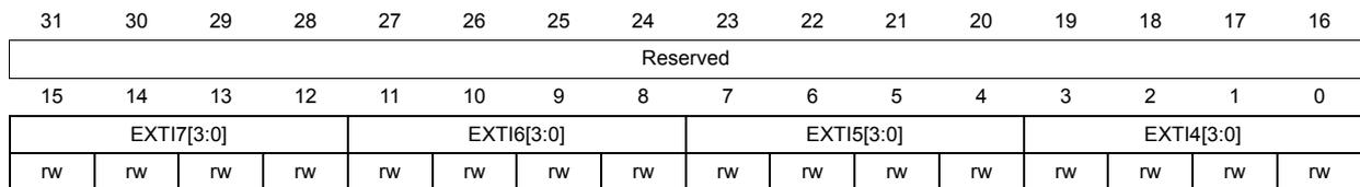
9.2.4 SYSCFG external interrupt configuration register 2 (SYSCFG_EXTICR2)
Address offset: 0x0C
Reset value: 0x0000 0000
| 31 | 30 | 29 | 28 | 27 | 26 | 25 | 24 | 23 | 22 | 21 | 20 | 19 | 18 | 17 | 16 |
| Reserved | |||||||||||||||
| 15 | 14 | 13 | 12 | 11 | 10 | 9 | 8 | 7 | 6 | 5 | 4 | 3 | 2 | 1 | 0 |
| EXTI7[3:0] | EXTI6[3:0] | EXTI5[3:0] | EXTI4[3:0] | ||||||||||||
| rw | rw | rw | rw | rw | rw | rw | rw | rw | rw | rw | rw | rw | rw | rw | rw |
Bits 31:16 Reserved, must be kept at reset value.
Bits 15:0 EXTIx[3:0] : EXTI x configuration (x = 4 to 7)
These bits are written by software to select the source input for the EXTIx external interrupt.
0000: PA[x] pin
0001: PB[x] pin
0010: PC[x] pin
0011: PD[x] pin
0100: PE[x] pin
0101: PF[x] pin
0110: PG[x] pin
0111: PH[x] pin
1000: PI[x] pin
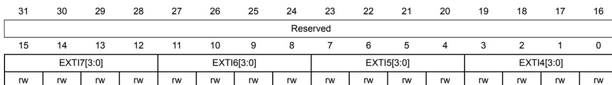
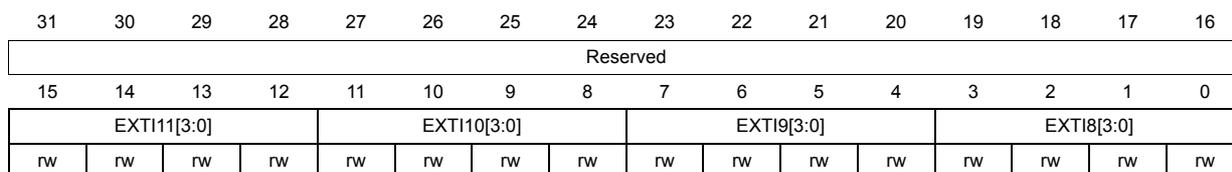
9.2.5 SYSCFG external interrupt configuration register 3 (SYSCFG_EXTICR3)
Address offset: 0x10
Reset value: 0x0000 0000
| 31 | 30 | 29 | 28 | 27 | 26 | 25 | 24 | 23 | 22 | 21 | 20 | 19 | 18 | 17 | 16 |
|---|---|---|---|---|---|---|---|---|---|---|---|---|---|---|---|
| Reserved | |||||||||||||||
| 15 | 14 | 13 | 12 | 11 | 10 | 9 | 8 | 7 | 6 | 5 | 4 | 3 | 2 | 1 | 0 |
| EXTI11[3:0] | EXTI10[3:0] | EXTI9[3:0] | EXTI8[3:0] | ||||||||||||
| rw | rw | rw | rw | rw | rw | rw | rw | rw | rw | rw | rw | rw | rw | rw | rw |
Bits 31:16 Reserved, must be kept at reset value.
Bits 15:0 EXTIx[3:0] : EXTI x configuration (x = 8 to 11)
These bits are written by software to select the source input for the EXTIx external interrupt.
0000: PA[x] pin
0001: PB[x] pin
0010: PC[x] pin
0011: PD[x] pin
0100: PE[x] pin
0101: PF[x] pin
0110: PG[x] pin
0111: PH[x] pin
1000: PI[x] pin
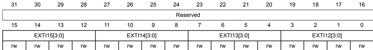
9.2.6 SYSCFG external interrupt configuration register 4 (SYSCFG_EXTICR4)
Address offset: 0x14
Reset value: 0x0000 0000
| 31 | 30 | 29 | 28 | 27 | 26 | 25 | 24 | 23 | 22 | 21 | 20 | 19 | 18 | 17 | 16 |
| Reserved | |||||||||||||||
| 15 | 14 | 13 | 12 | 11 | 10 | 9 | 8 | 7 | 6 | 5 | 4 | 3 | 2 | 1 | 0 |
| EXTI15[3:0] | EXTI14[3:0] | EXTI13[3:0] | EXTI12[3:0] | ||||||||||||
| rw | rw | rw | rw | rw | rw | rw | rw | rw | rw | rw | rw | rw | rw | rw | rw |
Bits 31:16 Reserved, must be kept at reset value.
Bits 15:0 EXTIx[3:0] : EXTI x configuration (x = 12 to 15)
These bits are written by software to select the source input for the EXTix external interrupt.
0000: PA[x] pin
0001: PB[x] pin
0010: PC[x] pin
0011: PD[x] pin
0100: PE[x] pin
0101: PF[x] pin
0110: PG[x] pin
0111: PH[x] pin
Note: PI[15:12] are not used.
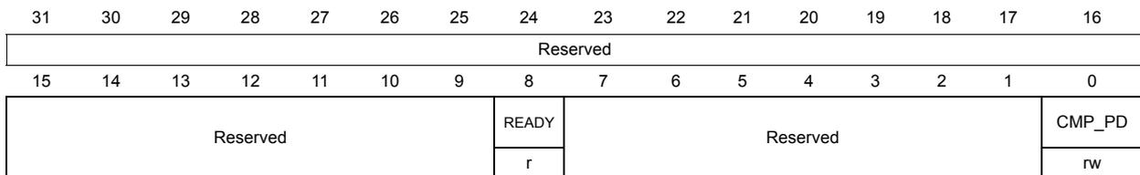
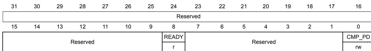
9.2.7 Compensation cell control register (SYSCFG_CMPCR)
Address offset: 0x20
Reset value: 0x0000 0000
| 31 | 30 | 29 | 28 | 27 | 26 | 25 | 24 | 23 | 22 | 21 | 20 | 19 | 18 | 17 | 16 |
| Reserved | |||||||||||||||
| 15 | 14 | 13 | 12 | 11 | 10 | 9 | 8 | 7 | 6 | 5 | 4 | 3 | 2 | 1 | 0 |
| Reserved | READY | Reserved | CMP_PD | ||||||||||||
| r | rw | ||||||||||||||
Bits 31:9 Reserved, must be kept at reset value.
Bit 8 READY : Compensation cell ready flag
0: I/O compensation cell not ready
1: I/O compensation cell ready
Bits 7:2 Reserved, must be kept at reset value.
Bit 0 CMP_PD : Compensation cell power-down
0: I/O compensation cell power-down mode
1: I/O compensation cell enabled
9.2.8 SYSCFG register maps for STM32F405xx/07xx and STM32F415xx/17xx
The following table gives the SYSCFG register map and the reset values.
Table 41. SYSCFG register map and reset values (STM32F405xx/07xx and STM32F415xx/17xx)
| Offset | Register | 31 | 30 | 29 | 28 | 27 | 26 | 25 | 24 | 23 | 22 | 21 | 20 | 19 | 18 | 17 | 16 | 15 | 14 | 13 | 12 | 11 | 10 | 9 | 8 | 7 | 6 | 5 | 4 | 3 | 2 | 1 | 0 |
|---|---|---|---|---|---|---|---|---|---|---|---|---|---|---|---|---|---|---|---|---|---|---|---|---|---|---|---|---|---|---|---|---|---|
| 0x00 | SYSCFG_MEMRMP | Reserved | MEM_MODE | ||||||||||||||||||||||||||||||
| Reset value | x x | ||||||||||||||||||||||||||||||||
| 0x04 | SYSCFG_PMC | Reserved | |||||||||||||||||||||||||||||||
| Reset value | |||||||||||||||||||||||||||||||||
| 0x08 | SYSCFG_EXTICR1 | Reserved | |||||||||||||||||||||||||||||||
| Reset value | |||||||||||||||||||||||||||||||||
| 0x0C | SYSCFG_EXTICR2 | Reserved | |||||||||||||||||||||||||||||||
| Reset value | |||||||||||||||||||||||||||||||||
| 0x10 | SYSCFG_EXTICR3 | Reserved | |||||||||||||||||||||||||||||||
| Reset value | |||||||||||||||||||||||||||||||||
| 0x14 | SYSCFG_EXTICR4 | Reserved | |||||||||||||||||||||||||||||||
| Reset value | |||||||||||||||||||||||||||||||||
| 0x20 | SYSCFG_CMPCR | Reserved | |||||||||||||||||||||||||||||||
| Reset value | |||||||||||||||||||||||||||||||||
Refer to Section 2.3: Memory map for the register boundary addresses.
9.3 SYSCFG registers for STM32F42xxx and STM32F43xxx
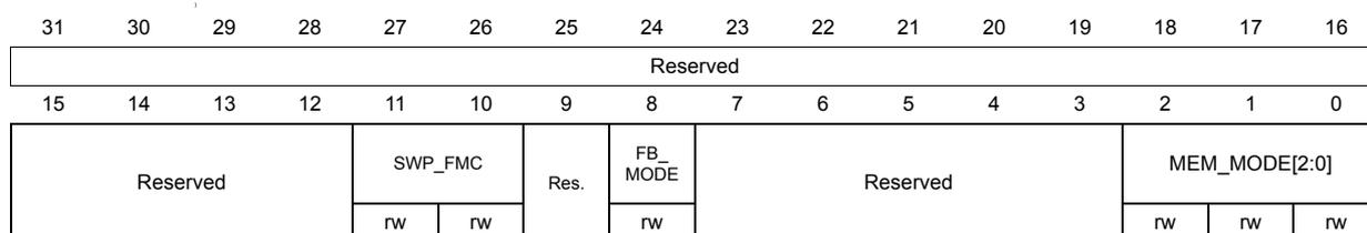
9.3.1 SYSCFG memory remap register (SYSCFG_MEMRMP)
This register is used for specific configurations on memory remap:
- Three bits are used to configure the type of memory accessible at address 0x0000 0000. These bits are used to select the physical remap by software and so, bypass the BOOT pins.
- After reset these bits take the value selected by the BOOT pins. When booting from main Flash memory with BOOT pins set to 10 [(BOOT1,BOOT0) = (1,0)] this register takes the value 0x00.
- Other bits are used to swap FMC SDRAM Bank 1/2 with FMC Bank 3/4 and configure the Flash Bank 1/2 mapping
There are two possible FMC remap at address 0x0000 0000:
- • FMC Bank 1 (NOR/PSRAM 1 and 2) remap:
Only the first two regions of Bank 1 memory controller (Bank1 NOR/PSRAM 1 and NOR/PSRAM 2) can be remapped. - • FMC SDRAM Bank 1 remap.
In remap mode at address 0x0000 0000, the CPU can access the external memory via ICode bus instead of System bus which boosts up the performance.
Address offset: 0x00
Reset value: 0x0000 000X (X is the memory mode selected by the BOOT pins)
Note: Booting from NOR Flash memory or SDRAM is not allowed. The regions can only be mapped at 0x0000 0000 through software remap.
| 31 | 30 | 29 | 28 | 27 | 26 | 25 | 24 | 23 | 22 | 21 | 20 | 19 | 18 | 17 | 16 |
| Reserved | |||||||||||||||
| 15 | 14 | 13 | 12 | 11 | 10 | 9 | 8 | 7 | 6 | 5 | 4 | 3 | 2 | 1 | 0 |
| Reserved | SWP_FMC | Res. | FB_ | Reserved | MEM_MODE[2:0] | ||||||||||
| MODE | rw | rw | rw | ||||||||||||
Bits 31:12 Reserved, must be kept at reset value.
Bits 11:10 SWP_FMC : FMC memory mapping swap
Set and cleared by software. These bits are used to swap the FMC SDRAM Bank 1/2 and FMC Bank 3/4 (SDRAM Bank 1/2 and NAND Bank 2/PCCARD Bank) in order to enable the code execution from SDRAM Banks without a physical remapping at 0x0000 0000 address.
00: No FMC memory mapping swap
01: SDRAM banks and NAND Bank 2/PCCARD mapping are swapped. SDRAM Bank 1 and 2 are mapped at NAND Bank 2 (0x8000 0000) and PCCARD Bank (0x9000 0000) address, respectively. NAND Bank 2 and PCCARD Bank are mapped at 0xC000 0000 and 0xD000 0000, respectively.
10: Reserved
11: Reserved
Bit 9 Reserved, must be kept at reset value.
Bit 8 FB_MODE : Flash Bank mode selection
Set and cleared by software. This bit controls the Flash Bank 1/2 mapping.
0: Flash Bank 1 is mapped at 0x0800 0000 (and aliased at 0x0000 0000) and Flash Bank 2 is mapped at 0x0810 0000 (and aliased at 0x0010 0000)
1: Flash Bank 2 is mapped at 0x0800 0000 (and aliased at 0x0000 0000) and Flash Bank 1 is mapped at 0x0810 0000 (and aliased at 0x0010 0000)
Bits 7:3 Reserved, must be kept at reset value.
Bits 2:0 MEM_MODE : Memory mapping selection
Set and cleared by software. This bit controls the memory internal mapping at address 0x0000 0000. After reset these bits take the value selected by the Boot pins (except for FMC).
000: Main Flash memory mapped at 0x0000 0000
001: System Flash memory mapped at 0x0000 0000
010: FMC Bank1 (NOR/PSRAM 1 and 2) mapped at 0x0000 0000
011: Embedded SRAM (SRAM1) mapped at 0x0000 0000
100: FMC/SDRAM Bank 1 mapped at 0x0000 0000
Other configurations are reserved
Note: Refer to Section 2.3: Memory map for details about the memory mapping at address 0x0000 0000.
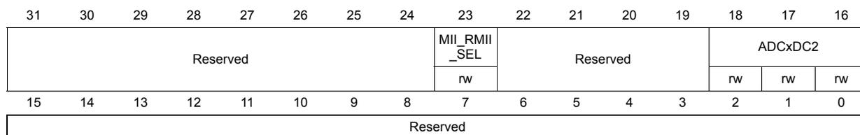
9.3.2 SYSCFG peripheral mode configuration register (SYSCFG_PMC)
Address offset: 0x04
Reset value: 0x0000 0000
| 31 | 30 | 29 | 28 | 27 | 26 | 25 | 24 | 23 | 22 | 21 | 20 | 19 | 18 | 17 | 16 |
| Reserved | MII_RMII _SEL | Reserved | ADCxDC2 | ||||||||||||
| rw | rw | rw | rw | ||||||||||||
| 15 | 14 | 13 | 12 | 11 | 10 | 9 | 8 | 7 | 6 | 5 | 4 | 3 | 2 | 1 | 0 |
| Reserved | |||||||||||||||
Bits 31:24 Reserved, must be kept at reset value.
Bit 23 MII_RMII_SEL : Ethernet PHY interface selection
Set and Cleared by software. These bits control the PHY interface for the Ethernet MAC.
0: MII interface is selected
1: RMII PHY interface is selected
Note: This configuration must be done while the MAC is under reset and before enabling the MAC clocks.
Bits 22:19 Reserved, must be kept at reset value.
Bits 18:16 ADCxDC2:
0: No effect.
1: Refer to AN4073 on how to use this bit.
Note: These bits can be set only if the following conditions are met:
- - ADC clock higher or equal to 30 MHz.
- - Only one ADCxDC2 bit must be selected if ADC conversions do not start at the same time and the sampling times differ.
- - These bits must not be set when the ADCDC1 bit is set in PWR_CR register.
Bits 15:0 Reserved, must be kept at reset value.
9.3.3 SYSCFG external interrupt configuration register 1 (SYSCFG_EXTICR1)
Address offset: 0x08
Reset value: 0x0000 0000
| 31 | 30 | 29 | 28 | 27 | 26 | 25 | 24 | 23 | 22 | 21 | 20 | 19 | 18 | 17 | 16 |
|---|---|---|---|---|---|---|---|---|---|---|---|---|---|---|---|
| Reserved | |||||||||||||||
| 15 | 14 | 13 | 12 | 11 | 10 | 9 | 8 | 7 | 6 | 5 | 4 | 3 | 2 | 1 | 0 |
| EXTI3[3:0] | EXTI2[3:0] | EXTI1[3:0] | EXTI0[3:0] | ||||||||||||
| rw | rw | rw | rw | rw | rw | rw | rw | rw | rw | rw | rw | rw | rw | rw | rw |
Bits 31:16 Reserved, must be kept at reset value.
Bits 15:0 EXTIx[3:0]: EXTI x configuration (x = 0 to 3)
These bits are written by software to select the source input for the EXTIx external interrupt.
- 0000: PA[x] pin
- 0001: PB[x] pin
- 0010: PC[x] pin
- 0011: PD[x] pin
- 0100: PE[x] pin
- 0101: PF[x] pin
- 0110: PG[x] pin
- 0111: PH[x] pin
- 1000: PI[x] pin
- 1001: PJ[x] pin
- 1010: PK[x] pin
9.3.4 SYSCFG external interrupt configuration register 2 (SYSCFG_EXTICR2)
Address offset: 0x0C
Reset value: 0x0000 0000
| 31 | 30 | 29 | 28 | 27 | 26 | 25 | 24 | 23 | 22 | 21 | 20 | 19 | 18 | 17 | 16 |
| Reserved | |||||||||||||||
| 15 | 14 | 13 | 12 | 11 | 10 | 9 | 8 | 7 | 6 | 5 | 4 | 3 | 2 | 1 | 0 |
| EXTI7[3:0] | EXTI6[3:0] | EXTI5[3:0] | EXTI4[3:0] | ||||||||||||
| rw | rw | rw | rw | rw | rw | rw | rw | rw | rw | rw | rw | rw | rw | rw | rw |
Bits 31:16 Reserved, must be kept at reset value.
Bits 15:0 EXTIx[3:0] : EXTI x configuration (x = 4 to 7)
These bits are written by software to select the source input for the EXTIx external interrupt.
- 0000: PA[x] pin
- 0001: PB[x] pin
- 0010: PC[x] pin
- 0011: PD[x] pin
- 0100: PE[x] pin
- 0101: PF[x] pin
- 0110: PG[x] pin
- 0111: PH[x] pin
- 1000: PI[x] pin
- 1001: PJ[x] pin
- 1010: PK[x] pin
9.3.5 SYSCFG external interrupt configuration register 3 (SYSCFG_EXTICR3)
Address offset: 0x10
Reset value: 0x0000 0000
| 31 | 30 | 29 | 28 | 27 | 26 | 25 | 24 | 23 | 22 | 21 | 20 | 19 | 18 | 17 | 16 |
| Reserved | |||||||||||||||
| 15 | 14 | 13 | 12 | 11 | 10 | 9 | 8 | 7 | 6 | 5 | 4 | 3 | 2 | 1 | 0 |
| EXTI11[3:0] | EXTI10[3:0] | EXTI9[3:0] | EXTI8[3:0] | ||||||||||||
| rw | rw | rw | rw | rw | rw | rw | rw | rw | rw | rw | rw | rw | rw | rw | rw |
Bits 31:16 Reserved, must be kept at reset value.
Bits 15:0 EXTIx[3:0] : EXTI x configuration (x = 8 to 11)
These bits are written by software to select the source input for the EXTIx external interrupt.
0000: PA[x] pin
0001: PB[x] pin
0010: PC[x] pin
0011: PD[x] pin
0100: PE[x] pin
0101: PF[x] pin
0110: PG[x] pin
0111: PH[x] pin
1000: PI[x] pin
1001: PJ[x] pin
Note: PK[11:8] are not used.
9.3.6 SYSCFG external interrupt configuration register 4 (SYSCFG_EXTICR4)
Address offset: 0x14
Reset value: 0x0000 0000
| 31 | 30 | 29 | 28 | 27 | 26 | 25 | 24 | 23 | 22 | 21 | 20 | 19 | 18 | 17 | 16 |
|---|---|---|---|---|---|---|---|---|---|---|---|---|---|---|---|
| Reserved | |||||||||||||||
| 15 | 14 | 13 | 12 | 11 | 10 | 9 | 8 | 7 | 6 | 5 | 4 | 3 | 2 | 1 | 0 |
| EXTI15[3:0] | EXTI14[3:0] | EXTI13[3:0] | EXTI12[3:0] | ||||||||||||
| rw | rw | rw | rw | rw | rw | rw | rw | rw | rw | rw | rw | rw | rw | rw | rw |
Bits 31:16 Reserved, must be kept at reset value.
Bits 15:0 EXTIx[3:0] : EXTI x configuration (x = 12 to 15)
These bits are written by software to select the source input for the EXTIx external interrupt.
0000: PA[x] pin
0001: PB[x] pin
0010: PC[x] pin
0011: PD[x] pin
0100: PE[x] pin
0101: PF[x] pin
0110: PG[x] pin
0111: PH[x] pin
1000: PI[x] pin
1001: PJ[x] pin
Note: PK[15:12] are not used.
9.3.7 Compensation cell control register (SYSCFG_CMPCR)
Address offset: 0x20
Reset value: 0x0000 0000
| 31 | 30 | 29 | 28 | 27 | 26 | 25 | 24 | 23 | 22 | 21 | 20 | 19 | 18 | 17 | 16 | |
| Reserved | ||||||||||||||||
| 15 | 14 | 13 | 12 | 11 | 10 | 9 | 8 | 7 | 6 | 5 | 4 | 3 | 2 | 1 | 0 | |
| Reserved | READY | Reserved | CMP_PD | |||||||||||||
| r | rw | |||||||||||||||
Bits 31:9 Reserved, must be kept at reset value.
Bit 8 READY : Compensation cell ready flag
0: I/O compensation cell not ready
1: O compensation cell ready
Bits 7:2 Reserved, must be kept at reset value.
Bit 0 CMP_PD : Compensation cell power-down
0: I/O compensation cell power-down mode
1: I/O compensation cell enabled
9.3.8 SYSCFG register maps for STM32F42xxx and STM32F43xxx
The following table gives the SYSCFG register map and the reset values.
Table 42. SYSCFG register map and reset values (STM32F42xxx and STM32F43xxx)
| Offset | Register | 31 | 30 | 29 | 28 | 27 | 26 | 25 | 24 | 23 | 22 | 21 | 20 | 19 | 18 | 17 | 16 | 15 | 14 | 13 | 12 | 11 | 10 | 9 | 8 | 7 | 6 | 5 | 4 | 3 | 2 | 1 | 0 |
|---|---|---|---|---|---|---|---|---|---|---|---|---|---|---|---|---|---|---|---|---|---|---|---|---|---|---|---|---|---|---|---|---|---|
| 0x00 | SYSCFG_MEMRMP | Reserved | SWP_FMC | Reserved | FB_MODE | Reserved | MEM MODE | x | x | x | |||||||||||||||||||||||
| Reset value | 0 | 0 | |||||||||||||||||||||||||||||||
| 0x04 | SYSCFG_PMC | Reserved | MII_RMII_SEL | Reserved | ADC3DC2 | ADC2DC2 | ADC1DC2 | Reserved | |||||||||||||||||||||||||
| Reset value | 0 | 0 | 0 | 0 | |||||||||||||||||||||||||||||
| 0x08 | SYSCFG_EXTICR1 | Reserved | EXTI3[3:0] | EXTI2[3:0] | EXTI1[3:0] | EXTI0[3:0] | |||||||||||||||||||||||||||
| Reset value | 0 | 0 | 0 | 0 | 0 | 0 | 0 | 0 | 0 | 0 | |||||||||||||||||||||||
| 0x0C | SYSCFG_EXTICR2 | Reserved | EXTI7[3:0] | EXTI6[3:0] | EXTI5[3:0] | EXTI4[3:0] | |||||||||||||||||||||||||||
| Reset value | 0 | 0 | 0 | 0 | 0 | 0 | 0 | 0 | 0 | 0 | |||||||||||||||||||||||
| 0x10 | SYSCFG_EXTICR3 | Reserved | EXTI11[3:0] | EXTI10[3:0] | EXTI9[3:0] | EXTI8[3:0] | |||||||||||||||||||||||||||
| Reset value | 0 | 0 | 0 | 0 | 0 | 0 | 0 | 0 | 0 | 0 | |||||||||||||||||||||||
| 0x14 | SYSCFG_EXTICR4 | Reserved | EXTI15[3:0] | EXTI14[3:0] | EXTI13[3:0] | EXTI12[3:0] | |||||||||||||||||||||||||||
| Reset value | 0 | 0 | 0 | 0 | 0 | 0 | 0 | 0 | 0 | 0 | |||||||||||||||||||||||
| 0x20 | SYSCFG_CMPCR | Reserved | READY | Reserved | CMP _PD | 0 | |||||||||||||||||||||||||||
| Reset value | 0 | ||||||||||||||||||||||||||||||||
Refer to Section 2.3: Memory map for the register boundary addresses.