3. Embedded flash memory interface
3.1 Introduction
The flash memory interface manages CPU AHB I-Code and D-Code accesses to the flash memory. It implements the erase and program flash memory operations and the read and write protection mechanisms.
The flash memory interface accelerates code execution with a system of instruction prefetch and cache lines.
3.2 Main features
- • Flash memory read operations
- • Flash memory program/erase operations
- • Read / write protections
- • Prefetch on I-Code
- • 64 cache lines of 128 bits on I-Code
- • 8 cache lines of 128 bits on D-Code
Figure 3 shows the flash memory interface connection inside the system architecture.
Figure 3. Flash memory interface connection inside system architecture
(STM32F405xx/07xx and STM32F415xx/17xx)
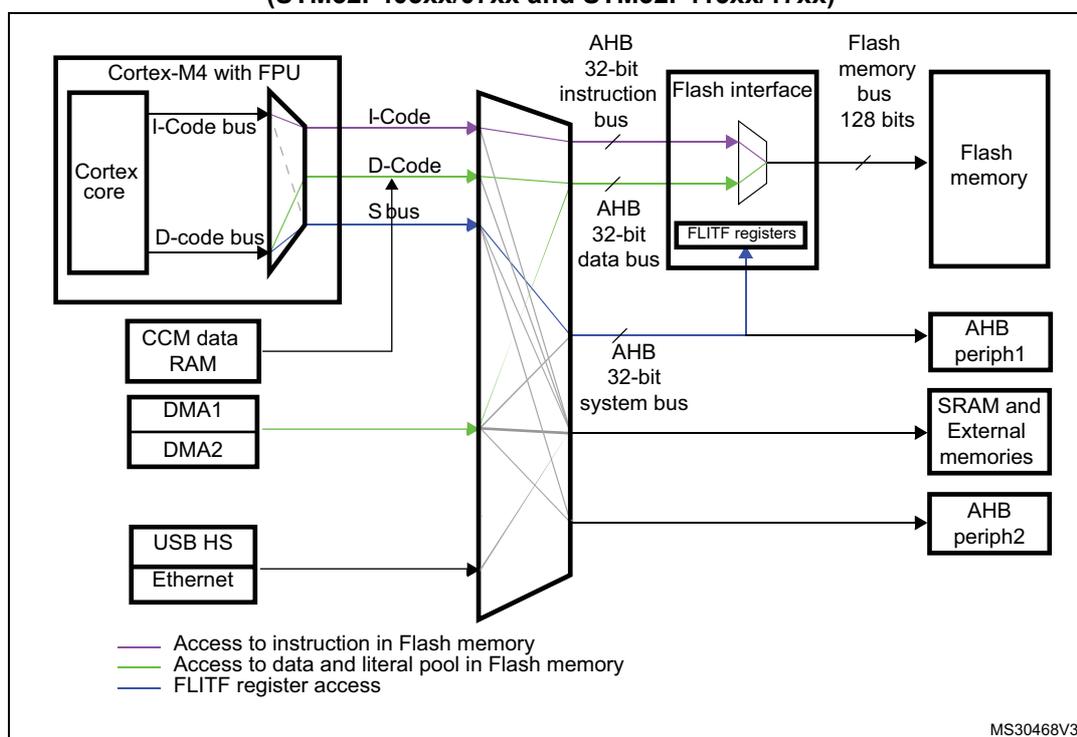
The diagram illustrates the system architecture for STM32F405xx/07xx and STM32F415xx/17xx microcontrollers. At the center is the Cortex-M4 with FPU block, which contains a Cortex core . This core is connected to a central AHB 32-bit system bus via several interfaces: an I-Code bus (purple line), a D-Code bus (green line), and an S bus (blue line). The I-Code bus connects to the Flash interface block, which in turn connects to the Flash memory via a Flash memory bus 128 bits . The D-Code bus connects to the Flash interface and also to the CCM data RAM block. The S bus connects to the Flash interface and also to the FLITF registers block within the Flash interface . The CCM data RAM block is also connected to the AHB 32-bit system bus . The FLITF registers block is connected to the Flash interface and also to the AHB 32-bit system bus . The AHB 32-bit system bus is connected to several other blocks: DMA1 , DMA2 , USB HS , Ethernet , AHB periph1 , SRAM and External memories , and AHB periph2 . A legend at the bottom left indicates the color coding for the bus connections: purple for Access to instruction in Flash memory , green for Access to data and literal pool in Flash memory , and blue for FLITF register access . The diagram is labeled with the reference number MS30468V3 in the bottom right corner.
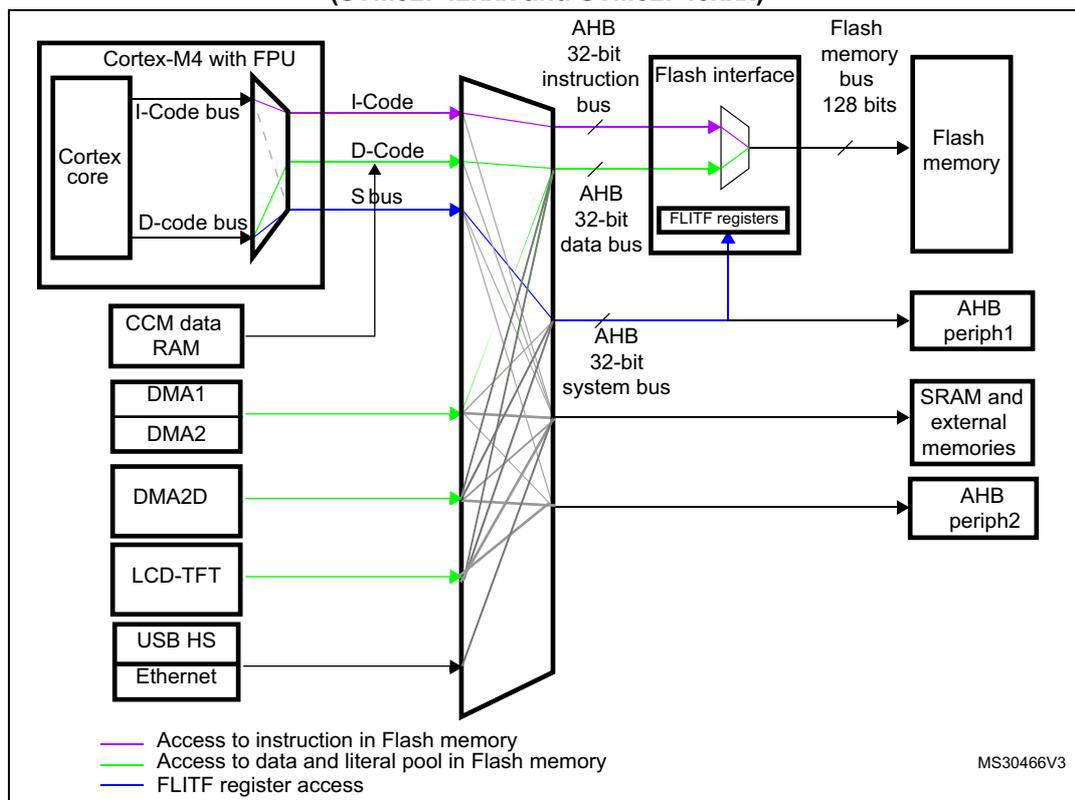
Figure 4. Flash memory interface connection inside system architecture (STM32F42xxx and STM32F43xxx)
3.3 Embedded flash memory in STM32F405xx/07xx and STM32F415xx/17xx
The flash memory has the following main features:
- • Capacity up to 1 Mbyte
- • 128 bits wide data read
- • Byte, half-word, word and double word write
- • Sector and mass erase
- • Memory organization
The flash memory is organized as follows:
- – A main memory block divided into 4 sectors of 16 Kbytes, 1 sector of 64 Kbytes, and 7 sectors of 128 Kbytes
- – System memory from which the device boots in System memory boot mode
- – 512 OTP (one-time programmable) bytes for user data
The OTP area contains 16 additional bytes used to lock the corresponding OTP data block.
- – Option bytes to configure read and write protection, BOR level, watchdog software/hardware and reset when the device is in Standby or Stop mode.
- • Low-power modes (for details refer to the Power control (PWR) section of the reference manual)
| Block | Name | Block base addresses | Size |
|---|---|---|---|
| Main memory | Sector 0 | 0x0800 0000 - 0x0800 3FFF | 16 Kbytes |
| Sector 1 | 0x0800 4000 - 0x0800 7FFF | 16 Kbytes | |
| Sector 2 | 0x0800 8000 - 0x0800 BFFF | 16 Kbytes | |
| Sector 3 | 0x0800 C000 - 0x0800 FFFF | 16 Kbytes | |
| Sector 4 | 0x0801 0000 - 0x0801 FFFF | 64 Kbytes | |
| Sector 5 | 0x0802 0000 - 0x0803 FFFF | 128 Kbytes | |
| Sector 6 | 0x0804 0000 - 0x0805 FFFF | 128 Kbytes | |
| . | . | . | |
| . | . | . | |
| Sector 11 | 0x080E 0000 - 0x080F FFFF | 128 Kbytes | |
| System memory | 0x1FFF 0000 - 0x1FFF 77FF | 30 Kbytes | |
| OTP area | 0x1FFF 7800 - 0x1FFF 7A0F | 528 bytes | |
| Option bytes | 0x1FFF C000 - 0x1FFF C00F | 16 bytes | |
3.4 Embedded flash memory in STM32F42xxx and STM32F43xxx
The flash memory has the following main features:
- • Capacity up to 2 Mbyte with dual bank architecture supporting read-while-write capability (RWW)
- • 128 bits wide data read
- • Byte, half-word, word and double word write
- • Sector, bank, and mass erase (both banks)
- • Dual bank memory organization
The dual bank organization is available only on 1 Mbyte and 2 Mbyte devices.
The flash memory is organized as follows:
- – For each bank, a main memory block (1 Mbyte) divided into 4 sectors of 16 Kbytes, 1 sector of 64 Kbytes, and 7 sectors of 128 Kbytes
- – System memory from which the device boots in System memory boot mode
- – 512 OTP (one-time programmable) bytes for user data
The OTP area contains 16 additional bytes used to lock the corresponding OTP data block.
- – Option bytes to configure read and write protection, BOR level, watchdog, dual bank boot mode, dual bank feature, software/hardware and reset when the device is in Standby or Stop mode.
- • Dual bank organization on 1 Mbyte devices
The dual bank feature on 1 Mbyte devices is enabled by setting the DB1M option bit.
To obtain a dual bank flash memory, the last 512 Kbytes of the single bank (sectors [8:11]) are re-structured in the same way as the first 512 Kbytes.
The sector numbering of dual bank memory organization is different from the single bank: the single bank memory contains 12 sectors whereas the dual bank memory contains 16 sectors (see Table 7: 1 Mbyte flash memory single bank vs dual bank organization (STM32F42xxx and STM32F43xxx) ).
For erase operation, the right sector numbering must be considered according the DB1M option bit.
- – When the DB1M bit is reset, the erase operation must be performed on the default sector number.
- – When the DB1M bit is set, to perform an erase operation on bank 2, the sector number must be programmed (sector number from 12 to 19). Refer to FLASH_CR register for SNB (Sector number) configuration.
Refer to Table 8: 1 Mbyte single bank flash memory organization (STM32F42xxx and STM32F43xxx) and Table 9: 1 Mbyte dual bank flash memory organization (STM32F42xxx and STM32F43xxx) for details on 1 Mbyte single bank and 1 Mbyte dual bank organizations.
Table 6. Flash module - 2 Mbyte dual bank organization (STM32F42xxx and STM32F43xxx)
| Block | Bank | Name | Block base addresses | Size |
|---|---|---|---|---|
| Main memory | Bank 1 | Sector 0 | 0x0800 0000 - 0x0800 3FFF | 16 Kbytes |
| Sector 1 | 0x0800 4000 - 0x0800 7FFF | 16 Kbytes | ||
| Sector 2 | 0x0800 8000 - 0x0800 BFFF | 16 Kbytes | ||
| Sector 3 | 0x0800 C000 - 0x0800 FFFF | 16 Kbyte | ||
| Sector 4 | 0x0801 0000 - 0x0801 FFFF | 64 Kbytes | ||
| Sector 5 | 0x0802 0000 - 0x0803 FFFF | 128 Kbytes | ||
| Sector 6 | 0x0804 0000 - 0x0805 FFFF | 128 Kbytes | ||
| . | - | - | ||
| . | - | - | ||
| - | - | - | ||
| Sector 11 | 0x080E 0000 - 0x080F FFFF | 128 Kbytes | ||
| Bank 2 | Sector 12 | 0x0810 0000 - 0x0810 3FFF | 16 Kbytes | |
| Sector 13 | 0x0810 4000 - 0x0810 7FFF | 16 Kbytes | ||
| Sector 14 | 0x0810 8000 - 0x0810 BFFF | 16 Kbytes | ||
| Sector 15 | 0x0810 C000 - 0x0810 FFFF | 16 Kbytes | ||
| Sector 16 | 0x0811 0000 - 0x0811 FFFF | 64 Kbytes | ||
| Sector 17 | 0x0812 0000 - 0x0813 FFFF | 128 Kbytes | ||
| Sector 18 | 0x0814 0000 - 0x0815 FFFF | 128 Kbytes | ||
| . | . | . | ||
| . | . | . | ||
| . | . | . | ||
| Sector 23 | 0x081E 0000 - 0x081F FFFF | 128 Kbytes | ||
| System memory | 0x1FFF 0000 - 0x1FFF 77FF | 30 Kbytes | ||
| OTP | 0x1FFF 7800 - 0x1FFF 7A0F | 528 bytes | ||
| Option bytes | Bank 1 | 0x1FFF C000 - 0x1FFF C00F | 16 bytes | |
| Bank 2 | 0x1FFE C000 - 0x1FFE C00F | 16 bytes | ||
Table 7. 1 Mbyte flash memory single bank vs dual bank organization
(STM32F42xxx and STM32F43xxx)
| 1 Mbyte single bank flash memory (default) | 1 Mbyte dual bank flash memory | ||||
|---|---|---|---|---|---|
| DB1M=0 | DB1M=1 | ||||
| Main memory | Sector number | Sector size | Main memory | Sector number | Sector size |
| 1MB | Sector 0 | 16 Kbytes | Bank 1 512KB | Sector 0 | 16 Kbytes |
| Sector 1 | 16 Kbytes | Sector 1 | 16 Kbytes | ||
| Sector 2 | 16 Kbytes | Sector 2 | 16 Kbytes | ||
| Sector 3 | 16 Kbytes | Sector 3 | 16 Kbytes | ||
| Sector 4 | 64 Kbytes | Sector 4 | 64 Kbytes | ||
| Sector 5 | 128 Kbytes | Sector 5 | 128 Kbytes | ||
| Sector 6 | 128 Kbytes | Sector 6 | 128 Kbytes | ||
| Sector 7 | 128 Kbytes | Sector 7 | 128 Kbytes | ||
| Sector 8 | 128 Kbytes | Bank 2 512KB | Sector 12 | 16 Kbytes | |
| Sector 9 | 128 Kbytes | Sector 13 | 16 Kbytes | ||
| Sector 10 | 128 Kbytes | Sector 14 | 16 Kbytes | ||
| Sector 11 | 128 Kbytes | Sector 15 | 16 Kbytes | ||
| - | - | Sector 16 | 64 Kbytes | ||
| - | - | Sector 17 | 128 Kbytes | ||
| - | - | Sector 18 | 128 Kbytes | ||
| - | - | Sector 19 | 128 Kbytes | ||
Table 8. 1 Mbyte single bank flash memory organization
(STM32F42xxx and STM32F43xxx)
| Block | Bank | Name | Block base addresses | Size |
|---|---|---|---|---|
| Main memory | Single bank | Sector 0 | 0x0800 0000 - 0x0800 3FFF | 16 Kbytes |
| Sector 1 | 0x0800 4000 - 0x0800 7FFF | 16 Kbytes | ||
| Sector 2 | 0x0800 8000 - 0x0800 BFFF | 16 Kbytes | ||
| Sector 3 | 0x0800 C000 - 0x0800 FFFF | 16 Kbytes | ||
| Sector 4 | 0x0801 0000 - 0x0801 FFFF | 64 Kbytes | ||
| Sector 5 | 0x0802 0000 - 0x0803 FFFF | 128 Kbytes | ||
| Sector 6 | 0x0804 0000 - 0x0805 FFFF | 128 Kbytes | ||
| Sector 7 | 0x0806 0000 - 0x0807 FFFF | 128 Kbytes | ||
| Sector 8 | 0x0808 0000 - 0x0809 FFFF | 128 Kbytes | ||
| Sector 9 | 0x080A 0000 - 0x080B FFFF | 128 Kbytes | ||
| Sector 10 | 0x080C 0000 - 0x080D FFFF | 128 Kbytes | ||
| Sector 11 | 0x080E 0000 - 0x080F FFFF | 128 Kbytes |
Table 8. 1 Mbyte single bank flash memory organization
(STM32F42xxx and STM32F43xxx) (continued)
| Block | Bank | Name | Block base addresses | Size |
|---|---|---|---|---|
| System memory | 0x1FFF 0000 - 0x1FFFF 77FF | 30 Kbytes | ||
| OTP | 0x1FFF 7800 - 0x1FFF 7A0F | 528 bytes | ||
| Option bytes | 0x1FFF C000 - 0x1FFF C00F | 16 bytes | ||
| 0x1FFE C000 - 0x1FFE C00F | 16 bytes | |||
Table 9. 1 Mbyte dual bank flash memory organization (STM32F42xxx and STM32F43xxx)
| Block | Bank | Name | Block base addresses | Size |
|---|---|---|---|---|
| Main memory | Bank 1 | Sector 0 | 0x0800 0000 - 0x0800 3FFF | 16 Kbytes |
| Sector 1 | 0x0800 4000 - 0x0800 7FFF | 16 Kbytes | ||
| Sector 2 | 0x0800 8000 - 0x0800 BFFF | 16 Kbytes | ||
| Sector 3 | 0x0800 C000 - 0x0800 FFFF | 16 Kbyte | ||
| Sector 4 | 0x0801 0000 - 0x0801 FFFF | 64 Kbytes | ||
| Sector 5 | 0x0802 0000 - 0x0803 FFFF | 128 Kbytes | ||
| Sector 6 | 0x0804 0000 - 0x0805 FFFF | 128 Kbytes | ||
| Sector 7 | 0x0806 0000 - 0x0807 FFFF | 128 Kbytes | ||
| Bank 2 | Sector 12 | 0x0808 0000 - 0x0808 3FFF | 16 Kbytes | |
| Sector 13 | 0x0808 4000 - 0x0808 7FFF | 16 Kbytes | ||
| Sector 14 | 0x0808 8000 - 0x0808 BFFF | 16 Kbytes | ||
| Sector 15 | 0x0808 C000 - 0x0808 FFFF | 16 Kbytes | ||
| Sector 16 | 0x0809 0000 - 0x0809 FFFF | 64 Kbytes | ||
| Sector 17 | 0x080A 0000 - 0x080B FFFF | 128 Kbytes | ||
| Sector 18 | 0x080C 0000 - 0x080D FFFF | 128 Kbytes | ||
| Sector 19 | 0x080E 0000 - 0x080F FFFF | 128 Kbytes | ||
| System memory | 0x1FFF 0000 - 0x1FFF 77FF | 30 Kbytes | ||
| OTP | 0x1FFF 7800 - 0x1FFF 7A0F | 528 bytes | ||
| Option bytes | Bank 1 | 0x1FFF C000 - 0x1FFF C00F | 16 bytes | |
| Bank 2 | 0x1FFE C000 - 0x1FFE C00F | 16 bytes | ||
Table 10. 512 Kbyte single bank flash memory organization
(STM32F42xxx and STM32F43xxx)
| Block | Bank | Name | Block base addresses | Size |
|---|---|---|---|---|
| Main memory | Single Bank | Sector 0 | 0x0800 0000 - 0x0800 3FFF | 16 Kbytes |
| Sector 1 | 0x0800 4000 - 0x0800 7FFF | 16 Kbytes | ||
| Sector 2 | 0x0800 8000 - 0x0800 BFFF | 16 Kbytes | ||
| Sector 3 | 0x0800 C000 - 0x0800 FFFF | 16 Kbytes | ||
| Sector 4 | 0x0801 0000 - 0x0801 FFFF | 64 Kbytes | ||
| Sector 5 | 0x0802 0000 - 0x0803 FFFF | 128 Kbytes | ||
| Sector 6 | 0x0804 0000 - 0x0805 FFFF | 128 Kbytes | ||
| Sector 7 | 0x0806 0000 - 0x0807 FFFF | 128 Kbytes | ||
| System memory | 0x1FFF 0000 - 0x1FFFF 77FF | 30 Kbytes | ||
| OTP | 0x1FFF 7800 - 0x1FFF 7A0F | 528 bytes | ||
| Option bytes | 0x1FFF C000 - 0x1FFF C00F | 16 bytes | ||
| 0x1FFE C000 - 0x1FFE C00F | 16 bytes | |||
3.5 Read interface
3.5.1 Relation between CPU clock frequency and flash memory read time
To correctly read data from flash memory, the number of wait states (LATENCY) must be correctly programmed in the Flash access control register (FLASH_ACR) according to the frequency of the CPU clock (HCLK) and the supply voltage of the device.
The prefetch buffer must be disabled when the supply voltage is below 2.1 V. The correspondence between wait states and CPU clock frequency is given in Table 11 and Table 12 .
Note: On STM32F405xx/07xx and STM32F415xx/17xx devices:
- - when VOS = '0', the maximum value of \( f_{HCLK} \) = 144 MHz.
- - when VOS = '1', the maximum value of \( f_{HCLK} \) = 168 MHz.
On STM32F42xxx and STM32F43xxx devices:
- - when VOS[1:0] = '0x01', the maximum value of \( f_{HCLK} \) is 120 MHz.
- - when VOS[1:0] = '0x10', the maximum value of \( f_{HCLK} \) is 144 MHz. It can be extended to 168 MHz by activating the over-drive mode.
- - when VOS[1:0] = '0x11', the maximum value of \( f_{HCLK} \) is 168 MHz. It can be extended to 180 MHz by activating the over-drive mode.
- - The over-drive mode is not available when \( V_{DD} \) ranges from 1.8 to 2.1 V.
Refer to Section 5.1.4: Voltage regulator for STM32F42xxx and STM32F43xxx for details on how to activate the over-drive mode.
Table 11. Number of wait states according to CPU clock (HCLK) frequency
(STM32F405xx/07xx and STM32F415xx/17xx)
| Wait states (WS) (LATENCY) | HCLK (MHz) | |||
|---|---|---|---|---|
| Voltage range 2.7 V - 3.6 V | Voltage range 2.4 V - 2.7 V | Voltage range 2.1 V - 2.4 V | Voltage range 1.8 V - 2.1 V Prefetch OFF | |
| 0 WS (1 CPU cycle) | \( 0 < HCLK \leq 30 \) | \( 0 < HCLK \leq 24 \) | \( 0 < HCLK \leq 22 \) | \( 0 < HCLK \leq 20 \) |
| 1 WS (2 CPU cycles) | \( 30 < HCLK \leq 60 \) | \( 24 < HCLK \leq 48 \) | \( 22 < HCLK \leq 44 \) | \( 20 < HCLK \leq 40 \) |
| 2 WS (3 CPU cycles) | \( 60 < HCLK \leq 90 \) | \( 48 < HCLK \leq 72 \) | \( 44 < HCLK \leq 66 \) | \( 40 < HCLK \leq 60 \) |
| 3 WS (4 CPU cycles) | \( 90 < HCLK \leq 120 \) | \( 72 < HCLK \leq 96 \) | \( 66 < HCLK \leq 88 \) | \( 60 < HCLK \leq 80 \) |
| 4 WS (5 CPU cycles) | \( 120 < HCLK \leq 150 \) | \( 96 < HCLK \leq 120 \) | \( 88 < HCLK \leq 110 \) | \( 80 < HCLK \leq 100 \) |
| 5 WS (6 CPU cycles) | \( 150 < HCLK \leq 168 \) | \( 120 < HCLK \leq 144 \) | \( 110 < HCLK \leq 132 \) | \( 100 < HCLK \leq 120 \) |
| 6 WS (7 CPU cycles) | - | \( 144 < HCLK \leq 168 \) | \( 132 < HCLK \leq 154 \) | \( 120 < HCLK \leq 140 \) |
| 7 WS (8 CPU cycles) | - | - | \( 154 < HCLK \leq 168 \) | \( 140 < HCLK \leq 160 \) |
Table 12. Number of wait states according to CPU clock (HCLK) frequency
(STM32F42xxx and STM32F43xxx)
| Wait states (WS) (LATENCY) | HCLK (MHz) | |||
|---|---|---|---|---|
| Voltage range 2.7 V - 3.6 V | Voltage range 2.4 V - 2.7 V | Voltage range 2.1 V - 2.4 V | Voltage range 1.8 V - 2.1 V Prefetch OFF | |
| 0 WS (1 CPU cycle) | \( 0 < HCLK \leq 30 \) | \( 0 < HCLK \leq 24 \) | \( 0 < HCLK \leq 22 \) | \( 0 < HCLK \leq 20 \) |
| 1 WS (2 CPU cycles) | \( 30 < HCLK \leq 60 \) | \( 24 < HCLK \leq 48 \) | \( 22 < HCLK \leq 44 \) | \( 20 < HCLK \leq 40 \) |
| 2 WS (3 CPU cycles) | \( 60 < HCLK \leq 90 \) | \( 48 < HCLK \leq 72 \) | \( 44 < HCLK \leq 66 \) | \( 40 < HCLK \leq 60 \) |
| 3 WS (4 CPU cycles) | \( 90 < HCLK \leq 120 \) | \( 72 < HCLK \leq 96 \) | \( 66 < HCLK \leq 88 \) | \( 60 < HCLK \leq 80 \) |
| 4 WS (5 CPU cycles) | \( 120 < HCLK \leq 150 \) | \( 96 < HCLK \leq 120 \) | \( 88 < HCLK \leq 110 \) | \( 80 < HCLK \leq 100 \) |
| 5 WS (6 CPU cycles) | \( 150 < HCLK \leq 180 \) | \( 120 < HCLK \leq 144 \) | \( 110 < HCLK \leq 132 \) | \( 100 < HCLK \leq 120 \) |
| 6 WS (7 CPU cycles) | - | \( 144 < HCLK \leq 168 \) | \( 132 < HCLK \leq 154 \) | \( 120 < HCLK \leq 140 \) |
| 7 WS (8 CPU cycles) | - | \( 168 < HCLK \leq 180 \) | \( 154 < HCLK \leq 176 \) | \( 140 < HCLK \leq 160 \) |
| 8 WS (9 CPU cycles) | - | - | \( 176 < HCLK \leq 180 \) | \( 160 < HCLK \leq 168 \) |
After reset, the CPU clock frequency is 16 MHz and 0 wait state (WS) is configured in the FLASH_ACR register.
It is highly recommended to use the following software sequences to tune the number of wait states needed to access the flash memory with the CPU frequency.
Increasing the CPU frequency
- 1. Program the new number of wait states to the LATENCY bits in the FLASH_ACR register
- 2. Check that the new number of wait states is taken into account to access the flash memory by reading the FLASH_ACR register
- 3. Modify the CPU clock source by writing the SW bits in the RCC_CFGR register
- 4. If needed, modify the CPU clock prescaler by writing the HPRE bits in RCC_CFGR
- 5. Check that the new CPU clock source or/and the new CPU clock prescaler value is/are taken into account by reading the clock source status (SWS bits) or/and the AHB prescaler value (HPRE bits), respectively, in the RCC_CFGR register.
Decreasing the CPU frequency
- 1. Modify the CPU clock source by writing the SW bits in the RCC_CFGR register
- 2. If needed, modify the CPU clock prescaler by writing the HPRE bits in RCC_CFGR
- 3. Check that the new CPU clock source or/and the new CPU clock prescaler value is/are taken into account by reading the clock source status (SWS bits) or/and the AHB prescaler value (HPRE bits), respectively, in the RCC_CFGR register
- 4. Program the new number of wait states to the LATENCY bits in FLASH_ACR
- 5. Check that the new number of wait states is used to access the flash memory by reading the FLASH_ACR register
Note: A change in CPU clock configuration or wait state (WS) configuration may not be effective straight away. To make sure that the current CPU clock frequency is the one you have configured, you can check the AHB prescaler factor and clock source status values. To make sure that the number of WS you have programmed is effective, you can read the FLASH_ACR register.
3.5.2 Adaptive real-time memory accelerator (ART Accelerator™)
The proprietary Adaptive real-time (ART) memory accelerator is optimized for STM32 industry-standard Arm® Cortex®-M4 with FPU processors. It balances the inherent performance advantage of the Arm® Cortex®-M4 with FPU over flash memory technologies, which normally requires the processor to wait for the flash memory at higher operating frequencies.
To release the processor full performance, the accelerator implements an instruction prefetch queue and branch cache which increases program execution speed from the 128-bit flash memory. Based on CoreMark benchmark, the performance achieved thanks to the ART accelerator is equivalent to 0 wait state program execution from flash memory at a CPU frequency up to 180 MHz.
Instruction prefetch
Each flash memory read operation provides 128 bits from either four instructions of 32 bits or 8 instructions of 16 bits according to the program launched. So, in case of sequential code, at least four CPU cycles are needed to execute the previous read instruction line. Prefetch on the I-Code bus can be used to read the next sequential instruction line from the flash memory while the current instruction line is being requested by the CPU. Prefetch is enabled by setting the PRFTEN bit in the FLASH_ACR register. This feature is useful if at least one wait state is needed to access the flash memory.
Figure 5 shows the execution of sequential 32-bit instructions with and without prefetch when 3 WSs are needed to access the flash memory.
Figure 5. Sequential 32-bit instruction execution
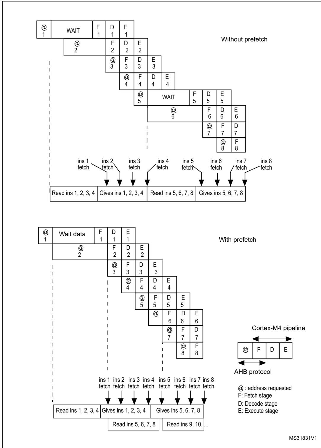
Without prefetch
| @ 1 | WAIT | F 1 | D 1 | E 1 | ||||
| @ 2 | F 2 | D 2 | E 2 | |||||
| @ 3 | F 3 | D 3 | E 3 | |||||
| @ 4 | F 4 | D 4 | E 4 | |||||
| @ 5 | WAIT | F 5 | D 5 | E 5 | ||||
| @ 6 | F 6 | D 6 | E 6 | |||||
| @ 7 | F 7 | D 7 | ||||||
| @ 8 | F 8 |
ins 1 fetch ins 2 fetch ins 3 fetch ins 4 fetch ins 5 fetch ins 6 fetch ins 7 fetch ins 8 fetch
| Read ins 1, 2, 3, 4 | Gives ins 1, 2, 3, 4 | Read ins 5, 6, 7, 8 | Gives ins 5, 6, 7, 8 |
With prefetch
| @ 1 | Wait data | F 1 | D 1 | E 1 | ||||
| @ 2 | F 2 | D 2 | E 2 | |||||
| @ 3 | F 3 | D 3 | E 3 | |||||
| @ 4 | F 4 | D 4 | E 4 | |||||
| @ 5 | F 5 | D 5 | E 5 | |||||
| @ 6 | F 6 | D 6 | E 6 | |||||
| @ 7 | F 7 | D 7 | ||||||
| @ 8 | F 8 |
ins 1 fetch ins 2 fetch ins 3 fetch ins 4 fetch ins 5 fetch ins 6 fetch ins 7 fetch ins 8 fetch
| Read ins 1, 2, 3, 4 | Gives ins 1, 2, 3, 4 | Gives ins 5, 6, 7, 8 | Read ins 9, 10, ... |
| Read ins 5, 6, 7, 8 |
Cortex-M4 pipeline
| @ | F | D | E |
AHB protocol
@ : address requested
F: Fetch stage
D: Decode stage
E: Execute stage
MS31831V1
When the code is not sequential (branch), the instruction may not be present in the currently used instruction line or in the prefetched instruction line. In this case (miss), the penalty in terms of number of cycles is at least equal to the number of wait states.
Instruction cache memory
To limit the time lost due to jumps, it is possible to retain 64 lines of 128 bits in an instruction cache memory. This feature can be enabled by setting the instruction cache enable (ICEN) bit in the FLASH_ACR register. Each time a miss occurs (requested data not present in the currently used instruction line, in the prefetched instruction line or in the instruction cache memory), the line read is copied into the instruction cache memory. If some data contained in the instruction cache memory are requested by the CPU, they are provided without inserting any delay. Once all the instruction cache memory lines have been filled, the LRU (least recently used) policy is used to determine the line to replace in the instruction memory cache. This feature is particularly useful in case of code containing loops.
Data management
Literal pools are fetched from flash memory through the D-Code bus during the execution stage of the CPU pipeline. The CPU pipeline is consequently stalled until the requested literal pool is provided. To limit the time lost due to literal pools, accesses through the AHB databus D-Code have priority over accesses through the AHB instruction bus I-Code.
If some literal pools are frequently used, the data cache memory can be enabled by setting the data cache enable (DCEN) bit in the FLASH_ACR register. This feature works like the instruction cache memory, but the retained data size is limited to 8 rows of 128 bits.
Note: Data in user configuration sector are not cacheable.
3.6 Erase and program operations
For any flash memory program operation (erase or program), the CPU clock frequency (HCLK) must be at least 1 MHz. The contents of the flash memory are not guaranteed if a device reset occurs during a flash memory operation.
Any attempt to read the flash memory on STM32F4xx while it is being written or erased, causes the bus to stall. Read operations are processed correctly once the program operation has completed. This means that code or data fetches cannot be performed while a write/erase operation is ongoing.
On STM32F42xxx and STM32F43xxx devices, two banks are available allowing read operation from one bank while a write/erase operation is performed to the other bank.
3.6.1 Unlocking the Flash control register
After reset, write is not allowed in the Flash control register (FLASH_CR) to protect the flash memory against possible unwanted operations due, for example, to electric disturbances. The following sequence is used to unlock this register:
- 1. Write KEY1 = 0x45670123 in the Flash key register (FLASH_KEYR)
- 2. Write KEY2 = 0xCDEF89AB in the Flash key register (FLASH_KEYR)
Any wrong sequence returns a bus error and lock up the FLASH_CR register until the next reset.
The FLASH_CR register can be locked again by software by setting the LOCK bit in the FLASH_CR register.
Note: The FLASH_CR register is not accessible in write mode when the BSY bit in the FLASH_SR register is set. Any attempt to write to it with the BSY bit set causes the AHB bus to stall until the BSY bit is cleared.
3.6.2 Program/erase parallelism
The parallelism size is configured through the PSIZE field in the FLASH_CR register. It represents the number of bytes to be programmed each time a write operation occurs to the flash memory. PSIZE is limited by the supply voltage and by whether the external V PP supply is used or not. It must therefore be correctly configured in the FLASH_CR register before any programming/erasing operation.
A flash memory erase operation can only be performed by sector, bank or for the whole flash memory (mass erase). The erase time depends on PSIZE programmed value. For more details on the erase time, refer to the electrical characteristics section of the device datasheet.
Table 13 provides the correct maximum PSIZE values.
Table 13. Maximum program/erase parallelism
| Voltage range 2.7 - 3.6 V with External V PP | Voltage range 2.7 - 3.6 V | Voltage range 2.4 - 2.7 V | Voltage range 2.1 - 2.4 V | Voltage range 1.8 V - 2.1 V | |
|---|---|---|---|---|---|
| Max. parallelism size | x64 | x32 | x16 | x16 | x8 |
| PSIZE(1:0) | 11 | 10 | 01 | 01 | 00 |
Note: Any program or erase operation started with inconsistent program parallelism/voltage range settings may lead to unpredicted results. Even if a subsequent read operation indicates that the logical value was effectively written to the memory, this value may not be retained.
To use V PP , an external high-voltage supply (between 8 and 9 V) must be applied to the V PP pad. The external supply must be able to sustain this voltage range even if the DC consumption exceeds 10 mA. It is advised to limit the use of V PP to initial programming on the factory line. The V PP supply must not be applied for more than an hour, otherwise the flash memory might be damaged.
3.6.3 Erase
The flash memory erase operation can be performed at sector level or on the whole flash memory (Mass Erase). Mass Erase does not affect the OTP sector or the configuration sector.
Sector Erase
To erase a sector, follow the procedure below:
- 1. Check that no flash memory operation is ongoing by checking the BSY bit in the FLASH_SR register
- 2. Set the SER bit and select the sector out of the 12 sectors (for STM32F405xx/07xx and STM32F415xx/17xx) and out of 24 (for STM32F42xxx and STM32F43xxx) in the main memory block you wish to erase (SNB) in the FLASH_CR register
- 3. Set the STRT bit in the FLASH_CR register
- 4. Wait for the BSY bit to be cleared
Bank erase in STM32F42xxx and STM32F43xxx devices
To erase bank 1 or bank 2, follow the procedure below:
- 1. Check that no flash memory operation is ongoing by checking the BSY bit in the FLASH_SR register
- 2. Set MER or MER1 bit accordingly in the FLASH_CR register
- 3. Set the STRT bit in the FLASH_CR register
- 4. Wait for the BSY bit to be reset.
Mass Erase
To perform Mass Erase, the following sequence is recommended:
- 1. Check that no flash memory operation is ongoing by checking the BSY bit in the FLASH_SR register
- 2. Set the MER bit in the FLASH_CR register (on STM32F405xx/07xx and STM32F415xx/17xx devices)
- 3. Set both the MER and MER1 bits in the FLASH_CR register (on STM32F42xxx and STM32F43xxx devices).
- 4. Set the STRT bit in the FLASH_CR register
- 5. Wait for the BSY bit to be cleared
Note: If MERx and SER bits are both set in the FLASH_CR register, mass erase is performed. If both MERx and SER bits are reset and the STRT bit is set, an unpredictable behavior may occur without generating any error flag. This condition should be forbidden.
3.6.4 Programming
Standard programming
The flash memory programming sequence is as follows:
- 1. Check that no main flash memory operation is ongoing by checking the BSY bit in the FLASH_SR register.
- 2. Set the PG bit in the FLASH_CR register
- 3. Perform the data write operation(s) to the desired memory address (inside main memory block or OTP area):
- – Byte access in case of x8 parallelism
- – Half-word access in case of x16 parallelism
- – Word access in case of x32 parallelism
- – Double word access in case of x64 parallelism
- 4. Wait for the BSY bit to be cleared.
Note:
Successive write operations are possible without the need of an erase operation when changing bits from '1' to '0'. Writing '1' requires a flash memory erase operation.
If an erase and a program operation are requested simultaneously, the erase operation is performed first.
Programming errors
It is not allowed to program data to the flash memory that would cross the 128-bit row boundary. In such a case, the write operation is not performed and a program alignment error flag (PGAERR) is set in the FLASH_SR register.
The write access type (byte, half-word, word or double word) must correspond to the type of parallelism chosen (x8, x16, x32 or x64). If not, the write operation is not performed and a program parallelism error flag (PGPERR) is set in the FLASH_SR register.
If the standard programming sequence is not respected (for example, if there is an attempt to write to a flash memory address when the PG bit is not set), the operation is aborted and a program sequence error flag (PGSERR) is set in the FLASH_SR register.
Programming and caches
If a flash memory write access concerns some data in the data cache, the Flash write access modifies the data in the flash memory and the data in the cache.
If an erase operation in flash memory also concerns data in the data or instruction cache, you have to make sure that these data are rewritten before they are accessed during code execution. If this cannot be done safely, it is recommended to flush the caches by setting the DCRST and ICRST bits in the FLASH_CR register.
Note: The I/D cache should be flushed only when it is disabled (I/DCEN = 0).
3.6.5 Read-while-write (RWW)
In STM32F42xxx and STM32F43xxx devices, the flash memory is divided into two banks allowing read-while-write operations. This feature allows to perform a read operation from one bank while an erase or program operation is performed to the other bank.
Note: Write-while-write operations are not allowed. As an example, it is not possible to perform an erase operation on one bank while programming the other one.
Read from bank 1 while erasing bank 2
While executing a program code from bank 1, it is possible to perform an erase operation on bank 2 (and vice versa). Follow the procedure below:
- 1. Check that no flash memory operation is ongoing by checking the BSY bit in the FLASH_SR register (BSY is active when erase/program operation is ongoing to bank 1 or bank 2)
- 2. Set MER or MER1 bit in the FLASH_CR register
- 3. Set the STRT bit in the FLASH_CR register
- 4. Wait for the BSY bit to be reset (or use the EOP interrupt).
Read from bank 1 while programming bank 2
While executing a program code (over the I-Code bus) from bank 1, it is possible to perform an program operation to the bank 2 (and vice versa). Follow the procedure below:
- 1. Check that no flash memory operation is ongoing by checking the BSY bit in the FLASH_SR register (BSY is active when erase/program operation is on going on bank 1 or bank 2)
- 2. Set the PG bit in the FLASH_CR register
- 3. Perform the data write operation(s) to the desired memory address inside main memory block or OTP area
- 4. Wait for the BSY bit to be reset.
3.6.6 Interrupts
Setting the end of operation interrupt enable bit (EOPIE) in the FLASH_CR register enables interrupt generation when an erase or program operation ends, that is when the busy bit (BSY) in the FLASH_SR register is cleared (operation completed, correctly or not). In this case, the end of operation (EOP) bit in the FLASH_SR register is set.
If an error occurs during a program, an erase, or a read operation request, one of the following error flags is set in the FLASH_SR register:
- • PGAERR, PGPERR, PGSERR (Program error flags)
- • WRPERR (Protection error flag)
- • RDERR (Read protection error flag) for STM32F42xxx and STM32F43xxx devices only.
In this case, if the error interrupt enable bit (ERRIE) is set in the FLASH_CR register, an interrupt is generated and the operation error bit (OPERR) is set in the FLASH_SR register.
Note: If several successive errors are detected (for example, in case of DMA transfer to the flash memory), the error flags cannot be cleared until the end of the successive write requests.
Table 14. Flash interrupt request
| Interrupt event | Event flag | Enable control bit |
|---|---|---|
| End of operation | EOP | EOPIE |
| Write protection error | WRPERR | ERRIE |
| Programming error | PGAERR, PGPERR, PGSERR | ERRIE |
| Read protection error | RDERR | ERRIE |
3.7 Option bytes
3.7.1 Description of user option bytes
The option bytes are configured by the end user depending on the application requirements. Table 15 shows the organization of these bytes inside the user configuration sector.
Table 15. Option byte organization
| Address | [63:16] | [15:0] |
|---|---|---|
| 0x1FFF C000 | Reserved | ROP & user option bytes ( RDP & USER ) |
| 0x1FFF C008 | Reserved | SPRMOD and Write protection nWRP bits for sectors 0 to 11 |
Table 15. Option byte organization (continued)
| Address | [63:16] | [15:0] |
|---|---|---|
| 0x1FFE C000 | Reserved | Reserved |
| 0x1FFE C008 | Reserved | SPRMOD and Write protection nWRP bits for sectors 12 to 23 |
Table 16. Description of the option bytes (STM32F405xx/07xx and STM32F415xx/17xx)
| Option bytes (word, address 0x1FFF C000) | |
|---|---|
| RDP:
Read protection option byte. The read protection is used to protect the software code stored in flash memory. | |
| Bits 15:8 | 0xAA: Level 0, no protection 0xCC: Level 2, chip protection (debug and boot from RAM features disabled) Others: Level 1, read protection of memories (debug features limited) |
| USER:
User option byte This byte is used to configure the following features: – Select the watchdog event: Hardware or software – Reset event when entering the Stop mode – Reset event when entering the Standby mode | |
| Bit 7 | nRST_STDBY 0: Reset generated when entering the Standby mode 1: No reset generated |
| Bit 6 | nRST_STOP 0: Reset generated when entering the Stop mode 1: No reset generated |
| Bit 5 | WDG_SW 0: Hardware independent watchdog 1: Software independent watchdog |
| Bit 4 | 0x1: Not used |
| Bits 3:2 | BOR_LEV:
BOR reset Level These bits contain the supply level threshold that activates/releases the reset. They can be written to program a new BOR level value into flash memory. 00: BOR Level 3 (VBOR3), brownout threshold level 3 01: BOR Level 2 (VBOR2), brownout threshold level 2 10: BOR Level 1 (VBOR1), brownout threshold level 1 11: BOR off, POR/PDR reset threshold level is applied Note: For full details on BOR characteristics, refer to the “Electrical characteristics” section of the product datasheet. |
| Bits 1:0 | 0x3: Not used |
| Option bytes (word, address 0x1FFF C008) | |
|---|---|
| Bits 15:12 | 0xF: Not used |
| nWRP:
Flash memory write protection option bytes Sectors 0 to 11 can be write protected. | |
| Bits 11:0 | nWRPi 0: Write protection active on selected sector 1: Write protection not active on selected sector |
| Option bytes (word, address 0x1FFF C000) | |
|---|---|
| RDP:
Read protection option byte. The read protection is used to protect the software code stored in flash memory. | |
| Bit 15:8 | 0xAA: Level 0, no protection 0xCC: Level 2, chip protection (debug and boot from RAM features disabled) Others: Level 1, read protection of memories (debug features limited) |
| USER:
User option byte This byte is used to configure the following features: Select the watchdog event: Hardware or software Reset event when entering the Stop mode Reset event when entering the Standby mode | |
| Bit 7 | nRST_STDBY 0: Reset generated when entering the Standby mode 1: No reset generated |
| Bit 6 | nRST_STOP 0: Reset generated when entering the Stop mode 1: No reset generated |
| Bit 5 | WDG_SW 0: Hardware independent watchdog 1: Software independent watchdog |
| Bit 4 | BFB2:
Dual bank boot 0: Boot from flash memory bank 1 or system memory depending on boot pin state (Default). 1: Boot always from system memory (Dual bank boot mode). |
Table 17. Description of the option bytes
(STM32F42xxx and STM32F43xxx) (continued)
| Bits 3:2 | BOR_LEV:
BOR reset Level These bits contain the supply level threshold that activates/releases the reset. They can be written to program a new BOR level value into flash memory. 00: BOR Level 3 (VBOR3), brownout threshold level 3 01: BOR Level 2 (VBOR2), brownout threshold level 2 10: BOR Level 1 (VBOR1), brownout threshold level 1 11: BOR off, POR/PDR reset threshold level is applied Note: For full details on BOR characteristics, refer to the “Electrical characteristics” section of the product datasheet. |
| Bits 1:0 | 0x3: Not used |
| Option bytes (word, address 0x1FFF C008) | |
| Bit 15 | SPRMOD:
Selection of protection mode of nWPRI bits 0: nWPRI bits used for sector i write protection (Default) 1: nWPRI bits used for sector i PCROP protection (Sector) |
| Bit 14 | DB1M:
Dual bank 1 Mbyte flash memory devices 0: 1 Mbyte single flash memory (contiguous addresses in bank 1) 1: 1 Mbyte dual bank flash memory. The flash memory is organized as two banks of 512 Kbytes each (see Table 7: 1 Mbyte flash memory single bank vs dual bank organization (STM32F42xxx and STM32F43xxx) and Table 9: 1 Mbyte dual bank flash memory organization (STM32F42xxx and STM32F43xxx) ). To perform an erase operation, the right sector must be programmed (see Table 7 for information on the sector numbering scheme). |
| Bits 13:12 | 0x3: not used |
| nWRP: Flash memory write protection option bytes for bank 1. Sectors 0 to 11 can be write protected. | |
| Bits 11:0 | nWRPi: If SPRMOD is reset (default value): 0: Write protection active on sector i. 1: Write protection not active on sector i. If SPRMOD is set (active): 0: PCROP protection not active on sector i. 1: PCROP protection active on sector i. |
| Option bytes (word, address 0x1FFE C000) | |
| Bit 15:0 | 0xFFFF: not used |
Table 17. Description of the option bytes
(STM32F42xxx and STM32F43xxx) (continued)
| Option bytes (word, address 0x1FFE C008) | |
|---|---|
| Bit 15:12 | 0xF: not used |
| nWRP: Flash memory write protection option bytes for bank 2. Sectors 12 to 23 can be write protected. | |
| Bits 11: 0 | nWRPi: If SPRMOD is reset (default value): 0: Write protection active on sector i. 1: Write protection not active on sector i. If SPRMOD is set (active): 0: PCROP protection not active on sector i. 1: PCROP protection active on sector i. |
3.7.2 Programming user option bytes
To run any operation on this sector, the option lock bit (OPTLOCK) in the Flash option control register (FLASH_OPTCR) must be cleared. To be allowed to clear this bit, you have to perform the following sequence:
- 1. Write OPTKEY1 = 0x0819 2A3B in the Flash option key register (FLASH_OPTKEYR)
- 2. Write OPTKEY2 = 0x4C5D 6E7F in the Flash option key register (FLASH_OPTKEYR)
The user option bytes can be protected against unwanted erase/program operations by setting the OPTLOCK bit by software.
Modifying user option bytes on STM32F405xx/07xx and STM32F415xx/17xx
To modify the user option value, follow the sequence below:
- 1. Check that no flash memory operation is ongoing by checking the BSY bit in the FLASH_SR register
- 2. Write the desired option value in the FLASH_OPTCR register.
- 3. Set the option start bit (OPTSTRT) in the FLASH_OPTCR register
- 4. Wait for the BSY bit to be cleared.
Note: The value of an option is automatically modified by first erasing the user configuration sector and then programming all the option bytes with the values contained in the FLASH_OPTCR register.
Modifying user option bytes on STM32F42xxx and STM32F43xxx
The user option bytes for bank 1 and bank 2 cannot be modified independently. They must be updated concurrently.
To modify the user option byte value, follow the sequence below:
- 1. Check that no flash memory operation is ongoing by checking the BSY bit in the FLASH_SR register
- 2. Write the bank 2 option byte value in the FLASH_OPTCR1 register
- 3. Write the bank 1 option byte value in the FLASH_OPTCR register.
- 4. Set the option start bit (OPTSTRT) in the FLASH_OPTCR register
- 5. Wait for the BSY bit to be cleared
Note: The value of an option byte is automatically modified by first erasing the user configuration sector (bank 1 and 2) and then programming all the option bytes with the values contained in the FLASH_OPTCR and FLASH_OPTCR1 registers.
3.7.3 Read protection (RDP)
The user area in the flash memory can be protected against read operations by an entrusted code. Three read protection levels are defined:
- • Level 0: no read protection
When the read protection level is set to Level 0 by writing 0xAA into the read protection option byte (RDP), all read/write operations (if no write protection is set) from/to the flash memory or the backup SRAM are possible in all boot configurations (Flash user boot, debug or boot from RAM).
- • Level 1: read protection enabled
It is the default read protection level after option byte erase. The read protection Level 1 is activated by writing any value (except for 0xAA and 0xCC used to set Level 0 and Level 2, respectively) into the RDP option byte. When the read protection Level 1 is set:
- – No access (read, erase, program) to flash memory or backup SRAM can be performed while the debug feature is connected or while booting from RAM or system memory bootloader. A bus error is generated in case of read request.
- – When booting from flash memory, accesses (read, erase, program) to flash memory and backup SRAM from user code are allowed.
When Level 1 is active, programming the protection option byte (RDP) to Level 0 causes the flash memory and the backup SRAM to be mass-erased. As a result the user code area is cleared before the read protection is removed. The mass erase only erases the user code area. The other option bytes including write protections remain unchanged from before the mass-erase operation. The OTP area is not affected by mass erase and remains unchanged. Mass erase is performed only when Level 1 is active and Level 0 requested. When the protection level is increased (0->1, 1->2, 0->2) there is no mass erase.
- • Level 2: debug/chip read protection disabled
The read protection Level 2 is activated by writing 0xCC to the RDP option byte. When the read protection Level 2 is set:
- – All protections provided by Level 1 are active.
- – Booting from RAM or system memory bootloader is no more allowed.
- – JTAG, SWV (single-wire viewer), ETM, and boundary scan are disabled.
- – User option bytes can no longer be changed.
- – When booting from flash memory, accesses (read, erase and program) to flash memory and backup SRAM from user code are allowed.
Memory read protection Level 2 is an irreversible operation. When Level 2 is activated, the level of protection cannot be decreased to Level 0 or Level 1.
Note:
If the read protection is set while the debugger is still connected (or has been connected since the last power-on) through JTAG/SWD, apply a POR (power-on reset) instead of a system reset.
If the read protection is programmed by software (executing from SRAM), perform a POR to reload the option byte and clear the detected intrusion. This can be done with a transition Standby mode followed by a wake-up.
The JTAG port is permanently disabled when Level 2 is active (acting as a JTAG fuse). As a consequence, boundary scan cannot be performed. STMicroelectronics is not able to perform analysis on defective parts on which the Level 2 protection has been set.
Table 18. Access versus read protection level
| Memory area | Protection Level | Debug features, Boot from RAM or from System memory bootloader | Booting from flash memory | ||||
|---|---|---|---|---|---|---|---|
| Read | Write | Erase | Read | Write | Erase | ||
| Main Flash Memory and Backup SRAM | Level 1 | NO | NO (1) | YES | |||
| Level 2 | NO | YES | |||||
| Option Bytes | Level 1 | YES | YES | ||||
| Level 2 | NO | NO | |||||
| OTP | Level 1 | NO | NA | YES | NA | ||
| Level 2 | NO | NA | YES | NA | |||
- 1. The main flash memory and backup SRAM are only erased when the RDP changes from level 1 to 0. The OTP area remains unchanged.
Figure 6 shows how to go from one RDP level to another.
Figure 6. RDP levels
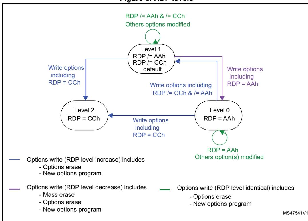
The diagram illustrates the transitions between three RDP (Read Protection) levels:
- Level 1 (Center): RDP ≠ AAh & ≠ CCh (default). Includes a green self-loop for "RDP ≠ AAh & ≠ CCh Others options modified".
- Level 2 (Left): RDP = CCh.
- Level 0 (Right): RDP = AAh. Includes a green self-loop for "RDP = AAh Others option(s) modified".
Transitions:
- Level 1 to Level 2 : Blue arrow labeled "Write options including RDP = CCh".
- Level 0 to Level 1 : Blue arrow labeled "Write options including RDP ≠ CCh & ≠ AAh".
- Level 0 to Level 2 : Blue arrow labeled "Write options including RDP = CCh".
- Level 1 to Level 0 : Purple arrow labeled "Write options including RDP = AAh".
- Level 2 to Level 1 : Purple arrow labeled "Write options including RDP ≠ AAh & ≠ CCh".
- Level 2 to Level 0 : Purple arrow labeled "Write options including RDP = AAh".
Legend:
- —
Options write (RDP level increase) includes:
- - Options erase
- - New options program
- —
Options write (RDP level decrease) includes:
- - Mass erase
- - Options erase
- - New options program
- —
Options write (RDP level identical) includes:
- - Options erase
- - New options program
MS47541V1
3.7.4 Write protections
Up to 24 user sectors in flash memory can be protected against unwanted write operations due to loss of program counter contexts. When the non-write protection nWRPi bit ( \( 0 \le i \le 11 \) ) in the FLASH_OPTCR or FLASH_OPTCR1 registers is low, the corresponding sector
cannot be erased or programmed. Consequently, a mass erase cannot be performed if one of the sectors is write-protected.
If an erase/program operation to a write-protected part of the flash memory is attempted (sector protected by write protection bit, OTP part locked or part of the flash memory that can never be written like the ICP), the write protection error flag (WRPERR) is set in the FLASH_SR register.
On STM32F42xxx and STM32F43xxx devices, when the PCROP mode is set, the active level of nWRPi is high, and the corresponding sector i is write protected when nWRPi is high. A PCROP sector is automatically write protected.
Note: When the memory read protection level is selected (RDP level = 1), it is not possible to program or erase flash memory sector i if the CPU debug features are connected (JTAG or single wire) or boot code is being executed from RAM, even if nWRPi = 1.
Write protection error flag
If an erase/program operation to a write protected area of the flash memory is performed, the Write Protection Error flag (WRPERR) is set in the FLASH_SR register.
If an erase operation is requested, the WRPERR bit is set when:
- • Mass, bank, sector erase are configured (MER or MER/MER1 and SER = 1)
- • A sector erase is requested and the Sector Number SNB field is not valid
- • A mass erase is requested while at least one of the user sector is write protected by option bit (MER or MER/MER1 = 1 and nWRPi = 0 with \( 0 \leq i \leq 11 \) bits in the FLASH_OPTCRx register)
- • A sector erase is requested on a write protected sector. (SER = 1, SNB = i and nWRPi = 0 with \( 0 \leq i \leq 11 \) bits in the FLASH_OPTCRx register)
- • The flash memory is readout protected and an intrusion is detected.
If a program operation is requested, the WRPERR bit is set when:
- • A write operation is performed on system memory or on the reserved part of the user specific sector.
- • A write operation is performed to the user configuration sector
- • A write operation is performed on a sector write protected by option bit.
- • A write operation is requested on an OTP area which is already locked
- • The flash memory is read protected and an intrusion is detected.
3.7.5 Proprietary code readout protection (PCROP)
The proprietary readout protection (PCROP) is available only on STM32F42xxx and STM32F43xxx devices.
Flash memory user sectors (0 to 23) can be protected against D-bus read accesses by using the proprietary readout protection (PCROP).
The PCROP protection is selected as follows, through the SPRMOD option bit in the FLASH_OPTCR register:
- • SPRMOD = 0: nWRPi control the write protection of respective user sectors
- • SPRMOD = 1: nWRPi control the read and write protection (PCROP) of respective user sectors.
When a sector is readout protected (PCROP mode activated), it can only be accessed for code fetch through ICODE Bus on Flash interface:
- • Any read access performed through the D-bus triggers a RDERR flag error.
- • Any program/erase operation on a PCROPed sector triggers a WRPERR flag error.
Figure 7. PCROP levels
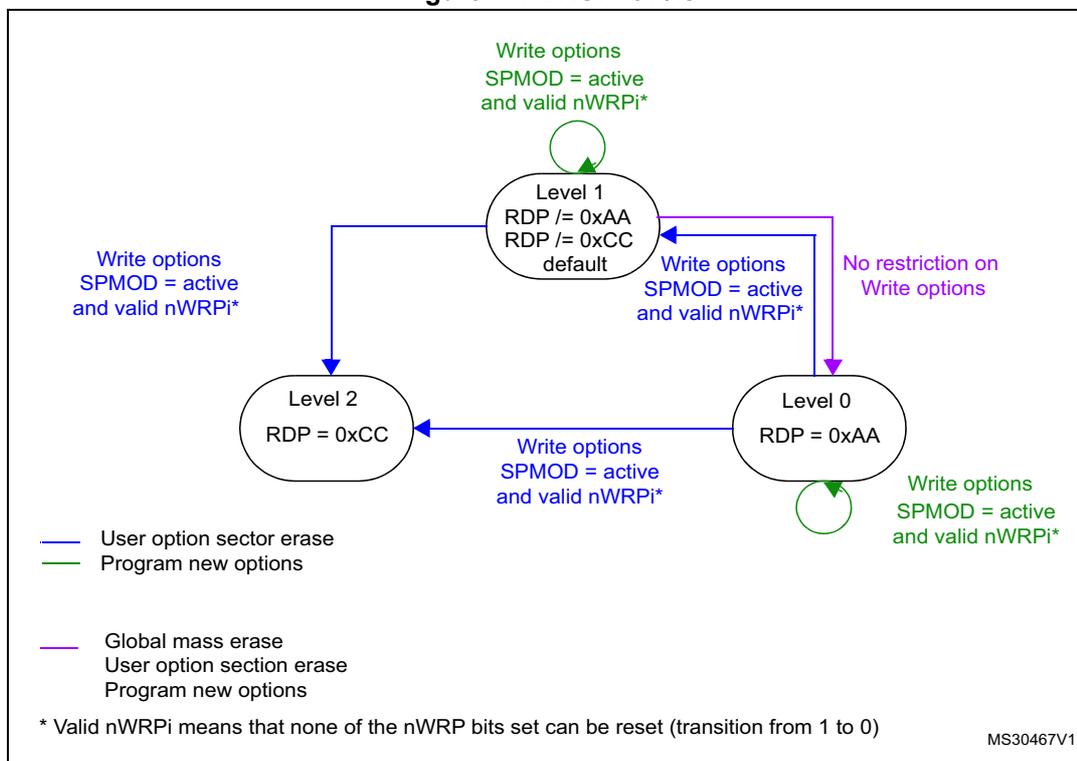
The diagram illustrates three states of PCROP protection:
- Level 1 (default): Defined by RDP ≠ 0xAA and RDP ≠ 0xCC. Transitions to Level 2 occur via 'User option sector erase' when SPMOD is active and nWRPi is valid. Transitions to Level 0 occur via 'Global mass erase', 'User option section erase', or 'Program new options' when SPMOD is active and nWRPi is valid.
- Level 0: Defined by RDP = 0xAA. Transitions to Level 1 occur via 'Program new options' with no restriction on write options. Transitions to Level 2 occur via 'User option sector erase' when SPMOD is active and nWRPi is valid.
- Level 2: Defined by RDP = 0xCC. This is a terminal state for RDP, but the diagram shows a transition to Level 1 via 'Program new options' when SPMOD is active and nWRPi is valid.
Legend:
—
User option sector erase
—
Program new options
—
Global mass erase, User option section erase, Program new options
* Valid nWRPi means that none of the nWRP bits set can be reset (transition from 1 to 0)
MS30467V1
The deactivation of the SPMOD and/or the unprotection of PCROPed user sectors can only occur when, at the same time, the RDP level changes from 1 to 0. If this condition is not respected, the user option byte modification is cancelled and the write error WRPERR flag is set. The modification of the users option bytes (BOR_LEV, RST_STDBY, ..) is allowed since none of the active nWRPi bits is reset and SPMOD is kept active.
Note:
The active value of nWRPi bits is inverted when PCROP mode is active (SPRMOD = 1).
If SPRMOD = 1 and nWRPi = 1, then user sector i of bank 1, respectively bank 2 is read/write protected (PCROP).
3.8 One-time programmable bytes
Table 19 shows the organization of the one-time programmable (OTP) part of the OTP area.
Table 19. OTP area organization
| Block | [128:96] | [95:64] | [63:32] | [31:0] | Address byte 0 |
|---|---|---|---|---|---|
| 0 | OTP0 | OTP0 | OTP0 | OTP0 | 0x1FFF 7800 |
| OTP0 | OTP0 | OTP0 | OTP0 | 0x1FFF 7810 | |
| 1 | OTP1 | OTP1 | OTP1 | OTP1 | 0x1FFF 7820 |
| OTP1 | OTP1 | OTP1 | OTP1 | 0x1FFF 7830 | |
| . | . | ||||
| . | . | ||||
| . | . | ||||
| 15 | OTP15 | OTP15 | OTP15 | OTP15 | 0x1FFF 79E0 |
| OTP15 | OTP15 | OTP15 | OTP15 | 0x1FFF 79F0 | |
| Lock block | LOCKB15 ... LOCKB12 | LOCKB11 ... LOCKB8 | LOCKB7 ... LOCKB4 | LOCKB3 ... LOCKB0 | 0x1FFF 7A00 |
The OTP area is divided into 16 OTP data blocks of 32 bytes and one lock OTP block of 16 bytes. The OTP data and lock blocks cannot be erased. The lock block contains 16 bytes LOCKBi ( \( 0 \leq i \leq 15 \) ) to lock the corresponding OTP data block (blocks 0 to 15). Each OTP data block can be programmed until the value 0x00 is programmed in the corresponding OTP lock byte. The lock bytes must only contain 0x00 and 0xFF values, otherwise the OTP bytes might not be taken into account correctly.
3.9 Flash interface registers
3.9.1 Flash access control register (FLASH_ACR)
for STM32F405xx/07xx and STM32F415xx/17xx
The Flash access control register is used to enable/disable the acceleration features and control the flash memory access time according to CPU frequency.
Address offset: 0x00
Reset value: 0x0000 0000
Access: no wait state, word, half-word and byte access
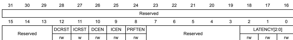
| 31 | 30 | 29 | 28 | 27 | 26 | 25 | 24 | 23 | 22 | 21 | 20 | 19 | 18 | 17 | 16 | |
| Reserved | ||||||||||||||||
| 15 | 14 | 13 | 12 | 11 | 10 | 9 | 8 | 7 | 6 | 5 | 4 | 3 | 2 | 1 | 0 | |
| Reserved | DCRST | ICRST | DCEN | ICEN | PRFTEN | Reserved | LATENCY[2:0] | |||||||||
| rw | w | rw | rw | rw | rw | rw | rw | |||||||||
Bits 31:13 Reserved, must be kept cleared.
Bit 12 DCRST : Data cache reset
0: Data cache is not reset
1: Data cache is reset
This bit can be written only when the D cache is disabled.
Bit 11 ICRST : Instruction cache reset
0: Instruction cache is not reset
1: Instruction cache is reset
This bit can be written only when the I cache is disabled.
Bit 10 DCEN : Data cache enable
0: Data cache is disabled
1: Data cache is enabled
Bit 9 ICEN : Instruction cache enable
0: Instruction cache is disabled
1: Instruction cache is enabled
Bit 8 PRFTEN : Prefetch enable
0: Prefetch is disabled
1: Prefetch is enabled
Bits 7:3 Reserved, must be kept cleared.
Bits 2:0 LATENCY[2:0] : Latency
These bits represent the ratio of the CPU clock period to the flash memory access time.
000: Zero wait state
001: One wait state
010: Two wait states
011: Three wait states
100: Four wait states
101: Five wait states
110: Six wait states
111: Seven wait states
3.9.2 Flash access control register (FLASH_ACR) for STM32F42xxx and STM32F43xxx
The Flash access control register is used to enable/disable the acceleration features and control the flash memory access time according to CPU frequency.
Address offset: 0x00
Reset value: 0x0000 0000
Access: no wait state, word, half-word and byte access
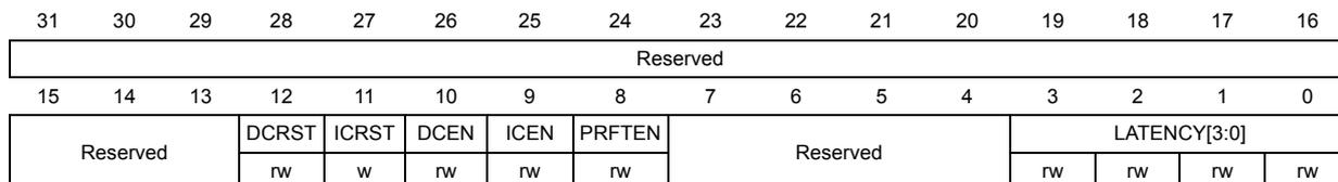
| 31 | 30 | 29 | 28 | 27 | 26 | 25 | 24 | 23 | 22 | 21 | 20 | 19 | 18 | 17 | 16 |
| Reserved | |||||||||||||||
| 15 | 14 | 13 | 12 | 11 | 10 | 9 | 8 | 7 | 6 | 5 | 4 | 3 | 2 | 1 | 0 |
| Reserved | DCRST | ICRST | DCEN | ICEN | PRFTEN | Reserved | LATENCY[3:0] | ||||||||
| rw | w | rw | rw | rw | rw | rw | rw | rw | |||||||
Bits 31:13 Reserved, must be kept cleared.
Bit 12 DCRST : Data cache reset
0: Data cache is not reset
1: Data cache is reset
This bit can be written only when the D cache is disabled.
Bit 11 ICRST : Instruction cache reset
0: Instruction cache is not reset
1: Instruction cache is reset
This bit can be written only when the I cache is disabled.
Bit 10 DCEN : Data cache enable
0: Data cache is disabled
1: Data cache is enabled
Bit 9 ICEN : Instruction cache enable
0: Instruction cache is disabled
1: Instruction cache is enabled
Bit 8 PRFTEN : Prefetch enable
0: Prefetch is disabled
1: Prefetch is enabled
Bits 7:4 Reserved, must be kept cleared.
Bits 3:0 LATENCY[3:0] : Latency
These bits represent the ratio of the CPU clock period to the flash memory access time.
0000: Zero wait state
0001: One wait state
0010: Two wait states
...
1110: Fourteen wait states
1111: Fifteen wait states
3.9.3 Flash key register (FLASH_KEYR)
The Flash key register is used to allow access to the Flash control register and so, to allow program and erase operations.
Address offset: 0x04
Reset value: 0x0000 0000
Access: no wait state, word access

| 31 | 30 | 29 | 28 | 27 | 26 | 25 | 24 | 23 | 22 | 21 | 20 | 19 | 18 | 17 | 16 |
| KEY[31:16] | |||||||||||||||
| w | w | w | w | w | w | w | w | w | w | w | w | w | w | w | w |
| 15 | 14 | 13 | 12 | 11 | 10 | 9 | 8 | 7 | 6 | 5 | 4 | 3 | 2 | 1 | 0 |
| KEY[15:0] | |||||||||||||||
| w | w | w | w | w | w | w | w | w | w | w | w | w | w | w | w |
Bits 31:0 FKEYR[31:0] : FPEC key
The following values must be programmed consecutively to unlock the FLASH_CR register and allow programming/erasing it:
- KEY1 = 0x45670123
- KEY2 = 0xCDEF89AB
3.9.4 Flash option key register (FLASH_OPTKEYR)
The Flash option key register is used to allow program and erase operations in the user configuration sector.
Address offset: 0x08
Reset value: 0x0000 0000
Access: no wait state, word access

| 31 | 30 | 29 | 28 | 27 | 26 | 25 | 24 | 23 | 22 | 21 | 20 | 19 | 18 | 17 | 16 |
| OPTKEYR[31:16] | |||||||||||||||
| w | w | w | w | w | w | w | w | w | w | w | w | w | w | w | w |
| 15 | 14 | 13 | 12 | 11 | 10 | 9 | 8 | 7 | 6 | 5 | 4 | 3 | 2 | 1 | 0 |
| OPTKEYR[15:0] | |||||||||||||||
| w | w | w | w | w | w | w | w | w | w | w | w | w | w | w | w |
Bits 31:0 OPTKEYR[31:0] : Option byte key
The following values must be programmed consecutively to unlock the FLASH_OPTCR register and allow programming it:
- OPTKEY1 = 0x08192A3B
- OPTKEY2 = 0x4C5D6E7F
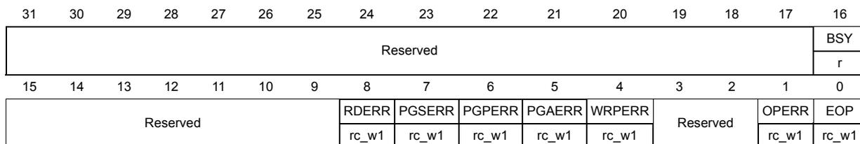
3.9.5 Flash status register (FLASH_SR) for STM32F405xx/07xx and STM32F415xx/17xx
The Flash status register gives information on ongoing program and erase operations.
Address offset: 0x0C
Reset value: 0x0000 0000
Access: no wait state, word, half-word and byte access
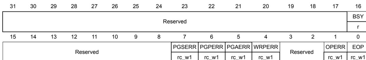
| 31 | 30 | 29 | 28 | 27 | 26 | 25 | 24 | 23 | 22 | 21 | 20 | 19 | 18 | 17 | 16 |
| Reserved | BSY r | ||||||||||||||
| 15 | 14 | 13 | 12 | 11 | 10 | 9 | 8 | 7 | 6 | 5 | 4 | 3 | 2 | 1 | 0 |
| Reserved | PGSERR rc_w1 | PGPERR rc_w1 | PGAERR rc_w1 | WRPERR rc_w1 | Reserved | OPERR rc_w1 | EOP rc_w1 | ||||||||
Bits 31:17 Reserved, must be kept cleared.
Bit 16 BSY : Busy
This bit indicates that a flash memory operation is in progress. It is set at the beginning of a flash memory operation and cleared when the operation finishes or an error occurs.
0: no flash memory operation ongoing
1: Flash memory operation ongoing
Bits 15:8 Reserved, must be kept cleared.
Bit 7 PGSERR : Programming sequence error
Set by hardware when a write access to the flash memory is performed by the code while the control register has not been correctly configured.
Cleared by writing 1.
Bit 6 PGPERR : Programming parallelism error
Set by hardware when the size of the access (byte, half-word, word, double word) during the program sequence does not correspond to the parallelism configuration PSIZE (x8, x16, x32, x64).
Cleared by writing 1.
Bit 5 PGAERR : Programming alignment error
Set by hardware when the data to program cannot be contained in the same 128-bit flash memory row.
Cleared by writing 1.
Bit 4 WRPERR : Write protection error
Set by hardware when an address to be erased/programmed belongs to a write-protected part of the flash memory.
Cleared by writing 1.
Bits 3:2 Reserved, must be kept cleared.
Bit 1 OPERR : Operation error
Set by hardware when a flash operation (programming / erase /read) request is detected and can not be run because of parallelism, alignment, or write protection error. This bit is set only if error interrupts are enabled (ERRIE = 1).
Bit 0 EOP : End of operation
Set by hardware when one or more flash memory operations (program/erase) has/have completed successfully. It is set only if the end of operation interrupts are enabled (EOPIE = 1). Cleared by writing a 1.
3.9.6 Flash status register (FLASH_SR) for STM32F42xxx and STM32F43xxx
The Flash status register gives information on ongoing program and erase operations.
Address offset: 0x0C
Reset value: 0x0000 0000
Access: no wait state, word, half-word and byte access
| 31 | 30 | 29 | 28 | 27 | 26 | 25 | 24 | 23 | 22 | 21 | 20 | 19 | 18 | 17 | 16 | |
| Reserved | BSY | |||||||||||||||
| r | ||||||||||||||||
| 15 | 14 | 13 | 12 | 11 | 10 | 9 | 8 | 7 | 6 | 5 | 4 | 3 | 2 | 1 | 0 | |
| Reserved | RDERR | PGSERR | PGPERR | PGAERR | WRPERR | Reserved | OPERR | EOP | ||||||||
| rc_w1 | rc_w1 | rc_w1 | rc_w1 | rc_w1 | rc_w1 | rc_w1 | ||||||||||
Bits 31:17 Reserved, must be kept cleared.
Bit 16 BSY : Busy
This bit indicates that a flash memory operation is in progress to/from one bank. It is set at the beginning of a flash memory operation and cleared when the operation finishes or an error occurs.
0: no flash memory operation ongoing
1: Flash memory operation ongoing
Bits 15:9 Reserved, must be kept cleared.
Bit 8 RDERR : Proprietary readout protection (PCROP) error
Set by hardware when a read access through the D-bus is performed to an address belonging to a proprietary readout protected Flash sector.
Cleared by writing 1.
Bit 7 PGSERR : Programming sequence error
Set by hardware when a write access to the flash memory is performed by the code while the control register has not been correctly configured.
Cleared by writing 1.
Bit 6 PGPERR : Programming parallelism error
Set by hardware when the size of the access (byte, half-word, word, double word) during the program sequence does not correspond to the parallelism configuration PSIZE (x8, x16, x32, x64).
Cleared by writing 1.
Bit 5 PGAERR : Programming alignment error
Set by hardware when the data to program cannot be contained in the same 128-bit flash memory row.
Cleared by writing 1.
Bit 4 WRPERR : Write protection error
Set by hardware when an address to be erased/programmed belongs to a write-protected part of the flash memory.
Cleared by writing 1.
Bits 3:2 Reserved, must be kept cleared.
Bit 1 OPERR : Operation error
Set by hardware when a flash operation (programming/erase/read) request is detected and can not be run because of parallelism, alignment, write or read (PCROP) protection error. This bit is set only if error interrupts are enabled (ERRIE = 1).
Bit 0 EOP : End of operation
Set by hardware when one or more flash memory operations (program/erase) has/have completed successfully. It is set only if the end of operation interrupts are enabled (EOPIE = 1).
Cleared by writing a 1.
3.9.7 Flash control register (FLASH_CR) for STM32F405xx/07xx and STM32F415xx/17xx
The Flash control register is used to configure and start flash memory operations.
Address offset: 0x10
Reset value: 0x8000 0000
Access: no wait state when no flash memory operation is ongoing, word, half-word and byte access.
| 31 | 30 | 29 | 28 | 27 | 26 | 25 | 24 | 23 | 22 | 21 | 20 | 19 | 18 | 17 | 16 |
|---|---|---|---|---|---|---|---|---|---|---|---|---|---|---|---|
| LOCK | Reserved | ERRIE | EOPIE | Reserved | STRT | ||||||||||
| rs | rw | rw | rs | ||||||||||||
| 15 | 14 | 13 | 12 | 11 | 10 | 9 | 8 | 7 | 6 | 5 | 4 | 3 | 2 | 1 | 0 |
|---|---|---|---|---|---|---|---|---|---|---|---|---|---|---|---|
| Reserved | PSIZE[1:0] | Res. | SNB[3:0] | MER | SER | PG | |||||||||
| rw | rw | rw | rw | rw | rw | rw | rw | rw | |||||||
Bit 31 LOCK : Lock
Write to 1 only. When it is set, this bit indicates that the FLASH_CR register is locked. It is cleared by hardware after detecting the unlock sequence.
In the event of an unsuccessful unlock operation, this bit remains set until the next reset.
Bits 30:26 Reserved, must be kept cleared.
Bit 25 ERRIE : Error interrupt enable
This bit enables the interrupt generation when the OPERR bit in the FLASH_SR register is set to 1.
0: Error interrupt generation disabled
1: Error interrupt generation enabled
Bit 24 EOPIE : End of operation interrupt enable
This bit enables the interrupt generation when the EOP bit in the FLASH_SR register goes to 1.
0: Interrupt generation disabled
1: Interrupt generation enabled
Bits 23:17 Reserved, must be kept cleared.
Bit 16 STRT : Start
This bit triggers an erase operation when set. It is set only by software and cleared when the BSY bit is cleared.
Bits 15:10 Reserved, must be kept cleared.
Bits 9:8 PSIZE[1:0] : Program size
These bits select the program parallelism.
00 program x8
01 program x16
10 program x32
11 program x64
Bit 7 Reserved, must be kept cleared.
Bits 6:3 SNB[3:0] : Sector number
These bits select the sector to erase.
0000 sector 0
0001 sector 1
...
1011 sector 11
Others not allowed
Bit 2 MER : Mass Erase
Erase activated for all user sectors.
Bit 1 SER : Sector Erase
Sector Erase activated.
Bit 0 PG : Programming
Flash programming activated.
3.9.8 Flash control register (FLASH_CR) for STM32F42xxx and STM32F43xxx
The Flash control register is used to configure and start flash memory operations.
Address offset: 0x10
Reset value: 0x8000 0000
Access: no wait state when no flash memory operation is ongoing, word, half-word and byte access.
| 31 | 30 | 29 | 28 | 27 | 26 | 25 | 24 | 23 | 22 | 21 | 20 | 19 | 18 | 17 | 16 |
|---|---|---|---|---|---|---|---|---|---|---|---|---|---|---|---|
| LOCK | Reserved | ERRIE | EOPIE | Reserved | STRT | ||||||||||
| rs | rw | rw | rs | ||||||||||||
| 15 | 14 | 13 | 12 | 11 | 10 | 9 | 8 | 7 | 6 | 5 | 4 | 3 | 2 | 1 | 0 |
| MER1 | Reserved | PSIZE[1:0] | SNB[4:0] | MER | SER | PG | |||||||||
| rw | rw | rw | rw | rw | rw | rw | rw | rw | rw | rw | |||||
Bit 31 LOCK: Lock
Write to 1 only. When it is set, this bit indicates that the FLASH_CR register is locked. It is cleared by hardware after detecting the unlock sequence.
In the event of an unsuccessful unlock operation, this bit remains set until the next reset.
Bits 30:26 Reserved, must be kept cleared.
Bit 25 ERRIE: Error interrupt enable
This bit enables the interrupt generation when the OPERR bit in the FLASH_SR register is set to 1.
0: Error interrupt generation disabled
1: Error interrupt generation enabled
Bit 24 EOPIE: End of operation interrupt enable
This bit enables the interrupt generation when the EOP bit in the FLASH_SR register goes to 1.
0: Interrupt generation disabled
1: Interrupt generation enabled
Bits 23:17 Reserved, must be kept cleared.
Bit 16 STRT: Start
This bit triggers an erase operation when set. It is set only by software and cleared when the BSY bit is cleared.
Bit 15 MER1: Mass Erase of bank 2 sectors
Erase activated for bank 2 user sectors 12 to 23.
Bits 14:10 Reserved, must be kept cleared.
Bits 9:8 PSIZE[1:0]: Program size
These bits select the program parallelism.
00 program x8
01 program x16
10 program x32
11 program x64
Bits 7:3 SNB[3:0] : Sector number
These bits select the sector to erase.
- 0000: sector 0
- 0001: sector 1
- ...
- 01011: sector 11
- 01100: not allowed
- 01101: not allowed
- 01110: not allowed
- 01111: not allowed
- 10000: sector 12
- 10001: sector 13
- ...
- 11011 sector 23
- 11100: not allowed
- 11101: not allowed
- 11110: not allowed
- 11111: not allowed
Bit 2 MER : Mass Erase of bank 1 sectors
Erase activated of bank 1 sectors.
Bit 1 SER : Sector Erase
Sector Erase activated.
Bit 0 PG : Programming
Flash programming activated.
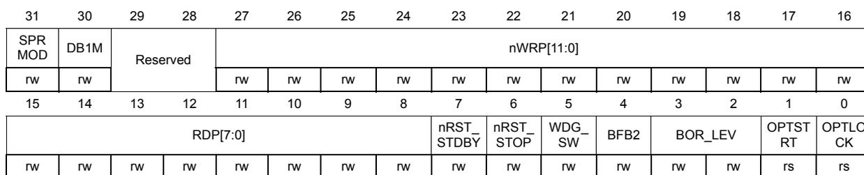
3.9.9 Flash option control register (FLASH_OPTCR) for STM32F405xx/07xx and STM32F415xx/17xx
The FLASH_OPTCR register is used to modify the user option bytes.
Address offset: 0x14
Reset value: 0x0FFF AAED. The option bits are loaded with values from flash memory at reset release.
Access: no wait state when no flash memory operation is ongoing, word, half-word and byte access.
| 31 | 30 | 29 | 28 | 27 | 26 | 25 | 24 | 23 | 22 | 21 | 20 | 19 | 18 | 17 | 16 |
|---|---|---|---|---|---|---|---|---|---|---|---|---|---|---|---|
| Reserved | nWRP[11:0] | ||||||||||||||
| rw | rw | rw | rw | rw | rw | rw | rw | rw | rw | rw | rw | ||||
| 15 | 14 | 13 | 12 | 11 | 10 | 9 | 8 | 7 | 6 | 5 | 4 | 3 | 2 | 1 | 0 |
| RDP[7:0] | nRST_ STDBY | nRST_ STOP | WDG_ SW | Reserve d | BOR_LEV | OPTST RT | OPTLO CK | ||||||||
| rw | rw | rw | rw | rw | rw | rw | rw | rw | rw | rw | rw | rw | rs | rs | |
Bits 31:28 Reserved, must be kept cleared.
Bits 27:16 nWRP[11:0] : Not write protect
These bits contain the value of the write-protection option bytes after reset. They can be written to program a new write protect value into flash memory.
- 0: Write protection active on selected sector
- 1: Write protection inactive on selected sector
Bits 15:8 RDP[7:0] : Read protect
These bits contain the value of the read-protection option level after reset. They can be written to program a new read protection value into flash memory.
- 0xAA: Level 0, read protection not active
- 0xCC: Level 2, chip read protection active
- Others: Level 1, read protection of memories active
Bits 7:5 USER[2:0] : User option bytes
These bits contain the value of the user option byte after reset. They can be written to program a new user option byte value into flash memory.
- Bit 7: nRST_STDBY
- Bit 6: nRST_STOP
- Bit 5: WDG_SW
Note: When changing the WDG mode from hardware to software or from software to hardware, a system reset is required to make the change effective.
Bit 4 Reserved, must be kept cleared. Always read as “0”.
Bits 3:2 BOR_LEV[1:0] : BOR reset Level
These bits contain the supply level threshold that activates/releases the reset. They can be written to program a new BOR level. By default, BOR is off. When the supply voltage ( \( V_{DD} \) ) drops below the selected BOR level, a device reset is generated.
- 00: BOR Level 3 (VBOR3), brownout threshold level 3
- 01: BOR Level 2 (VBOR2), brownout threshold level 2
- 10: BOR Level 1 (VBOR1), brownout threshold level 1
- 11: BOR off, POR/PDR reset threshold level is applied
Note: For full details about BOR characteristics, refer to the “Electrical characteristics” section in the device datasheet.
Bit 1 OPTSTRT : Option start
This bit triggers a user option operation when set. It is set only by software and cleared when the BSY bit is cleared.
Bit 0 OPTLOCK : Option lock
Write to 1 only. When this bit is set, it indicates that the FLASH_OPTCR register is locked. This bit is cleared by hardware after detecting the unlock sequence.
In the event of an unsuccessful unlock operation, this bit remains set until the next reset.
3.9.10 Flash option control register (FLASH_OPTCR)
for STM32F42xxx and STM32F43xxx
The FLASH_OPTCR register is used to modify the user option bytes.
Address offset: 0x14
Reset value: 0x0FFF AAED. The option bits are loaded with values from flash memory at reset release.
Access: no wait state when no flash memory operation is ongoing, word, half-word and byte access.
| 31 | 30 | 29 | 28 | 27 | 26 | 25 | 24 | 23 | 22 | 21 | 20 | 19 | 18 | 17 | 16 |
| SPR MOD | DB1M | Reserved | nWRP[11:0] | ||||||||||||
| rw | rw | rw | rw | rw | rw | rw | rw | rw | rw | rw | rw | rw | rw | ||
| 15 | 14 | 13 | 12 | 11 | 10 | 9 | 8 | 7 | 6 | 5 | 4 | 3 | 2 | 1 | 0 |
| RDP[7:0] | nRST_ STDBY | nRST_ STOP | WDG_ SW | BFB2 | BOR_LEV | OPTST RT | OPTLO CK | ||||||||
| rw | rw | rw | rw | rw | rw | rw | rw | rw | rw | rw | rw | rw | rw | rs | rs |
Bit 31 SPRMOD : Selection of protection mode for nWPRi bits
- 0: PCROP disabled. nWPRi bits used for Write protection on sector i.
- 1: PCROP enabled. nWPRi bits used for PCROP protection on sector i
Bit 30 DB1M : Dual-bank on 1 Mbyte flash memory devices
- 0: 1 Mbyte single bank flash memory (contiguous addresses in bank1)
- 1: 1 Mbyte dual bank flash memory. The flash memory is organized as two banks of 512 Kbytes each (see Table 7: 1 Mbyte flash memory single bank vs dual bank organization (STM32F42xxx and STM32F43xxx) and Table 9: 1 Mbyte dual bank flash memory organization (STM32F42xxx and STM32F43xxx) ). To perform an erase operation, the right sector must be programmed (see Table 7 for information on the sector numbering scheme).
Note: If DB1M is set and an erase operation is performed on Bank 2 while the default sector number is selected (as an example, sector 8 is configured instead of sector 12), the erase operation on Bank 2 sector is not performed.
Bits 29:28 Reserved, must be kept cleared.
Bits 27:16 nWRP[11:0] : Not write protect
These bits contain the value of the write-protection and read-protection (PCROP) option bytes for sectors 0 to 11 after reset. They can be written to program a new write-protect or PCROP value into flash memory.
- If SPRMOD is reset:
- 0: Write protection active on sector i
- 1: Write protection not active on sector i
- If SPRMOD is set:
- 0: PCROP protection not active on sector i
- 1: PCROP protection active on sector i
Bits 15:8 RDP[7:0] : Read protect
These bits contain the value of the read-protection option level after reset. They can be written to program a new read protection value into flash memory.
- 0xAA: Level 0, read protection not active
- 0xCC: Level 2, chip read protection active
- Others: Level 1, read protection of memories active
These bits contain the value of the user option byte after reset. They can be written to program a new user option byte value into flash memory.
- Bit 7: nRST_STDBY
- Bit 6: nRST_STOP
- Bit 5: WDG_SW
Note: When changing the WDG mode from hardware to software or from software to hardware, a system reset is required to make the change effective.
Bit 4 BFB2: Dual-bank Boot option byte- 0: Dual-bank boot disabled. Boot can be performed either from flash memory bank 1 or from system memory depending on boot pin state (default)
- 1: Dual-bank boot enabled. Boot is always performed from system memory.
Note: For STM32F42xx and STM32F43xx 1MB part numbers, this option bit must be kept cleared when DB1M=0.
Bits 3:2 BOR_LEV: BOR reset LevelThese bits contain the supply level threshold that activates/releases the reset. They can be written to program a new BOR level. By default, BOR is off. When the supply voltage ( \( V_{DD} \) ) drops below the selected BOR level, a device reset is generated.
- 00: BOR Level 3 (VBOR3), brownout threshold level 3
- 01: BOR Level 2 (VBOR2), brownout threshold level 2
- 10: BOR Level 1 (VBOR1), brownout threshold level 1
- 11: BOR off, POR/PDR reset threshold level is applied
Note: For full details on BOR characteristics, refer to the “Electrical characteristics” section of the product datasheet.
Bit 1 OPTSTRT: Option startThis bit triggers a user option operation when set. It is set only by software and cleared when the BSY bit is cleared.
Bit 0 OPTLOCK: Option lockWrite to 1 only. When this bit is set, it indicates that the FLASH_OPTCR register is locked. This bit is cleared by hardware after detecting the unlock sequence.
In the event of an unsuccessful unlock operation, this bit remains set until the next reset.
3.9.11 Flash option control register (FLASH_OPTCR1) for STM32F42xxx and STM32F43xxx
This register is available only on STM32F42xxx and STM32F43xxx.
The FLASH_OPTCR1 register is used to modify the user option bytes for bank 2.
Address offset: 0x18
Reset value: 0x0FFF 0000. The option bits are loaded with values from flash memory at reset release.
Access: no wait state when no flash memory operation is ongoing, word, half-word and byte access.
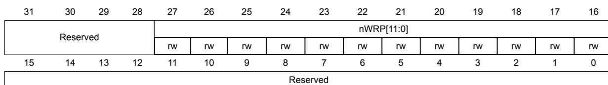
| 31 | 30 | 29 | 28 | 27 | 26 | 25 | 24 | 23 | 22 | 21 | 20 | 19 | 18 | 17 | 16 |
| Reserved | nWRP[11:0] | ||||||||||||||
| rw | rw | rw | rw | rw | rw | rw | rw | rw | rw | rw | rw | ||||
| 15 | 14 | 13 | 12 | 11 | 10 | 9 | 8 | 7 | 6 | 5 | 4 | 3 | 2 | 1 | 0 |
| Reserved | |||||||||||||||
Bits 31:28 Reserved, must be kept cleared.
Bits 27:16 nWRP[11:0] : Not write protect
These bits contain the value of the write-protection and read-protection (PCROP) option bytes for sectors 0 to 11 after reset. They can be written to program a new write-protect or PCROP value into flash memory.
If SPRMOD is reset (default value):
- 0: Write protection active on sector i.
- 1: Write protection not active on sector i.
If SPRMOD is set:
- 0: PCROP protection not active on sector i.
- 1: PCROP protection active on sector i.
Bits 15:0 Reserved, must be kept cleared.
3.9.12 Flash interface register map
Table 20. Flash register map and reset values(STM32F405xx/07xx and STM32F415xx/17xx)
| Offset | Register | 31 | 30 | 29 | 28 | 27 | 26 | 25 | 24 | 23 | 22 | 21 | 20 | 19 | 18 | 17 | 16 | 15 | 14 | 13 | 12 | 11 | 10 | 9 | 8 | 7 | 6 | 5 | 4 | 3 | 2 | 1 | 0 |
|---|---|---|---|---|---|---|---|---|---|---|---|---|---|---|---|---|---|---|---|---|---|---|---|---|---|---|---|---|---|---|---|---|---|
| 0x00 | FLASH_ACR | Reserved | DCRST | ICRST | DCEN | ICEN | PRFTEN | Reserved | LATENCY [2:0] | ||||||||||||||||||||||||
| Reset value | 0 | 0 | 0 | 0 | 0 | 0 | 0 | 0 | |||||||||||||||||||||||||
| 0x04 | FLASH_KEYR | KEY[31:16] | KEY[15:0] | ||||||||||||||||||||||||||||||
| Reset value | 0 | 0 | 0 | 0 | 0 | 0 | 0 | 0 | 0 | 0 | 0 | 0 | 0 | 0 | 0 | 0 | 0 | 0 | 0 | 0 | 0 | 0 | 0 | 0 | 0 | 0 | 0 | 0 | 0 | 0 | 0 | 0 | |
| 0x08 | FLASH_OPTKEYR | OPTKEYR[31:16] | OPTKEYR[15:0] | ||||||||||||||||||||||||||||||
| Reset value | 0 | 0 | 0 | 0 | 0 | 0 | 0 | 0 | 0 | 0 | 0 | 0 | 0 | 0 | 0 | 0 | 0 | 0 | 0 | 0 | 0 | 0 | 0 | 0 | 0 | 0 | 0 | 0 | 0 | 0 | 0 | 0 | |
| 0x0C | FLASH_SR | Reserved | BSY | Reserved | PGSERR | PGPERR | PGAERR | WRPERR | Reserved | OPERR | EOP | ||||||||||||||||||||||
| Reset value | 0 | 0 | 0 | 0 | 0 | 0 | 0 | ||||||||||||||||||||||||||
| 0x10 | FLASH_CR | LOCK | Reserved | EOPIE | Reserved | STRT | Reserved | PSIZE[1:0] | Reserved | SNB[3:0] | MER | SER | PG | ||||||||||||||||||||
| Reset value | 1 | 0 | 0 | 0 | 0 | 0 | 0 | 0 | 0 | 0 | 0 | ||||||||||||||||||||||
| 0x14 | FLASH_OPTCR | Reserved | nWRP[11:0] | RDP[7:0] | nRST_STDBY | nRST_STOP | WDG_SW | Reserved | BOR_LEV[1:0] | OPTSTRT | OPTLOCK | ||||||||||||||||||||||
| Reset value | 1 | 1 | 1 | 1 | 1 | 1 | 1 | 1 | 1 | 1 | 1 | 1 | 1 | 0 | 1 | 0 | 1 | 0 | 1 | 0 | 1 | 1 | 1 | 1 | 1 | 0 | 1 | ||||||
| Offset | Register | 31 | 30 | 29 | 28 | 27 | 26 | 25 | 24 | 23 | 22 | 21 | 20 | 19 | 18 | 17 | 16 | 15 | 14 | 13 | 12 | 11 | 10 | 9 | 8 | 7 | 6 | 5 | 4 | 3 | 2 | 1 | 0 |
|---|---|---|---|---|---|---|---|---|---|---|---|---|---|---|---|---|---|---|---|---|---|---|---|---|---|---|---|---|---|---|---|---|---|
| 0x00 | FLASH_ACR | Reserved | DCRST | ICRST | DCEN | ICEN | PRFTEN | Reserved | LATENCY[3:0] | ||||||||||||||||||||||||
| Reset value | 0 | 0 | 0 | 0 | 0 | 0 | 0 | 0 | 0 | ||||||||||||||||||||||||
| 0x04 | FLASH_KEYR | KEY[31:16] | KEY[15:0] | ||||||||||||||||||||||||||||||
| Reset value | 0 | 0 | 0 | 0 | 0 | 0 | 0 | 0 | 0 | 0 | 0 | 0 | 0 | 0 | 0 | 0 | 0 | 0 | 0 | 0 | 0 | 0 | 0 | 0 | 0 | 0 | 0 | 0 | 0 | 0 | 0 | 0 | |
| 0x08 | FLASH_OPTKEYR | OPTKEYR[31:16] | OPTKEYR[15:0] | ||||||||||||||||||||||||||||||
| Reset value | 0 | 0 | 0 | 0 | 0 | 0 | 0 | 0 | 0 | 0 | 0 | 0 | 0 | 0 | 0 | 0 | 0 | 0 | 0 | 0 | 0 | 0 | 0 | 0 | 0 | 0 | 0 | 0 | 0 | 0 | 0 | 0 | |
| 0x0C | FLASH_SR | Reserved | BSY | Reserved | RDERR | PGSERR | PGPERR | PGAERR | WRPERR | Reserved | OPERR | EOP | |||||||||||||||||||||
| Reset value | 0 | 0 | 0 | 0 | 0 | 0 | 0 | 0 | |||||||||||||||||||||||||
| Offset | Register | 31 | 30 | 29 | 28 | 27 | 26 | 25 | 24 | 23 | 22 | 21 | 20 | 19 | 18 | 17 | 16 | 15 | 14 | 13 | 12 | 11 | 10 | 9 | 8 | 7 | 6 | 5 | 4 | 3 | 2 | 1 | 0 |
|---|---|---|---|---|---|---|---|---|---|---|---|---|---|---|---|---|---|---|---|---|---|---|---|---|---|---|---|---|---|---|---|---|---|
| 0x10 | FLASH_CR | LOCK | Reserved | EOPIE | Reserved | STRT | MER1 | Reserved | PSIZE[1:0] | SNB[4:0] | MER | SER | PG | ||||||||||||||||||||
| Reset value | 1 | 0 | 0 | 0 | 0 | 0 | 0 | 0 | 0 | 0 | 0 | 0 | 0 | 0 | |||||||||||||||||||
| 0x14 | FLASH_OPTCR | SPRMOD | DB1M | Reserved | nWRP[11:0] | RDP[7:0] | nRST_STDBY | nRST_STOP | WDG_SW | BFB2 | BOR_LEV[1:0] | OPTSTRT | OPTLOCK | ||||||||||||||||||||
| Reset value | 0 | 0 | 1 | 1 | 1 | 1 | 1 | 1 | 1 | 1 | 1 | 1 | 1 | 1 | 1 | 0 | 1 | 0 | 1 | 0 | 1 | 0 | 1 | 1 | 1 | 1 | 0 | 1 | 1 | 0 | 1 | ||
| 0x18 | FLASH_OPTCR1 | Reserved | nWRP[11:0] | Reserved | |||||||||||||||||||||||||||||
| Reset value | 1 | 1 | 1 | 1 | 1 | 1 | 1 | 1 | 1 | 1 | 1 | 1 | |||||||||||||||||||||