24. High-definition multimedia interface-consumer electronics control controller (HDMI™-CEC)
Low-density value line devices are STM32F100xx microcontrollers where the flash memory density ranges between 16 and 32 Kbytes.
Medium-density value line devices are STM32F100xx microcontrollers where the flash memory density ranges between 64 and 128 Kbytes.
High-density value line devices are STM32F100xC, STM32F100xD and STM32F100xE microcontrollers where the flash memory density ranges between 256 and 512 Kbytes.
This section applies to all STM32F100xx devices, unless otherwise specified.
24.1 Introduction
Consumer electronics control (CEC) is the appendix supplement 1 to the HDMI (high-definition multimedia interface) standard.
It is a protocol that provides high-level control functions between all of the various audiovisual products in an environment. It is specified to operate at low speeds with minimum processing and memory overhead.
The HDMI-CEC controller provides a hardware support of this protocol.
24.2 HDMI-CEC main features
- • Supports HDMI-CEC v1.3a
- • Supports the whole set of features offered with CEC (devices may use all or only some of these features, depending on functionality):
- – One touch play - a device may be played and become the active source by pressing a single button.
- – System standby - enables devices to be set on standby by pressing a single button.
- – Preset transfer - the presets of a device can be auto-configured to match those of the TV.
- – One touch record - Used to make recordings by pressing a single button.
- – Timer programming - any device can program a timer recording on a recording device.
- – System information - allows devices to auto-configure their language and country settings.
- – Deck control - allows a device to control and interrogate a playback device.
- – Tuner control - allows a device to control the tuner of another device.
- – Vendor specific commands - allows vendor-defined commands to be used.
- – OSD display - allows a device to display text using the on-screen display of the TV.
- – Device menu control - allows a device to control the menu of another device.
- – Routing control - Enables control of CEC switches for the streaming of a new source device.
- – Remote control pass through - allows remote control commands to be passed along to other devices.
- – Device OSD name transfer - devices may request the preferred OSD name of other devices within the system.
Note: If you need the power-off state, you have to use an external component/transceiver. For more details refer to AN3127: “CEC networking using STM32F100xx value line microcontrollers”.
24.3 HDMI-CEC bus topology
24.3.1 HDMI-CEC pin
The CEC bus consists of a single bidirectional line that is used to transfer data in and out of the device. It is connected to a +3.3 V supply voltage via a 27 kΩ pull-up resistor. The output stage of the device must have an open-drain or open-collector to allow a wired-AND connection.
The HDMI-CEC controller manages the CEC bidirectional line as an alternate function of a standard GPIO, assuming that it is configured as alternate function open drain. The 27 kΩ pull-up resistor must be added externally to the STM32F100xx.
Table 135. HDMI pin
| Name | Signal type | Remarks |
|---|---|---|
| CEC | Bidirectional | Two states: 1 = high impedance 0 = low impedance A 27 k \( \Omega \) pull-up resistor must be added externally. |
Figure 268. CEC line connection
1. When configured as output open-drain alternate function, the Schmitt trigger is still activated.
- Note:
- 1 If you do not need the power-off state, you may simply connect the STM32F100xx microcontroller to the CEC line.
- 2 If the power-off state is needed in the application, the external pull-up circuit has to be disconnected from the CEC line when the device is off. For example, this can be implemented by connecting an isolating diode between the CEC line and the external pull-up circuit, such that the diode is reverse-biased in the off state with an external device pulling up the CEC line. A bidirectional isolation buffer is also needed to comply with the HDMI 1.3a specification. For more details refer to AN3127: “CEC networking using STM32F100xx value line microcontrollers”.
24.3.2 Message description
All transactions on the CEC line consist of an initiator and one or more followers. The initiator is responsible for sending the message structure and the data. The follower is the recipient of any data and is responsible for setting any acknowledgement bits.
A message is conveyed in a single frame that consists of a start bit followed by a header block and, optionally, an opcode and a variable number of operand blocks.
All these blocks are made of a 8-bit payload (most significant bit transmitted first) followed by an end-of-message (EOM) bit and an acknowledge (ACK) bit.
The EOM bit is set in the last block of a message and kept cleared in all others. In the event that a message contains additional blocks after an EOM is indicated, those additional blocks should be ignored. The EOM bit may be set in the header block to “ping” other devices, to ascertain if they are active.
The acknowledge bit is always set to high impedance by the initiator so that it can be driven low either by the follower that has read its own address in the header or by the follower that needs to reject a broadcast message.
The header consists of the source logical address field, and the destination logical address field. Note that the special address 0xF is used for broadcast messages.
Figure 269. Message structure
The diagram shows a message structure starting with 'high impedance', followed by a 'Start bit', 'Header', 'Opcode', and then 'Operand' fields. A bracket above the operand fields indicates '0 to 14 operands'. The message ends with 'high impedance'. The identifier 'ai17315' is in the bottom right corner.
Figure 270. Blocks
The diagram shows two block types: 'Header block' containing INITIATOR[3:0], DESTINATION[3:0], EOM, and ACK; and 'Opcode/operand block' containing DATA[7:0], EOM, and ACK. The identifier 'ai17316' is in the bottom right corner.
24.3.3 Bit timing
The format of the start bit is unique and identifies the start of a message. It should be validated by its low duration and its total duration.
All remaining data bits in the message, after the start bit, have consistent timing. The high-to-low transition at the end of the data bit is the start of the next data bit except for the final bit where the CEC line remains high.
Figure 271. Bit timings
The diagram shows timing for 'Start bit' and 'Data bit'. For the 'Start bit', the total duration is 4.5 ms ± 0.2 ms and the low duration is 3.7 ms ± 0.2 ms. For 'Data bit INITIATOR logical 0', the total duration is 2.4 ms ± 0.35 ms and the low duration is 1.5 ms ± 0.2 ms. For 'Data bit INITIATOR logical 1', the total duration is 2.4 ms ± 0.35 ms and the high duration is 0.6 ms ± 0.2 ms. The identifier 'ai17317' is in the bottom right corner.
CEC Figure 272 shows an example bit with both initiator and follower where the follower may assert the bit to logical 0 to acknowledge a data block. The initiator outputs a logical 1, thus allowing the follower to change the CEC state by pulling the control line low for the duration of the safe sample period.
Figure 272. Follower acknowledge (ACK)
24.4 Arbitration
24.4.1 Signal free time (SFT)
All devices that are to transmit or retransmit a message onto the CEC line have to ensure that the line has been inactive for a number of bit periods. This signal free time (SFT) is defined as the time from the start of the final bit of the previous frame, and depends on the initiating device and the current status as shown in the table below.
Figure 273. Signal free time

Table 136. Signal free time definition
| Condition | Signal free time (in nominal data bit periods) |
|---|---|
| Present initiator has to send another frame immediately after the one it just sent | ≥ 7 |
| New initiator has to send a frame | ≥ 5 |
| Previous attempt to send frame unsuccessful | ≥ 3 |
24.4.2 Header arbitration
Figure 274. Arbitration phase
![Timing diagram for the Arbitration phase showing the sequence of bits: Start bit, INITIATOR[3:0], DESTINATION[3:0], EOM, and ACK. The arbitration phase begins with the leading edge of the start bit. Reference ai17319.](/RM0041-STM32F100/d422ed5d28b77f4019be97b2c4b4cdfa_img.jpg)
Since only one initiator is allowed at any one time, the header arbitration mechanism is provided to avoid conflict when more than one initiator has to send a frame within the same allowed SFT slot. Header arbitration begins with the leading edge of the start bit and
continues until the end of the initiator address bits within the header block. During the header transmission period the initiator monitors the CEC line and if it detects a low impedance while it is in the high impedance state, then it assumes that it has lost the arbitration to a second initiator. Note that this process gives priority to the logical address with the highest number of leading zeros and, ultimately, the TV (INITIATOR=0x0).
24.5 Error handling
24.5.1 BTE, BPE and Error bit generation
A received data bit (excluding the start bit) is considered invalid if:
- • the period between the falling and the rising edge exceeds the tolerance margins as defined by the HDMI-CEC Specification Rev1.3a, Sect5.5.2, Figure4. In this case a Bit Timing Error (BTE) is issued.
- • the period between falling edges exceeds the tolerance margins as defined by the HDMI-CEC Specification, Rev1.3a Sect5.5.2, Figure4. In this case a Bit Period Error (BPE) is issued.
- • When both BPE and BTE are detected, BTE only is signalled.
If a BTE or BPE receive error is detected, the CEC peripheral is expected to notify such events to the other followers, and primarily to the initiator, by generating an Error bit: a low period on the CEC line of 1.4 to 1.6 times the nominal data bit period, that is, 3.6 ms nominally.
Figure 275. Error bit timing
The diagram illustrates the timing of an error bit. It shows a signal line that starts in a high impedance state, drops to a low impedance state, and then returns to a high impedance state. The duration of the low impedance state is indicated by a horizontal double-headed arrow and labeled as 3.6 ms ±0.24 ms. The signal levels are labeled 'high impedance' and 'low impedance'. The diagram is labeled 'Error bit' and 'ai17320'.
24.5.2 Message error
A message is considered lost and therefore may be retransmitted under the following conditions:
- • a message is not acknowledged in a directly addressed message
- • a message is negatively acknowledged in a broadcast message
- • a low impedance is detected on the CEC line when not expected (line error)
Retransmission should be attempted at least once and up to five times.
24.6 Device addressing
Apart from the physical address (refer to the HDMI-CEC specification for more details on physical address discovery), each device appearing on the control signal line (CEC Line) has a unique logical address. This address defines a device type as well as being a unique identifier. This address is 0 for a TV set with physical address 0b0000 and 14 or even 15 otherwise. It is defined in the CEC_OAR register and in the upper nibble of the first byte of
the transmitted message. All CEC devices therefore have both a physical and a logical address, whereas non-CEC devices only have a physical address.
Once their physical and logical addresses are known, each CEC device transmits them to all other devices, thus allowing any device to create a map of the network.
24.7 HDMI-CEC functional description
24.7.1 Block diagram
The HDMI-CEC controller handles complete messages but requires the CPU to provide or unload the data bytes one by one.
Figure 276 shows the CEC controller block diagram.
Figure 276. HDMI-CEC block diagram
- 1. The timing checker block verifies the received bit timings, while the timing generator controls the transmitted bit timings.
24.7.2 Prescaler
The prescaler defines the time quantum for the timing checker and timing generator blocks. Additionally, it provides a time quantum reference for complying with the required signal free time (SFT). A 14-bit counter is used to provide the necessary 50 microsecond time base, allowing high APB clocks frequency.
The counter is reset at the beginning of every bit for the timing checker block to operate with the maximum precision.
Prescaler formula for nominal bit timings is:
24.7.3 Rx digital filter
CEC robustness in the face of CEC line perturbation is guaranteed by two noise rejection mechanisms:
- • high-frequency spikes are removed by a 2/3 majority voter applied on the Rx line sampled at the system clock rate
- • line rebounds are filtered until the next 50 µs time window entirely following any CEC line transition
24.7.4 Rx bit timing
The CEC operates at a 50 µs time quantum since the bits timings are expressed with this precision. It extracts valid bits from the CEC line and signals line errors when detected.
On a valid Rx falling edge, the value of the time counter is captured and reset. This value indicates the total bit duration and is named m . If the captured value is outside the valid range (see table below), a bit period error is detected and signalled by pulling the line low for 3.6 ms (typical).
On a valid Rx rising edge, the value of the time counter is captured and compared to valid windows. This value indicates the low bit duration and is named n . If the low bit duration (the timing between the falling and rising edges) is outside the valid range, a bit timing error is detected and signalled by pulling the line low for 3.6 ms (typical) unless the device was programmed not to report this type of violations.
Note: If a line error occurs while a start bit is expected, the whole message is ignored and no error is reported.
In the absence of a rising edge, the time counter counts up to 25.6 ms. Retransmission is allowed when its value is above 9.6 ms. A new initiator may transmit when the time counter is above 14.4 ms. The same initiator must however wait until the counter reaches 19.2 ms.
Note: Due to Rx synchronization and digital filtering, all CEC timings are calculated with a precision tolerance of 4 APB clock cycles.
Figure 277. Bit timing
Table 137. Bit status depending on the low bit duration (LBD)
| Low bit duration (LBD) (ms) | Bit | |
|---|---|---|
| Standard mode (BTEM = 0) (1) | Bit timing error-free (BTEM = 1) (1) | |
| \( 0 \leq LBD < 0.4 \) | Bit timing error | Logical 1 |
| \( 0.4 \leq LBD \leq 0.8 \) | Logical 1 | |
| \( 0.8 < LBD \leq 1.1 \) | Bit timing error | |
| \( 1.1 < LBD < 1.3 \) | Logical 0 | |
| \( 1.3 \leq LBD \leq 1.7 \) | Logical 0 | |
| \( 1.7 < LBD < 3.5 \) | Bit timing error | Start bit |
| \( 3.5 \leq LBD \leq 3.9 \) | Start bit | |
| \( 3.9 < LBD \) | Bit timing error | |
1. BTEM is a bit of the CEC_CFGR register.
Table 138. Bit status depending on the total bit duration (TBD)
| Total bit duration (TBD) (ms) | Bit | ||
|---|---|---|---|
| Standard mode (BPEM = 0) (1) | Flexible bit-period mode (BPEM = 1) (1) | ||
| Data bit | Start bit | ||
| \( TBD < 2.05 \) | Bit period error | Bit period error | Bit period error |
| \( 2.05 \leq TBD \leq 2.75 \) | Logical 0 or 1 | Logical 0 or 1 | |
| \( 2.75 < TBD < 4.3 \) | Bit period error | ||
| \( 4.3 \leq TBD \leq 4.7 \) | Start bit | Start bit | |
| \( 4.7 < TBD^{(2)} \) | Bit period error | ||
1. BPEM is a bit of the CEC_CFGR register.
2. The bit period error checking is not applicable for the last bit in the frame.
24.7.5 Tx bit timing
The CEC is in charge of generating the proper line waveform to signal either a start bit, a logical 0 data bit, a logical 1 data bit or an error bit. The same time quantum as in the Rx bit timing logic is used.
Figure 278. Tx bit timing
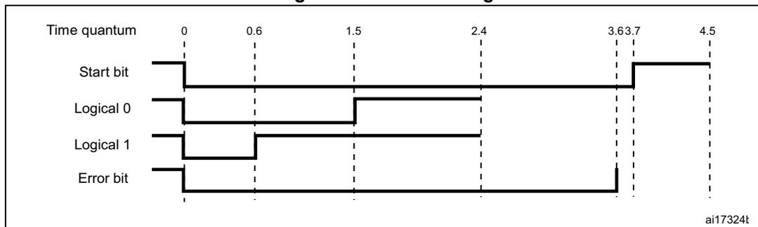
The diagram illustrates the timing for four types of bits: Start bit, Logical 0, Logical 1, and Error bit. The horizontal axis represents time quanta with markers at 0, 0.6, 1.5, 2.4, 3.6, 3.7, and 4.5. - Start bit : Signal goes low at 0 and returns high at 3.7 quanta. - Logical 0 : Signal goes low at 0 and returns high at 1.5 quanta. - Logical 1 : Signal goes low at 0 and returns high at 0.6 quanta. - Error bit : Signal goes low at 0 and returns high at 3.6 quanta. All bits end at 4.5 quanta.
24.7.6 CEC arbiter
The STM32F100xx CEC arbiter declines SFT and header arbitration techniques in the following cases:
- • CEC is a previous initiator retrying a failed transmission and
- a) the leading edge of the start bit is detected before SFT = 9.6 ms. This only occurs when a new initiator violates the SFT requirement. In this case CEC automatically synchronizes to the end of the transmitted start bit and participates in the header arbitration.
- b) CEC initiates frame transmission after 4 nominal bit times (9.6 ms) of the signal free time condition. CEC automatically switches to follower in case arbitration is lost (even though no contending device is expected in this case).
- • CEC is a new initiator that needs to send a frame and
- a) the leading edge of the start bit is detected before SFT = 5 minimum bit times (10.3 ms). This typically occurs when the previous initiator retries a failed transmission. In this case, CEC automatically switches to reception. Transmission is retried after the current frame.
- b) the leading edge of the start bit is detected when SFT is between 10.3 ms and 14.4 ms. This is usually caused by a different initiator contending the CEC line. STM32 CEC automatically synchronizes to the end of the transmitted start bit and participates in the header arbitration.
- c) CEC initiates frame transmission after 6 nominal bit times (14.4 ms) of the signal free time condition. It automatically switches to follower in case the arbitration is lost.
- • CEC is the last initiator that has to send a frame immediately after its previous frame and
- a) the leading edge of the start bit is detected before SFT = 7 minimum bit times (14.4 ms). This is caused by a new initiator. CEC automatically switches to reception and transmission is retried after the current frame, when CEC is no longer the last initiator.
- b) the leading edge of the start bit is detected when SFT is between 14.4 ms and 19.2 ms. This might be caused by a new late initiator. CEC automatically synchronizes to the end of the transmitted start bit and participates in the header arbitration.
- c) CEC initiates frame transmission after 8 nominal bit times (19.2 ms) of the signal free time condition. CEC automatically switches to follower if the arbitration is lost (even though no contending device is expected in this case).
Table 139. STM32 CEC arbitration
| SFT (ms) | < 9.6 | < 10.3 | < 14.4 | < 19.2 | ≥ 19.2 |
|---|---|---|---|---|---|
| Same initiator retrying failed transmission | enter arbitration | frame started | |||
| New initiator | switch to reception | enter arbitration | frame started | ||
| Same initiator has to send another frame | switch to reception | enter arbitration | frame started | ||
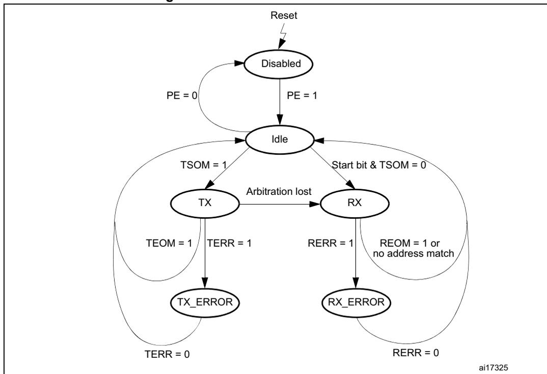
24.7.7 CEC states
Figure 279 shows the CEC controller state machine.
Figure 279. CEC control state machine
stateDiagram-v2
    [*] --> Disabled : Reset
    Disabled --> Idle : PE = 1
    Idle --> Disabled : PE = 0
    Idle --> TX : TSOM = 1
    Idle --> RX : Start bit & TSOM = 0
    TX --> Idle : Arbitration lost
    TX --> TX_ERROR : TEOM = 1
    TX --> TX_ERROR : TERR = 1
    TX --> Idle : TERR = 0
    RX --> Idle : REOM = 1 or no address match
    RX --> RX_ERROR : RERR = 1
    RX --> Idle : RERR = 0
The diagram illustrates the CEC control state machine with six states: Disabled, Idle, TX, RX, TX_ERROR, and RX_ERROR. Transitions are triggered by specific conditions:
- Disabled to Idle: Triggered by PE = 1.
- Idle to Disabled: Triggered by PE = 0.
- Idle to TX: Triggered by TSOM = 1.
- Idle to RX: Triggered by Start bit & TSOM = 0.
- TX to Idle: Triggered by Arbitration lost.
- TX to TX_ERROR: Triggered by TEOM = 1 or TERR = 1.
- TX to Idle: Triggered by TERR = 0.
- RX to Idle: Triggered by REOM = 1 or no address match.
- RX to RX_ERROR: Triggered by RERR = 1.
- RX to Idle: Triggered by RERR = 0.
The CEC controller assumes one of the six states described below:
Disabled state
The Disabled state is entered either on an APB reset or on resetting the PE bit in the CEC configuration register. Any ongoing transmission or reception is not interrupted and completes normally. The controller actually switches to Disabled when the PE bit is read back as 0. While the controller is in the Disabled state, activity on the CEC line is ignored and the clock prescaler is stopped for minimum power consumption purposes. The controller exits the Disabled state when the PE bit is set.
Idle state
The Idle state is entered whenever a message was transmitted or received successfully, or an error was processed. While in the Idle state, the CEC controller waits for either a transmit request (TSOM bit is set in the control status register) or a start bit.
RX state
The CEC controller enters the RX state when a start bit is detected and no message is pending for transmission. Once the header has been received, the destination address is compared to the value programmed in the own address register. If the two do not match and the address is not the broadcast address 0xF, the block is not acknowledged and the controller reverts to the Idle state. Otherwise, in case of a match, the controller remains in the RX state where the host CPU is requested to retrieve all message bytes from the RX buffer one by one. An available byte is signaled by the RBTTF bit being set in the control
status register. The host CPU can either poll this register or enable interrupts in the configuration status register to know whether a byte was received. If the RBTF bit is not cleared by the time a new block is received, the newly received block is not acknowledged to force the initiator to restart the message transmission, thus giving the host CPU a second chance to retrieve all message bytes in time. Note that it is the responsibility of the software driver to ignore messages where the number of operands is less than the number specified for the opcode.
The figure below shows an example of a complete message reception.
Figure 280. Example of a complete message reception
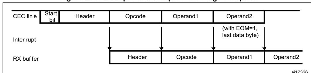
The diagram illustrates the flow of data from the CEC line to the RX buffer. On the CEC line, the sequence is: Start bit, Header, Opcode, Operand1, and Operand2. Interrupts are generated when the Header, Opcode, and Operand2 (marked as the last data byte with EOM=1) are received. The RX buffer captures the Header, Opcode, Operand1, and Operand2 in sequence. A small note 'ai17326' is present in the bottom right corner of the diagram area.
The software has to respect the sequence described in the table below.
Table 140. Software sequence to respect when receiving a message
| Software sequences | CEC_CSR register R/W access | Status bits | |||
|---|---|---|---|---|---|
| RTBF bit 7 | RERR bit 6 | REOM bit 5 | RSOM bit 4 | ||
| Poll RBTF or wait until an interrupt occurs | Read 0x00 | 0 | 0 | 0 | 0 |
| A header is received (RTBF and RSOM are set) | Read 0x90 or 0x91 (1) | 1 | 0 | 0 | 1 |
| Read header from RX buffer | - | 1 | 0 | 0 | 1 |
| Acknowledge received byte by writing 0x00 | Write 0x00 | 0 | 0 | 0 | 0 |
| Poll RBTF or wait until an interrupt occurs | Read 0x00 | 0 | 0 | 0 | 0 |
| An opcode is received (RBTF is set) | Read 0x80 or 0x81 | 1 | 0 | 0 | 0 |
| Read opcode from RX buffer | - | 1 | 0 | 0 | 0 |
| Acknowledge received byte by writing 0x00 | Write 0x00 | 0 | 0 | 0 | 0 |
| Poll RBTF or wait until an interrupt occurs | Read 0x00 | 0 | 0 | 0 | 0 |
| An operand is received (RBTF is set) | Read 0x80 or 0x81 | 1 | 0 | 0 | 0 |
| Read Operand1 from RX buffer | - | 1 | 0 | 0 | 0 |
| Acknowledge received byte by writing 0x00 | Write 0x00 | 0 | 0 | 0 | 0 |
| Poll RBTF or wait until an interrupt occurs | Read 0x00 | 0 | 0 | 0 | 0 |
| An operand is received, which is the last data byte (RBTF and REOM are set) | Read 0xA0 or 0xA1 | 1 | 0 | 1 | 0 |
| Read Operand2 from RX buffer | - | 1 | 0 | 1 | 0 |
| Acknowledge received byte by writing 0x00 | Write 0x00 | 0 | 0 | 0 | 0 |
1. Two different values may be read from the control and status register since a message may have queued for transmission but arbitration has been lost.
TX state
The controller enters the TX state when the TSOM bit is set in the control status register. In this state, it has to make sure that the required signal free time elapses before generating a start bit. That is, it has to wait for 9.6 ms if the previous state was TX_ERROR, 14.4 ms if the device was previously receiving, 19.2 ms otherwise. This wait count is however abandoned if another device transmits a start bit. At this point the CEC arbiter decides whether to switch to reception or to participate in the arbitration phase. Note that it is the responsibility of the software driver to send an initiator address consistent with the logical address programmed in the own address register.
Arbitration is lost if the received initiator address, contained in the least significant nibble of the shift register, differs from the initiator address still present in the TX buffer. In this case, the controller switches to the RX state immediately. After the receive phase, it however automatically retries transmitting until it is granted ownership of the bus.
If arbitration is not lost, a new byte should be written to the TX buffer each time the TBTRF bit is set in the control status register. The host CPU can either poll the control register or enable interrupts in the configuration register, to know whether a byte was transmitted. If it does not achieve the required task on time, a transmit error flag is set. The TEOM bit is set in the control status register to indicate that the message transmission was successful, but if the TERR bit is set in the control status register, the message should be considered lost.
The following shows an example of a complete message transmission.
Figure 281. Example of a complete message transmission
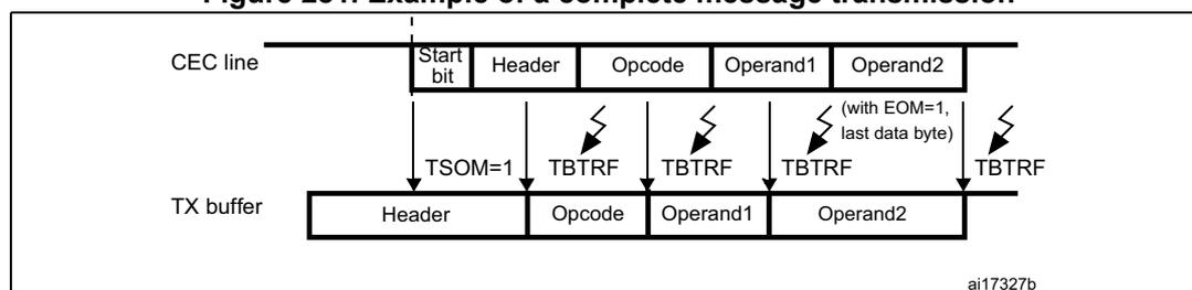
The diagram illustrates the timing of a message transmission. The top part shows the CEC line with a 'Start bit' followed by 'Header', 'Opcode', 'Operand1', and 'Operand2'. The bottom part shows the TX buffer with 'Header', 'Opcode', 'Operand1', and 'Operand2'. Arrows indicate the sequence of events: 'TSOM=1' is set at the start, and 'TBTRF' is set after each byte is transmitted. The last byte, 'Operand2', is marked with '(with EOM=1, last data byte)'.
The software must respect the sequence described below.
Table 141. Software sequence to respect when transmitting a message
| Software sequences | CEC_CSR R/W access | Status bits | |||
|---|---|---|---|---|---|
| TBTRF bit 3 | TERR bit 2 | TEOM bit 1 | TSOM bit 0 | ||
| Write header to TX buffer | - | 0 | 0 | 0 | 0 |
| Initiate message transmission by writing TSOM=1 | Write 0x01 | 0 | 0 | 0 | 1 |
| Poll TBTRF or wait until an interrupt occurs | Read 0x01/0x00 | 0 | 0 | 0 | 1 then 0 |
| The TX buffer is empty (TBTRF is set) | Read 0x08 | 1 | 0 | 0 | 0 |
| Write opcode to TX buffer | - | 1 | 0 | 0 | 0 |
| Acknowledge byte request by writing 0x00 | Write 0x00 | 0 | 0 | 0 | 0 |
| Poll TBTRF or wait until an interrupt occurs | Read 0x00 | 0 | 0 | 0 | 0 |
| The TX buffer is empty (TBTRF is set) | Read 0x08 | 1 | 0 | 0 | 0 |
Table 141. Software sequence to respect when transmitting a message (continued)
| Software sequences | CEC_CSR R/W access | Status bits | |||
|---|---|---|---|---|---|
| TBTRF bit 3 | TERR bit 2 | TEOM bit 1 | TSOM bit 0 | ||
| Write Operand1 to TX buffer | - | 1 | 0 | 0 | 0 |
| Acknowledge byte request by writing 0x00 | Write 0x00 | 0 | 0 | 0 | 0 |
| Poll TBTRF or wait until an interrupt occurs | Read 0x00 | 0 | 0 | 0 | 0 |
| Write Operand2 to TX buffer | - | 1 | 0 | 0 | 0 |
| Acknowledge byte request and signal end of message | Write 0x02 | 0 | 0 | 1 | 0 |
| Poll TBTRF or wait until an interrupt occurs | Read 0x00 | 0 | 0 | 0 | 0 |
| Message transmission is completed (TBTRF and TEOM are set) | Read 0x0A | 1 | 0 | 1 | 0 |
| Acknowledge successful completion by writing 0x0 | Write 0x0 | 0 | 0 | 0 | 0 |
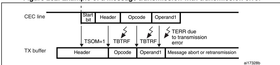
TX_ERROR state
The TX_ERROR state is entered if one of the following error conditions occurs:
- • a directly addressed message block is not acknowledged or a broadcast message block is negatively acknowledged (acknowledge error)
- • the TBTRF bit is not cleared while the requested byte needs to be transmitted (TBTFE error)
- • an unexpected bit is detected by the bit timing checker/generator (line error)
No error signalling mechanism is specified for the initiator, therefore no specific action is undertaken apart from aborting the current message and clearing the transmit request flag TSOM. The error handler decides if retransmission is possible depending on whether transmission has already failed six times or not. It also sets the transmit request flag if required.
The controller remains in the TX_ERROR state until the transmit error flag TERR is cleared. It then waits for an interframe spacing of 2 bit times before of being ready to process the next message.
An example of a message transmission with errors follows.
Figure 282. Example of a message transmission with transmission error
The software must respect the following sequence in case of a transmission error:
Table 142. Software sequence to respect when transmitting a message
| Software sequences | CEC_CSR R/W access | Status bits | |||
|---|---|---|---|---|---|
| TBTRF bit 3 | TERR bit 2 | TEOM bit 1 | TSOM bit 0 | ||
| Write header to TX buffer | - | 0 | 0 | 0 | 0 |
| Initiate message transmission by writing TSOM=1 | Write 0x01 | 0 | 0 | 0 | 1 |
| Poll TBTRF or wait until an interrupt occurs | Read 0x00/0x01 | 0 | 0 | 0 | 1 then 0 |
| The TX buffer is empty (TBTRF is set) | Read 0x08 | 1 | 0 | 0 | 0 |
| Write opcode to TX buffer | - | 1 | 0 | 0 | 0 |
| Acknowledge byte request by writing 0x00 | Write 0x00 | 0 | 0 | 0 | 0 |
| Poll TBTRF or wait until an interrupt occurs | Read 0x00 | 0 | 0 | 0 | 0 |
| The TX buffer is empty (TBTRF is set) | Read 0x08 | 1 | 0 | 0 | 0 |
| Write Operand1 to TX buffer | - | 1 | 0 | 0 | 0 |
| Acknowledge byte request by writing 0x00 | Write 0x00 | 0 | 0 | 0 | 0 |
| Poll TBTRF or wait until an interrupt occurs | Read 0x00 | 0 | 0 | 0 | 0 |
| The TX buffer is empty (TBTRF is set) | Read 0x08 | 1 | 0 | 0 | 0 |
| Write Operand2 to TX buffer | - | 1 | 0 | 0 | 0 |
| Acknowledge byte request and signal end of message | Write 0x02 | 0 | 0 | 1 | 0 |
| Poll TBTRF or wait until an interrupt occurs | Read 0x00 | 0 | 0 | 0 | 0 |
| Message transmission is completed (TBTRF and TEOM are set) | Read 0x0E | 1 | 1 | 1 | 0 |
| If TERR=1, read error code from error status register | - | 1 | 1 | 1 | 0 |
| Load header for retransmission if less than 5 retries | - | 1 | 1 | 1 | 0 |
| Acknowledge error and possibly request retransmission | Write 0x00 or 0x01 | 0 | 0 | 0 | 0/1 |
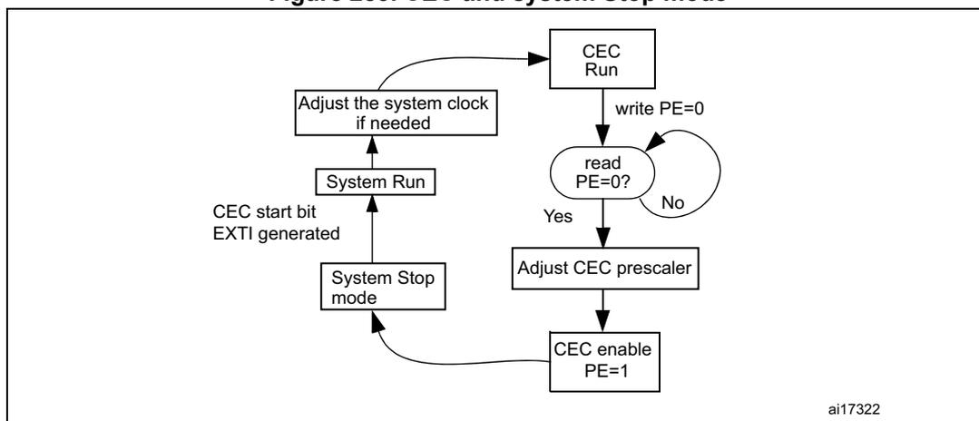
24.7.8 CEC and system Stop mode
Each time the application does not have anything left to transmit on the CEC line, the system can switch to the low-power Stop mode while waiting for a CEC message.
After wakeup from Stop mode the system runs on the HSI oscillator and the Start bit tolerance is 200 µs. So, the application only has 200 µs to restore the system clock, if needed. You can then choose to clock the system by PLL (with the HSI as the PLL source), or, let the system run on the HSI. In both cases, the CEC prescaler has to be re-adjusted, if needed, before entering the Stop mode.
To switch the system to the low-power Stop mode, and then wake it up on receiving new CEC data without losing the received data, execute the following procedure:
- 1. Perform a write clear to the peripheral enable (PE) bit in the CEC configuration register, then read back the PE bit value until it is seen at 0. The hardware clears the PE bit
when the current frame (if any) transmission is complete. Once PE is cleared, the HDMI-CEC peripheral is disabled and the CEC line signal is ignored. This operation ensures that the device safely enters the system Stop mode. Otherwise the system clock might stop while the CEC device is in the low impedance state, for example during a handshake bit. In such a case the CEC line gets stuck, causing all of the CEC nodes to be blocked in a stalled condition.
- 2. Write the CEC prescaler register according to the selected clock you want to use when the system woken up from the Stop mode.
- 3. Enable the CEC peripheral (PE = 1).
- 4. Configure the CEC line to generate an external asynchronous interrupt on the falling edge, to wake up the system upon detection of the leading edge of the next start bit.
- 5. Enter the system Stop mode. The system clock shuts down.
- 6. When the EXTI falling edge is detected, the system resumes from Stop mode. The STM32F100xx system wakeup is fast enough to allow correct start bit detection.
For more details on CEC wakeup from Stop mode refer to the AN3127: “CEC networking using STM32F100xx value line microcontrollers”.
Figure 283. CEC and system Stop mode
graph TD
    SR[System Run] --> AS[Adjust the system clock if needed]
    SR --> CR[CEC Run]
    CR --> WPE0[write PE=0]
    WPE0 --> RPE0{read PE=0?}
    RPE0 -- No --> RPE0
    RPE0 -- Yes --> AC[Adjust CEC prescaler]
    AC --> CEP1[CEC enable PE=1]
    CEP1 --> SM[System Stop mode]
    SM --> CE[CEC start bit EXTI generated]
    CE --> SR
24.8 HDMI-CEC interrupts
An interrupt can be produced:
- • during reception if a receive block transfer completes or if a receive error occurs
- • during transmission if a Transmit block transfer completes or if a transmit error occurs
Table 143. HDMI-CEC interrupts
| Interrupt event | Event flag | Enable control bit |
|---|---|---|
| Receive byte/block transfer finished | RBTF | IE |
| Receive error | RERR | IE |
| Transmit byte request or block transfer finished | TBTRF | IE |
| Transmit error | TERR | IE |
24.9 HDMI-CEC registers
Refer to Section 1.1 on page 32 for a list of abbreviations used in register descriptions.
The peripheral registers can be accessed by half-words (16-bit) or words (32-bit).
24.9.1 CEC configuration register (CEC_CFGR)
This register is used to configure the HDMI-CEC controller.
Address offset: 0x00
Reset value: 0x0000 0000
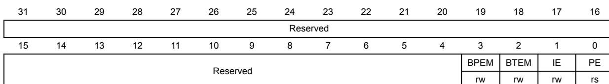
| 31 | 30 | 29 | 28 | 27 | 26 | 25 | 24 | 23 | 22 | 21 | 20 | 19 | 18 | 17 | 16 |
| Reserved | |||||||||||||||
| 15 | 14 | 13 | 12 | 11 | 10 | 9 | 8 | 7 | 6 | 5 | 4 | 3 | 2 | 1 | 0 |
| Reserved | BPEM | BTEM | IE | PE | |||||||||||
| rw | rw | rw | rs | ||||||||||||
Bits 31:4 Reserved, must be kept cleared.
Bit 3 BPEM : Bit period error mode
This bit is set/cleared by software.
0: Standard mode
1: Flexible bit-period mode
Bit 2 BTEM : Bit timing error mode
This bit is set/cleared by software.
0: Standard mode
1: Bit timing error-free mode
Bit 1 IE : Interrupt enable
This bit is set/cleared by software. It is used to activate an interrupt associated with the set of RTBF, RERR, TBTRF or TERR flags.
0: Interrupt disabled
1: Interrupt enabled
Bit 0 PE : Peripheral enable
This bit is set by software, cleared by hardware as soon as the CEC state is Idle.
0: Peripheral disabled
1: Peripheral enabled
24.9.2 CEC own address register (CEC_OAR)
This register is written by the software to define the address of the CEC device.
Address offset: 0x4
Reset value: 0x0000 0000
| 31 | 30 | 29 | 28 | 27 | 26 | 25 | 24 | 23 | 22 | 21 | 20 | 19 | 18 | 17 | 16 |
|---|---|---|---|---|---|---|---|---|---|---|---|---|---|---|---|
| Reserved | |||||||||||||||
| 15 | 14 | 13 | 12 | 11 | 10 | 9 | 8 | 7 | 6 | 5 | 4 | 3 | 2 | 1 | 0 |
| Reserved | OA[3:0] | ||||||||||||||
| rw | |||||||||||||||
Bits 31:4 Reserved, must be kept cleared.
Bits 3:0 OA[3:0] : Own address
These bits are written by software to define the own address of the CEC device.
Default value 0x0 is the TV address as defined in the HDMI specification.
24.9.3 CEC prescaler register (CEC_PRES)
This register is written by the software to reach the required bit time versus the APB clock frequency.
Address offset: 0x8
Reset value: 0x0000 0000
| 31 | 30 | 29 | 28 | 27 | 26 | 25 | 24 | 23 | 22 | 21 | 20 | 19 | 18 | 17 | 16 |
|---|---|---|---|---|---|---|---|---|---|---|---|---|---|---|---|
| Reserved | |||||||||||||||
| 15 | 14 | 13 | 12 | 11 | 10 | 9 | 8 | 7 | 6 | 5 | 4 | 3 | 2 | 1 | 0 |
| Reserved | PRESC[13:0] | ||||||||||||||
| rw | rw | rw | rw | rw | rw | rw | rw | rw | rw | rw | rw | rw | rw | ||
Bits 31:14 Reserved, must be kept cleared.
Bits 13:0 PRESC[13:0] : Prescaler counter value
These bits are written by software to adjust the internal prescaler counter to generate the required 50 µs time base.
PRESC must be selected to respect the following formula: \( PRESC = 50 \times f_{PCLK} \text{ (MHz)} - 1 \) where PRESC must be an integer.
Example: if \( f_{PCLK} = 24 \text{ MHz} \) , then PRESC must be programmed to 1199(0x4AF)
24.9.4 CEC error status register (CEC_ESR)
CEC_ESR is the CEC error status register. It contains all the error flags related to the communication.
Address offset: 0x0C
Reset value: 0x0000 0000
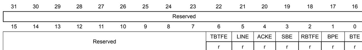
| 31 | 30 | 29 | 28 | 27 | 26 | 25 | 24 | 23 | 22 | 21 | 20 | 19 | 18 | 17 | 16 |
| Reserved | |||||||||||||||
| 15 | 14 | 13 | 12 | 11 | 10 | 9 | 8 | 7 | 6 | 5 | 4 | 3 | 2 | 1 | 0 |
| Reserved | TBTTFE | LINE | ACKE | SBE | RBTTFE | BPE | BTE | ||||||||
| r | r | r | r | r | r | r | r | ||||||||
Bits 31:7 Reserved, must be kept cleared.
Bit 6 TBTTFE : Tx block transfer finished error
This bit is set by hardware when the TBTTFE bit is not cleared while the requested byte needs to be transmitted.
It is cleared by software when clearing the TX error flag (TERR) of the CEC_CSR register.
Bit 5 LINE : Line error
This bit is set by hardware when the CEC line is detected low although it is driven to high impedance while not in the arbitration phase or during the ACK bit.
It is cleared by software by clearing the TX error flag (TERR) in the CEC_CSR register.
Bit 4 ACKE : Block acknowledge error
This bit is set by hardware when a directly addressed message block is not acknowledged or when a broadcast message block is negatively acknowledged.
It is cleared by software when clearing the TX error flag (TERR) or the Rx error flag (RERR) in the CEC_CSR register.
Bit 3 SBE : Start bit error
This bit is set by hardware when the start bit (identified by its low duration only, that is, an error bit), is detected before the end of a message.
It is cleared by software by clearing the Rx error flag (RERR) in the CEC_CSR register.
Bit 2 RBTTFE : Rx block transfer finished error
This bit is set by hardware when the RBTTFE bit is not cleared while a new byte is ready to be written to the RX buffer.
It is cleared by software by clearing the Rx error flag (RERR) in the CEC_CSR register.
Bit 1 BPE : Bit period error
This bit is set by hardware when the time between two falling edges on the CEC line is too short in Bit period error mode or out of specification in Safe mode, start bit excepted. It is not set if BTE was previously set.
It is cleared by software by clearing the Rx error flag (RERR) in the CEC_CSR register.
Bit 0 BTE : Bit timing error
This bit is set by hardware when an incorrect rising edge position is detected on the CEC line while in Safe mode, start bit excepted.
It is cleared by software by clearing the Rx error flag (RERR) in the CEC_CSR register.
24.9.5 CEC control and status register (CEC_CSR)
CEC_CSR is the CEC control & status register. It contains all the flags related to the communication and some control bits to be managed during the communication.
Address offset: 0x10
Reset value: 0x0000 0000
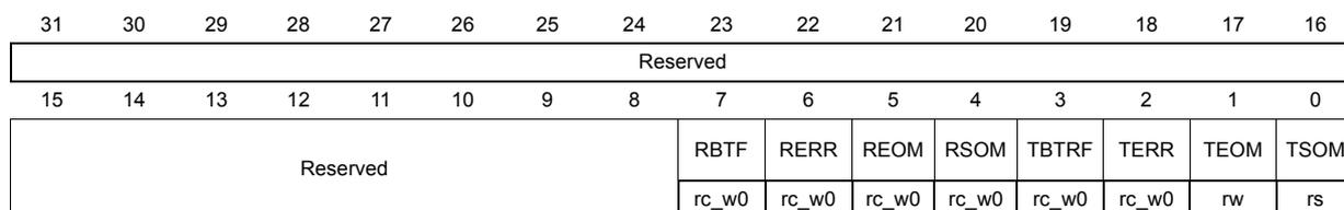
| 31 | 30 | 29 | 28 | 27 | 26 | 25 | 24 | 23 | 22 | 21 | 20 | 19 | 18 | 17 | 16 |
| Reserved | |||||||||||||||
| 15 | 14 | 13 | 12 | 11 | 10 | 9 | 8 | 7 | 6 | 5 | 4 | 3 | 2 | 1 | 0 |
| Reserved | RBTF | RERR | REOM | RSOM | TBTRF | TERR | TEOM | TSOM | |||||||
| rc_w0 | rc_w0 | rc_w0 | rc_w0 | rc_w0 | rc_w0 | rw | rs | ||||||||
Bits 31:8 Reserved, must be kept cleared.
Bit 7 RBTF : Rx byte/block transfer finished
This bit is set by hardware when a data byte has been received. If the IE bit in the CEC_CFGR register is set, an interrupt is generated.
It is cleared by software by writing it to 0 to acknowledge the event and clear the associated interrupt.
Bit 6 RERR : Rx error
This bit is set by hardware when a reception error occurs. The software can read the CEC_ESR register to better know which error occurred. If the IE bit in the CEC_CFGR register is set, an interrupt is generated.
It is cleared by software by writing it to 0 to acknowledge the error and clear the associated interrupt.
Bit 5 REOM : Rx end of message
This bit is set by hardware when the last data byte of a message has been received.
It is cleared by software by writing it to 0 to acknowledge the event.
Note: Do not clear the REOM bit before the RBTF flag/interrupt is set.
Bit 4 RSOM : Rx start of message
This bit is set by hardware when a header byte is received.
It is cleared by software by writing it to 0 to acknowledge the event.
Bit 3 TBTRF : Tx byte transfer request or block transfer finished
This bit is set by hardware either to request a new data byte when TEOM is not set or to signal the successful transmission of the message when TEOM is set. If the IE bit in the CEC_CFGR register is set, an interrupt is generated.
It is cleared by software by writing it to 0 to acknowledge the event and clear the associated interrupt.
Bit 2 TERR : Tx error
This bit is set by hardware when a transmission error occurs. The software can read the CEC_ESR register to better know which error occurred. If the IE bit in the CEC_CFGR register is set, an interrupt is generated.
It is cleared by software by writing it to 0 to acknowledge the error and clear the associated interrupt.
Bit 1 TEOM : Tx end of message
This bit is set and cleared by software except if RTBF or RERR is set.
0: the data byte will be transmitted without any EOM bit
1: the data byte will be transmitted with an EOM bit, signalling the end of the message
Bit 0 TSOM : Tx start of message
This bit is set by software to request transmission of a new message. The TX data byte is supposed to contain the header byte.
It is cleared by hardware when access to bus is granted or when a transmission error has occurred.
24.9.6 CEC Tx data register (CEC_TXD)
Address offset: 0x14
Reset value: 0x0000 0000
| 31 | 30 | 29 | 28 | 27 | 26 | 25 | 24 | 23 | 22 | 21 | 20 | 19 | 18 | 17 | 16 |
|---|---|---|---|---|---|---|---|---|---|---|---|---|---|---|---|
| Reserved | |||||||||||||||
| 15 | 14 | 13 | 12 | 11 | 10 | 9 | 8 | 7 | 6 | 5 | 4 | 3 | 2 | 1 | 0 |
| Reserved | TXD[7:0] | ||||||||||||||
| rw | |||||||||||||||
Bits 31:8 Reserved, must be kept cleared.
Bits 7:0 TXD[7:0] : Tx Data register.
Data byte to be transmitted.
24.9.7 CEC Rx data register (CEC_RXD)
Address offset: 0x18
Reset value: 0x0000 0000
| 31 | 30 | 29 | 28 | 27 | 26 | 25 | 24 | 23 | 22 | 21 | 20 | 19 | 18 | 17 | 16 |
|---|---|---|---|---|---|---|---|---|---|---|---|---|---|---|---|
| Reserved | |||||||||||||||
| 15 | 14 | 13 | 12 | 11 | 10 | 9 | 8 | 7 | 6 | 5 | 4 | 3 | 2 | 1 | 0 |
| Reserved | RXD[7:0] | ||||||||||||||
| r | |||||||||||||||
Bits 31:8 Reserved, must be kept cleared.
Bits 7:0 RXD[7:0] : Rx data register.
This is a read-only register which contains the last data byte that was received.
24.9.8 HDMI-CEC register map
The following table summarizes the HDMI-CEC registers.
Table 144. HDMI-CEC register map and reset values
| Offset | Register | 31 | 30 | 29 | 28 | 27 | 26 | 25 | 24 | 23 | 22 | 21 | 20 | 19 | 18 | 17 | 16 | 15 | 14 | 13 | 12 | 11 | 10 | 9 | 8 | 7 | 6 | 5 | 4 | 3 | 2 | 1 | 0 |
|---|---|---|---|---|---|---|---|---|---|---|---|---|---|---|---|---|---|---|---|---|---|---|---|---|---|---|---|---|---|---|---|---|---|
| 0x00 | CEC_CFGR | Reserved | BPEM | BTEM | IE | PE | |||||||||||||||||||||||||||
| Reset value | 0 | 0 | 0 | 0 | |||||||||||||||||||||||||||||
| 0x04 | CEC_OAR | Reserved | OAR[3:0] | ||||||||||||||||||||||||||||||
| Reset value | 0 | 0 | 0 | 0 | |||||||||||||||||||||||||||||
| 0x08 | CEC_PRE | Reserved | PRESC[13:0] | ||||||||||||||||||||||||||||||
| Reset value | 0 | 0 | 0 | 0 | 0 | 0 | 0 | 0 | 0 | 0 | 0 | 0 | 0 | 0 | |||||||||||||||||||
| 0x0C | CEC_ESR | Reserved | TBTFE | LINE | ACKE | SBE | RBTFE | BPE | BTE | ||||||||||||||||||||||||
| Reset value | 0 | 0 | 0 | 0 | 0 | 0 | 0 | ||||||||||||||||||||||||||
| 0x10 | CEC_CSR | Reserved | RBTF | RERR | REOM | RSOM | TBTRF | TERR | TEOM | TSOM | |||||||||||||||||||||||
| Reset value | 0 | 0 | 0 | 0 | 0 | 0 | 0 | 0 | |||||||||||||||||||||||||
| 0x14 | CEC_TXD | Reserved | TXD[7:0] | ||||||||||||||||||||||||||||||
| Reset value | 0 | 0 | 0 | 0 | 0 | 0 | 0 | 0 | |||||||||||||||||||||||||
| 0x18 | CEC_RXD | Reserved | RXD[7:0] | ||||||||||||||||||||||||||||||
| Reset value | 0 | 0 | 0 | 0 | 0 | 0 | 0 | 0 | |||||||||||||||||||||||||
Refer to Table 1 on page 37 and Table 2 on page 38 for the register boundary addresses.