21. Serial peripheral interface (SPI)
Low-density value line devices are STM32F100xx microcontrollers where the flash memory density ranges between 16 and 32 Kbytes.
Medium-density value line devices are STM32F100xx microcontrollers where the flash memory density ranges between 64 and 128 Kbytes.
High-density value line devices are STM32F100xx microcontrollers where the flash memory density ranges between 256 and 512 Kbytes.
21.1 SPI introduction
The serial peripheral interface (SPI) allows half/ full-duplex, synchronous, serial communication with external devices. The interface can be configured as the master and in this case it provides the communication clock (SCK) to the external slave device. The interface is also capable of operating in multimaster configuration.
It may be used for a variety of purposes, including simplex synchronous transfers on two lines with a possible bidirectional data line or reliable communication using CRC checking.
Warning: Since some SPI1 and SPI3 pins may be mapped onto some pins used by the JTAG interface (SPI1/3_NSS onto JTDI, SPI1/3_SCK onto JTDO and SPI1/3_MISO onto NJTRST), you may either:
- – disable the JTAG and use the SWD interface prior to configuring the pins listed as SPI IOs (when debugging the application), or
- – disable both JTAG/SWD interfaces (for standalone applications).
For more information on the configuration of the JTAG/SWD interface pins, refer to Section 7.3.3: JTAG/SWD alternate function remapping .
21.2 SPI main features
21.2.1 SPI features
- • Full-duplex synchronous transfers on three lines
- • Simplex synchronous transfers on two lines with or without a bidirectional data line
- • 8- or 16-bit transfer frame format selection
- • Master or slave operation
- • Multimaster mode capability
- • 8 master mode baud rate prescalers ( \( f_{PCLK}/2 \) max.)
- • Slave mode frequency ( \( f_{PCLK}/2 \) max)
- • Faster communication for both master and slave
- • NSS management by hardware or software for both master and slave: dynamic change of master/slave operations
- • Programmable clock polarity and phase
- • Programmable data order with MSB-first or LSB-first shifting
- • Dedicated transmission and reception flags with interrupt capability
- • SPI bus busy status flag
- • Hardware CRC feature for reliable communication:
- – CRC value can be transmitted as last byte in Tx mode
- – Automatic CRC error checking for last received byte
- • Master mode fault, overrun and CRC error flags with interrupt capability
- • 1-byte transmission and reception buffer with DMA capability: Tx and Rx requests
21.3 SPI functional description
21.3.1 General description
The block diagram of the SPI is shown in Figure 222 .
![Figure 222. SPI block diagram. This diagram illustrates the internal architecture of an SPI peripheral. On the left, four pins are shown: MOSI, MISO, SCK, and NSS. The MOSI and MISO pins are connected to a 'Shift register' block. Data is written to the shift register from a 'Tx buffer' (which receives data from the 'Address and data bus' via a 'Write' path) and is read from the shift register to an 'Rx buffer' (which then sends data to the 'Address and data bus' via a 'Read' path). The shift register is configured for 'LSB first' operation. The SCK pin is connected to a 'Baud rate generator' block, which is controlled by the 'BR[2:0]' bits in the SPI_CR1 register. The Master control logic block is connected to the SCK, NSS, and Address and data bus lines. The Communication control block is connected to the shift register, the baud rate generator, and the SPI registers (SPI_CR1, SPI_CR2, and SPI_SR). The SPI_CR1 register contains bits for LSB_FIRST, SPE, BR2, BR1, BR0, MSTR, CPOL, CPHA, BIDI_MODE, BIDI_OE, CRCEN, CRC_Next, DFF, RX_ONLY, SSM, and SSI. The SPI_CR2 register contains bits for TXE IE, RXNE IE, ERR IE, 0, 0, SSOE, TXDM AEN, and RXDM AEN. The SPI_SR register contains bits for BSY, OVR, MOD F, CRC ERR, 0, 0, TXE, and RXNE. The Address and data bus is a wide bus at the top of the diagram.](/RM0041-STM32F100/96769a052d805bd85391e6a7d58a0cd6_img.jpg)
Figure 222. SPI block diagram
Usually, the SPI is connected to external devices through four pins:
- • MISO: Master In / Slave Out data. This pin can be used to transmit data in slave mode and receive data in master mode.
- • MOSI: Master Out / Slave In data. This pin can be used to transmit data in master mode and receive data in slave mode.
- • SCK: Serial Clock output for SPI masters and input for SPI slaves.
- • NSS: Slave select. This is an optional pin to select a slave device. This pin acts as a 'chip select' to let the SPI master communicate with slaves individually and to avoid contention on the data lines. Slave NSS inputs can be driven by standard IO ports on the master device. The NSS pin may also be used as an output if enabled (SSOE bit) and driven low if the SPI is in master configuration. In this manner, all NSS pins from devices connected to the Master NSS pin see a low level and become slaves when they are configured in NSS hardware mode. When configured in master mode with NSS configured as an input (MSTR=1 and SSOE=0) and if NSS is pulled low, the SPI enters the master mode fault state: the MSTR bit is automatically cleared and the device is configured in slave mode (refer to Section 21.3.10 ).
A basic example of interconnections between a single master and a single slave is illustrated in Figure 223 .
Figure 223. Single master/ single slave application
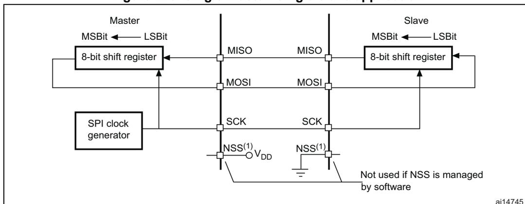
- 1. Here, the NSS pin is configured as an input.
The MOSI pins are connected together and the MISO pins are connected together. In this way data is transferred serially between master and slave (most significant bit first).
The communication is always initiated by the master. When the master device transmits data to a slave device via the MOSI pin, the slave device responds via the MISO pin. This implies full-duplex communication with both data out and data in synchronized with the same clock signal (which is provided by the master device via the SCK pin).
Slave select (NSS) pin management
Hardware or software slave select management can be set using the SSM bit in the SPI_CR1 register.
- • Software NSS management (SSM = 1)
The slave select information is driven internally by the value of the SSI bit in the SPI_CR1 register. The external NSS pin remains free for other application uses.
- • Hardware NSS management (SSM = 0)
Two configurations are possible depending on the NSS output configuration (SSOE bit in register SPI_CR2).
- – NSS output enabled (SSM = 0, SSOE = 1)
This configuration is used only when the device operates in master mode. The NSS signal is driven low when the master starts the communication and is kept low until the SPI is disabled.
- – NSS output disabled (SSM = 0, SSOE = 0)
This configuration allows multimaster capability for devices operating in master mode. For devices set as slave, the NSS pin acts as a classical NSS input: the slave is selected when NSS is low and deselected when NSS high.
Clock phase and clock polarity
Four possible timing relationships may be chosen by software, using the CPOL and CPHA bits in the SPI_CR1 register. The CPOL (clock polarity) bit controls the steady state value of the clock when no data is being transferred. This bit affects both master and slave modes. If CPOL is reset, the SCK pin has a low-level idle state. If CPOL is set, the SCK pin has a high-level idle state.
If the CPHA (clock phase) bit is set, the second edge on the SCK pin (falling edge if the CPOL bit is reset, rising edge if the CPOL bit is set) is the MSBit capture strobe. Data are latched on the occurrence of the second clock transition. If the CPHA bit is reset, the first edge on the SCK pin (falling edge if CPOL bit is set, rising edge if CPOL bit is reset) is the MSBit capture strobe. Data are latched on the occurrence of the first clock transition.
The combination of the CPOL (clock polarity) and CPHA (clock phase) bits selects the data capture clock edge.
Figure 224 , shows an SPI transfer with the four combinations of the CPHA and CPOL bits. The diagram may be interpreted as a master or slave timing diagram where the SCK pin, the MISO pin, the MOSI pin are directly connected between the master and the slave device.
Note:
Prior to changing the CPOL/CPHA bits the SPI must be disabled by resetting the SPE bit.
Master and slave must be programmed with the same timing mode.
The idle state of SCK must correspond to the polarity selected in the SPI_CR1 register (by pulling up SCK if CPOL=1 or pulling down SCK if CPOL=0).
The Data Frame Format (8- or 16-bit) is selected through the DFF bit in SPI_CR1 register, and determines the data length during transmission/reception.
Figure 224. Data clock timing diagram
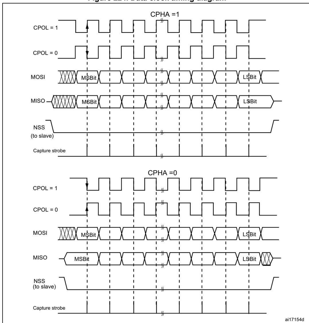
The figure illustrates the timing of SPI data transfer for two phases (CPHA = 1 and CPHA = 0). For each phase, two clock polarities (CPOL = 1 and CPOL = 0) are shown. The MOSI and MISO signals are shown as a series of bits, with the MSBit and LSBit indicated. The NSS signal is shown as a series of pulses. The Capture strobe is shown as a series of pulses. The diagram is labeled ai17154d.
- 1. These timings are shown with the LSBFIRST bit reset in the SPI_CR1 register.
Data frame format
Data can be shifted out either MSB-first or LSB-first depending on the value of the LSBFIRST bit in the SPI_CR1 register.
Each data frame is 8 or 16 bits long depending on the size of the data programmed using the DFF bit in the SPI_CR1 register. The selected data frame format is applicable for transmission and/or reception.
21.3.2 Configuring the SPI in slave mode
In the slave configuration, the serial clock is received on the SCK pin from the master device. The value set in the BR[2:0] bits in the SPI_CR1 register, does not affect the data transfer rate.
Note: It is recommended to enable the SPI slave before the master sends the clock. If not, undesired data transmission might occur. The data register of the slave needs to be ready before the first edge of the communication clock or before the end of the ongoing communication. It is mandatory to have the polarity of the communication clock set to the steady state value before the slave and the master are enabled.
Follow the procedure below to configure the SPI in slave mode:
Procedure
- 1. Set the DFF bit to define 8- or 16-bit data frame format
- 2. Select the CPOL and CPHA bits to define one of the four relationships between the data transfer and the serial clock (see Figure 224 ). For correct data transfer, the CPOL and CPHA bits must be configured in the same way in the slave device and the master device.
- 3. The frame format (MSB-first or LSB-first depending on the value of the LSBFIRST bit in the SPI_CR1 register) must be the same as the master device.
- 4. In Hardware mode (refer to Slave select (NSS) pin management ), the NSS pin must be connected to a low level signal during the complete byte transmit sequence. In NSS software mode, set the SSM bit and clear the SSI bit in the SPI_CR1 register.
- 5. Clear the MSTR bit and set the SPE bit (both in the SPI_CR1 register) to assign the pins to alternate functions.
In this configuration the MOSI pin is a data input and the MISO pin is a data output.
Transmit sequence
The data byte is parallel-loaded into the Tx buffer during a write cycle.
The transmit sequence begins when the slave device receives the clock signal and the most significant bit of the data on its MOSI pin. The remaining bits (the 7 bits in 8-bit data frame format, and the 15 bits in 16-bit data frame format) are loaded into the shift-register. The TXE flag in the SPI_SR register is set on the transfer of data from the Tx Buffer to the shift register and an interrupt is generated if the TXEIE bit in the SPI_CR2 register is set.
Receive sequence
For the receiver, when data transfer is complete:
- • The Data in shift register is transferred to Rx Buffer and the RXNE flag (SPI_SR register) is set
- • An Interrupt is generated if the RXNEIE bit is set in the SPI_CR2 register.
After the last sampling clock edge the RXNE bit is set, a copy of the data byte received in the shift register is moved to the Rx buffer. When the SPI_DR register is read, the SPI peripheral returns this buffered value.
Clearing of the RXNE bit is performed by reading the SPI_DR register.
21.3.3 Configuring the SPI in master mode
In the master configuration, the serial clock is generated on the SCK pin.
Procedure
- 1. Select the BR[2:0] bits to define the serial clock baud rate (see SPI_CR1 register).
- 2. Select the CPOL and CPHA bits to define one of the four relationships between the data transfer and the serial clock (see Figure 224 ).
- 3. Set the DFF bit to define 8- or 16-bit data frame format
- 4. Configure the LSBFIRST bit in the SPI_CR1 register to define the frame format.
- 5. If the NSS pin is required in input mode, in hardware mode, connect the NSS pin to a high-level signal during the complete byte transmit sequence. In NSS software mode, set the SSM and SSI bits in the SPI_CR1 register. If the NSS pin is required in output mode, the SSOE bit only should be set.
- 6. The MSTR and SPE bits must be set (they remain set only if the NSS pin is connected to a high-level signal).
In this configuration the MOSI pin is a data output and the MISO pin is a data input.
Transmit sequence
The transmit sequence begins when a byte is written in the Tx Buffer.
The data byte is parallel-loaded into the shift register (from the internal bus) during the first bit transmission and then shifted out serially to the MOSI pin MSB first or LSB first depending on the LSBFIRST bit in the SPI_CR1 register. The TXE flag is set on the transfer of data from the Tx Buffer to the shift register and an interrupt is generated if the TXEIE bit in the SPI_CR2 register is set.
Receive sequence
For the receiver, when data transfer is complete:
- • The data in the shift register is transferred to the RX Buffer and the RXNE flag is set
- • An interrupt is generated if the RXNEIE bit is set in the SPI_CR2 register
At the last sampling clock edge the RXNE bit is set, a copy of the data byte received in the shift register is moved to the Rx buffer. When the SPI_DR register is read, the SPI peripheral returns this buffered value.
Clearing the RXNE bit is performed by reading the SPI_DR register.
A continuous transmit stream can be maintained if the next data to be transmitted is put in the Tx buffer once the transmission is started. Note that TXE flag should be '1 before any attempt to write the Tx buffer is made.
Note: When a master is communicating with SPI slaves which need to be de-selected between transmissions, the NSS pin must be configured as GPIO or another GPIO must be used and toggled by software.
21.3.4 Configuring the SPI for half-duplex communication
The SPI is capable of operating in half-duplex mode in 2 configurations.
- • 1 clock and 1 bidirectional data wire
- • 1 clock and 1 data wire (receive-only or transmit-only)
1 clock and 1 bidirectional data wire (BIDIMODE = 1)
This mode is enabled by setting the BIDIMODE bit in the SPI_CR1 register. In this mode SCK is used for the clock and MOSI in master or MISO in slave mode is used for data communication. The transfer direction (Input/Output) is selected by the BIDIOE bit in the SPI_CR1 register. When this bit is 1, the data line is output otherwise it is input.
1 clock and 1 unidirectional data wire (BIDIMODE = 0)
In this mode, the application can use the SPI either in transmit-only mode or in receive-only mode.
- • Transmit-only mode is similar to full-duplex mode (BIDIMODE=0, RXONLY=0): the data are transmitted on the transmit pin (MOSI in master mode or MISO in slave mode) and the receive pin (MISO in master mode or MOSI in slave mode) can be used as a general-purpose IO. In this case, the application just needs to ignore the Rx buffer (if the data register is read, it does not contain the received value).
- • In receive-only mode, the application can disable the SPI output function by setting the RXONLY bit in the SPI_CR1 register. In this case, it frees the transmit IO pin (MOSI in master mode or MISO in slave mode), so it can be used for other purposes.
To start the communication in receive-only mode, configure and enable the SPI:
- • In master mode, the communication starts immediately and stops when the SPE bit is cleared and the current reception stops. There is no need to read the BSY flag in this mode. It is always set when an SPI communication is ongoing.
- • In slave mode, the SPI continues to receive as long as the NSS is pulled down (or the SSI bit is cleared in NSS software mode) and the SCK is running.
21.3.5 Data transmission and reception procedures
Rx and Tx buffers
In reception, data are received and then stored into an internal Rx buffer while In transmission, data are first stored into an internal Tx buffer before being transmitted.
A read access of the SPI_DR register returns the Rx buffered value whereas a write access to the SPI_DR stores the written data into the Tx buffer.
Start sequence in master mode
- • In full-duplex (BIDIMODE=0 and RXONLY=0)
- – The sequence begins when data are written into the SPI_DR register (Tx buffer).
- – The data are then parallel loaded from the Tx buffer into the 8-bit shift register during the first bit transmission and then shifted out serially to the MOSI pin.
- – At the same time, the received data on the MISO pin is shifted in serially to the 8-bit shift register and then parallel loaded into the SPI_DR register (Rx buffer).
- • In unidirectional receive-only mode (BIDIMODE=0 and RXONLY=1)
- – The sequence begins as soon as SPE=1
- – Only the receiver is activated and the received data on the MISO pin are shifted in serially to the 8-bit shift register and then parallel loaded into the SPI_DR register (Rx buffer).
- • In bidirectional mode, when transmitting (BIDIMODE=1 and BIDIOE=1)
- – The sequence begins when data are written into the SPI_DR register (Tx buffer).
- – The data are then parallel loaded from the Tx buffer into the 8-bit shift register during the first bit transmission and then shifted out serially to the MOSI pin.
- – No data are received.
- • In bidirectional mode, when receiving (BIDIMODE=1 and BIDIOE=0)
- – The sequence begins as soon as SPE=1 and BIDIOE=0.
- – The received data on the MOSI pin are shifted in serially to the 8-bit shift register and then parallel loaded into the SPI_DR register (Rx buffer).
- – The transmitter is not activated and no data are shifted out serially to the MOSI pin.
Start sequence in slave mode
- • In full-duplex mode (BIDIMODE=0 and RXONLY=0)
- – The sequence begins when the slave device receives the clock signal and the first bit of the data on its MOSI pin. The 7 remaining bits are loaded into the shift register.
- – At the same time, the data are parallel loaded from the Tx buffer into the 8-bit shift register during the first bit transmission, and then shifted out serially to the MISO pin. The software must have written the data to be sent before the SPI master device initiates the transfer.
- • In unidirectional receive-only mode (BIDIMODE=0 and RXONLY=1)
- – The sequence begins when the slave device receives the clock signal and the first bit of the data on its MOSI pin. The 7 remaining bits are loaded into the shift register.
- – The transmitter is not activated and no data are shifted out serially to the MISO pin.
- • In bidirectional mode, when transmitting (BIDIMODE=1 and BIDIOE=1)
- – The sequence begins when the slave device receives the clock signal and the first bit in the Tx buffer is transmitted on the MISO pin.
- – The data are then parallel loaded from the Tx buffer into the 8-bit shift register during the first bit transmission and then shifted out serially to the MISO pin. The
software must have written the data to be sent before the SPI master device initiates the transfer.
- – No data are received.
- • In bidirectional mode, when receiving (BIDIMODE=1 and BIDIOE=0)
- – The sequence begins when the slave device receives the clock signal and the first bit of the data on its MISO pin.
- – The received data on the MISO pin are shifted in serially to the 8-bit shift register and then parallel loaded into the SPI_DR register (Rx buffer).
- – The transmitter is not activated and no data are shifted out serially to the MISO pin.
Handling data transmission and reception
The TXE flag (Tx buffer empty) is set when the data are transferred from the Tx buffer to the shift register. It indicates that the internal Tx buffer is ready to be loaded with the next data. An interrupt can be generated if the TXEIE bit in the SPI_CR2 register is set. Clearing the TXE bit is performed by writing to the SPI_DR register.
Note: The software must ensure that the TXE flag is set to 1 before attempting to write to the Tx buffer. Otherwise, it overwrites the data previously written to the Tx buffer.
The RXNE flag (Rx buffer not empty) is set on the last sampling clock edge, when the data are transferred from the shift register to the Rx buffer. It indicates that data are ready to be read from the SPI_DR register. An interrupt can be generated if the RXNEIE bit in the SPI_CR2 register is set. Clearing the RXNE bit is performed by reading the SPI_DR register.
For some configurations, the BSY flag can be used during the last data transfer to wait until the completion of the transfer.
Full-duplex transmit and receive procedure in master or slave mode (BIDIMODE=0 and RXONLY=0)
The software has to follow this procedure to transmit and receive data (see Figure 225 and Figure 226 ):
- 1. Enable the SPI by setting the SPE bit to 1.
- 2. Write the first data item to be transmitted into the SPI_DR register (this clears the TXE flag).
- 3. Wait until TXE=1 and write the second data item to be transmitted. Then wait until RXNE=1 and read the SPI_DR to get the first received data item (this clears the RXNE bit). Repeat this operation for each data item to be transmitted/received until the n–1 received data.
- 4. Wait until RXNE=1 and read the last received data.
- 5. Wait until TXE=1 and then wait until BSY=0 before disabling the SPI.
This procedure can also be implemented using dedicated interrupt subroutines launched at each rising edges of the RXNE or TXE flag.
Figure 225. TXE/RXNE/BSY behavior in Master / full-duplex mode (BIDIMODE=0 and RXONLY=0) in case of continuous transfers
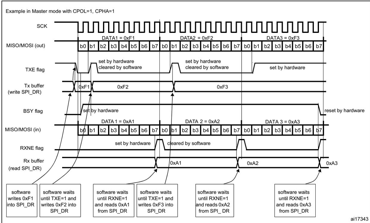
Example in Master mode with CPOL=1, CPHA=1
The diagram illustrates the timing and control signals for an SPI Master in full-duplex mode. The SCK signal is a continuous square wave. The MISO/MOSI (out) line transmits DATA1 = 0xF1, DATA2 = 0xF2, and DATA3 = 0xF3, each split into bytes b0-b7. The TXE flag is set by hardware when the Tx buffer is empty and cleared by software when data is written. The Tx buffer (write SPI_DR) contains the data to be transmitted. The BSY flag is set by hardware when the SPI is active and reset by hardware when it is inactive. The MISO/MOSI (in) line receives DATA 1 = 0xA1, DATA 2 = 0xA2, and DATA 3 = 0xA3, also split into bytes b0-b7. The RXNE flag is set by hardware when the Rx buffer is not empty and cleared by software when data is read. The Rx buffer (read SPI_DR) contains the received data. The software actions are: write 0xF1 into SPI_DR; wait until TXE=1 and write 0xF2 into SPI_DR; wait until RXNE=1 and read 0xA1 from SPI_DR; wait until TXE=1 and write 0xF3 into SPI_DR; wait until RXNE=1 and read 0xA2 from SPI_DR; wait until RXNE=1 and read 0xA3 from SPI_DR.
ai17343
Figure 226. TXE/RXNE/BSY behavior in Slave / full-duplex mode (BIDIMODE=0, RXONLY=0) in case of continuous transfers
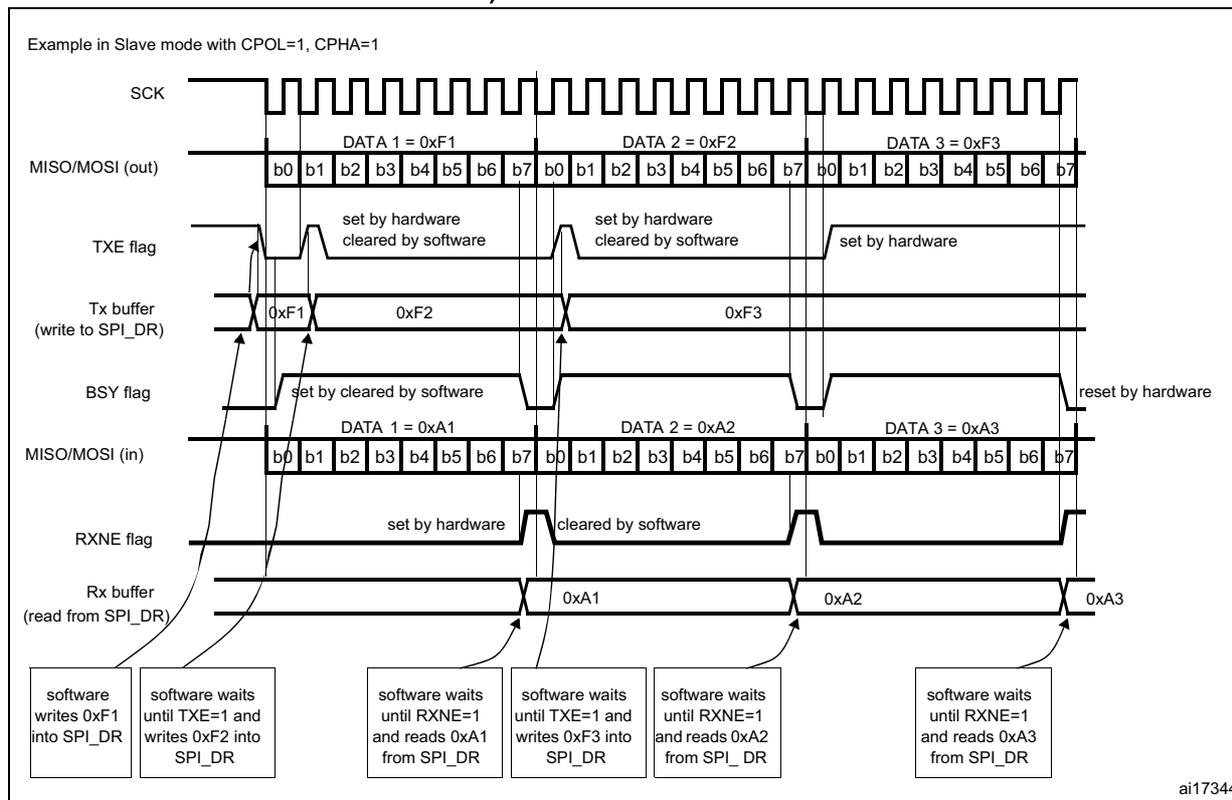
Example in Slave mode with CPOL=1, CPHA=1
The diagram shows the following signals and data over time:
- SCK: Serial clock signal, continuous square wave.
- MISO/MOSI (out): Master In Slave Out / Master Out Slave In (output). It transmits DATA 1 = 0xF1, DATA 2 = 0xF2, and DATA 3 = 0xF3. Each data item is 8 bits (b0 to b7).
- TXE flag: Transmit Buffer Empty flag. It is set by hardware when the Tx buffer is empty and cleared by software when a new data item is written.
- Tx buffer (write to SPI_DR): Contains the data items 0xF1, 0xF2, and 0xF3.
- BSY flag: Busy flag. It is set by hardware when a transfer starts and cleared by software. It is reset by hardware after the last transfer.
- MISO/MOSI (in): Master In Slave Out / Master Out Slave In (input). It receives DATA 1 = 0xA1, DATA 2 = 0xA2, and DATA 3 = 0xA3. Each data item is 8 bits (b0 to b7).
- RXNE flag: Receive Buffer Not Empty flag. It is set by hardware when the Rx buffer contains data and cleared by software when the data is read.
- Rx buffer (read from SPI_DR): Contains the received data items 0xA1, 0xA2, and 0xA3.
Software sequence:
- software writes 0xF1 into SPI_DR
- software waits until TXE=1 and writes 0xF2 into SPI_DR
- software waits until RXNE=1 and reads 0xA1 from SPI_DR
- software waits until TXE=1 and writes 0xF3 into SPI_DR
- software waits until RXNE=1 and reads 0xA2 from SPI_DR
- software waits until RXNE=1 and reads 0xA3 from SPI_DR
ai17344
Transmit-only procedure (BIDIMODE=0 RXONLY=0)
In this mode, the procedure can be reduced as described below and the BSY bit can be used to wait until the completion of the transmission (see Figure 227 and Figure 228).
- 1. Enable the SPI by setting the SPE bit to 1.
- 2. Write the first data item to send into the SPI_DR register (this clears the TXE bit).
- 3. Wait until TXE=1 and write the next data item to be transmitted. Repeat this step for each data item to be transmitted.
- 4. After writing the last data item into the SPI_DR register, wait until TXE=1, then wait until BSY=0, this indicates that the transmission of the last data is complete.
This procedure can be also implemented using dedicated interrupt subroutines launched at each rising edge of the TXE flag.
Note: During discontinuous communications, there is a 2 APB clock period delay between the write operation to SPI_DR and the BSY bit setting. As a consequence, in transmit-only mode, it is mandatory to wait first until TXE is set and then until BSY is cleared after writing the last data.
After transmitting two data items in transmit-only mode, the OVR flag is set in the SPI_SR register since the received data are never read.
Figure 227. TXE/BSY behavior in Master transmit-only mode (BIDIMODE=0 and RXONLY=0) in case of continuous transfers
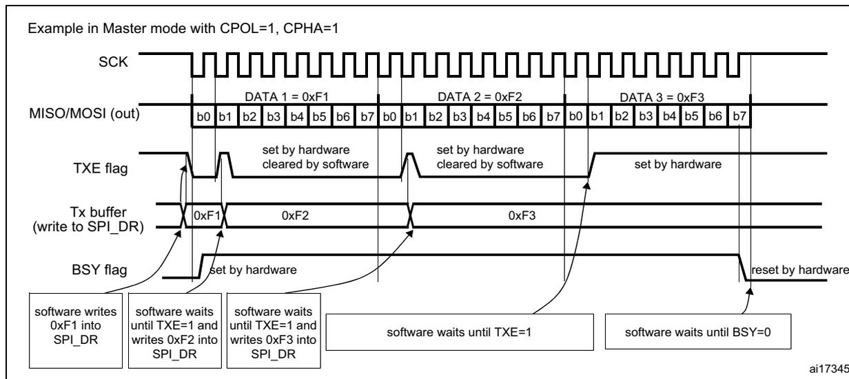
Example in Master mode with CPOL=1, CPHA=1
The diagram illustrates the timing and control signals for a Master transmit-only SPI transfer. The SCK line is a continuous square wave. The MISO/MOSI (out) line shows three 8-bit data transfers: DATA 1 = 0xF1, DATA 2 = 0xF2, and DATA 3 = 0xF3, with bits labeled b0 through b7. The TXE flag is set by hardware when the Tx buffer is empty and cleared by software when the buffer is loaded. The Tx buffer (write to SPI_DR) shows the data values 0xF1, 0xF2, and 0xF3 being written. The BSY flag is set by hardware when the transfer starts and reset by hardware when the transfer is complete. The software sequence is: write 0xF1 into SPI_DR, wait until TXE=1 and write 0xF2 into SPI_DR, wait until TXE=1 and write 0xF3 into SPI_DR, wait until TXE=1, and finally wait until BSY=0.
ai17345
Figure 228. TXE/BSY in Slave transmit-only mode (BIDIMODE=0 and RXONLY=0) in case of continuous transfers
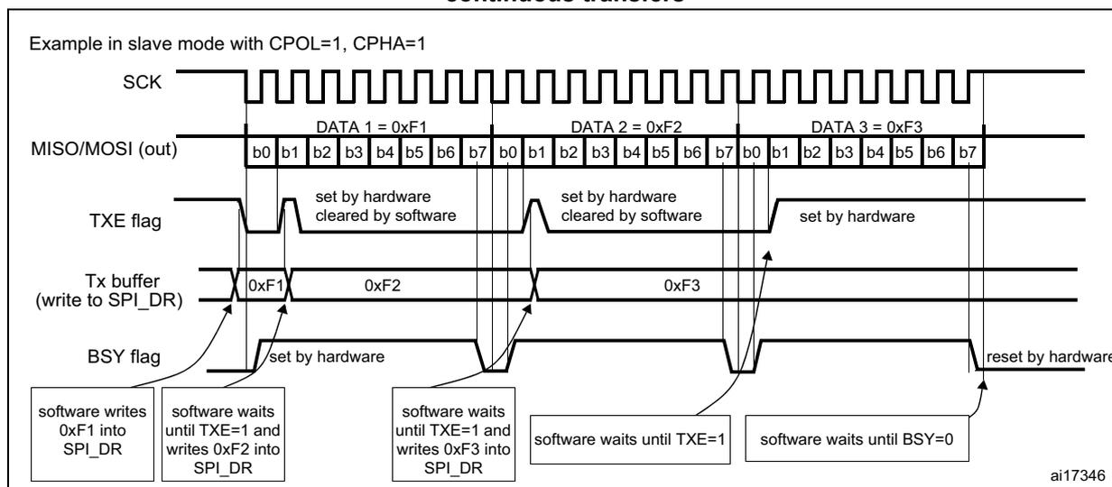
Example in slave mode with CPOL=1, CPHA=1
The diagram illustrates the timing and control signals for a Slave transmit-only SPI transfer. The SCK line is a continuous square wave. The MISO/MOSI (out) line shows three 8-bit data transfers: DATA 1 = 0xF1, DATA 2 = 0xF2, and DATA 3 = 0xF3, with bits labeled b0 through b7. The TXE flag is set by hardware when the Tx buffer is empty and cleared by software when the buffer is loaded. The Tx buffer (write to SPI_DR) shows the data values 0xF1, 0xF2, and 0xF3 being written. The BSY flag is set by hardware when the transfer starts and reset by hardware when the transfer is complete. The software sequence is: write 0xF1 into SPI_DR, wait until TXE=1 and write 0xF2 into SPI_DR, wait until TXE=1 and write 0xF3 into SPI_DR, wait until TXE=1, and finally wait until BSY=0.
ai17346
Bidirectional transmit procedure (BIDIMODE=1 and BIDIOE=1)
In this mode, the procedure is similar to the procedure in Transmit-only mode except that the BIDIMODE and BIDIOE bits both have to be set in the SPI_CR2 register before enabling the SPI.
Unidirectional receive-only procedure (BIDIMODE=0 and RXONLY=1)
In this mode, the procedure can be reduced as described below (see Figure 229 ):
- 1. Set the RXONLY bit in the SPI_CR1 register.
- 2. Enable the SPI by setting the SPE bit to 1:
- a) In master mode, this immediately activates the generation of the SCK clock, and data are serially received until the SPI is disabled (SPE=0).
- b) In slave mode, data are received when the SPI master device drives NSS low and generates the SCK clock.
- 3. Wait until RXNE=1 and read the SPI_DR register to get the received data (this clears the RXNE bit). Repeat this operation for each data item to be received.
This procedure can also be implemented using dedicated interrupt subroutines launched at each rising edge of the RXNE flag.
Note: If it is required to disable the SPI after the last transfer, follow the recommendation described in Section 21.3.8 .
Figure 229. RXNE behavior in receive-only mode (BIDIRMODE=0 and RXONLY=1) in case of continuous transfers
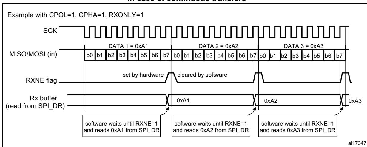
Example with CPOL=1, CPHA=1, RXONLY=1
The diagram illustrates the timing for continuous data transfers in receive-only mode. The SCK line is a continuous square wave. The MISO/MOSI (in) line shows three 8-bit data items: DATA 1 = 0xA1, DATA 2 = 0xA2, and DATA 3 = 0xA3, each consisting of bits b0 through b7. The RXNE flag is shown as a signal that goes high (set by hardware) when a data item is received and goes low (cleared by software) when it is read from the SPI_DR register. The Rx buffer (read from SPI_DR) shows the data items 0xA1, 0xA2, and 0xA3 being read. Below the Rx buffer, three boxes indicate the software procedure: 'software waits until RXNE=1 and reads 0xA1 from SPI_DR', 'software waits until RXNE=1 and reads 0xA2 from SPI_DR', and 'software waits until RXNE=1 and reads 0xA3 from SPI_DR'. The identifier ai17347 is in the bottom right corner.
Bidirectional receive procedure (BIDIMODE=1 and BIDIOE=0)
In this mode, the procedure is similar to the Receive-only mode procedure except that the BIDIMODE bit has to be set and the BIDIOE bit cleared in the SPI_CR2 register before enabling the SPI.
Continuous and discontinuous transfers
When transmitting data in master mode, if the software is fast enough to detect each rising edge of TXE (or TXE interrupt) and to immediately write to the SPI_DR register before the ongoing data transfer is complete, the communication is said to be continuous. In this case, there is no discontinuity in the generation of the SPI clock between each data item and the BSY bit is never cleared between each data transfer.
On the contrary, if the software is not fast enough, this can lead to some discontinuities in the communication. In this case, the BSY bit is cleared between each data transmission (see Figure 230 ).
In Master receive-only mode (RXONLY=1), the communication is always continuous and the BSY flag is always read at 1.
In slave mode, the continuity of the communication is decided by the SPI master device. In any case, even if the communication is continuous, the BSY flag goes low between each transfer for a minimum duration of one SPI clock cycle (see Figure 228).
Figure 230. TXE/BSY behavior when transmitting (BIDIRMODE=0 and RXONLY=0) in case of discontinuous transfers
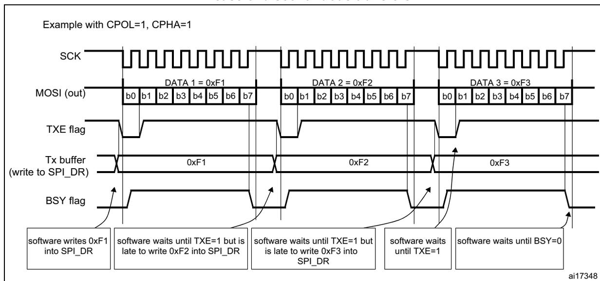
Example with CPOL=1, CPHA=1
The diagram illustrates the timing of SPI transmission for three data bytes: DATA 1 = 0xF1, DATA 2 = 0xF2, and DATA 3 = 0xF3. Each byte is transmitted as 8 bits (b0 to b7). The SCK signal is a continuous square wave. The MOSI (out) signal shows the data bits being transmitted. The TXE flag is high when the Tx buffer is empty and low when it contains data. The BSY flag is high when the transfer is active and low when it is complete. The software writes 0xF1 into SPI_DR, then waits until TXE=1 to write 0xF2, then waits until TXE=1 to write 0xF3, then waits until TXE=1, and finally waits until BSY=0 to start the next transfer.
ai17348
21.3.6 CRC calculation
A CRC calculator has been implemented for communication reliability. Separate CRC calculators are implemented for transmitted data and received data. The CRC is calculated using a programmable polynomial serially on each bit. It is calculated on the sampling clock edge defined by the CPHA and CPOL bits in the SPI_CR1 register.
Note: This SPI offers two kinds of CRC calculation standard which depend directly on the data frame format selected for the transmission and/or reception: 8-bit data (CR8) and 16-bit data (CRC16).
CRC calculation is enabled by setting the CRCEN bit in the SPI_CR1 register. This action resets the CRC registers (SPI_RXCRCR and SPI_TXCRCR). In full duplex or transmitter only mode, when the transfers are managed by the software (CPU mode), it is necessary to write the bit CRCNEXT immediately after the last data to be transferred is written to the SPI_DR. At the end of this last data transfer, the SPI_TXCRCR value is transmitted.
In receive only mode and when the transfers are managed by software (CPU mode), it is necessary to write the CRCNEXT bit after the second last data has been received. The CRC is received just after the last data reception and the CRC check is then performed.
At the end of data and CRC transfers, the CRCERR flag in the SPI_SR register is set if corruption occurs during the transfer.
If data are present in the TX buffer, the CRC value is transmitted only after the transmission of the data byte. During CRC transmission, the CRC calculator is switched off and the register value remains unchanged.
SPI communication using the CRC is possible through the following procedure:
- 1. Program the CPOL, CPHA, LSBFirst, BR, SSM, SSI and MSTR values.
- 2. Program the polynomial in the SPI_CRCPR register.
- 3. Enable the CRC calculation by setting the CRCEN bit in the SPI_CR1 register. This also clears the SPI_RXCRCR and SPI_TXCRCR registers.
- 4. Enable the SPI by setting the SPE bit in the SPI_CR1 register.
- 5. Start the communication and sustain the communication until all but one byte or half-word have been transmitted or received.
- – In full duplex or transmitter-only mode, when the transfers are managed by software, when writing the last byte or half word to the Tx buffer, set the CRCNEXT bit in the SPI_CR1 register to indicate that the CRC is transmitted after the transmission of the last byte.
- – In receiver only mode, set the bit CRCNEXT just after the reception of the second to last data to prepare the SPI to enter in CRC Phase at the end of the reception of the last data. CRC calculation is frozen during the CRC transfer.
- 6. After the transfer of the last byte or half word, the SPI enters the CRC transfer and check phase. In full duplex mode or receiver-only mode, the received CRC is compared to the SPI_RXCRCR value. If the value does not match, the CRCERR flag in SPI_SR is set and an interrupt can be generated when the ERRIE bit in the SPI_CR2 register is set.
Note: When the SPI is in slave mode, be careful to enable CRC calculation only when the clock is stable, that is, when the clock is in the steady state. If not, a wrong CRC calculation may be done. In fact, the CRC is sensitive to the SCK slave input clock as soon as CRCEN is set, and this, whatever the value of the SPE bit.
With high bitrate frequencies, be careful when transmitting the CRC. As the number of used CPU cycles has to be as low as possible in the CRC transfer phase, it is forbidden to call software functions in the CRC transmission sequence to avoid errors in the last data and CRC reception. In fact, CRCNEXT bit has to be written before the end of the transmission/reception of the last data.
For high bit rate frequencies, it is advised to use the DMA mode to avoid the degradation of the SPI speed performance due to CPU accesses impacting the SPI bandwidth.
When the devices are configured as slaves and the NSS hardware mode is used, the NSS pin needs to be kept low between the data phase and the CRC phase.
When the SPI is configured in slave mode with the CRC feature enabled, CRC calculation takes place even if a high level is applied on the NSS pin. This may happen for example in case of a multislave environment where the communication master addresses slaves alternately.
Between a slave deselection (high level on NSS) and a new slave selection (low level on NSS), the CRC value should be cleared on both master and slave sides in order to resynchronize the master and slave for their respective CRC calculation.
To clear the CRC, follow the procedure below:
- 1. Disable SPI (SPE = 0)
- 2. Clear the CRCEN bit
- 3. Set the CRCEN bit
- 4. Enable the SPI (SPE = 1)
21.3.7 Status flags
Four status flags are provided for the application to completely monitor the state of the SPI bus.
Tx buffer empty flag (TXE)
When it is set, this flag indicates that the Tx buffer is empty and the next data to be transmitted can be loaded into the buffer. The TXE flag is cleared when writing to the SPI_DR register.
Rx buffer not empty (RXNE)
When set, this flag indicates that there are valid received data in the Rx buffer. It is cleared when SPI_DR is read.
BUSY flag
This BSY flag is set and cleared by hardware (writing to this flag has no effect). The BSY flag indicates the state of the communication layer of the SPI.
When BSY is set, it indicates that the SPI is busy communicating. There is one exception in master mode / bidirectional receive mode (MSTR=1 and BDM=1 and BDOE=0) where the BSY flag is kept low during reception.
The BSY flag is useful to detect the end of a transfer if the software wants to disable the SPI and enter Halt mode (or disable the peripheral clock). This avoids corrupting the last transfer. For this, the procedure described below must be strictly respected.
The BSY flag is also useful to avoid write collisions in a multimaster system.
The BSY flag is set when a transfer starts, with the exception of master mode / bidirectional receive mode (MSTR=1 and BDM=1 and BDOE=0).
It is cleared:
- • when a transfer is finished (except in master mode if the communication is continuous)
- • when the SPI is disabled
- • when a master mode fault occurs (MODF=1)
When communication is not continuous, the BSY flag is low between each communication.
When communication is continuous:
- • in master mode, the BSY flag is kept high during all the transfers
- • in slave mode, the BSY flag goes low for one SPI clock cycle between each transfer
Note: Do not use the BSY flag to handle each data transmission or reception. It is better to use the TXE and RXNE flags instead.
21.3.8 Disabling the SPI
When a transfer is terminated, the application can stop the communication by disabling the SPI peripheral. This is done by clearing the SPE bit.
For some configurations, disabling the SPI and entering the Halt mode while a transfer is ongoing can cause the current transfer to be corrupted and/or the BSY flag might become unreliable.
To avoid any of those effects, it is recommended to respect the following procedure when disabling the SPI:
In master or slave full-duplex mode (BIDIMODE=0, RXONLY=0)
- 1. Wait until RXNE=1 to receive the last data
- 2. Wait until TXE=1
- 3. Then wait until BSY=0
- 4. Disable the SPI (SPE=0) and, eventually, enter the Halt mode (or disable the peripheral clock)
In master or slave unidirectional transmit-only mode (BIDIMODE=0, RXONLY=0) or bidirectional transmit mode (BIDIMODE=1, BIDIOE=1)
After the last data is written into the SPI_DR register:
- 1. Wait until TXE=1
- 2. Then wait until BSY=0
- 3. Disable the SPI (SPE=0) and, eventually, enter the Halt mode (or disable the peripheral clock)
In master unidirectional receive-only mode (MSTR=1, BIDIMODE=0, RXONLY=1) or bidirectional receive mode (MSTR=1, BIDIMODE=1, BIDIOE=0)
This case must be managed in a particular way to ensure that the SPI does not initiate a new transfer:
- 1. Wait for the second to last occurrence of RXNE=1 (n-1)
- 2. Then wait for one SPI clock cycle (using a software loop) before disabling the SPI (SPE=0)
- 3. Then wait for the last RXNE=1 before entering the Halt mode (or disabling the peripheral clock)
Note: In master bidirectional receive mode (MSTR=1 and BDM=1 and BDOE=0), the BSY flag is kept low during transfers.
In slave receive-only mode (MSTR=0, BIDIMODE=0, RXONLY=1) or bidirectional receive mode (MSTR=0, BIDIMODE=1, BIDIOE=0)
- 1. You can disable the SPI (write SPE=1) at any time: the current transfer completes before the SPI is effectively disabled
- 2. Then, if you want to enter the Halt mode, you must first wait until BSY = 0 before entering the Halt mode (or disabling the peripheral clock).
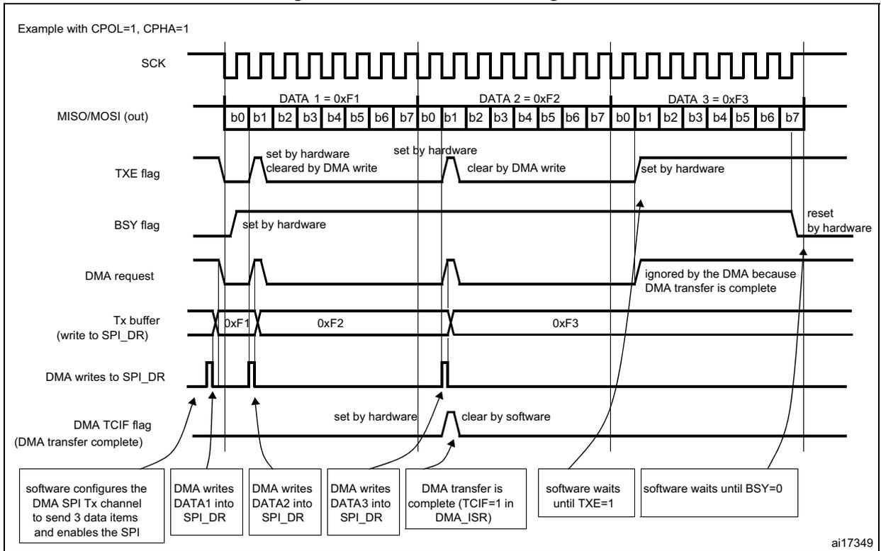
21.3.9 SPI communication using DMA (direct memory addressing)
To operate at its maximum speed, the SPI needs to be fed with the data for transmission and the data received on the Rx buffer should be read to avoid overrun. To facilitate the transfers, the SPI features a DMA capability implementing a simple request/acknowledge protocol.
A DMA access is requested when the enable bit in the SPI_CR2 register is enabled. Separate requests must be issued to the Tx and Rx buffers (see Figure 231 and Figure 232 ):
- • In transmission, a DMA request is issued each time TXE is set to 1. The DMA then writes to the SPI_DR register (this clears the TXE flag).
- • In reception, a DMA request is issued each time RXNE is set to 1. The DMA then reads the SPI_DR register (this clears the RXNE flag).
When the SPI is used only to transmit data, it is possible to enable only the SPI Tx DMA channel. In this case, the OVR flag is set because the data received are not read.
When the SPI is used only to receive data, it is possible to enable only the SPI Rx DMA channel.
In transmission mode, when the DMA has written all the data to be transmitted (flag TCIF is set in the DMA_ISR register), the BSY flag can be monitored to ensure that the SPI communication is complete. This is required to avoid corrupting the last transmission before disabling the SPI or entering the Stop mode. The software must first wait until TXE=1 and then until BSY=0.
Note: During discontinuous communications, there is a 2 APB clock period delay between the write operation to SPI_DR and the BSY bit setting. As a consequence, it is mandatory to wait first until TXE=1 and then until BSY=0 after writing the last data.
Figure 231. Transmission using DMA
Example with CPOL=1, CPHA=1
SCK
MISO/MOSI (out)
DATA 1 = 0xF1
DATA 2 = 0xF2
DATA 3 = 0xF3
TXE flag
BSY flag
DMA request
Tx buffer (write to SPI_DR)
DMA writes to SPI_DR
DMA TCIF flag (DMA transfer complete)
software configures the DMA SPI Tx channel to send 3 data items and enables the SPI
DMA writes DATA1 into SPI_DR
DMA writes DATA2 into SPI_DR
DMA writes DATA3 into SPI_DR
DMA transfer is complete (TCIF=1 in DMA_ISR)
software waits until TXE=1
software waits until BSY=0
ai17349
Figure 232. Reception using DMA
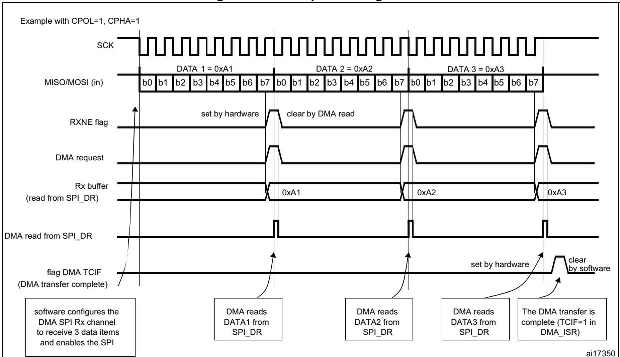
Example with CPOL=1, CPHA=1
SCK
MISO/MOSI (in)
DATA 1 = 0xA1
DATA 2 = 0xA2
DATA 3 = 0xA3
RXNE flag
DMA request
Rx buffer (read from SPI_DR)
DMA read from SPI_DR
DMA TCIF flag (DMA transfer complete)
software configures the DMA SPI Rx channel to receive 3 data items and enables the SPI
DMA reads DATA1 from SPI_DR
DMA reads DATA2 from SPI_DR
DMA reads DATA3 from SPI_DR
The DMA transfer is complete (TCIF=1 in DMA_ISR)
ai17350
DMA capability with CRC
When SPI communication is enabled with CRC communication and DMA mode, the transmission and reception of the CRC at the end of communication are automatic that is without using the bit CRCNEXT. After the CRC reception, the CRC must be read in the SPI_DR register to clear the RXNE flag.
At the end of data and CRC transfers, the CRCERR flag in SPI_SR is set if corruption occurs during the transfer.
21.3.10 Error flags
Master mode fault (MODF)
Master mode fault occurs when the master device has its NSS pin pulled low (in NSS hardware mode) or SSI bit low (in NSS software mode), this automatically sets the MODF bit. Master mode fault affects the SPI peripheral in the following ways:
- • The MODF bit is set and an SPI interrupt is generated if the ERRIE bit is set.
- • The SPE bit is cleared. This blocks all output from the device and disables the SPI interface.
- • The MSTR bit is cleared, thus forcing the device into slave mode.
Use the following software sequence to clear the MODF bit:
- 1. Make a read or write access to the SPI_SR register while the MODF bit is set.
- 2. Then write to the SPI_CR1 register.
To avoid any multiple slave conflicts in a system comprising several MCUs, the NSS pin must be pulled high during the MODF bit clearing sequence. The SPE and MSTR bits can be restored to their original state after this clearing sequence.
As a security, hardware does not allow the setting of the SPE and MSTR bits while the MODF bit is set.
In a slave device the MODF bit cannot be set. However, in a multimaster configuration, the device can be in slave mode with this MODF bit set. In this case, the MODF bit indicates that there might have been a multimaster conflict for system control. An interrupt routine can be used to recover cleanly from this state by performing a reset or returning to a default state.
Overrun condition
An overrun condition occurs when the master device has sent data bytes and the slave device has not cleared the RXNE bit resulting from the previous data byte transmitted.
When an overrun condition occurs:
- • the OVR bit is set and an interrupt is generated if the ERRIE bit is set.
In this case, the receiver buffer contents are not updated with the newly received data from the master device. A read from the SPI_DR register returns this byte. All other subsequently transmitted bytes are lost.
Clearing the OVR bit is done by a read from the SPI_DR register followed by a read access to the SPI_SR register.
CRC errorThis flag is used to verify the validity of the value received when the CRCEN bit in the SPI_CR1 register is set. The CRCERR flag in the SPI_SR register is set if the value received in the shift register does not match the receiver SPI_RXCRCR value.
21.3.11 SPI interrupts Table 119. SPI interrupt requests| Interrupt event | Event flag | Enable Control bit |
|---|---|---|
| Transmit buffer empty flag | TXE | TXEIE |
| Receive buffer not empty flag | RXNE | RXNEIE |
| Master mode fault event | MODF | ERRIE |
| Overrun error | OVR | |
| CRC error flag | CRCERR |
21.4 SPI registers
The peripheral registers have to be accessed by half-words (16 bits) or words (32 bits).
21.4.1 SPI control register 1 (SPI_CR1)
Address offset: 0x00
Reset value: 0x0000
| 15 | 14 | 13 | 12 | 11 | 10 | 9 | 8 | 7 | 6 | 5 | 4 | 3 | 2 | 1 | 0 |
|---|---|---|---|---|---|---|---|---|---|---|---|---|---|---|---|
| BIDI MODE | BIDI OE | CRC EN | CRC NEXT | DFF | RX ONLY | SSM | SSI | LSB FIRST | SPE | BR [2:0] | MSTR | CPOL | CPHA | ||
| rw | rw | rw | rw | rw | rw | rw | rw | rw | rw | rw | rw | rw | rw | rw | rw |
Bit 15 BIDI MODE: Bidirectional data mode enable
0: 2-line unidirectional data mode selected
1: 1-line bidirectional data mode selected
Bit 14 BIDI OE: Output enable in bidirectional mode
This bit combined with the BIDI mode bit selects the direction of transfer in bidirectional mode
0: Output disabled (receive-only mode)
1: Output enabled (transmit-only mode)
Note: In master mode, the MOSI pin is used and in slave mode, the MISO pin is used.
Bit 13 CRCEN: Hardware CRC calculation enable
0: CRC calculation disabled
1: CRC calculation Enabled
Note: This bit should be written only when SPI is disabled (SPE = '0') for correct operation
Bit 12 CRCNEXT: CRC transfer next
0: Data phase (no CRC phase)
1: Next transfer is CRC (CRC phase)
Note: When the SPI is configured in full duplex or transmitter only modes, CRCNEXT must be written as soon as the last data is written to the SPI_DR register.
When the SPI is configured in receiver only mode, CRCNEXT must be set after the second last data reception.
This bit should be kept cleared when the transfers are managed by DMA.
Bit 11 DFF: Data frame format
0: 8-bit data frame format is selected for transmission/reception
1: 16-bit data frame format is selected for transmission/reception
Note: This bit should be written only when SPI is disabled (SPE = '0') for correct operation
Bit 10 RXONLY: Receive only
This bit combined with the BIDI mode bit selects the direction of transfer in 2-line unidirectional mode. This bit is also useful in a multislave system in which this particular slave is not accessed, the output from the accessed slave is not corrupted.
0: Full duplex (Transmit and receive)
1: Output disabled (Receive-only mode)
Bit 9 SSM: Software slave management
When the SSM bit is set, the NSS pin input is replaced with the value from the SSI bit.
0: Software slave management disabled
1: Software slave management enabled
Bit 8 SSI: Internal slave select
This bit has an effect only when the SSM bit is set. The value of this bit is forced onto the NSS pin and the IO value of the NSS pin is ignored.
Bit 7 LSBFIRST: Frame format
0: MSB transmitted first
1: LSB transmitted first
Note: This bit should not be changed when communication is ongoing.
Bit 6 SPE: SPI enable
0: Peripheral disabled
1: Peripheral enabled
Note: When disabling the SPI, follow the procedure described in Section 21.3.8: Disabling the SPI .
Bits 5:3 BR[2:0]: Baud rate control
000: \( f_{PCLK}/2 \)
001: \( f_{PCLK}/4 \)
010: \( f_{PCLK}/8 \)
011: \( f_{PCLK}/16 \)
100: \( f_{PCLK}/32 \)
101: \( f_{PCLK}/64 \)
110: \( f_{PCLK}/128 \)
111: \( f_{PCLK}/256 \)
Note: These bits should not be changed when communication is ongoing.
Bit 2 MSTR: Master selection
0: Slave configuration
1: Master configuration
Note: This bit should not be changed when communication is ongoing.
Bit 1 CPOL: Clock polarity
0: CK to 0 when idle
1: CK to 1 when idle
Note: This bit should not be changed when communication is ongoing.
Bit 0 CPHA: Clock phase
0: The first clock transition is the first data capture edge
1: The second clock transition is the first data capture edge
Note: This bit should not be changed when communication is ongoing.
21.4.2 SPI control register 2 (SPI_CR2)
Address offset: 0x04
Reset value: 0x0000
| 15 | 14 | 13 | 12 | 11 | 10 | 9 | 8 | 7 | 6 | 5 | 4 | 3 | 2 | 1 | 0 |
|---|---|---|---|---|---|---|---|---|---|---|---|---|---|---|---|
| Reserved | TXEIE | RXNEIE | ERRIE | Res. | Res. | SSOE | TXDMAEN | RXDMAEN | |||||||
| rw | rw | rw | rw | rw | rw | ||||||||||
Bits 15:8 Reserved, must be kept at reset value.
Bit 7 TXEIE : Tx buffer empty interrupt enable
0: TXE interrupt masked
1: TXE interrupt not masked. Used to generate an interrupt request when the TXE flag is set.
Bit 6 RXNEIE : RX buffer not empty interrupt enable
0: RXNE interrupt masked
1: RXNE interrupt not masked. Used to generate an interrupt request when the RXNE flag is set.
Bit 5 ERRIE : Error interrupt enable
This bit controls the generation of an interrupt when an error condition occurs ).
0: Error interrupt is masked
1: Error interrupt is enabled
Bits 4:3 Reserved, must be kept at reset value.
Bit 2 SSOE : SS output enable
0: SS output is disabled in master mode and the cell can work in multimaster configuration
1: SS output is enabled in master mode and when the cell is enabled. The cell cannot work in a multimaster environment.
Bit 1 TXDMAEN : Tx buffer DMA enable
When this bit is set, the DMA request is made whenever the TXE flag is set.
0: Tx buffer DMA disabled
1: Tx buffer DMA enabled
Bit 0 RXDMAEN : Rx buffer DMA enable
When this bit is set, the DMA request is made whenever the RXNE flag is set.
0: Rx buffer DMA disabled
1: Rx buffer DMA enabled
21.4.3 SPI status register (SPI_SR)
Address offset: 0x08
Reset value: 0x0002
| 15 | 14 | 13 | 12 | 11 | 10 | 9 | 8 | 7 | 6 | 5 | 4 | 3 | 2 | 1 | 0 |
|---|---|---|---|---|---|---|---|---|---|---|---|---|---|---|---|
| Reserved | BSY | OVR | MODF | CRC ERR | Reserved | TXE | RXNE | ||||||||
| r | r | r | rc_w0 | r | r | ||||||||||
Bits 15:8 Reserved, must be kept at reset value.
Bit 7 BSY : Busy flag
0: SPI not busy
1: SPI is busy in communication or Tx buffer is not empty
This flag is set and cleared by hardware.
Note: BSY flag must be used with caution: refer to Section 21.3.7 and Section 21.3.8 .
Bit 6 OVR : Overrun flag
0: No overrun occurred
1: Overrun occurred
This flag is set by hardware and reset by a software sequence.
Bit 5 MODF : Mode fault0: No mode fault occurred
1: Mode fault occurred
This flag is set by hardware and reset by a software sequence. Refer to Section 21.3.10 on page 557 for the software sequence.Bit 4 CRCERR : CRC error flag0: CRC value received matches the SPI_RXCRCR value
1: CRC value received does not match the SPI_RXCRCR value
This flag is set by hardware and cleared by software writing 0.
Bits 3:2 Reserved
Bit 1 TXE : Transmit buffer empty0: Tx buffer not empty
1: Tx buffer empty
Bit 0 RXNE : Receive buffer not empty0: Rx buffer empty
1: Rx buffer not empty
21.4.4 SPI data register (SPI_DR)Address offset: 0x0C
Reset value: 0x0000

| 15 | 14 | 13 | 12 | 11 | 10 | 9 | 8 | 7 | 6 | 5 | 4 | 3 | 2 | 1 | 0 |
|---|---|---|---|---|---|---|---|---|---|---|---|---|---|---|---|
| DR[15:0] | |||||||||||||||
| rw | rw | rw | rw | rw | rw | rw | rw | rw | rw | rw | rw | rw | rw | rw | rw |
Data received or to be transmitted.
The data register is split into 2 buffers - one for writing (Transmit Buffer) and another one for reading (Receive buffer). A write to the data register writes into the Tx buffer and a read from the data register returns the value held in the Rx buffer.
Note: These notes apply to SPI mode: Depending on the data frame format selection bit (DFF in SPI_CR1 register), the data sent or received is either 8-bit or 16-bit. This selection has to be made before enabling the SPI to ensure correct operation. For an 8-bit data frame, the buffers are 8-bit and only the LSB of the register (SPI_DR[7:0]) is used for transmission/reception. When in reception mode, the MSB of the register (SPI_DR[15:8]) is forced to 0. For a 16-bit data frame, the buffers are 16-bit and the entire register, SPI_DR[15:0] is used for transmission/reception.21.4.5 SPI CRC polynomial register (SPI_CRCPR)
Address offset: 0x10
Reset value: 0x0007

| 15 | 14 | 13 | 12 | 11 | 10 | 9 | 8 | 7 | 6 | 5 | 4 | 3 | 2 | 1 | 0 |
|---|---|---|---|---|---|---|---|---|---|---|---|---|---|---|---|
| CRCPOLY[15:0] | |||||||||||||||
| rw | rw | rw | rw | rw | rw | rw | rw | rw | rw | rw | rw | rw | rw | rw | rw |
Bits 15:0 CRCPOLY[15:0] : CRC polynomial register
This register contains the polynomial for the CRC calculation.
The CRC polynomial (0007h) is the reset value of this register. Another polynomial can be configured as required.
21.4.6 SPI RX CRC register (SPI_RXCRCR)
Address offset: 0x14
Reset value: 0x0000

| 15 | 14 | 13 | 12 | 11 | 10 | 9 | 8 | 7 | 6 | 5 | 4 | 3 | 2 | 1 | 0 |
|---|---|---|---|---|---|---|---|---|---|---|---|---|---|---|---|
| RXCRC[15:0] | |||||||||||||||
| r | r | r | r | r | r | r | r | r | r | r | r | r | r | r | r |
Bits 15:0 RXCRC[15:0] : Rx CRC register
When CRC calculation is enabled, the RxCRC[15:0] bits contain the computed CRC value of the subsequently received bytes. This register is reset when the CRCEN bit in SPI_CR1 register is written to 1. The CRC is calculated serially using the polynomial programmed in the SPI_CRCPR register.
Only the 8 LSB bits are considered when the data frame format is set to be 8-bit data (DFF bit of SPI_CR1 is cleared). CRC calculation is done based on any CRC8 standard.
The entire 16-bits of this register are considered when a 16-bit data frame format is selected (DFF bit of the SPI_CR1 register is set). CRC calculation is done based on any CRC16 standard.
Note: A read to this register when the BSY Flag is set could return an incorrect value.
21.4.7 SPI TX CRC register (SPI_TXCRCR)
Address offset: 0x18
Reset value: 0x0000
| 15 | 14 | 13 | 12 | 11 | 10 | 9 | 8 | 7 | 6 | 5 | 4 | 3 | 2 | 1 | 0 |
|---|---|---|---|---|---|---|---|---|---|---|---|---|---|---|---|
| TXCRC[15:0] | |||||||||||||||
| r | r | r | r | r | r | r | r | r | r | r | r | r | r | r | r |
Bits 15:0 TXCRC[15:0] : Tx CRC register
When CRC calculation is enabled, the TxCRC[7:0] bits contain the computed CRC value of the subsequently transmitted bytes. This register is reset when the CRCEN bit of SPI_CR1 is written to 1. The CRC is calculated serially using the polynomial programmed in the SPI_CRCPR register.
Only the 8 LSB bits are considered when the data frame format is set to be 8-bit data (DFF bit of SPI_CR1 is cleared). CRC calculation is done based on any CRC8 standard.
The entire 16-bits of this register are considered when a 16-bit data frame format is selected (DFF bit of the SPI_CR1 register is set). CRC calculation is done based on any CRC16 standard.
Note: A read to this register when the BSY flag is set could return an incorrect value.
21.4.8 SPI register map
The table provides shows the SPI register map and reset values.
Table 120. SPI register map and reset values
| Offset | Register | 31 | 30 | 29 | 28 | 27 | 26 | 25 | 24 | 23 | 22 | 21 | 20 | 19 | 18 | 17 | 16 | 15 | 14 | 13 | 12 | 11 | 10 | 9 | 8 | 7 | 6 | 5 | 4 | 3 | 2 | 1 | 0 |
|---|---|---|---|---|---|---|---|---|---|---|---|---|---|---|---|---|---|---|---|---|---|---|---|---|---|---|---|---|---|---|---|---|---|
| 0x00 | SPI_CR1 | Reserved | BIDIMODE | BIDIOE | CRCEN | CRCNEXT | DFF | RXONLY | SSM | SSI | LSBFIRST | SPE | BR [2:0] | MSTR | CPOL | CPHA | |||||||||||||||||
| Reset value | 0 | 0 | 0 | 0 | 0 | 0 | 0 | 0 | 0 | 0 | 0 | 0 | 0 | 0 | 0 | 0 | |||||||||||||||||
| 0x04 | SPI_CR2 | Reserved | TXEIE | RXNEIE | ERRIE | Reserved | SSOE | TXDMAEN | RXDMAEN | ||||||||||||||||||||||||
| Reset value | 0 | 0 | 0 | 0 | 0 | 0 | |||||||||||||||||||||||||||
| 0x08 | SPI_SR | Reserved | BSY | OVR | MODF | CRCERR | Reserved | TXE | RXNE | ||||||||||||||||||||||||
| Reset value | 0 | 0 | 0 | 0 | -1 | 0 | |||||||||||||||||||||||||||
| 0x0C | SPI_DR | Reserved | DR[15:0] | ||||||||||||||||||||||||||||||
| Reset value | 0 | 0 | 0 | 0 | 0 | 0 | 0 | 0 | 0 | 0 | 0 | 0 | 0 | 0 | 0 | 0 | |||||||||||||||||
| 0x10 | SPI_CRCPR | Reserved | CRCPOLY[15:0] | ||||||||||||||||||||||||||||||
| Reset value | 0 | 0 | 0 | 0 | 0 | 0 | 0 | 0 | 0 | 0 | 0 | 0 | 0 | 1 | 1 | 1 | |||||||||||||||||
| 0x14 | SPI_RXCRCR | Reserved | RxCRC[15:0] | ||||||||||||||||||||||||||||||
| Reset value | 0 | 0 | 0 | 0 | 0 | 0 | 0 | 0 | 0 | 0 | 0 | 0 | 0 | 0 | 0 | 0 | |||||||||||||||||
| 0x18 | SPI_TXCRCR | Reserved | TxCRC[15:0] | ||||||||||||||||||||||||||||||
| Reset value | 0 | 0 | 0 | 0 | 0 | 0 | 0 | 0 | 0 | 0 | 0 | 0 | 0 | 0 | 0 | 0 | |||||||||||||||||
Refer to Section 3.3: Memory map for the register boundary addresses.