20. Flexible static memory controller (FSMC)
Low-density value line devices are STM32F100xx microcontrollers where the flash memory density ranges between 16 and 32 Kbytes.
Medium-density value line devices are STM32F100xx microcontrollers where the flash memory density ranges between 64 and 128 Kbytes.
High-density value line devices are STM32F100xx microcontrollers where the flash memory density ranges between 256 and 512 Kbytes.
This section applies to high-density value line devices only.
20.1 FSMC main features
The FSMC block is able to interface with synchronous and asynchronous memories. Its main purpose is to:
- • Translate the AHB transactions into the appropriate external device protocol
- • Meet the access timing requirements of the external devices
All external memories share the addresses, data and control signals with the controller. Each external device is accessed by means of a unique chip select. The FSMC performs only one access at a time to an external device.
The FSMC has the following main features:
- • Interfaces with static memory-mapped devices including:
- – Static random access memory (SRAM)
- – NOR/OneNAND flash memory
- – PSRAM (4 memory banks)
- • Supports burst mode access to synchronous devices (NOR flash and PSRAM)
- • 8- or 16-bit wide databus
- • Independent chip select control for each memory bank
- • Independent configuration for each memory bank
- • Programmable timings to support a wide range of devices, in particular:
- – Programmable wait states (up to 15)
- – Programmable bus turnaround cycles (up to 15)
- – Programmable output enable and write enable delays (up to 15)
- – Independent read and write timings and protocol, so as to support the widest variety of memories and timings
- • Write enable and byte lane select outputs for use with PSRAM and SRAM devices
- • Translation of 32-bit wide AHB transactions into consecutive 16-bit or 8-bit accesses to external 16-bit or 8-bit devices
- • A Write FIFO, 2-word long, each word is 32 bits wide, only stores data and not the address. Therefore, this FIFO only buffers AHB write burst transactions. This makes it possible to write to slow memories and free the AHB quickly for other operations. Only one burst at a time is buffered: if a new AHB burst or single transaction occurs while an
operation is in progress, the FIFO is drained. The FSMC inserts wait states until the current memory access is complete.
- • External asynchronous wait control
The FSMC registers that define the external device type and associated characteristics are usually set at boot time and do not change until the next reset or power-up. However, it is possible to change the settings at any time.
20.2 Block diagram
The FSMC consists of four main blocks:
- • The AHB interface (including the FSMC configuration registers)
- • The NOR flash/PSRAM controller
- • The external device interface
The block diagram is shown in Figure 202 .
![Figure 202. FSMC block diagram. The diagram shows the internal structure of the FSMC. On the left, an 'AHB bus' is connected to a 'Configuration registers' block and a 'NOR/PSRAM memory controller' block. Above the FSMC, an 'FSMC interrupt to NVIC' is shown. To the right, a list of signals is shown, grouped by a bracket as 'NOR/PSRAM signals': FSMC_NE[4:1], FSMC_NL (or NADV), FSMC_NBL[1:0], FSMC_CLK, FSMC_A[25:0], FSMC_D[15:0], FSMC_NOE, FSMC_NWE, and FSMC_NWAIT. The signal FSMC_NL (or NADV) is also labeled as 'From clock controller' and 'HCLK'. The diagram is labeled 'ai18305b' in the bottom right corner.](/RM0041-STM32F100/022c3fe03367d9ff32c51f3c52ef7de5_img.jpg)
Figure 202. FSMC block diagram
20.3 AHB interface
The AHB slave interface enables internal CPUs and other bus master peripherals to access the external static memories.
AHB transactions are translated into the external device protocol. In particular, if the selected external memory is 16 or 8 bits wide, 32-bit wide transactions on the AHB are split into consecutive 16- or 8-bit accesses. The FSMC Chip Select (FSMC_NEx) does not toggle between consecutive accesses except when performing accesses in mode D with the extended mode enabled.
The FSMC generates an AHB error in the following conditions:
- • When reading or writing to an FSMC bank which is not enabled
- • When reading or writing to the NOR flash bank while the FACCEN bit is reset in the FSMC_BCRx register.
The effect of this AHB error depends on the AHB master which has attempted the R/W access:
- • If it is the Cortex®-M3 CPU, a hard fault interrupt is generated
- • If is a DMA, a DMA transfer error is generated and the corresponding DMA channel is automatically disabled.
The AHB clock (HCLK) is the reference clock for the FSMC.
20.3.1 Supported memories and transactions
General transaction rules
The requested AHB transaction data size can be 8-, 16- or 32-bit wide whereas the accessed external device has a fixed data width. This may lead to inconsistent transfers.
Therefore, some simple transaction rules must be followed:
- • AHB transaction size and memory data size are equal
There is no issue in this case. - • AHB transaction size is greater than the memory size
In this case, the FSMC splits the AHB transaction into smaller consecutive memory accesses in order to meet the external data width. - • AHB transaction size is smaller than the memory size
Asynchronous transfers may or not be consistent depending on the type of external device.- – Asynchronous accesses to devices that have the byte select feature (SRAM, ROM, PSRAM).
- a) FSMC allows write transactions accessing the right data through its byte lanes NBL[1:0]
- b) Read transactions are allowed. All memory bytes are read and the useless ones are discarded. The NBL[1:0] are kept low during read transactions.
- – Asynchronous accesses to devices that do not have the byte select feature (NOR ).
This situation occurs when a byte access is requested to a 16-bit wide flash memory. Clearly, the device cannot be accessed in byte mode (only 16-bit words can be read from/written to the flash memory) therefore:- a) Write transactions are not allowed
- b) Read transactions are allowed. All memory bytes are read and the useless ones are discarded. The NBL[1:0] are set to 0 during read transactions.
- – Asynchronous accesses to devices that have the byte select feature (SRAM, ROM, PSRAM).
Configuration registers
The FSMC can be configured using a register set. See Section 20.5.6 , for a detailed description of the NOR flash/PSRAM control registers.
20.4 External device address mapping
From the FSMC point of view, the external memory is composed of a single fixed size bank of 256 Mbytes (Refer to Figure 203 ):
- • Bank 1 used to address up to four NOR flash or PSRAM memory devices. This bank is split into 4 NOR/PSRAM subbanks with four dedicated chip selects, as follows:
- – Bank 1 - NOR/PSRAM 1
- – Bank 1 - NOR/PSRAM 2
- – Bank 1 - NOR/PSRAM 3
- – Bank 1 - NOR/PSRAM 4
For each bank the type of memory to be used is user-defined in the Configuration register.
Figure 203. FSMC memory banks
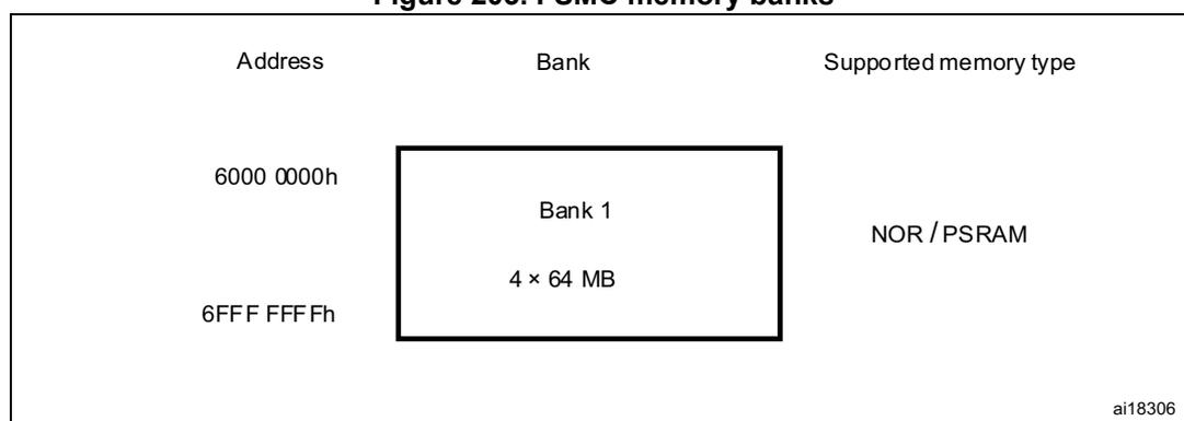
The diagram illustrates the memory bank structure. It shows an address range from 6000 0000h to 6FFF FFF Fh. A central box represents 'Bank 1', which is further divided into '4 x 64 MB' subbanks. To the right, the 'Supported memory type' is listed as 'NOR / PSRAM'. A small code 'ai18306' is visible in the bottom right corner.
20.4.1 NOR/PSRAM address mapping
HADDR[27:26] bits are used to select one of the four memory banks as shown in Table 90 .
Table 90. NOR/PSRAM bank selection
| HADDR[27:26] (1) | Selected bank |
|---|---|
| 00 | Bank 1 - NOR/PSRAM 1 |
| 01 | Bank 1 - NOR/PSRAM 2 |
| 10 | Bank 1 - NOR/PSRAM 3 |
| 11 | Bank 1 - NOR/PSRAM 4 |
1. HADDR are internal AHB address lines that are translated to external memory.
HADDR[25:0] contain the external memory address. Since HADDR is a byte address whereas the memory is addressed in words, the address actually issued to the memory varies according to the memory data width, as shown in the following table.
Table 91. External memory address
| Memory width (1) | Data address issued to the memory | Maximum memory capacity (bits) |
|---|---|---|
| 8-bit | HADDR[25:0] | 64 Mbyte x 8 = 512 Mbit |
| 16-bit | HADDR[25:1] >> 1 | 64 Mbyte/2 x 16 = 512 Mbit |
- 1. In case of a 16-bit external memory width, the FSMC internally uses HADDR[25:1] to generate the address for external memory FSMC_A[24:0]. Whatever the external memory width (16-bit or 8-bit), FSMC_A[0] should be connected to external memory address A[0].
Wrap support for NOR flash/PSRAM
Wrap burst mode for synchronous memories is not supported. The memories must be configured in linear burst mode of undefined length.
20.5 NOR flash/PSRAM controller
The FSMC generates the appropriate signal timings to drive the following types of memories:
- • Asynchronous SRAM and ROM
- – 8-bit
- – 16-bit
- – 32-bit
- • PSRAM (Cellular RAM)
- – Asynchronous mode
- – Burst mode for synchronous accesses
- • NOR flash
- – Asynchronous mode
- – Burst mode for synchronous accesses
- – Multiplexed or nonmultiplexed
The FSMC outputs a unique chip select signal NE[4:1] per bank. All the other signals (addresses, data and control) are shared.
For synchronous accesses, the FSMC issues the clock (CLK) to the selected external device only during the read/write transactions. This clock is a submultiple of the HCLK clock. The size of each bank is fixed and equal to 64 Mbytes.
Each bank is configured by means of dedicated registers (see Section 20.5.6 ).
The programmable memory parameters include access timings (see Table 92 ) and support for wait management (for PSRAM and NOR flash accessed in burst mode).
Table 92. Programmable NOR/PSRAM access parameters
| Parameter | Function | Access mode | Unit | Min. | Max. |
|---|---|---|---|---|---|
| Address setup | Duration of the address setup phase | Asynchronous | AHB clock cycle (HCLK) | 0 | 15 |
| Address hold | Duration of the address hold phase | Asynchronous, muxed I/Os | AHB clock cycle (HCLK) | 1 | 15 |
| Data setup | Duration of the data setup phase | Asynchronous | AHB clock cycle (HCLK) | 1 | 256 |
| Bus turn | Duration of the bus turnaround phase | Asynchronous and synchronous read/write | AHB clock cycle (HCLK) | 0 | 15 |
| Parameter | Function | Access mode | Unit | Min. | Max. |
|---|---|---|---|---|---|
| Clock divide ratio | Number of AHB clock cycles (HCLK) to build one memory clock cycle (CLK) | Synchronous | AHB clock cycle (HCLK) | 2 | 16 |
| Data latency | Number of clock cycles to issue to the memory before the first data of the burst | Synchronous | Memory clock cycle (CLK) | 2 | 17 |
20.5.1 External memory interface signals
Table 93 , Table 94 and Table 95 list the signals that are typically used to interface NOR flash, SRAM and PSRAM.
Note: Prefix “N”. specifies the associated signal as active low.
NOR flash, nonmultiplexed I/Os
Table 93. Nonmultiplexed I/O NOR flash| FSMC signal name | I/O | Function |
|---|---|---|
| CLK | O | Clock (for synchronous access) |
| A[25:0] | O | Address bus |
| D[15:0] | I/O | Bidirectional data bus |
| NE[x] | O | Chip select, x = 1..4 |
| NOE | O | Output enable |
| NWE | O | Write enable |
| NL(=NADV) | O | Latch enable (this signal is called address valid, NADV, by some NOR flash devices) |
| NWAIT | I | NOR flash wait input signal to the FSMC |
NOR flash memories are addressed in 16-bit words. The maximum capacity is 512 Mbit (26 address lines).
NOR flash, multiplexed I/Os
Table 94. Multiplexed I/O NOR flash| FSMC signal name | I/O | Function |
|---|---|---|
| CLK | O | Clock (for synchronous access) |
| A[25:16] | O | Address bus |
| AD[15:0] | I/O | 16-bit multiplexed, bidirectional address/data bus |
| NE[x] | O | Chip select, x = 1..4 |
| NOE | O | Output enable |
| NWE | O | Write enable |
| FSMC signal name | I/O | Function |
|---|---|---|
| NL(=NADV) | O | Latch enable (this signal is called address valid, NADV, by some NOR flash devices) |
| NWAIT | I | NOR flash wait input signal to the FSMC |
NOR-flash memories are addressed in 16-bit words. The maximum capacity is 512 Mbit (26 address lines).
PSRAM/SRAM, nonmultiplexed I/Os
Table 95. Nonmultiplexed I/Os PSRAM/SRAM| FSMC signal name | I/O | Function |
|---|---|---|
| CLK | O | Clock (only for PSRAM synchronous access) |
| A[25:0] | O | Address bus |
| D[15:0] | I/O | Data bidirectional bus |
| NE[x] | O | Chip select, x = 1..4 (called NCE by PSRAM (Cellular RAM i.e. CDRAM)) |
| NOE | O | Output enable |
| NWE | O | Write enable |
| NL(= NADV) | O | Address valid only for PSRAM input (memory signal name: NADV) |
| NWAIT | I | PSRAM wait input signal to the FSMC |
| NBL[1] | O | Upper byte enable (memory signal name: NUB) |
| NBL[0] | O | Lowed byte enable (memory signal name: NLB) |
PSRAM memories are addressed in 16-bit words. The maximum capacity is 512 Mbit (26 address lines).
PSRAM, multiplexed I/Os
Table 96. Multiplexed I/O PSRAM| FSMC signal name | I/O | Function |
|---|---|---|
| CLK | O | Clock (for synchronous access) |
| A[25:16] | O | Address bus |
| AD[15:0] | I/O | 16-bit multiplexed, bidirectional address/data bus |
| NE[x] | O | Chip select, x = 1..4 (called NCE by PSRAM (Cellular RAM i.e. CDRAM)) |
| NOE | O | Output enable |
| NWE | O | Write enable |
| NL(= NADV) | O | Address valid PSRAM input (memory signal name: NADV) |
| NWAIT | I | PSRAM wait input signal to the FSMC |
Table 96. Multiplexed I/O PSRAM (continued)
| FSMC signal name | I/O | Function |
|---|---|---|
| NBL[1] | O | Upper byte enable (memory signal name: NUB) |
| NBL[0] | O | Lowed byte enable (memory signal name: NLB) |
PSRAM memories are addressed in 16-bit words. The maximum capacity is 512 Mbit (26 address lines).
20.5.2 Supported memories and transactions
Table 97 below displays an example of the supported devices, access modes and transactions when the memory data bus is 16-bit for NOR, PSRAM and SRAM. Transactions not allowed (or not supported) by the FSMC in this example appear in gray.
Table 97. NOR flash/PSRAM controller: example of supported memories and transactions
| Device | Mode | R/W | AHB data size | Memory data size | Allowed/not allowed | Comments |
|---|---|---|---|---|---|---|
| NOR flash (muxed I/Os and nonmuxed I/Os) | Asynchronous | R | 8 | 16 | Y | - |
| Asynchronous | W | 8 | 16 | N | - | |
| Asynchronous | R | 16 | 16 | Y | - | |
| Asynchronous | W | 16 | 16 | Y | - | |
| Asynchronous | R | 32 | 16 | Y | Split into two FSMC accesses | |
| Asynchronous | W | 32 | 16 | Y | Split into two FSMC accesses | |
| Asynchronous page | R | - | 16 | N | Mode is not supported | |
| Synchronous | R | 8 | 16 | N | - | |
| Synchronous | R | 16 | 16 | Y | - | |
| Synchronous | R | 32 | 16 | Y | - | |
| PSRAM (multiplexed and nonmultiplexed I/Os) | Asynchronous | R | 8 | 16 | Y | - |
| Asynchronous | W | 8 | 16 | Y | Use of byte lanes NBL[1:0] | |
| Asynchronous | R | 16 | 16 | Y | - | |
| Asynchronous | W | 16 | 16 | Y | - | |
| Asynchronous | R | 32 | 16 | Y | Split into two FSMC accesses | |
| Asynchronous | W | 32 | 16 | Y | Split into two FSMC accesses | |
| Asynchronous page | R | - | 16 | N | Mode is not supported | |
| Synchronous | R | 8 | 16 | N | - | |
| Synchronous | R | 16 | 16 | Y | - | |
| Synchronous | R | 32 | 16 | Y | - | |
| Synchronous | W | 8 | 16 | Y | Use of byte lanes NBL[1:0] | |
| Synchronous | W | 16 / 32 | 16 | Y | - |
Table 97. NOR flash/PSRAM controller: example of supported memories and transactions
| Device | Mode | R/W | AHB data size | Memory data size | Allowed/not allowed | Comments |
|---|---|---|---|---|---|---|
| SRAM and ROM | Asynchronous | R | 8 / 16 | 16 | Y | - |
| Asynchronous | W | 8 / 16 | 16 | Y | Use of byte lanes NBL[1:0] | |
| Asynchronous | R | 32 | 16 | Y | Split into two FSMC accesses | |
| Asynchronous | W | 32 | 16 | Y | Split into two FSMC accesses. Use of byte lanes NBL[1:0] |
20.5.3 General timing rules
Signals synchronization
- All controller output signals change on the rising edge of the internal clock (HCLK)
- In synchronous mode (read or write), all output signals change on the rising edge of HCLK. Whatever the CLKDIV value, all outputs change as follows:
- NOEL/NWEL/ NEL/NADVL/ NADVH /NBLL/ Address valid outputs change on the falling edge of FSMC_CLK clock.
- NOEH/ NWEH / NEH/ NOEH/NBLH/ Address invalid outputs change on the rising edge of FSMC_CLK clock.
20.5.4 NOR flash/PSRAM controller asynchronous transactions
Asynchronous static memories (NOR flash memory, PSRAM, SRAM)
- Signals are synchronized by the internal clock HCLK. This clock is not issued to the memory
- The FSMC always samples the data before de-asserting the NOE signals. This guarantees that the memory data-hold timing constraint is met (chip enable high to data transition, usually 0 ns min.)
- If the extended mode is enabled (EXTMOD bit is set in the FSMC_BCRx register), up to four extended modes (A, B, C and D) are available. It is possible to mix A, B, C and D modes for read and write operations. For example, read operation can be performed in mode A and write in mode B.
- If the extended mode is disabled (EXTMOD bit is reset in the FSMC_BCRx register), the FSMC can operate in Mode1 or Mode2 as follows:
- Mode 1 is the default mode when SRAM/PSRAM memory type is selected (MTYP[0:1] = 0x0 or 0x01 in the FSMC_BCRx register)
- Mode 2 is the default mode when NOR memory type is selected (MTYP[0:1] = 0x10 in the FSMC_BCRx register).
Mode 1 - SRAM/PSRAM (CRAM)
The next figures show the read and write transactions for the supported modes followed by the required configuration of FSMC_BCRx, and FSMC_BTRx/FSMC_BWTRx registers.
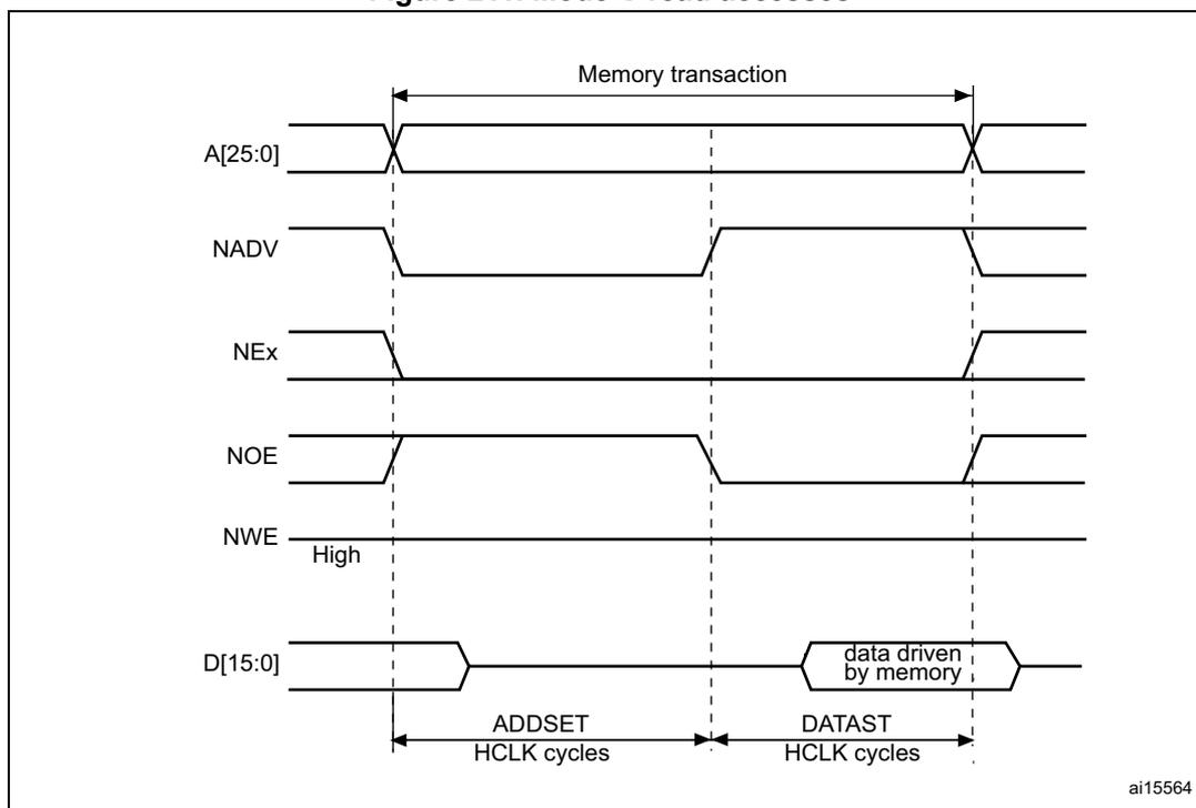
Figure 204. Mode1 read accesses
![Timing diagram for Mode1 read accesses showing signals A[25:0], NBL[1:0], NEx, NOE, NWE, and D[15:0] over time. The diagram shows a memory transaction starting with address and control signals, followed by data being driven by memory. ADDSET and DATAST are measured in HCLK cycles.](/RM0041-STM32F100/7df58b21318b6c6c5477059b5cdbecc8_img.jpg)
The diagram illustrates the timing for a Mode1 read access. The signals shown are:
- A[25:0] : Address bus, valid during the memory transaction.
- NBL[1:0] : Byte Lane signals, driven low during the read access.
- NEx : Address Status signal, goes low at the start and high at the end of the transaction.
- NOE : Output Enable signal, goes low to enable data output and high to disable it.
- NWE : Write Enable signal, held high during read accesses.
- D[15:0] : Data bus, driven by memory during the read phase.
Timing parameters are defined as:
- ADDSET : Time from the start of the memory transaction to the start of the data phase, in HCLK cycles.
- DATAST : Time from the start of the data phase to the end of the memory transaction, in HCLK cycles.
ai15557
- 1. NBL[1:0] are driven low during read access.
Figure 205. Mode1 write accesses
![Timing diagram for Mode1 write accesses showing signals A[25:0], NBL[1:0], NEx, NOE, NWE, and D[15:0] over time. The diagram shows a memory transaction starting with address and control signals, followed by data being driven by FSMC. ADDSET and (DATAST + 1) are measured in HCLK cycles.](/RM0041-STM32F100/848a4c000b9e6decd2b08328dc3dd647_img.jpg)
The diagram illustrates the timing for a Mode1 write access. The signals shown are:
- A[25:0] : Address bus, valid during the memory transaction.
- NBL[1:0] : Byte Lane signals, driven low during the write access.
- NEx : Address Status signal, goes low at the start and high at the end of the transaction.
- NOE : Output Enable signal, held high during write accesses.
- NWE : Write Enable signal, goes low to enable data input and high to disable it. A 1HCLK cycle is shown after the rising edge.
- D[15:0] : Data bus, driven by FSMC during the write phase.
Timing parameters are defined as:
- ADDSET : Time from the start of the memory transaction to the start of the data phase, in HCLK cycles.
- (DATAST + 1) : Time from the start of the data phase to the end of the memory transaction, in HCLK cycles.
ai15558
The one HCLK cycle at the end of the write transaction helps guarantee the address and data hold time after the NWE rising edge. Due to the presence of this one HCLK cycle, the DATAST value must be greater than zero (DATAST > 0).
Table 98. FSMC_BCRx bit fields| Bit number | Bit name | Value to set |
|---|---|---|
| 31:20 | Reserved | 0x000 |
| 19 | CBURSTRW | 0x0 (no effect on asynchronous mode) |
| 18:16 | CPSIZE | 0x0 (no effect on asynchronous mode) |
| 15 | ASYNCWAIT | Set to 1 if the memory supports this feature. Otherwise keep at 0. |
| 14 | EXTMOD | 0x0 |
| 13 | WAITEN | 0x0 (no effect on asynchronous mode) |
| 12 | WREN | As needed |
| 11 | WAITCFG | Don't care |
| 10 | WRAPMOD | 0x0 |
| 9 | WAITPOL | Meaningful only if bit 15 is 1 |
| 8 | BURSTEN | 0x0 |
| 7 | Reserved | 0x1 |
| 6 | FACCEN | Don't care |
| 5:4 | MWID | As needed |
| 3:2 | MTYP[0:1] | As needed, exclude 0x2 (NOR flash) |
| 1 | MUXE | 0x0 |
| 0 | MBKEN | 0x1 |
| Bit number | Bit name | Value to set |
|---|---|---|
| 31:30 | Reserved | 0x0 |
| 29:28 | ACCMOD | Don't care |
| 27:24 | DATLAT | Don't care |
| 23:20 | CLKDIV | Don't care |
| 19:16 | BUSTURN | Time between NEx high to NEx low (BUSTURN HCLK) |
| 15:8 | DATAST | Duration of the second access phase (DATAST+1 HCLK cycles for write accesses, DATAST HCLK cycles for read accesses). |
| 7:4 | ADDHLD | Don't care |
| 3:0 | ADDSET[3:0] | Duration of the first access phase (ADDSET HCLK cycles). Minimum value for ADDSET is 0. |
Mode A - SRAM/PSRAM (CRAM) OE toggling
Figure 206. ModeA read accesses
![Timing diagram for Mode A read accesses showing signals A[25:0], NBL[1:0], NEx, NOE, NWE, and D[15:0] over time. The diagram shows the setup (ADDSET) and data (DATAST) phases in HCLK cycles. NOE is toggled to enable data output from memory. NBL[1:0] are driven low during the read access. NWE is held high.](/RM0041-STM32F100/094a35044054a0b21a90a4cf571ff236_img.jpg)
Timing diagram for Mode A read accesses. The diagram shows the following signals and timing parameters:
- Signals:
- A[25:0]: Address lines, stable during the memory transaction.
- NBL[1:0]: Byte Lane signals, driven low during the read access.
- NEx: Address Latch Enable, active low signal.
- NOE: Output Enable, active low signal, toggled to enable data output from memory.
- NWE: Write Enable, active low signal, held high during read access.
- D[15:0]: Data lines, driven by memory during the DATAST phase.
- Timing Parameters:
- Memory transaction: The total duration of the read access.
- ADDSET: Address setup time in HCLK cycles.
- DATAST: Data output time in HCLK cycles.
ai15559
- 1. NBL[1:0] are driven low during read access.
Figure 207. ModeA write accesses
![Timing diagram for Mode A write accesses showing signals A[25:0], NBL[1:0], NEx, NOE, NWE, and D[15:0] over time. The diagram shows the setup (ADDSET) and data (DATAST + 1) phases in HCLK cycles. NOE is toggled to enable data input to memory. NBL[1:0] are driven low during the write access. NWE is toggled to enable data input to memory.](/RM0041-STM32F100/f19c7a0a5db0c313d9151a87a72d5eee_img.jpg)
Timing diagram for Mode A write accesses. The diagram shows the following signals and timing parameters:
- Signals:
- A[25:0]: Address lines, stable during the memory transaction.
- NBL[1:0]: Byte Lane signals, driven low during the write access.
- NEx: Address Latch Enable, active low signal.
- NOE: Output Enable, active low signal, toggled to enable data input to memory.
- NWE: Write Enable, active low signal, toggled to enable data input to memory.
- D[15:0]: Data lines, driven by FSMC during the (DATAST + 1) phase.
- Timing Parameters:
- Memory transaction: The total duration of the write access.
- ADDSET: Address setup time in HCLK cycles.
- (DATAST + 1): Data input time in HCLK cycles.
- 1HCLK: One HCLK cycle duration.
ai15560
The differences compared with mode1 are the toggling of NOE and the independent read and write timings.
Table 100. FSMC_BCRx bit fields
| Bit number | Bit name | Value to set |
|---|---|---|
| 31-20 | Reserved | 0x000 |
| 19 | CBURSTRW | 0x0 (no effect on asynchronous mode) |
| 18:16 | CPSIZE | 0x0 (no effect on asynchronous mode) |
| 15 | ASYNCWAIT | Set to 1 if the memory supports this feature. Otherwise keep at 0. |
| 14 | EXTMOD | 0x1 |
| 13 | WAITEN | 0x0 (no effect on asynchronous mode) |
| 12 | WREN | As needed |
| 11 | WAITCFG | Don't care |
| 10 | WRAPMOD | 0x0 |
| 9 | WAITPOL | Meaningful only if bit 15 is 1 |
| 8 | BURSTEN | 0x0 |
| 7 | Reserved | 0x1 |
| 6 | FACCEN | Don't care |
| 5-4 | MWID | As needed |
| 3-2 | MTYP[0:1] | As needed, exclude 0x2 (NOR flash) |
| 1 | MUXEN | 0x0 |
| 0 | MBKEN | 0x1 |
Table 101. FSMC_BTRx bit fields
| Bit number | Bit name | Value to set |
|---|---|---|
| 31:30 | Reserved | 0x0 |
| 29-28 | ACCMOD | 0x0 |
| 27-24 | DATLAT | Don't care |
| 23-20 | CLKDIV | Don't care |
| 19-16 | BUSTURN | Time between NEx high to NEx low (BUSTURN HCLK) |
| 15-8 | DATAST | Duration of the second access phase (DATAST HCLK cycles) for read accesses. |
| 7-4 | ADDHLD | Don't care |
| 3-0 | ADDSET[3:0] | Duration of the first access phase (ADDSET HCLK cycles) for read accesses. Minimum value for ADDSET is 0. |
Table 102. FSMC_BWTRx bit fields
| Bit number | Bit name | Value to set |
|---|---|---|
| 31:30 | Reserved | 0x0 |
| 29:28 | ACCMOD | 0x0 |
| 27:24 | DATLAT | Don't care |
| 23:20 | CLKDIV | Don't care |
| 19:16 | BUSTURN | Time between NEx high to NEx low (BUSTURN HCLK) |
| 15:8 | DATAST | Duration of the second access phase (DATAST+1 HCLK cycles for write accesses, |
| 7-4 | ADDHLD | Don't care |
| 3-0 | ADDSET[3:0] | Duration of the first access phase (ADDSET HCLK cycles) for write accesses. Minimum value for ADDSET is 0. |
Mode 2/B - NOR flash
Figure 208. Mode2 and mode B read accesses
The diagram illustrates the timing for Mode 2 and Mode B read accesses. The signals shown are:
- A[25:0] : Address bus, which is stable during the memory transaction.
- NADV : Address Valid signal, which goes low at the start of the transaction and returns high at the end.
- NEx : External memory signal, which goes low at the start and returns high at the end.
- NOE : Output Enable signal, which goes low at the start and returns high at the end.
- NWE : Write Enable signal, which remains high throughout the read transaction.
- D[15:0] : Data bus, which is initially in a high-impedance state and becomes 'data driven by memory' during the second access phase.
The transaction is divided into two phases by vertical dashed lines:
- ADDSET HCLK cycles : The first phase, starting from the falling edge of NADV and ending at the first dashed line.
- DATAST HCLK cycles : The second phase, starting from the first dashed line and ending at the rising edge of NADV.
A horizontal double-headed arrow at the top indicates the total 'Memory transaction' duration from the falling edge of NADV to the rising edge of NADV.
ai15561
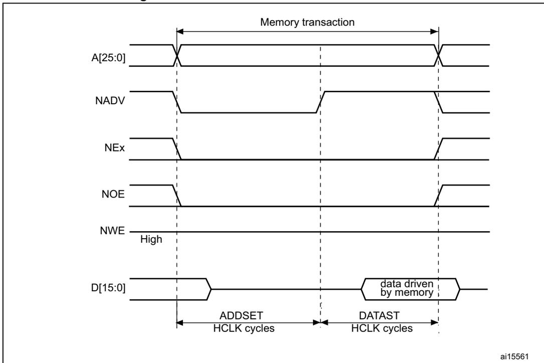
Figure 209. Mode2 write accesses
![Timing diagram for Mode2 write accesses showing signals A[25:0], NADV, NEx, NOE, NWE, and D[15:0] over time. The diagram illustrates the memory transaction phases: address setup (ADDSET), data drive (DATAST), and clock cycle (1HCLK).](/RM0041-STM32F100/89df66c56c95d3d71663553adbf6343b_img.jpg)
This timing diagram illustrates Mode2 write accesses. The signals shown are A[25:0] (address), NADV (address valid), NEx (external memory write enable), NOE (output enable), NWE (write enable), and D[15:0] (data). The timing parameters are defined as follows:
- Memory transaction: The duration from the start of the address setup to the end of the data drive.
- ADDSET: Address setup time in HCLK cycles.
- DATAST: Data drive time in HCLK cycles.
- 1HCLK: One system clock cycle.
The diagram shows the following sequence of events:
- The address A[25:0] is driven and NADV goes low.
- After a delay of ADDSET HCLK cycles, the data D[15:0] is driven by the FSMC.
- Simultaneously, NWE goes low to initiate the write.
- The data remains driven for a duration of (DATAST + 1) HCLK cycles.
- At the end of the data drive, NWE goes high and NOE goes low.
- The signals return to their initial states after another 1HCLK cycle.
ai15562
Figure 210. Mode B write accesses
This timing diagram illustrates Mode B write accesses. The signals and timing parameters are identical to Figure 209, but the sequence of events differs:
- The address A[25:0] is driven and NADV goes low.
- After a delay of ADDSET HCLK cycles, the data D[15:0] is driven by the FSMC.
- Simultaneously, NWE goes low to initiate the write.
- The data remains driven for a duration of (DATAST + 1) HCLK cycles.
- At the end of the data drive, NWE goes high and NOE goes low.
- The signals return to their initial states after another 1HCLK cycle.
ai15563
The differences with mode1 are the toggling of NWE and the independent read and write timings when extended mode is set (Mode B).
Table 103. FSMC_BCRx bit fields
| Bit number | Bit name | Value to set |
|---|---|---|
| 31-20 | Reserved | 0x000 |
| 19 | CBURSTRW | 0x0 (no effect on asynchronous mode) |
| 18:16 | Reserved | 0x0 (no effect on asynchronous mode) |
| 15 | ASYNCWAIT | Set to 1 if the memory supports this feature. Otherwise keep at 0. |
| 14 | EXTMOD | 0x1 for mode B, 0x0 for mode 2 |
| 13 | WAITEN | 0x0 (no effect on asynchronous mode) |
| 12 | WREN | As needed |
| 11 | WAITCFG | Don't care |
| 10 | WRAPMOD | 0x0 |
| 9 | WAITPOL | Meaningful only if bit 15 is 1 |
| 8 | BURSTEN | 0x0 |
| 7 | Reserved | 0x1 |
| 6 | FACCEN | 0x1 |
| 5-4 | MWID | As needed |
| 3-2 | MTYP[0:1] | 0x2 (NOR flash memory) |
| 1 | MUXEN | 0x0 |
| 0 | MBKEN | 0x1 |
Table 104. FSMC_BTRx bit fields
| Bit number | Bit name | Value to set |
|---|---|---|
| 31:30 | Reserved | 0x0 |
| 29:28 | ACCMOD | 0x1 |
| 27:24 | DATLAT | Don't care |
| 23:20 | CLKDIV | Don't care |
| 19:16 | BUSTURN | Time between NEx high to NEx low (BUSTURN HCLK) |
| 15:8 | DATAST | Duration of the second access phase (DATAST HCLK cycles) for read accesses. |
| 7-4 | ADDHLD | Don't care |
| 3-0 | ADDSET[3:0] | Duration of the first access phase (ADDSET HCLK cycles) for read accesses. Minimum value for ADDSET is 0. |
Table 105. FSMC_BWTRx bit fields
| Bit number | Bit name | Value to set |
|---|---|---|
| 31:30 | Reserved | 0x0 |
| 29:28 | ACCMOD | 0x1 |
| 27:24 | DATLAT | Don't care |
| 23:20 | CLKDIV | Don't care |
| 19:16 | BUSTURN | Time between NEx high to NEx low (BUSTURN HCLK) |
| 15:8 | DATAST | Duration of the second access phase (DATAST+1 HCLK cycles for write accesses, |
| 7:4 | ADDHLD | Don't care |
| 3:0 | ADDSET[3:0] | Duration of the first access phase (ADDSET HCLK cycles) for write accesses. Minimum value for ADDSET is 0. |
Note: The FSMC_BWTRx register is valid only if extended mode is set (mode B), otherwise all its content is don't care.
Mode C - NOR flash - OE toggling
Figure 211. Mode C read accesses
The diagram illustrates the timing for Mode C read accesses. It shows the following signals over time:
- A[25:0] : Address lines, which are stable during the memory transaction.
- NADV : Address Valid signal, which goes low to indicate valid address and data, and goes high to indicate the end of the transaction.
- NEx : Next address signal, which goes low to start the transaction and goes high to end it.
- NOE : Output Enable signal, which goes low to enable data output and goes high to disable it.
- NWE : Write Enable signal, which remains high throughout the read transaction.
- D[15:0] : Data lines, which are driven by memory when NOE is low.
The transaction is divided into two phases by vertical dashed lines:
- ADDSET HCLK cycles : The first phase where the address is set and data is driven by memory.
- DATAST HCLK cycles : The second phase where data continues to be driven by memory.
A horizontal double-headed arrow at the top indicates the entire duration as the "Memory transaction". The data on the D[15:0] lines is labeled "data driven by memory" during the active phases.
ai15564
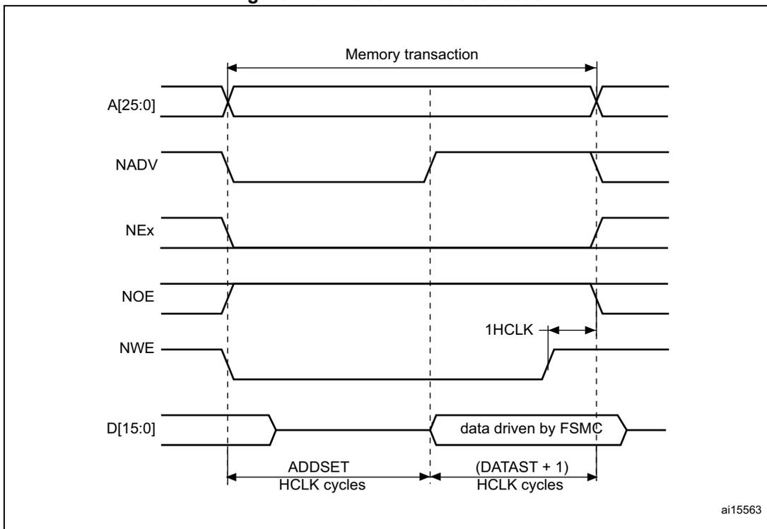
Figure 212. Mode C write accesses
![Timing diagram for Mode C write accesses showing address (A[25:0]), NADV, NEx, NOE, NWE, and data (D[15:0]) signals over time. The diagram illustrates the memory transaction duration, ADDSET time, and (DATAST + 1) time in HCLK cycles. Data is driven by the FSMC.](/RM0041-STM32F100/f7112b13310db11b41e497429848fba2_img.jpg)
The diagram shows the timing for Mode C write accesses. The signals shown are A[25:0], NADV, NEx, NOE, NWE, and D[15:0]. The memory transaction starts when A[25:0] is valid and NADV goes low. It ends when NADV goes high. NEx is low during the transaction. NOE is high during the transaction. NWE is low during the data write phase. D[15:0] is driven by the FSMC during the data write phase. The ADDSET time is the duration from the start of the transaction to the start of the data write phase, measured in HCLK cycles. The (DATAST + 1) time is the duration of the data write phase, measured in HCLK cycles. A 1HCLK cycle is also indicated.
The differences compared with mode1 are the toggling of NOE and the independent read and write timings.
Table 106. FSMC_BCRx bit fields
| Bit No. | Bit name | Value to set |
|---|---|---|
| 31-20 | Reserved | 0x000 |
| 19 | CBURSTRW | 0x0 (no effect on asynchronous mode) |
| 18:16 | CPSIZE | 0x0 (no effect on asynchronous mode) |
| 15 | ASYNCWAIT | Set to 1 if the memory supports this feature. Otherwise keep at 0. |
| 14 | EXTMOD | 0x1 |
| 13 | WAITEN | 0x0 (no effect on asynchronous mode) |
| 12 | WREN | As needed |
| 11 | WAITCFG | Don't care |
| 10 | WRAPMOD | 0x0 |
| 9 | WAITPOL | Meaningful only if bit 15 is 1 |
| 8 | BURSTEN | 0x0 |
| 7 | Reserved | 0x1 |
| 6 | FACCEN | 0x1 |
| 5-4 | MWID | As needed |
| 3-2 | MTYP[0:1] | 0x2 (NOR flash memory) |
| Bit No. | Bit name | Value to set |
|---|---|---|
| 1 | MUXEN | 0x0 |
| 0 | MBKEN | 0x1 |
| Bit number | Bit name | Value to set |
|---|---|---|
| 31:30 | Reserved | 0x0 |
| 29:28 | ACCMOD | 0x2 |
| 27:24 | DATLAT | 0x0 |
| 23:20 | CLKDIV | 0x0 |
| 19:16 | BUSTURN | Time between NEx high to NEx low (BUSTURN HCLK) |
| 15:8 | DATAST | Duration of the second access phase (DATAST HCLK cycles) for read accesses. |
| 7:4 | ADDHLD | Don't care |
| 3:0 | ADDSET[3:0] | Duration of the first access phase (ADDSET HCLK cycles) for read accesses. Minimum value for ADDSET is 0. |
| Bit number | Bit name | Value to set |
|---|---|---|
| 31:30 | Reserved | 0x0 |
| 29:28 | ACCMOD | 0x2 |
| 27:24 | DATLAT | Don't care |
| 23:20 | CLKDIV | Don't care |
| 19:16 | BUSTURN | Time between NEx high to NEx low (BUSTURN HCLK) |
| 15:8 | DATAST | Duration of the second access phase (DATAST+1 HCLK cycles for write accesses, |
| 7:4 | ADDHLD | Don't care |
| 3:0 | ADDSET[3:0] | Duration of the first access phase (ADDSET HCLK cycles) for write accesses. Minimum value for ADDSET is 0. |
Mode D - asynchronous access with extended address
Figure 213. Mode D read accesses
![Timing diagram for Mode D read accesses showing signals A[25:0], NADV, NEx, NOE, NWE, and D[15:0] over time. It details the memory transaction phases: ADDSET, ADDHLD, and DATAST in HCLK cycles.](/RM0041-STM32F100/be2643f91486994a2c497dbb48a9c7ac_img.jpg)
This timing diagram illustrates a read access in Mode D. The signals shown are address lines A[25:0], address valid (NADV), next address (NEx), output enable (NOE), write enable (NWE), and data lines D[15:0]. The NWE signal remains high throughout the transaction. The memory transaction is divided into three phases measured in HCLK cycles: ADDSET (from the falling edge of NADV to the rising edge of NADV), ADDHLD (from the rising edge of NADV to the falling edge of NOE), and DATAST (from the falling edge of NOE to the rising edge of NEx). During the DATAST phase, the data is driven by the memory. Reference code ai15566 is present in the bottom right.
Figure 214. Mode D write accesses
![Timing diagram for Mode D write accesses showing signals A[25:0], NADV, NEx, NOE, NWE, and D[15:0] over time. It details the memory transaction phases: ADDSET, ADDHLD, and (DATAST+ 1) in HCLK cycles, with data driven by FSMC.](/RM0041-STM32F100/3026e6058ee399b7a9aa7d43f85a4a23_img.jpg)
This timing diagram illustrates a write access in Mode D. The signals shown are address lines A[25:0], address valid (NADV), next address (NEx), output enable (NOE), write enable (NWE), and data lines D[15:0]. The NOE signal remains high throughout the transaction. The memory transaction is divided into three phases measured in HCLK cycles: ADDSET (from the falling edge of NADV to the rising edge of NADV), ADDHLD (from the rising edge of NADV to the falling edge of NWE), and (DATAST+ 1) (from the falling edge of NWE to the rising edge of NEx). During the (DATAST+ 1) phase, the data is driven by the FSMC. A 1HCLK cycle is indicated between the falling edge of NWE and the rising edge of NEx. Reference code ai15567 is present in the bottom right.
The differences with mode1 are the toggling of NOE that goes on toggling after NADV changes and the independent read and write timings.
Table 109. FSMC_BCRx bit fields
| Bit No. | Bit name | Value to set |
|---|---|---|
| 31:20 | Reserved | 0x000 |
| 19 | CBURSTRW | 0x0 (no effect on asynchronous mode) |
| 18:16 | CPSIZE | 0x0 (no effect on asynchronous mode) |
| 15 | ASYNCWAIT | Set to 1 if the memory supports this feature. Otherwise keep at 0. |
| 14 | EXTMOD | 0x1 |
| 13 | WAITEN | 0x0 (no effect on asynchronous mode) |
| 12 | WREN | As needed |
| 11 | WAITCFG | Don't care |
| 10 | WRAPMOD | 0x0 |
| 9 | WAITPOL | Meaningful only if bit 15 is 1 |
| 8 | BURSTEN | 0x0 |
| 7 | Reserved | 0x1 |
| 6 | FACCEN | Set according to memory support |
| 5:4 | MWID | As needed |
| 3:2 | MTYP[0:1] | As needed |
| 1 | MUXEN | 0x0 |
| 0 | MBKEN | 0x1 |
Table 110. FSMC_BTRx bit fields
| Bit No. | Bit name | Value to set |
|---|---|---|
| 31:30 | Reserved | 0x0 |
| 29:28 | ACCMOD | 0x3 |
| 27:24 | DATLAT | Don't care |
| 23:20 | CLKDIV | Don't care |
| 19:16 | BUSTURN | Time between NEx high to NEx low (BUSTURN HCLK) |
| 15:8 | DATAST | Duration of the second access phase (DATAST HCLK cycles) for read accesses. |
| 7:4 | ADDHLD | Duration of the middle phase of the read access (ADDHLD HCLK cycles) |
| 3:0 | ADDSET[3:0] | Duration of the first access phase (ADDSET HCLK cycles) for read accesses. Minimum value for ADDSET is 1. |
Table 111. FSMC_BWTRx bit fields
| Bit No. | Bit name | Value to set |
|---|---|---|
| 31:30 | Reserved | 0x0 |
| 29:28 | ACCMOD | 0x3 |
| 27:24 | DATLAT | 0x0 |
| 23:20 | CLKDIV | 0x0 |
| 19:16 | BUSTURN | Time between NEx high to NEx low (BUSTURN HCLK) |
| 15:8 | DATAST | Duration of the second access phase |
| 7:4 | ADDHLD | Duration of the middle phase of the write access (ADDHLD HCLK cycles) |
| 3:0 | ADDSET[3:0] | Duration of the first access phase . Minimum value for ADDSET is 1. |
Muxed mode - multiplexed asynchronous access to NOR flash memory
Figure 215. Multiplexed read accesses
![Timing diagram for multiplexed read accesses in NOR flash memory. The diagram shows the relationship between address lines A[25:16], control signals NADV, NEx, NOE, NWE, and data lines AD[15:0] over time. The address lines are active during the first access phase (ADDSET). The data lines are driven by memory during the second access phase (DATAST). The middle phase (ADDHLD) is the duration of the middle phase of the write access. The memory transaction is shown as a sequence of these three phases.](/RM0041-STM32F100/4909930158e286984ba2f069b44323f4_img.jpg)
The timing diagram illustrates the multiplexed read access sequence. The address lines A[25:16] are active during the first access phase (ADDSET). The data lines AD[15:0] are driven by memory during the second access phase (DATAST). The middle phase (ADDHLD) is the duration of the middle phase of the write access. The memory transaction is shown as a sequence of these three phases.
Key signals and phases shown:
- A[25:16]: Address lines, active during the first access phase (ADDSET).
- NADV: Address Valid signal, active low.
- NEx: Address/Command Enable signal, active low.
- NOE: Output Enable signal, active low.
- NWE: Write Enable signal, active low (shown as High in the diagram).
- AD[15:0]: Data lines, driven by memory during the second access phase (DATAST).
- Phases:
- ADDSET: Duration of the first access phase (HCLK cycles).
- ADDHLD: Duration of the middle phase of the write access (HCLK cycles).
- DATAST: Duration of the second access phase (HCLK cycles).
ai15568
Figure 216. Multiplexed write accesses
![Timing diagram for multiplexed write accesses showing address, data, and control signals over time. The diagram includes signals A[25:16], NADV, NEx, NOE, NWE, and AD[15:0]. The AD[15:0] signal is shown in two phases: 'Lower address' and 'data driven by FSMC'. Timing parameters include ADDSET, ADDHLD, and (DATAST + 1) in HCLK cycles. A 1HCLK cycle is also indicated.](/RM0041-STM32F100/d38d93e51dc86c721bbeb5b06534d74d_img.jpg)
The diagram illustrates the timing for multiplexed write accesses. The address lines A[25:16] are active during the 'Lower address' phase of the AD[15:0] signal. The NADV signal is active low during the address phase. The NEx signal is active low throughout the transaction. The NOE signal is active low during the data phase. The NWE signal is active low during the data phase. The AD[15:0] signal drives the lower address bytes during the first phase and data during the second phase. The timing parameters are defined as follows: ADDSET is the time from the start of the address phase to the start of the data phase; ADDHLD is the time from the start of the data phase to the start of the next phase; (DATAST + 1) is the duration of the data phase. A 1HCLK cycle is shown as a reference.
The difference with mode D is the drive of the lower address byte(s) on the databus.
Table 112. FSMC_BCRx bit fields
| Bit No. | Bit name | Value to set |
|---|---|---|
| 31-21 | Reserved | 0x000 |
| 19 | CBURSTRW | 0x0 (no effect on asynchronous mode) |
| 18:16 | CPSIZE | 0x0 (no effect on asynchronous mode) |
| 15 | ASYNCWAIT | Set to 1 if the memory supports this feature. Otherwise keep at 0. |
| 14 | EXTMOD | 0x0 |
| 13 | WAITEN | 0x0 (no effect on asynchronous mode) |
| 12 | WREN | As needed |
| 11 | WAITCFG | Don't care |
| 10 | WRAPMOD | 0x0 |
| 9 | WAITPOL | Meaningful only if bit 15 is 1 |
| 8 | BURSTEN | 0x0 |
| 7 | Reserved | 0x1 |
| 6 | FACCEN | 0x1 |
| 5-4 | MWID | As needed |
| 3-2 | MTYP[0:1] | 0x2 (NOR flash memory) |
| Bit No. | Bit name | Value to set |
|---|---|---|
| 1 | MUXEN | 0x1 |
| 0 | MBKEN | 0x1 |
| Bit No. | Bit name | Value to set |
|---|---|---|
| 31:30 | Reserved | 0x0 |
| 29:28 | ACCMOD | 0x0 |
| 27:24 | DATLAT | Don't care |
| 23:20 | CLKDIV | Don't care |
| 19:16 | BUSTURN | Time between NEx high to NEx low (BUSTURN HCLK) |
| 15:8 | DATAST | Duration of the second access phase (DATAST HCLK cycles for read accesses and DATAST+1 HCLK cycles for write accesses). |
| 7:4 | ADDHLD | Duration of the middle phase of the access (ADDHLD HCLK cycles). |
| 3:0 | ADDSET[3:0] | Duration of the first access phase (ADDSET HCLK cycles). Minimum value for ADDSET is 1. |
WAIT management in asynchronous accesses
If the asynchronous memory asserts a WAIT signal to indicate that it is not yet ready to accept or to provide data, the ASYNCWAIT bit has to be set in FSMC_BCRx register.
If the WAIT signal is active (high or low depending on the WAITPOL bit), the second access phase (Data setup phase) programmed by the DATAST bits, is extended until WAIT becomes inactive. Unlike the data setup phase, the first access phases (Address setup and Address hold phases), programmed by the ADDSET[3:0] and ADDHLD bits, are not WAIT sensitive and so they are not prolonged.
The data setup phase (DATAST in the FSMC_BTRx register) must be programmed so that WAIT can be detected 4 HCLK cycles before the end of memory transaction. The following cases must be considered:
- 1. DATAST in FSMC_BTRx register) Memory asserts the WAIT signal aligned to NOE/NWE which toggles:
- 2. Memory asserts the WAIT signal aligned to NEx (or NOE/NWE not toggling):
if
then
otherwise
where max_wait_assertion_time is the maximum time taken by the memory to assert the WAIT signal once NEx/NOE/NWE is low.
Figure 217 and Figure 218 show the number of HCLK clock cycles that are added to the memory access after WAIT is released by the asynchronous memory (independently of the above cases).
Figure 217. Asynchronous wait during a read access
![Timing diagram for asynchronous wait during a read access. It shows signals A[25:0], NEx, NWAIT, NOE, and D[15:0] over time. The diagram is divided into 'address phase' and 'data setup phase'. NWAIT is shown as 'don't care' in the address phase and active in the data setup phase. Data is driven by memory for 4HCLK cycles.](/RM0041-STM32F100/0f7643b1ebd8d421fe504ec39d6283a6_img.jpg)
The timing diagram illustrates the sequence of signals during a read access with an asynchronous wait state.
-
A[25:0]
: Address lines, stable during the address phase and high-impedance during the data setup phase.
-
NEx
: Address Status signal, goes low at the start of the address phase and returns high at the start of the data setup phase.
-
NWAIT
: Wait signal, its polarity is 'don't care' during the address phase. In the data setup phase, it is shown as active-low (going low) and then returning high before the data is driven.
-
NOE
: Output Enable signal, goes low at the start of the data setup phase and returns high after the data is driven.
-
D[15:0]
: Data lines, which are high-impedance until the 'data driven by memory' period begins. This period lasts for 4HCLK clock cycles.
The entire sequence is labeled as a 'Memory transaction'.
- 1. NWAIT polarity depends on WAITPOL bit setting in FSMC_BCRx register.
Figure 218. Asynchronous wait during a write access
![Timing diagram for asynchronous wait during a write access. It shows signals A[25:0], NEx, NWAIT, NWE, and D[15:0] over time. The diagram is divided into 'address phase' and 'data setup phase'. NWAIT is shown as 'don't care' in both phases. D[15:0] is 'data driven by FSMC' during the data setup phase. Timing markers include 1HCLK and 3HCLK.](/RM0041-STM32F100/9a229d9af25dc7a5f8476b85eb070b89_img.jpg)
The timing diagram illustrates the signal states during a write access with an asynchronous wait. The signals shown are:
- A[25:0] : Address bus, active during the address phase.
- NEx : Address/Command/Write Enable signal, active low.
- NWAIT : Asynchronous wait signal, shown as 'don't care' in both address and data setup phases.
- NWE : Write Enable signal, active low.
- D[15:0] : Data bus, driven by FSMC during the data setup phase.
The memory transaction is divided into two phases: address phase and data setup phase . The data setup phase duration is marked as 3HCLK . A 1HCLK period is also indicated. The diagram is labeled with ai15797c in the bottom right corner.
- 1. NWAIT polarity depends on WAITPOL bit setting in FSMC_BCRx register.
20.5.5 Synchronous transactions
The memory clock, CLK, is a submultiple of HCLK according to the value of parameter CLKDIV.
NOR flash memories specify a minimum time from NADV assertion to CLK high. To meet this constraint, the FSMC does not issue the clock to the memory during the first internal clock cycle of the synchronous access (before NADV assertion). This guarantees that the rising edge of the memory clock occurs in the middle of the NADV low pulse.
Data latency versus NOR flash latency
The data latency is the number of cycles to wait before sampling the data. The DATLAT value must be consistent with the latency value specified in the NOR flash configuration register. The FSMC does not include the clock cycle when NADV is low in the data latency count.
Caution: Some NOR flash memories include the NADV Low cycle in the data latency count, so the exact relation between the latency and the FSMC DATLAT parameter can be either of:
- • NOR flash latency = (DATLAT + 2) CLK clock cycles
- • NOR flash latency = (DATLAT + 3) CLK clock cycles
Some recent memories assert NWAIT during the latency phase. In such cases DATLAT can be set to its minimum value. As a result, the FSMC samples the data and waits long enough to evaluate if the data are valid. Thus the FSMC detects when the memory exits latency and real data are taken.
Other memories do not assert NWAIT during latency. In this case the latency must be set correctly for both the FSMC and the memory, otherwise invalid data are mistaken for good data, or valid data are lost in the initial phase of the memory access.
Single-burst transfer
When the selected bank is configured in burst mode for synchronous accesses, if for example an AHB single-burst transaction is requested on 16-bit memories, the FSMC performs a burst transaction of length 1 (if the AHB transfer is 16-bit), or length 2 (if the AHB transfer is 32-bit) and de-assert the chip select signal when the last data is strobed.
Clearly, such a transfer is not the most efficient in terms of cycles (compared to an asynchronous read). Nevertheless, a random asynchronous access would first require to re-program the memory access mode, which would altogether last longer.
Cross boundary page for Cellular RAM 1.5
Cellular RAM 1.5 does not allow burst access to cross the page boundary. The FSMC controller allows to split automatically the burst access when the memory page size is reached by configuring the CPSIZE bits in the FSMC_BCR1 register following the memory page size.
Wait management
For synchronous NOR flash memories, NWAIT is evaluated after the programmed latency period, (DATLAT+2) CLK clock cycles.
If NWAIT is sensed active (low level when WAITPOL = 0, high level when WAITPOL = 1), wait states are inserted until NWAIT is sensed inactive (high level when WAITPOL = 0, low level when WAITPOL = 1).
When NWAIT is inactive, the data is considered valid either immediately (bit WAITCFG = 1) or on the next clock edge (bit WAITCFG = 0).
During wait-state insertion via the NWAIT signal, the controller continues to send clock pulses to the memory, keeping the chip select and output enable signals valid, and does not consider the data valid.
There are two timing configurations for the NOR flash NWAIT signal in burst mode:
- • Flash memory asserts the NWAIT signal one data cycle before the wait state (default after reset)
- • Flash memory asserts the NWAIT signal during the wait state
These two NOR flash wait state configurations are supported by the FSMC, individually for each chip select, thanks to the WAITCFG bit in the FSMC_BCRx registers (x = 0..3).
Figure 219. Wait configurations
![Timing diagram for Figure 219. Wait configurations. The diagram shows a memory transaction as a burst of 4 half words. It includes signal waveforms for HCLK, CLK, A[25:16], NADV, NWAIT (WAITCFG = 0), NWAIT (WAITCFG = 1), and A/D[15:0]. The address aaddr[25:16] is shown on the A[25:16] line. The data lines A/D[15:0] show aaddr[15:0] followed by three data cycles. The first data cycle is followed by an 'inserted wait state' indicated by a double-width box. The NWAIT signal is shown in two states: WAITCFG = 0, where it is active (low) during the first data cycle and inactive (high) during the wait state; and WAITCFG = 1, where it is active (low) during the wait state and inactive (high) during the first data cycle. The diagram is labeled ai15798b.](/RM0041-STM32F100/68a89502fe7d6294179a0a3668f50359_img.jpg)
Timing diagram illustrating wait configurations for a memory transaction (burst of 4 half words). The diagram shows the relationship between HCLK, CLK, Address (A[25:16]), NADV, NWAIT (WAITCFG = 0 and WAITCFG = 1), and Data (A/D[15:0]).
The address is labeled aaddr[25:16]. The data is labeled aaddr[15:0] and data i .
The inserted wait state is indicated by a double-width box in the data sequence.
ai15798b
Figure 220. Synchronous multiplexed read mode - NOR, PSRAM (CRAM)
![Timing diagram for synchronous multiplexed read mode. It shows signals HCLK, CLK, A[25:16] (addr[25:16]), NEx, NOE, NWE (High), NADV, NWAIT (WAITCFG=0), and A/D[15:0] (Addr[15:0], data). The diagram illustrates the sequence of address, data, and wait states over clock cycles. A memory transaction is defined as a burst of 4 half words. The address is valid for 1 clock cycle, followed by data for 1 clock cycle. The interval between address and data is (DATLAT + 2) CLK cycles. An inserted wait state is shown between the second and third data cycles. Data strobes are indicated for each data cycle. The diagram is labeled ai17723f.](/RM0041-STM32F100/bdeafd3c63bd71bef3f0f7269fa0ebfa_img.jpg)
- 1. Byte lane outputs BL are not shown; for NOR access, they are held high, and, for PSRAM (CRAM) access, they are held low.
- 2. NWAIT polarity is set to 0.
Table 114. FSMC_BCRx bit fields
| Bit No. | Bit name | Value to set |
|---|---|---|
| 31-20 | Reserved | 0x000 |
| 19 | CBURSTRW | No effect on synchronous read |
| 18-16 | CPSIZE | As needed (0x1 for CRAM 1.5) |
| 15 | ASCYWAIT | 0x0 |
| 14 | EXTMOD | 0x0 |
| 13 | WAITEN | Set to 1 if the memory supports this feature, otherwise keep at 0. |
| 12 | WREN | no effect on synchronous read |
| 11 | WAITCFG | to be set according to memory |
| 10 | WRAPMOD | 0x0 |
| 9 | WAITPOL | to be set according to memory |
| 8 | BURSTEN | 0x1 |
| 7 | Reserved | 0x1 |
| 6 | FACCEN | Set according to memory support (NOR flash memory) |
| 5-4 | MWID | As needed |
| Bit No. | Bit name | Value to set |
|---|---|---|
| 3-2 | MTYP[0:1] | 0x1 or 0x2 |
| 1 | MUXEN | As needed |
| 0 | MBKEN | 0x1 |
| Bit No. | Bit name | Value to set |
|---|---|---|
| 31:30 | Reserved | 0x0 |
| 29:28 | ACCMOD | 0x0 |
| 27-24 | DATLAT | Data latency |
| 23-20 | CLKDIV | 0x0 to get CLK = HCLK (not supported) 0x1 to get CLK = 2 × HCLK .. |
| 19-16 | BUSTURN | Time between NEx high to NEx low (BUSTURN HCLK) |
| 15-8 | DATAST | Don't care |
| 7-4 | ADDHLD | Don't care |
| 3-0 | ADDSET[3:0] | Don't care |
Figure 221. Synchronous multiplexed write mode - PSRAM (CRAM)
![Timing diagram for synchronous multiplexed write mode. It shows signals HCLK, CLK, A[25:16] (addr[25:16]), NEx, NOE (Hi-Z), NWE, NADV, NWAIT (WAITCFG = 0), and A/D[15:0] (Addr[15:0], data). The diagram illustrates a memory transaction as a burst of 2 half words. The address is latched on the rising edge of CLK. Data is written on the falling edge of CLK. The NWAIT signal is used to insert a wait state. The diagram is labeled ai14731f.](/RM0041-STM32F100/e27a38334fea3b8134a7f6ab6ae8b39d_img.jpg)
- 1. Memory must issue NWAIT signal one cycle in advance, accordingly WAITCFG must be programmed to 0.
- 2. NWAIT polarity is set to 0.
- 3. Byte Lane (NBL) outputs are not shown, they are held low while NEx is active.
Table 116. FSMC_BCRx bit fields
| Bit No. | Bit name | Value to set |
|---|---|---|
| 31-20 | Reserved | 0x000 |
| 19 | CBURSTRW | 0x1 |
| 18-16 | CPSIZE | As needed (0x1 for CRAM 1.5) |
| 15 | ASYNCWAIT | 0x0 |
| 14 | EXTMOD | 0x0 |
| 13 | WAITEN | Set to 1 if the memory supports this feature, otherwise keep at 0. |
| 12 | WREN | 0x1 |
| 11 | WAITCFG | 0x0 |
| 10 | WRAPMOD | 0x0 |
| Bit No. | Bit name | Value to set |
|---|---|---|
| 9 | WAITPOL | to be set according to memory |
| 8 | BURSTEN | no effect on synchronous write |
| 7 | Reserved | 0x1 |
| 6 | FACCEN | Set according to memory support |
| 5-4 | MWID | As needed |
| 3-2 | MTYP[0:1] | 0x1 |
| 1 | MUXEN | As needed |
| 0 | MBKEN | 0x1 |
| Bit No. | Bit name | Value to set |
|---|---|---|
| 31:30 | Reserved | 0x0 |
| 29:28 | ACCMOD | 0x0 |
| 27-24 | DATLAT | Data latency |
| 23-20 | CLKDIV | 0x0 to get CLK = HCLK (not supported) 0x1 to get CLK = 2 × HCLK |
| 19-16 | BUSTURN | Time between NEx high to NEx low (BUSTURN HCLK) |
| 15-8 | DATAST | Don't care |
| 7-4 | ADDHLD | Don't care |
| 3-0 | ADDSET[3:0] | Don't care |
20.5.6 NOR/PSRAM control registers
The NOR/PSRAM control registers have to be accessed by words (32 bits).
SRAM/NOR-flash chip-select control registers 1..4 (FSMC_BCR1..4)
Address offset: \( 0xA000\ 0000 + 8 * (x - 1) \) , \( x = 1..4 \)
Reset value: 0x0000 30DB for Bank1 and 0x0000 30D2 for Bank 2 to 4
This register contains the control information of each memory bank, used for SRAMs, PSRAM and NOR flash memories.
| 31 | 30 | 29 | 28 | 27 | 26 | 25 | 24 | 23 | 22 | 21 | 20 | 19 | 18 | 17 | 16 | 15 | 14 | 13 | 12 | 11 | 10 | 9 | 8 | 7 | 6 | 5 | 4 | 3 | 2 | 1 | 0 |
|---|---|---|---|---|---|---|---|---|---|---|---|---|---|---|---|---|---|---|---|---|---|---|---|---|---|---|---|---|---|---|---|
| Reserved | CBURSTRW | CPSIZE[2:0] | ASYNCWAIT | EXTMOD | WAITEN | WREN | WAITCFG | WRAPMOD | WAITPOL | BURSTEN | Reserved | FACCEN | MWID[1:0] | MTYP[1:0] | MUXEN | MBKEN | |||||||||||||||
| rw | rw | rw | rw | rw | rw | rw | rw | rw | rw | rw | rw | rw | rw | rw | rw | rw | rw | rw | rw | rw | rw | rw | rw | rw | rw | rw | rw | ||||
Bits 31: 20 Reserved, must be kept at reset value.
Bit 19 CBURSTRW : Write burst enable.
For Cellular RAM (PSRAM) memories, this bit enables the synchronous burst protocol during write operations. The enable bit for synchronous read accesses is the BURSTEN bit in the FSMC_BCRx register.
0: Write operations are always performed in asynchronous mode
1: Write operations are performed in synchronous mode.
Bits 18: 16 CPSIZE[2:0] : CRAM page size.
These are used for Cellular RAM 1.5 which does not allow burst access to cross the address boundaries between pages. When these bits are configured, the FSMC controller splits automatically the burst access when the memory page size is reached (refer to memory datasheet for page size).
000: No burst split when crossing page boundary (default after reset)
001: 128 bytes
010: 256 bytes
011: 512 bytes
100: 1024 bytes
Others: reserved.
Bit 15 ASYNCWAIT : Wait signal during asynchronous transfers
This bit enables/disables the FSMC to use the wait signal even during an asynchronous protocol.
0: NWAIT signal is not taken into account when running an asynchronous protocol (default after reset)
1: NWAIT signal is taken into account when running an asynchronous protocol
Bit 14 EXTMOD: Extended mode enable.This bit enables the FSMC to program the write timings for non-multiplexed asynchronous accesses inside the FSMC_BWTR register, thus resulting in different timings for read and write operations.
0: values inside FSMC_BWTR register are not taken into account (default after reset)
1: values inside FSMC_BWTR register are taken into account
Note: When the extended mode is disabled, the FSMC can operate in Mode1 or Mode2 as follows:
- – Mode 1 is the default mode when the SRAM/PSRAM memory type is selected (MTYP [0:1]=0x0 or 0x01)
- – Mode 2 is the default mode when the NOR memory type is selected (MTYP [0:1]= 0x10).
This bit enables/disables wait-state insertion via the NWAIT signal when accessing the flash memory in synchronous mode.
0: NWAIT signal is disabled (its level not taken into account, no wait state inserted after the programmed flash latency period)
1: NWAIT signal is enabled (its level is taken into account after the programmed flash latency period to insert wait states if asserted) (default after reset)
Bit 12 WREN: Write enable bit.This bit indicates whether write operations are enabled/disabled in the bank by the FSMC:
0: Write operations are disabled in the bank by the FSMC, an AHB error is reported,
1: Write operations are enabled for the bank by the FSMC (default after reset).
Bit 11 WAITCFG: Wait timing configuration.The NWAIT signal indicates whether the data from the memory are valid or if a wait state must be inserted when accessing the flash memory in synchronous mode. This configuration bit determines if NWAIT is asserted by the memory one clock cycle before the wait state or during the wait state:
0: NWAIT signal is active one data cycle before wait state (default after reset),
1: NWAIT signal is active during wait state (not used for PRAM).
Bit 10 WRAPMOD: Wrapped burst mode support.Defines whether the controller splits or not an AHB burst wrap access into two linear accesses. Valid only when accessing memories in burst mode
0: Direct wrapped burst is not enabled (default after reset),
1: Direct wrapped burst is enabled.
Note: This bit has no effect as the CPU and DMA cannot generate wrapping burst transfers.
Bit 9 WAITPOL: Wait signal polarity bit.Defines the polarity of the wait signal from memory. Valid only when accessing the memory in burst mode:
0: NWAIT active low (default after reset),
1: NWAIT active high.
Bit 8 BURSTEN: Burst enable bit.This bit enables/disables synchronous accesses during read operations. It is valid only for synchronous memories operating in burst mode:
0: Burst mode disabled (default after reset). Read accesses are performed in asynchronous mode.
1: Burst mode enable. Read accesses are performed in synchronous mode.
Bit 7 Reserved, must be kept at reset value.
Bit 6 FACCEN : Flash access enable
Enables NOR flash memory access operations.
0: Corresponding NOR flash memory access is disabled
1: Corresponding NOR flash memory access is enabled (default after reset)
Bits 5:4 MWID[1:0] : Memory databus width.
Defines the external memory device width, valid for all type of memories.
00: 8 bits,
01: 16 bits (default after reset),
10: reserved, do not use,
11: reserved, do not use.
Bits 3:2 MTYP[1:0] : Memory type.
Defines the type of external memory attached to the corresponding memory bank:
00: SRAM (default after reset for Bank 2...4)
01: PSRAM (CRAM)
10: NOR flash/OneNAND flash (default after reset for Bank 1)
11: reserved
Bit 1 MUXEN : Address/data multiplexing enable bit.
When this bit is set, the address and data values are multiplexed on the databus, valid only with NOR and PSRAM memories:
0: Address/Data nonmultiplexed
1: Address/Data multiplexed on databus (default after reset)
Bit 0 MBKEN : Memory bank enable bit.
Enables the memory bank. After reset Bank1 is enabled, all others are disabled.
Accessing a disabled bank causes an ERROR on AHB bus.
0: Corresponding memory bank is disabled
1: Corresponding memory bank is enabled
SRAM/NOR-Flash chip-select timing registers 1..4 (FSMC_BTR1..4)
Address offset: \( 0xA000\ 0000 + 0x04 + 8 * (x - 1) \) , \( x = 1..4 \)
Reset value: 0x0FFF FFFF
FSMC_BTRx bits are written by software to add a delay at the end of a read /write transaction. This delay allows matching the minimum time between consecutive transactions ( \( t_{EHEL} \) from NEx high to FSMC_NEx low) and the maximum time required by the memory to free the data bus after a read access ( \( t_{EHQZ} \) ).
This register contains the control information of each memory bank, used for SRAMs, PSRAM and NOR flash memories. If the EXTMOD bit is set in the FSMC_BCRx register, then this register is partitioned for write and read access, that is, 2 registers are available: one to configure read accesses (this register) and one to configure write accesses (FSMC_BWTRx registers).
| 31 | 30 | 29 | 28 | 27 | 26 | 25 | 24 | 23 | 22 | 21 | 20 | 19 | 18 | 17 | 16 | 15 | 14 | 13 | 12 | 11 | 10 | 9 | 8 | 7 | 6 | 5 | 4 | 3 | 2 | 1 | 0 |
|---|---|---|---|---|---|---|---|---|---|---|---|---|---|---|---|---|---|---|---|---|---|---|---|---|---|---|---|---|---|---|---|
| Reserved | ACCMOD[1:0] | DATLAT[3:0] | CLKDIV[3:0] | BURSTURN[3:0] | DATAST[7:0] | ADDHLD[3:0] | ADDSET[3:0] | ||||||||||||||||||||||||
| rw | rw | rw | rw | rw | rw | rw | rw | rw | rw | rw | rw | rw | rw | rw | rw | rw | rw | rw | rw | rw | rw | rw | rw | rw | rw | rw | rw | rw | rw | rw | rw |
Bits 31:30 Reserved, must be kept at reset value.
Bits 29:28 ACCMOD[1:0] : Access mode
Specifies the asynchronous access modes as shown in the timing diagrams. These bits are taken into account only when the EXTMOD bit in the FSMC_BCRx register is 1.
- 00: access mode A
- 01: access mode B
- 10: access mode C
- 11: access mode D
Bits 27:24 DATLAT[3:0] : Data latency for synchronous NOR flash memory (see note below bit description table)
For synchronous NOR flash memory with burst mode enabled, defines the number of memory clock cycles (+2) to issue to the memory before reading/writing the first data.
This timing parameter is not expressed in HCLK periods, but in FSMC_CLK periods. In case of PSRAM (CRAM), this field must be set to 0. In asynchronous NOR flash or SRAM or PSRAM, this value is don't care.
- 0000: Data latency of 2 CLK clock cycles for first burst access
- 1111: Data latency of 17 CLK clock cycles for first burst access (default value after reset)
Bits 23:20 CLKDIV[3:0] : Clock divide ratio (for FSMC_CLK signal)
Defines the period of FSMC_CLK clock output signal, expressed in number of HCLK cycles:
- 0000: Reserved
- 0001: FSMC_CLK period = \( 2 \times \) HCLK periods
- 0010: FSMC_CLK period = \( 3 \times \) HCLK periods
- 1111: FSMC_CLK period = \( 16 \times \) HCLK periods (default value after reset)
In asynchronous NOR flash, SRAM or PSRAM accesses, this value is don't care.
Bits 19:16 BUSTURN[3:0] : Bus turnaround phase durationThese bits are written by software to add a delay at the end of a write-to-read (and read-to write) transaction. The programmed bus turnaround delay is inserted between an asynchronous read (muxed or D mode) or a write transaction and any other asynchronous/synchronous read or write to/from a static bank (for a read operation, the bank can be the same or a different one; for a write operation, the bank can be different except in muxed or D mode).
In some cases, the bus turnaround delay is fixed, whatever the programmed BUSTURN values:
- – No bus turnaround delay is inserted between two consecutive asynchronous write transfers to the same static memory bank except in muxed and D mode.
- – A bus turnaround delay of 1 FSMC clock cycle is inserted between:
- – Two consecutive asynchronous read transfers to the same static memory bank except for muxed and D modes.
- – An asynchronous read to an asynchronous or synchronous write to any static bank or dynamic bank except for muxed and D modes.
- – An asynchronous (modes 1, 2, A, B or C) read and a read operation from another static bank.
- – A bus turnaround delay of 2 FSMC clock cycles is inserted between:
- – Two consecutive synchronous write accesses (in burst or single mode) to the same bank
- – A synchronous write (burst or single) access and an asynchronous write or read transfer to or from static memory bank (the bank can be the same or different in case of a read operation).
- – Two consecutive synchronous read accesses (in burst or single mode) followed by a any synchronous/asynchronous read or write from/to another static memory bank.
- – A bus turnaround delay of 3 FSMC clock cycles is inserted between:
- – Two consecutive synchronous write operations (in burst or single mode) to different static banks.
- – A synchronous write access (in burst or single mode) and a synchronous read access from the same or to a different bank.
0000: BUSTURN phase duration = 0 HCLK clock cycle added
...
1111: BUSTURN phase duration = 15 × HCLK clock cycles (default value after reset)
Bits 15:8 DATAST[7:0] : Data-phase durationThese bits are written by software to define the duration of the data phase (refer to Figure 204 to Figure 216 ), used in asynchronous accesses:
0000 0000: Reserved
0000 0001: DATAST phase duration = 1 × HCLK clock cycles
0000 0010: DATAST phase duration = 2 × HCLK clock cycles
...
1111 1111: DATAST phase duration = 255 × HCLK clock cycles (default value after reset)
For each memory type and access mode data-phase duration, refer to the respective figure ( Figure 204 to Figure 216 ).
Example: Mode1, write access, DATAST=1: Data-phase duration= DATAST+1 = 2 HCLK clock cycles.
Note: In synchronous accesses, this value is don't care.
Bits 7:4 ADDHLD[3:0] : Address-hold phase durationThese bits are written by software to define the duration of the address hold phase (refer to Figure 213 to Figure 216 ), used in mode D and multiplexed accesses:
0000: Reserved
0001: ADDHLD phase duration = 1 × HCLK clock cycle
0010: ADDHLD phase duration = 2 × HCLK clock cycle
...
1111: ADDHLD phase duration = 15 × HCLK clock cycles (default value after reset)
For each access mode address-hold phase duration, refer to the respective figure ( Figure 213 to Figure 216 ).
Note: In synchronous accesses, this value is not used, the address hold phase is always 1 memory clock period duration.
Bits 3:0 ADDSET[3:0] : Address setup phase durationThese bits are written by software to define the duration of the address setup phase (refer to Figure 204 to Figure 216 ), used in SRAMs, ROMs and asynchronous NOR flash and PSRAM accesses:
0000: ADDSET phase duration = 0 × HCLK clock cycle
...
1111: ADDSET phase duration = 15 × HCLK clock cycles (default value after reset)
For each access mode address setup phase duration, refer to the respective figure (refer to Figure 204 to Figure 216 ).
Note: In synchronous NOR flash and PSRAM accesses, this value is don't care.
Note: PSRAMs (CRAMs) have a variable latency due to internal refresh. Therefore these memories issue the NWAIT signal during the whole latency phase to prolong the latency as needed.
With PSRAMs (CRAMs) the DATLAT field must be set to 0, so that the FSMC exits its latency phase soon and starts sampling NWAIT from memory, then starts to read or write when the memory is ready.
This method can be used also with the latest generation of synchronous flash memories that issue the NWAIT signal, unlike older flash memories (check the datasheet of the specific flash memory being used).
SRAM/NOR-Flash write timing registers 1..4 (FSMC_BWTR1..4)
Address offset: \( 0xA000\ 0000 + 0x104 + 8 * (x - 1) \) , \( x = 1 \dots 4 \)
Reset value: 0x0FFF FFFF
This register contains the control information of each memory bank, used for SRAMs, PSRAMs and NOR flash memories. This register is active for write asynchronous access only when the EXTMOD bit is set in the FSMC_BCRx register.
| 31 | 30 | 29 | 28 | 27 | 26 | 25 | 24 | 23 | 22 | 21 | 20 | 19 | 18 | 17 | 16 | 15 | 14 | 13 | 12 | 11 | 10 | 9 | 8 | 7 | 6 | 5 | 4 | 3 | 2 | 1 | 0 |
| Res. | ACCM OD[2:0] | Reserved | BUSTURN[3:0] | DATAST[7:0] | ADDHLD[3:0] | ADDSET[3:0] | |||||||||||||||||||||||||
| rw | rw | rw | rw | rw | rw | rw | rw | rw | rw | rw | rw | rw | rw | rw | rw | rw | rw | rw | rw | rw | rw | ||||||||||
Bits 31:30 Reserved, must be kept at reset value.
Bits 29:28 ACCMOD[2:0] : Access mode.
Specifies the asynchronous access modes as shown in the next timing diagrams. These bits are taken into account only when the EXTMOD bit in the FSMC_BCRx register is 1.
00: access mode A
01: access mode B
10: access mode C
11: access mode D
Bits 27:20 Reserved, must be kept at reset value.
Bits 19:16 BUSTURN[3:0] : Bus turnaround phase duration
The programmed bus turnaround delay is inserted between an asynchronous write transfer and any other asynchronous/synchronous read or write transfer to/from a static bank (for a read operation, the bank can be the same or a different one; for a write operation, the bank can be different except in r muxed or D mode).
In some cases, the bus turnaround delay is fixed, whatever the programmed BUSTURN values:
- – No bus turnaround delay is inserted between two consecutive asynchronous write transfers to the same static memory bank except in muxed and D mode.
- – A bus turnaround delay of 2 FSMC clock cycles is inserted between:
- – Two consecutive synchronous write accesses (in burst or single mode) to the same bank.
- – A synchronous write transfer (in burst or single mode) and an asynchronous write or read transfer to/from static a memory bank.
- – A bus turnaround delay of 3 FSMC clock cycles is inserted between:
- – Two consecutive synchronous write accesses (in burst or single mode) to different static banks.
- – A synchronous write transfer (in burst or single mode) and a synchronous read from the same or from a different bank.
0000: BUSTURN phase duration = 0 HCLK clock cycle added
...
1111: BUSTURN phase duration = 15 HCLK clock cycles added (default value after reset)
Bits 15:8 DATAST[7:0] : Data-phase duration.
These bits are written by software to define the duration of the data phase (refer to Figure 204 to Figure 216 ), used in asynchronous SRAM, PSRAM and NOR flash memory accesses:
0000 0000: Reserved
0000 0001: DATAST phase duration = 1 × HCLK clock cycles
0000 0010: DATAST phase duration = 2 × HCLK clock cycles
...
1111 1111: DATAST phase duration = 255 × HCLK clock cycles (default value after reset)
Note: In synchronous accesses, this value is don't care.
Bits 7:4 ADDHLD[3:0] : Address-hold phase duration.
These bits are written by software to define the duration of the address hold phase (refer to Figure 213 to Figure 216 ), used in asynchronous multiplexed accesses:
0000: Reserved
0001: ADDHLD phase duration = 1 × HCLK clock cycle
0010: ADDHLD phase duration = 2 × HCLK clock cycle
...
1111: ADDHLD phase duration = 15 × HCLK clock cycles (default value after reset)
Note: In synchronous NOR flash accesses, this value is not used, the address hold phase is always 1 flash clock period duration.
Bits 3:0 ADDSET[3:0] : Address setup phase duration.
These bits are written by software to define the duration of the address setup phase in HCLK cycles (refer to Figure 213 to Figure 216 ), used in asynchronous accessed:
0000: ADDSET phase duration = 0 × HCLK clock cycle
...
1111: ADDSET phase duration = 15 × HCLK clock cycles (default value after reset)
Note: In synchronous NOR flash and PSRAM accesses, this value is don't care.
20.5.7 FSMC register map
The following table summarizes the FSMC registers.
Table 118. FSMC register map
| Offset | Register | 31 | 30 | 29 | 28 | 27 | 26 | 25 | 24 | 23 | 22 | 21 | 20 | 19 | 18 | 17 | 16 | 15 | 14 | 13 | 12 | 11 | 10 | 9 | 8 | 7 | 6 | 5 | 4 | 3 | 2 | 1 | 0 |
|---|---|---|---|---|---|---|---|---|---|---|---|---|---|---|---|---|---|---|---|---|---|---|---|---|---|---|---|---|---|---|---|---|---|
| 0000 | FSMC_BCR1 | Reserved | CBURSTRW | CPSIZE[2:0] | ASYNCWAIT | EXTMOD | WAITEN | WREN | WAITCFG | WRAPMOD | WAITPOL | BURSTEN | Reserved | FACCEN | MWID[1:0] | MTYP[0:1] | MUXEN | MBKEN | |||||||||||||||
| 0008 | FSMC_BCR2 | Reserved | CBURSTRW | CPSIZE[2:0] | ASYNCWAIT | EXTMOD | WAITEN | WREN | WAITCFG | WRAPMOD | WAITPOL | BURSTEN | Reserved | FACCEN | MWID[1:0] | MTYP[0:1] | MUXEN | MBKEN | |||||||||||||||
| 0010 | FSMC_BCR3 | Reserved | CBURSTRW | CPSIZE[2:0] | ASYNCWAIT | EXTMOD | WAITEN | WREN | WAITCFG | WRAPMOD | WAITPOL | BURSTEN | Reserved | FACCEN | MWID[1:0] | MTYP[0:1] | MUXEN | MBKEN | |||||||||||||||
| 0018 | FSMC_BCR4 | Reserved | CBURSTRW | CPSIZE[2:0] | ASYNCWAIT | EXTMOD | WAITEN | WREN | WAITCFG | WRAPMOD | WAITPOL | BURSTEN | Reserved | FACCEN | MWID[1:0] | MTYP[0:1] | MUXEN | MBKEN | |||||||||||||||
| 0004 | FSMC_BTR1 | Res. | ACCMOD[1:0] | DATLAT[3:0] | CLKDIV[3:0] | BUSTURN[3:0] | DATAST[7:0] | ADDHLD[3:0] | ADDSET[3:0] | ||||||||||||||||||||||||
| 000C | FSMC_BTR2 | Res. | ACCMOD[1:0] | DATLAT[3:0] | CLKDIV[3:0] | BUSTURN[3:0] | DATAST[7:0] | ADDHLD[3:0] | ADDSET[3:0] | ||||||||||||||||||||||||
| 0014 | FSMC_BTR3 | Res. | ACCMOD[1:0] | DATLAT[3:0] | CLKDIV[3:0] | BUSTURN[3:0] | DATAST[7:0] | ADDHLD[3:0] | ADDSET[3:0] | ||||||||||||||||||||||||
| 001C | FSMC_BTR4 | Res. | ACCMOD[1:0] | DATLAT[3:0] | CLKDIV[3:0] | BUSTURN[3:0] | DATAST[7:0] | ADDHLD[3:0] | ADDSET[3:0] | ||||||||||||||||||||||||
| 0104 | FSMC_BWTR 1 | Res. | ACCMOD[1:0] | Res. | BUSTURN[3:0] | DATAST[7:0] | ADDHLD[3:0] | ADDSET[3:0] | |||||||||||||||||||||||||
| 010C | FSMC_BWTR 2 | Res. | ACCMOD[1:0] | Res. | BUSTURN[3:0] | DATAST[7:0] | ADDHLD[3:0] | ADDSET[3:0] | |||||||||||||||||||||||||
Table 118. FSMC register map (continued)
| Offset | Register | 31 | 30 | 29 | 28 | 27 | 26 | 25 | 24 | 23 | 22 | 21 | 20 | 19 | 18 | 17 | 16 | 15 | 14 | 13 | 12 | 11 | 10 | 9 | 8 | 7 | 6 | 5 | 4 | 3 | 2 | 1 | 0 |
|---|---|---|---|---|---|---|---|---|---|---|---|---|---|---|---|---|---|---|---|---|---|---|---|---|---|---|---|---|---|---|---|---|---|
| 0114 | FSMC_BWTR 3 | Res. | ACC MOD [1:0] | Res. | BUSTURN[3:0] | DATAST[7:0] | ADDHLD[3:0] | ADDSET[3:0] | |||||||||||||||||||||||||
| 011C | FSMC_BWTR 4 | Res. | ACC MOD [1:0] | Res. | BUSTURN[3:0] | DATAST[7:0] | ADDHLD[3:0] | ADDSET[3:0] | |||||||||||||||||||||||||
Refer to for the register boundary addresses.