17. Real-time clock (RTC)
Low-density value line devices are STM32F100xx microcontrollers where the flash memory density ranges between 16 and 32 Kbytes.
Medium-density value line devices are STM32F100xx microcontrollers where the flash memory density ranges between 64 and 128 Kbytes.
High-density value line devices are STM32F100xx microcontrollers where the flash memory density ranges between 256 and 512 Kbytes.
This section applies to the whole STM32F10xxx family, unless otherwise specified.
17.1 RTC introduction
The real-time clock is an independent timer. The RTC provides a set of continuously running counters which can be used, with suitable software, to provide a clock-calendar function. The counter values can be written to set the current time/date of the system.
The RTC core and clock configuration (RCC_BDCR register) are in the Backup domain, which means that RTC setting and time are kept after reset or wakeup from Standby mode.
After reset, access to the Backup registers and RTC is disabled and the Backup domain (BKP) is protected against possible parasitic write access. To enable access to the Backup registers and the RTC, proceed as follows:
- • enable the power and backup interface clocks by setting the PWREN and BKPEN bits in the RCC_APB1ENR register
- • set the DBP bit the Power Control register (PWR_CR) to enable access to the Backup registers and RTC.
17.2 RTC main features
- • Programmable prescaler: division factor up to \( 2^{20} \)
- • 32-bit programmable counter for long-term measurement
- • Two separate clocks: PCLK1 for the APB1 interface and RTC clock (must be at least four times slower than the PCLK1 clock)
- • The RTC clock source could be any of the following ones:
- – HSE clock divided by 128
- – LSE oscillator clock
- – LSI oscillator clock (refer to Section 6.2.8: RTC clock for details)
- • Two separate reset types:
- – The APB1 interface is reset by system reset
- – The RTC Core (Prescaler, Alarm, Counter and Divider) is reset only by a Backup domain reset (see Section 6.1.3: Backup domain reset on page 72 ).
- • Three dedicated maskable interrupt lines:
- – Alarm interrupt, for generating a software programmable alarm interrupt.
- – Seconds interrupt, for generating a periodic interrupt signal with a programmable period length (up to 1 second).
- – Overflow interrupt, to detect when the internal programmable counter rolls over to zero.
17.3 RTC functional description
17.3.1 Overview
The RTC consists of two main units (see Figure 196 ). The first one (APB1 Interface) is used to interface with the APB1 bus. This unit also contains a set of 16-bit registers accessible from the APB1 bus in read or write mode (for more information refer to Section 17.4: RTC registers ). The APB1 interface is clocked by the APB1 bus clock in order to interface with the APB1 bus.
The other unit (RTC Core) consists of a chain of programmable counters made of two main blocks. The first block is the RTC prescaler block, which generates the RTC time base TR_CLK that can be programmed to have a period of up to 1 second. It includes a 20-bit programmable divider (RTC_Prescaler). Every TR_CLK period, the RTC generates an interrupt (Second Interrupt) if it is enabled in the RTC_CR register. The second block is a 32-bit programmable counter that can be initialized to the current system time. The system time is incremented at the TR_CLK rate and compared with a programmable date (stored in the RTC_ALR register) in order to generate an alarm interrupt, if enabled in the RTC_CR control register.
Figure 196. RTC simplified block diagram
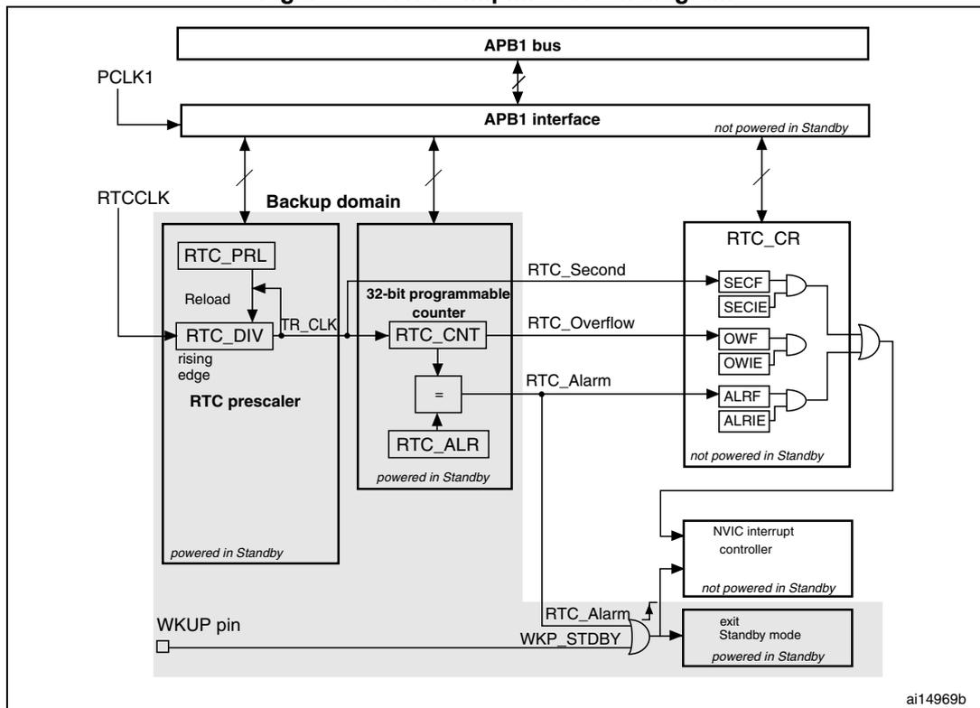
The diagram illustrates the RTC architecture. At the top, the APB1 bus connects to the APB1 interface . The APB1 interface is connected to the Backup domain . The Backup domain contains the RTC prescaler (consisting of RTC_PRL and RTC_DIV blocks) and the 32-bit programmable counter (consisting of RTC_CNT and RTC_ALR blocks). The RTC prescaler generates the TR_CLK signal. The 32-bit programmable counter is connected to the RTC_ALR register. The RTC_CR register contains the SECIF , SECIE , OWF , OWIE , ALRF , and ALRIE flags. The RTC_CR register is connected to the NVIC interrupt controller and the exit Standby mode block. The WKUP pin is connected to the exit Standby mode block. The RTC_CR register is not powered in Standby. The 32-bit programmable counter is powered in Standby. The RTC prescaler is powered in Standby. The APB1 interface is not powered in Standby. The diagram is labeled ai14969b.
17.3.2 Resetting RTC registers
All system registers are asynchronously reset by a System Reset or Power Reset, except for RTC_PRL, RTC_ALR, RTC_CNT, and RTC_DIV.
The RTC_PRL, RTC_ALR, RTC_CNT, and RTC_DIV registers are reset only by a Backup Domain reset. Refer to Section 6.1.3: Backup domain reset .
17.3.3 Reading RTC registers
The RTC core is completely independent from the RTC APB1 interface.
Software accesses the RTC prescaler, counter and alarm values through the APB1 interface but the associated readable registers are internally updated at each rising edge of the RTC clock resynchronized by the RTC APB1 clock. This is also true for the RTC flags.
This means that the first read to the RTC APB1 registers may be corrupted (generally read as 0) if the APB1 interface has previously been disabled and the read occurs immediately after the APB1 interface is enabled but before the first internal update of the registers. This can occur if:
- • A system reset or power reset has occurred
- • The MCU has just woken up from Standby mode (see Section 4.3: Low-power modes )
- • The MCU has just woken up from Stop mode (see Section 4.3: Low-power modes )
In all the above cases, the RTC core has been kept running while the APB1 interface was disabled (reset, not clocked or unpowered).
Consequently when reading the RTC registers, after having disabled the RTC APB1 interface, the software must first wait for the RSF bit (Register Synchronized Flag) in the RTC_CRL register to be set by hardware.
Note that the RTC APB1 interface is not affected by WFI and WFE low-power modes.
17.3.4 Configuring RTC registers
To write in the RTC_PRL, RTC_CNT, RTC_ALR registers, the peripheral must enter Configuration mode. This is done by setting the CNF bit in the RTC_CRL register.
In addition, writing to any RTC register is only enabled if the previous write operation is finished. To enable the software to detect this situation, the RTOFF status bit is provided in the RTC_CR register to indicate that an update of the registers is in progress. A new value can be written to the RTC registers only when the RTOFF status bit value is '1'.
Configuration procedure
- 1. Poll RTOFF, wait until its value goes to '1'
- 2. Set the CNF bit to enter configuration mode
- 3. Write to one or more RTC registers
- 4. Clear the CNF bit to exit configuration mode
- 5. Poll RTOFF, wait until its value goes to '1' to check the end of the write operation.
The write operation only executes when the CNF bit is cleared; it takes at least three RTCCLK cycles to complete.
17.3.5 RTC flag assertion
The RTC Second flag (SECF) is asserted on each RTC Core clock cycle before the update of the RTC Counter.
The RTC Overflow flag (OWF) is asserted on the last RTC Core clock cycle before the counter reaches 0x0000.
The RTC_Alarm and RTC Alarm flag (ALRF) (see Figure 197 ) are asserted on the last RTC Core clock cycle before the counter reaches the RTC Alarm value stored in the Alarm register increased by one (RTC_ALR + 1). The write operation in the RTC Alarm and RTC Second flag must be synchronized by using one of the following sequences:
- • Use the RTC Alarm interrupt and inside the RTC interrupt routine, the RTC Alarm and/or RTC Counter registers are updated.
- • Wait for SECf bit to be set in the RTC Control register. Update the RTC Alarm and/or the RTC Counter register.
Figure 197. RTC second and alarm waveform example with PR=0003, ALARM=00004
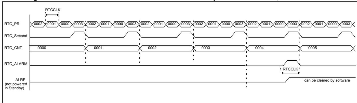
This timing diagram shows the relationship between several RTC signals over a series of RTC_CCLK cycles. The top signal, RTC_PR, shows a periodic pulse train with a period of 4 cycles (labeled 0002, 0001, 0000, 0003). Below it, RTC_Second is a square wave that toggles state on every rising edge of RTC_PR. The RTC_CNT signal shows a sequence of values: 0000, 0001, 0002, 0003, 0004, 0005. The RTC_ALARM signal is shown as a high pulse starting at the counter value 0003 and ending at 0004. The ALRF (not powered in Standby) signal is shown as a pulse that goes high at the counter value 0003 and remains high until it is cleared by software. A label '1 RTCCLK' with a double-headed arrow indicates one clock cycle.
Figure 198. RTC overflow waveform example with PR=0003
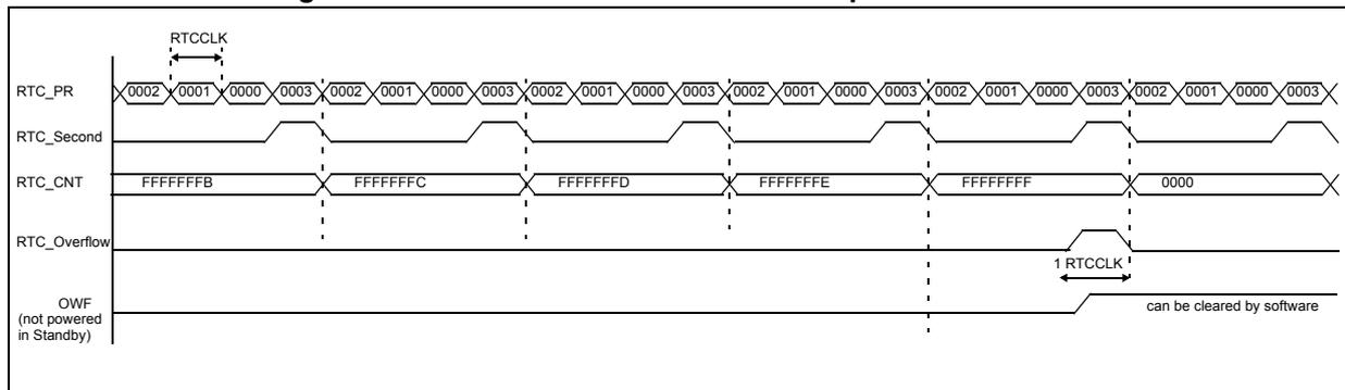
This timing diagram shows the relationship between several RTC signals over a series of RTC_CCLK cycles. The top signal, RTC_PR, shows a periodic pulse train with a period of 4 cycles (labeled 0002, 0001, 0000, 0003). Below it, RTC_Second is a square wave that toggles state on every rising edge of RTC_PR. The RTC_CNT signal shows a sequence of values: FFFFFFFB, FFFFFFFC, FFFFFFFD, FFFFFFFE, FFFFFFFF, 0000. The RTC_Overflow signal is shown as a high pulse starting at the counter value FFFFFFFE and ending at 0000. The OWF (not powered in Standby) signal is shown as a pulse that goes high at the counter value FFFFFFFF and remains high until it is cleared by software. A label '1 RTCCLK' with a double-headed arrow indicates one clock cycle.
17.4 RTC registers
Refer to Section 1.1 on page 32 for a list of abbreviations used in register descriptions.
The peripheral registers can be accessed by half-words (16-bit) or words (32-bit).
17.4.1 RTC control register high (RTC_CRH)
Address offset: 0x00
Reset value: 0x0000

| 15 | 14 | 13 | 12 | 11 | 10 | 9 | 8 | 7 | 6 | 5 | 4 | 3 | 2 | 1 | 0 |
|---|---|---|---|---|---|---|---|---|---|---|---|---|---|---|---|
| Reserved | OWIE | ALRIE | SECIE | ||||||||||||
| rw | rw | rw | |||||||||||||
Bits 15:3 Reserved, forced by hardware to 0.
Bit 2 OWIE : Overflow interrupt enable
0: Overflow interrupt is masked.
1: Overflow interrupt is enabled.
Bit 1 ALRIE : Alarm interrupt enable
0: Alarm interrupt is masked.
1: Alarm interrupt is enabled.
Bit 0 SECIE : Second interrupt enable
0: Second interrupt is masked.
1: Second interrupt is enabled.
These bits are used to mask interrupt requests. Note that at reset all interrupts are disabled, so it is possible to write to the RTC registers to ensure that no interrupt requests are pending after initialization. It is not possible to write to the RTC_CRH register when the peripheral is completing a previous write operation (flagged by RTOFF=0, see Section 17.3.4 ).
The RTC functions are controlled by this control register. Some bits must be written using a specific configuration procedure (see Configuration procedure ).
17.4.2 RTC control register low (RTC_CRL)
Address offset: 0x04
Reset value: 0x0020
| 15 | 14 | 13 | 12 | 11 | 10 | 9 | 8 | 7 | 6 | 5 | 4 | 3 | 2 | 1 | 0 |
|---|---|---|---|---|---|---|---|---|---|---|---|---|---|---|---|
| Reserved | RTOFF | CNF | RSF | OWF | ALRF | SECF | |||||||||
| r | rw | rc_w0 | rc_w0 | rc_w0 | rc_w0 | ||||||||||
Bits 15:6 Reserved, forced by hardware to 0.
Bit 5 RTOFF: RTC operation OFF
With this bit the RTC reports the status of the last write operation performed on its registers, indicating if it has been completed or not. If its value is '0' then it is not possible to write to any of the RTC registers. This bit is read only.
0: Last write operation on RTC registers is still ongoing.
1: Last write operation on RTC registers terminated.
Bit 4 CNF: Configuration flag
This bit must be set by software to enter in configuration mode so as to allow new values to be written in the RTC_CNT, RTC_ALR or RTC_PRL registers. The write operation is only executed when the CNF bit is reset by software after has been set.
0: Exit configuration mode (start update of RTC registers).
1: Enter configuration mode.
Bit 3 RSF: Registers synchronized flag
This bit is set by hardware at each time the RTC_CNT and RTC_DIV registers are updated and cleared by software. Before any read operation after an APB1 reset or an APB1 clock stop, this bit must be cleared by software, and the user application must wait until it is set to be sure that the RTC_CNT, RTC_ALR or RTC_PRL registers are synchronized.
0: Registers not yet synchronized.
1: Registers synchronized.
Bit 2 OWF: Overflow flag
This bit is set by hardware when the 32-bit programmable counter overflows. An interrupt is generated if OWIE=1 in the RTC_CRH register. It can be cleared only by software. Writing '1' has no effect.
0: Overflow not detected
1: 32-bit programmable counter overflow occurred.
Bit 1 ALRF: Alarm flag
This bit is set by hardware when the 32-bit programmable counter reaches the threshold set in the RTC_ALR register. An interrupt is generated if ALRIE=1 in the RTC_CRH register. It can be cleared only by software. Writing '1' has no effect.
0: Alarm not detected
1: Alarm detected
Bit 0 SECF: Second flag
This bit is set by hardware when the 32-bit programmable prescaler overflows, thus incrementing the RTC counter. Hence this flag provides a periodic signal with a period corresponding to the resolution programmed for the RTC counter (usually one second). An interrupt is generated if SECIE=1 in the RTC_CRH register. It can be cleared only by software. Writing '1' has no effect.
0: Second flag condition not met.
1: Second flag condition met.
The functions of the RTC are controlled by this control register. It is not possible to write to the RTC_CR register while the peripheral is completing a previous write operation (flagged by RTOFF=0, see Section 17.3.4: Configuring RTC registers ).
Note: Any flag remains pending until the appropriate RTC_CR request bit is reset by software, indicating that the interrupt request has been granted.
At reset the interrupts are disabled, no interrupt requests are pending and it is possible to write to the RTC registers.
The OWF, ALRF, SECF and RSF bits are not updated when the APB1 clock is not running.
The OWF, ALRF, SECF and RSF bits can only be set by hardware and only cleared by software.
If ALRF = 1 and ALRIE = 1, the RTC global interrupt is enabled. If EXTI Line 17 is also enabled through the EXTI Controller, both the RTC global interrupt and the RTC Alarm interrupt are enabled.
If ALRF = 1, the RTC Alarm interrupt is enabled if EXTI Line 17 is enabled through the EXTI Controller in interrupt mode. When the EXTI Line 17 is enabled in event mode, a pulse is generated on this line (no RTC Alarm interrupt generation).
17.4.3 RTC prescaler load register (RTC_PRLH / RTC_PRLL)
The Prescaler Load registers keep the period counting value of the RTC prescaler. They are write-protected by the RTOFF bit in the RTC_CR register, and a write operation is allowed if the RTOFF value is '1'.
RTC prescaler load register high (RTC_PRLH)
Address offset: 0x08
Write only (see
Section 17.3.4: Configuring RTC registers
)
Reset value: 0x0000

| 15 | 14 | 13 | 12 | 11 | 10 | 9 | 8 | 7 | 6 | 5 | 4 | 3 | 2 | 1 | 0 |
|---|---|---|---|---|---|---|---|---|---|---|---|---|---|---|---|
| Reserved | PRL[19:16] | ||||||||||||||
| w | w | w | w | ||||||||||||
Bits 15:4 Reserved, forced by hardware to 0.
Bits 3:0 PRL[19:16] : RTC prescaler reload value high
These bits are used to define the counter clock frequency according to the following formula:
RTC prescaler load register low (RTC_PRLL)
Address offset: 0x0C
Write only (see
Section 17.3.4: Configuring RTC registers
)
Reset value: 0x8000
| 15 | 14 | 13 | 12 | 11 | 10 | 9 | 8 | 7 | 6 | 5 | 4 | 3 | 2 | 1 | 0 |
|---|---|---|---|---|---|---|---|---|---|---|---|---|---|---|---|
| PRL[15:0] | |||||||||||||||
| w | w | w | w | w | w | w | w | w | w | w | w | w | w | w | w |
Bits 15:0
PRL[15:0]
: RTC prescaler reload value low
These bits are used to define the counter clock frequency according to the following formula:
Caution: The zero value is not recommended. RTC interrupts and flags cannot be asserted correctly.
Note: If the input clock frequency ( \( f_{RTCCLK} \) ) is 32.768 kHz, write 7FFFh in this register to get a signal period of 1 second.
17.4.4 RTC prescaler divider register (RTC_DIVH / RTC_DIVL)
During each period of TR_CLK, the counter inside the RTC prescaler is reloaded with the value stored in the RTC_PRL register. To get an accurate time measurement it is possible to read the current value of the prescaler counter, stored in the RTC_DIV register, without stopping it. This register is read-only and it is reloaded by hardware after any change in the RTC_PRL or RTC_CNT registers.
RTC prescaler divider register high (RTC_DIVH)
Address offset: 0x10
Reset value: 0x0000
| 15 | 14 | 13 | 12 | 11 | 10 | 9 | 8 | 7 | 6 | 5 | 4 | 3 | 2 | 1 | 0 |
|---|---|---|---|---|---|---|---|---|---|---|---|---|---|---|---|
| Reserved | RTC_DIV[19:16] | ||||||||||||||
| r | r | r | r | ||||||||||||
Bits 15:4 Reserved
Bits 3:0
RTC_DIV[19:16]
: RTC clock divider high
RTC prescaler divider register low (RTC_DIVL)
Address offset: 0x14
Reset value: 0x8000
| 15 | 14 | 13 | 12 | 11 | 10 | 9 | 8 | 7 | 6 | 5 | 4 | 3 | 2 | 1 | 0 |
|---|---|---|---|---|---|---|---|---|---|---|---|---|---|---|---|
| RTC_DIV[15:0] | |||||||||||||||
| r | r | r | r | r | r | r | r | r | r | r | r | r | r | r | r |
Bits 15:0 RTC_DIV[15:0] : RTC clock divider low
17.4.5 RTC counter register (RTC_CNTH / RTC_CNTL)
The RTC core has one 32-bit programmable counter, accessed through two 16-bit registers; the count rate is based on the TR_CLK time reference, generated by the prescaler.
RTC_CNT registers keep the counting value of this counter. They are write-protected by bit RTOFF in the RTC_CR register, and a write operation is allowed if the RTOFF value is '1'. A write operation on the upper (RTC_CNTH) or lower (RTC_CNTL) registers directly loads the corresponding programmable counter and reloads the RTC Prescaler. When reading, the current value in the counter (system date) is returned.
RTC counter register high (RTC_CNTH)
Address offset: 0x18
Reset value: 0x0000
| 15 | 14 | 13 | 12 | 11 | 10 | 9 | 8 | 7 | 6 | 5 | 4 | 3 | 2 | 1 | 0 |
|---|---|---|---|---|---|---|---|---|---|---|---|---|---|---|---|
| RTC_CNT[31:16] | |||||||||||||||
| rw | rw | rw | rw | rw | rw | rw | rw | rw | rw | rw | rw | rw | rw | rw | rw |
Bits 15:0 RTC_CNT[31:16] : RTC counter high
Reading the RTC_CNTH register, the current value of the high part of the RTC Counter register is returned. To write to this register it is necessary to enter configuration mode (see Section 17.3.4: Configuring RTC registers ).
RTC counter register low (RTC_CNTL)
Address offset: 0x1C
Reset value: 0x0000
| 15 | 14 | 13 | 12 | 11 | 10 | 9 | 8 | 7 | 6 | 5 | 4 | 3 | 2 | 1 | 0 |
|---|---|---|---|---|---|---|---|---|---|---|---|---|---|---|---|
| RTC_CNT[15:0] | |||||||||||||||
| rw | rw | rw | rw | rw | rw | rw | rw | rw | rw | rw | rw | rw | rw | rw | rw |
Bits 15:0 RTC_CNT[15:0] : RTC counter low
Reading the RTC_CNTL register, the current value of the lower part of the RTC Counter register is returned. To write to this register it is necessary to enter configuration mode (see Section 17.3.4: Configuring RTC registers ).
17.4.6 RTC alarm register high (RTC_ALRH / RTC_ALRL)
When the programmable counter reaches the 32-bit value stored in the RTC_ALR register, an alarm is triggered and the RTC_alarmIT interrupt request is generated. This register is write-protected by the RTOFF bit in the RTC_CR register, and a write operation is allowed if the RTOFF value is '1'.
RTC alarm register high (RTC_ALRH)
Address offset: 0x20
Write only (see Section 17.3.4: Configuring RTC registers )
Reset value: 0xFFFF

| 15 | 14 | 13 | 12 | 11 | 10 | 9 | 8 | 7 | 6 | 5 | 4 | 3 | 2 | 1 | 0 |
| RTC_ALR[31:16] | |||||||||||||||
| w | w | w | w | w | w | w | w | w | w | w | w | w | w | w | w |
Bits 15:0 RTC_ALR[31:16] : RTC alarm high
The high part of the alarm time is written by software in this register. To write to this register it is necessary to enter configuration mode (see Section 17.3.4: Configuring RTC registers ).
RTC alarm register low (RTC_ALRL)
Address offset: 0x24
Write only (see Section 17.3.4: Configuring RTC registers )
Reset value: 0xFFFF

| 15 | 14 | 13 | 12 | 11 | 10 | 9 | 8 | 7 | 6 | 5 | 4 | 3 | 2 | 1 | 0 |
| RTC_ALR[15:0] | |||||||||||||||
| w | w | w | w | w | w | w | w | w | w | w | w | w | w | w | w |
Bits 15:0 RTC_ALR[15:0] : RTC alarm low
The low part of the alarm time is written by software in this register. To write to this register it is necessary to enter configuration mode (see Section 17.3.4: Configuring RTC registers ).
17.4.7 RTC register map
RTC registers are mapped as 16-bit addressable registers as described in the table below:
Table 85. RTC register map and reset values
| Offset | Register | 31 | 30 | 29 | 28 | 27 | 26 | 25 | 24 | 23 | 22 | 21 | 20 | 19 | 18 | 17 | 16 | 15 | 14 | 13 | 12 | 11 | 10 | 9 | 8 | 7 | 6 | 5 | 4 | 3 | 2 | 1 | 0 |
|---|---|---|---|---|---|---|---|---|---|---|---|---|---|---|---|---|---|---|---|---|---|---|---|---|---|---|---|---|---|---|---|---|---|
| 0x00 | RTC_CRH | Reserved | OWIE | ALRIE | SECIE | ||||||||||||||||||||||||||||
| Reset value | 0 | 0 | 0 | ||||||||||||||||||||||||||||||
| 0x04 | RTC_CRL | Reserved | RTOFF | CNF | RSF | ||||||||||||||||||||||||||||
| Reset value | 1 | 0 | 0 | ||||||||||||||||||||||||||||||
| 0x08 | RTC_PRLH | Reserved | PRL[19:16] | ||||||||||||||||||||||||||||||
| Reset value | 0 0 0 0 | ||||||||||||||||||||||||||||||||
| 0x0C | RTC_PRLL | Reserved | PRL[15:0] | ||||||||||||||||||||||||||||||
| Reset value | 1 0 0 0 0 0 0 0 0 0 0 0 0 0 0 0 | ||||||||||||||||||||||||||||||||
| 0x10 | RTC_DIVH | Reserved | DIV[31:16] | ||||||||||||||||||||||||||||||
| Reset value | 0 0 0 0 0 0 0 0 0 0 0 0 0 0 0 0 | ||||||||||||||||||||||||||||||||
| 0x14 | RTC_DIVL | Reserved | DIV[15:0] | ||||||||||||||||||||||||||||||
| Reset value | 1 0 0 0 0 0 0 0 0 0 0 0 0 0 0 0 | ||||||||||||||||||||||||||||||||
| 0x18 | RTC_CNTH | Reserved | CNT[13:16] | ||||||||||||||||||||||||||||||
| Reset value | 0 0 0 0 0 0 0 0 0 0 0 0 0 0 0 0 | ||||||||||||||||||||||||||||||||
| 0x1C | RTC_CNTL | Reserved | CNT[15:0] | ||||||||||||||||||||||||||||||
| Reset value | 0 0 0 0 0 0 0 0 0 0 0 0 0 0 0 0 | ||||||||||||||||||||||||||||||||
| 0x20 | RTC_ALRH | Reserved | ALR[31:16] | ||||||||||||||||||||||||||||||
| Reset value | 1 1 1 1 1 1 1 1 1 1 1 1 1 1 1 1 | ||||||||||||||||||||||||||||||||
| 0x24 | RTC_ALRL | Reserved | ALR[15:0] | ||||||||||||||||||||||||||||||
| Reset value | 1 1 1 1 1 1 1 1 1 1 1 1 1 1 1 1 | ||||||||||||||||||||||||||||||||
Refer to Table 1: Low and medium-density device register boundary addresses and Table 2: High-density device register boundary addresses for the register boundary addresses.