11. Digital-to-analog converter (DAC)
Low-density value line devices are STM32F100xx microcontrollers where the flash memory density ranges between 16 and 32 Kbytes.
Medium-density value line devices are STM32F100xx microcontrollers where the flash memory density ranges between 64 and 128 Kbytes.
High-density value line devices are STM32F100xx microcontrollers where the flash memory density ranges between 256 and 512 Kbytes.
This section applies to the whole STM32F100xx family, unless otherwise specified.
11.1 DAC introduction
The DAC module is a 12-bit, voltage output digital-to-analog converter. The DAC can be configured in 8- or 12-bit mode and may be used in conjunction with the DMA controller. In 12-bit mode, the data could be left- or right-aligned. The DAC has two output channels, each with its own converter. In dual DAC channel mode, conversions could be done independently or simultaneously when both channels are grouped together for synchronous update operations. An input reference pin, \( V_{REF+} \) (shared with ADC) is available for better resolution.
11.2 DAC main features
- • Two DAC converters: one output channel each
- • Left or right data alignment in 12-bit mode
- • Synchronized update capability
- • Noise-wave generation
- • Triangular-wave generation
- • Dual DAC channel for independent or simultaneous conversions
- • DMA capability for each channel
- • DMA underrun error detection
- • External triggers for conversion
- • Input voltage reference, \( V_{REF+} \)
Figure 32 shows the block diagram of a DAC channel and Table 63 gives the pin description.
Figure 32. DAC channel block diagram
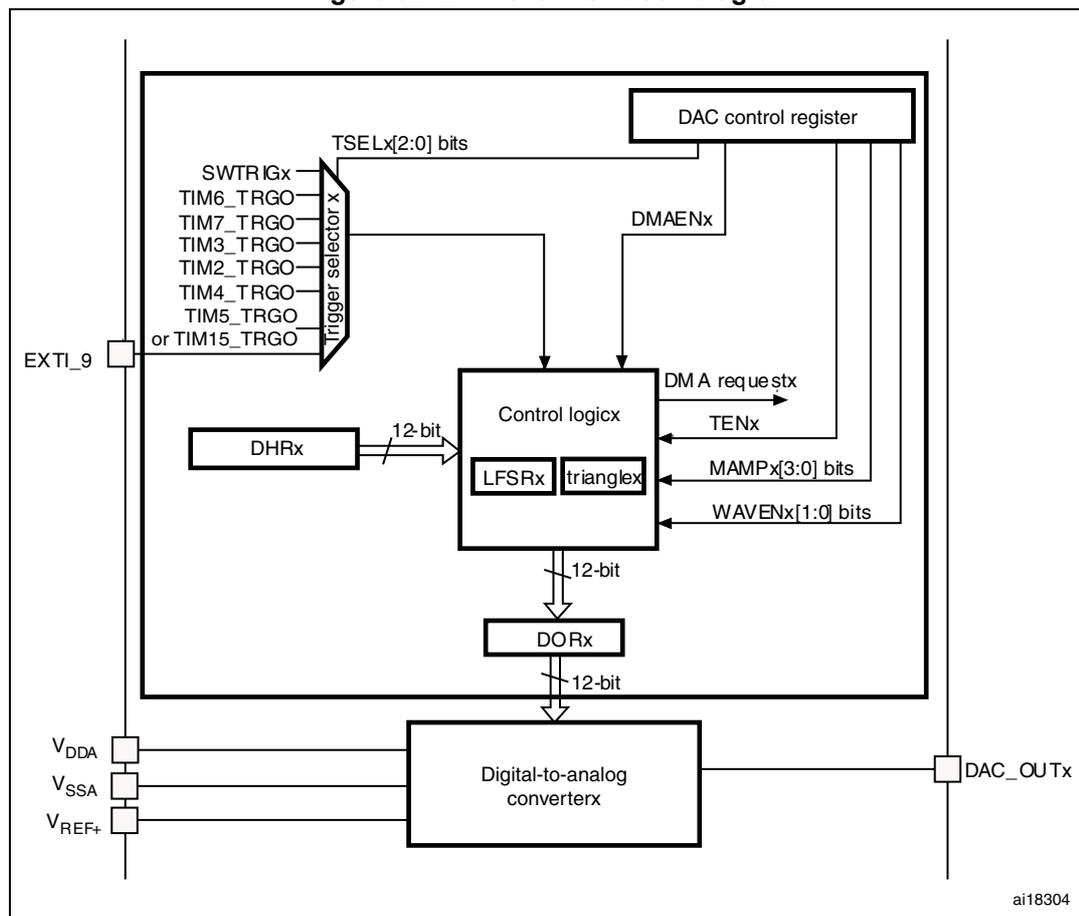
Table 63. DAC pins
| Name | Signal type | Remarks |
|---|---|---|
| V REF+ | Input, analog reference positive | The higher/positive reference voltage for the DAC, \( 2.4\text{ V} \leq V_{REF+} \leq V_{DDA} \) |
| V DDA | Input, analog supply | Analog power supply |
| V SSA | Input, analog supply ground | Ground for analog power supply |
| DAC_OUTx | Analog output signal | DAC channelx analog output |
Note: Once the DAC channelx is enabled, the corresponding GPIO pin (PA4 or PA5) is automatically connected to the analog converter output (DAC_OUTx). In order to avoid parasitic consumption, the PA4 or PA5 pin should first be configured to analog (AIN).
11.3 DAC functional description
11.3.1 DAC channel enable
Each DAC channel can be powered on by setting its corresponding ENx bit in the DAC_CR register. The DAC channel is then enabled after a startup time \( t_{\text{WAKEUP}} \) .
Note: The ENx bit enables the analog DAC Channelx macrocell only. The DAC Channelx digital interface is enabled even if the ENx bit is reset.
11.3.2 DAC output buffer enable
The DAC integrates two output buffers that can be used to reduce the output impedance, and to drive external loads directly without having to add an external operational amplifier. Each DAC channel output buffer can be enabled and disabled using the corresponding BOFFx bit in the DAC_CR register.
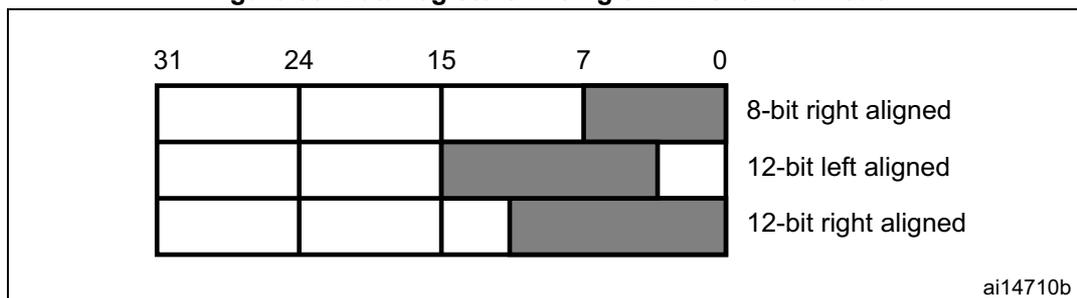
11.3.3 DAC data format
Depending on the selected configuration mode, the data have to be written into the specified register as described below:
- • Single DAC channelx, there are three possibilities:
- – 8-bit right alignment: the software has to load data into the DAC_DHR8Rx [7:0] bits (stored into the DHRx[11:4] bits)
- – 12-bit left alignment: the software has to load data into the DAC_DHR12Lx [15:4] bits (stored into the DHRx[11:0] bits)
- – 12-bit right alignment: the software has to load data into the DAC_DHR12Rx [11:0] bits (stored into the DHRx[11:0] bits)
Depending on the loaded DAC_DHRyyxx register, the data written by the user is shifted and stored into the corresponding DHRx (data holding registerx, which are internal non-memory-mapped registers). The DHRx register is then loaded into the DORx register either automatically, by software trigger or by an external event trigger.
Figure 33. Data registers in single DAC channel mode
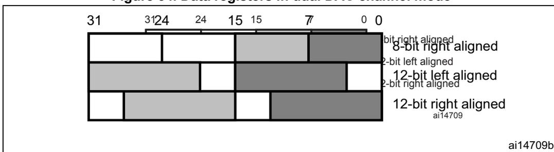
- • Dual DAC channels, there are three possibilities:
- – 8-bit right alignment: data for DAC channel1 to be loaded into the DAC_DHR8RD [7:0] bits (stored into the DHR1[11:4] bits) and data for DAC channel2 to be loaded into the DAC_DHR8RD [15:8] bits (stored into the DHR2[11:4] bits)
- – 12-bit left alignment: data for DAC channel1 to be loaded into the DAC_DHR12LD [15:4] bits (stored into the DHR1[11:0] bits) and data for DAC channel2 to be loaded into the DAC_DHR12LD [31:20] bits (stored into the DHR2[11:0] bits)
- – 12-bit right alignment: data for DAC channel1 to be loaded into the DAC_DHR12RD [11:0] bits (stored into the DHR1[11:0] bits) and data for DAC channel2 to be loaded into the DAC_DHR12LD [27:16] bits (stored into the DHR2[11:0] bits)
Depending on the loaded DAC_DHRyyD register, the data written by the user is shifted and stored into DHR1 and DHR2 (data holding registers, which are internal non-memory-mapped registers). The DHR1 and DHR2 registers are then loaded into the DOR1 and DOR2 registers, respectively, either automatically, by software trigger or by an external event trigger.
Figure 34. Data registers in dual DAC channel mode
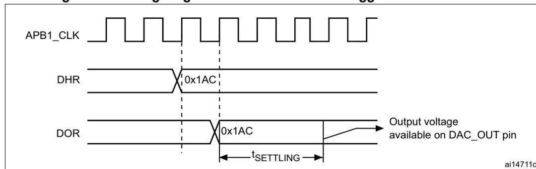
11.3.4 DAC conversion
The DAC_DORx cannot be written directly and any data transfer to the DAC channelx must be performed by loading the DAC_DHRx register (write to DAC_DHR8Rx, DAC_DHR12Lx, DAC_DHR12Rx, DAC_DHR8RD, DAC_DHR12LD or DAC_DHR12LD).
Data stored in the DAC_DHRx register are automatically transferred to the DAC_DORx register after one APB1 clock cycle, if no hardware trigger is selected (TENx bit in DAC_CR register is reset). However, when a hardware trigger is selected (TENx bit in DAC_CR register is set) and a trigger occurs, the transfer is performed three APB1 clock cycles later.
When DAC_DORx is loaded with the DAC_DHRx contents, the analog output voltage becomes available after a time \( t_{\text{SETTLING}} \) that depends on the power supply voltage and the analog output load.
Figure 35. Timing diagram for conversion with trigger disabled TEN = 0
11.3.5 DAC output voltage
Digital inputs are converted to output voltages on a linear conversion between 0 and \( V_{\text{REF+}} \) . The analog output voltages on each DAC channel pin are determined by the following equation:
11.3.6 DAC trigger selection
If the TENx control bit is set, conversion can then be triggered by an external event (timer counter, external interrupt line). The TSELx[2:0] control bits determine which out of eight possible events trigger conversion as shown in Table 64 .
Table 64. External triggers
| Source | Type | TSEL[2:0] |
|---|---|---|
| Timer 6 TRGO event | Internal signal from on-chip timers | 000 |
| Timer 3 TRGO event | 001 | |
| Timer 7 TRGO event | 010 | |
| Timer 5 or Timer 15 TRGO event | 011 | |
| Timer 2 TRGO event | 100 | |
| Timer 4 TRGO event | 101 | |
| EXTI line9 | External pin | 110 |
| SWTRIG | Software control bit | 111 |
Each time a DAC interface detects a rising edge on the selected timer TRGO output, or on the selected external interrupt line 9, the last data stored into the DAC_DHRx register are transferred into the DAC_DORx register. The DAC_DORx register is updated three APB1 cycles after the trigger occurs.
If the software trigger is selected, the conversion starts once the SWTRIG bit is set. SWTRIG is reset by hardware once the DAC_DORx register has been loaded with the DAC_DHRx register contents.
Note: TSELx[2:0] bit cannot be changed when the ENx bit is set.
When software trigger is selected, the transfer from the DAC_DHRx register to the DAC_DORx register takes only one APB1 clock cycle.
For High-density value line devices, the TIM15 TRGO event is selected as DAC Trigger 3 only if the MISC_REMAP bit in the AFIO_MAPR2 register is set and DAC Trigger 3 is connected to TIM5 TRGO when the MISC_REMAP bit in the AFIO_MAPR2 register is reset. On low- and medium-density devices the TIM15 TRGO event is always selected as DAC Trigger 3. For more details refer to the Section 7.3: Alternate function I/O and debug configuration (AFIO) on page 117 .
11.3.7 DMA request
Each DAC channel has a DMA capability. Two DMA channels are used to service DAC channel DMA requests.
A DAC DMA request is generated when an external trigger (but not a software trigger) occurs while the DMAENx bit is set. The value of the DAC_DHRx register is then transferred into the DAC_DORx register.
In dual mode, if both DMAENx bits are set, two DMA requests are generated. If only one DMA request is needed, the user should set only the corresponding DMAENx bit. In this way, the application can manage both DAC channels in dual mode by using one DMA request and a unique DMA channel.
DMA underrun
The DAC DMA request is not queued so that if a second external trigger arrives before the acknowledgement for the first external trigger is received (first request), then no new request is issued and the DMA channelx underrun flag DMAUDRx in the DAC_SR register is set, reporting the error condition. DMA data transfers are then disabled and no further DMA request is treated. The DAC channelx continues to convert old data.
The software should clear the DMAUDRx flag by writing “1”, clear the DMAEN bit of the used DMA stream and re-initialize both DMA and DAC channelx to restart the transfer correctly. The software should modify the DAC trigger conversion frequency or lighten the DMA workload to avoid a new DMA underrun. Finally, the DAC conversion could be resumed by enabling both DMA data transfer and conversion trigger.
For each DAC channelx, an interrupt is also generated if its corresponding DMAUDRIEx bit in the DAC_CR register is enabled.
11.3.8 Noise generation
In order to generate a variable-amplitude pseudonoise, an LFSR (linear feedback shift register) is available. DAC noise generation is selected by setting WAVEx[1:0] to “01”. The preloaded value in LFSR is 0xAAA. This register is updated three APB1 clock cycles after each trigger event, following a specific calculation algorithm.
Figure 36. DAC LFSR register calculation algorithm
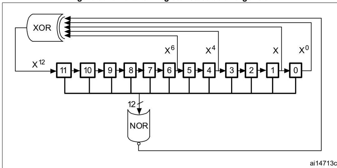
The LFSR value, that may be masked partially or totally by means of the MAMPx[3:0] bits in the DAC_CR register, is added up to the DAC_DHRx contents without overflow and this value is then stored into the DAC_DORx register.
If LFSR is 0x0000, a '1' is injected into it (antilock-up mechanism).
It is possible to reset LFSR wave generation by resetting the WAVE[1:0] bits.
Figure 37. DAC conversion (SW trigger enabled) with LFSR wave generation
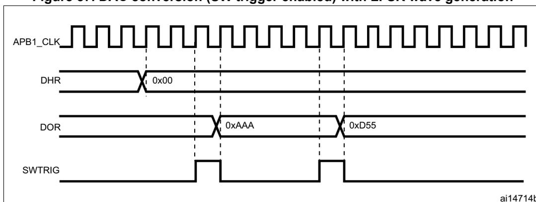
Note: The DAC trigger must be enabled for noise generation by setting the TENx bit in the DAC_CR register.
11.3.9 Triangle-wave generation
It is possible to add a small-amplitude triangular waveform on a DC or slowly varying signal. DAC triangle-wave generation is selected by setting WAVE[1:0] to "10". The amplitude is configured through the MAMPx[3:0] bits in the DAC_CR register. An internal triangle counter is incremented three APB1 clock cycles after each trigger event. The value of this counter is then added to the DAC_DHRx register without overflow and the sum is stored into the DAC_DORx register. The triangle counter is incremented as long as it is less than the maximum amplitude defined by the MAMPx[3:0] bits. Once the configured amplitude is reached, the counter is decremented down to 0, then incremented again and so on.
It is possible to reset triangle wave generation by resetting the WAVEx[1:0] bits.
Figure 38. DAC triangle wave generation
![Figure 38: DAC triangle wave generation graph. The y-axis shows 'MAMPx[3:0] max amplitude + DAC_DHRx base value' at the top and 'DAC_DHRx base value' at the bottom. The x-axis represents time. The graph shows a triangle wave starting at the base value, rising linearly (labeled 'Incrementation'), reaching the maximum amplitude, falling linearly (labeled 'Decrementation'), and returning to the base value. The wave then repeats. The label 'ai14715c' is in the bottom right corner.](/RM0041-STM32F100/1fd19b7548b34d7d344b9be32b639deb_img.jpg)
Figure 39. DAC conversion (SW trigger enabled) with triangle wave generation
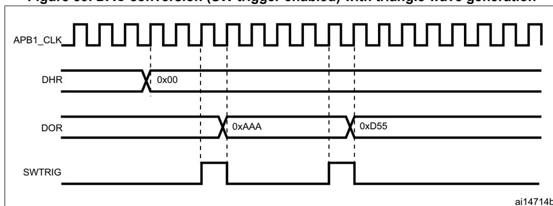
Note: The DAC trigger must be enabled for noise generation by setting the TENx bit in the DAC_CR register.
The MAMPx[3:0] bits must be configured before enabling the DAC, otherwise they cannot be changed.
11.4 Dual DAC channel conversion
To efficiently use the bus bandwidth in applications that require the two DAC channels at the same time, three dual registers are implemented: DHR8RD, DHR12RD and DHR12LD. A unique register access is then required to drive both DAC channels at the same time.
Eleven possible conversion modes are possible using the two DAC channels and these dual registers. All the conversion modes can nevertheless be obtained using separate DHRx registers if needed.
All modes are described in the paragraphs below.
11.4.1 Independent trigger without wave generation
To configure the DAC in this conversion mode, the following sequence is required:
- • Set the two DAC channel trigger enable bits TEN1 and TEN2
- • Configure different trigger sources by setting different values in the TSEL1[2:0] and TSEL2[2:0] bits
- • Load the dual DAC channel data into the desired DHR register (DAC_DHR12RD, DAC_DHR12LD or DAC_DHR8RD)
When a DAC channel1 trigger arrives, the DHR1 register is transferred into DAC_DOR1 (three APB1 clock cycles later).
When a DAC channel2 trigger arrives, the DHR2 register is transferred into DAC_DOR2 (three APB1 clock cycles later).
11.4.2 Independent trigger with single LFSR generation
To configure the DAC in this conversion mode, the following sequence is required:
- • Set the two DAC channel trigger enable bits TEN1 and TEN2
- • Configure different trigger sources by setting different values in the TSEL1[2:0] and TSEL2[2:0] bits
- • Configure the two DAC channel WAVEx[1:0] bits as “01” and the same LFSR mask value in the MAMPx[3:0] bits
- • Load the dual DAC channel data into the desired DHR register (DHR12RD, DHR12LD or DHR8RD)
When a DAC channel1 trigger arrives, the LFSR1 counter, with the same mask, is added to the DHR1 register and the sum is transferred into DAC_DOR1 (three APB1 clock cycles later). Then the LFSR1 counter is updated.
When a DAC channel2 trigger arrives, the LFSR2 counter, with the same mask, is added to the DHR2 register and the sum is transferred into DAC_DOR2 (three APB1 clock cycles later). Then the LFSR2 counter is updated.
11.4.3 Independent trigger with different LFSR generation
To configure the DAC in this conversion mode, the following sequence is required:
- • Set the two DAC channel trigger enable bits TEN1 and TEN2
- • Configure different trigger sources by setting different values in the TSEL1[2:0] and TSEL2[2:0] bits
- • Configure the two DAC channel WAVEx[1:0] bits as “01” and set different LFSR masks values in the MAMP1[3:0] and MAMP2[3:0] bits
- • Load the dual DAC channel data into the desired DHR register (DAC_DHR12RD, DAC_DHR12LD or DAC_DHR8RD)
When a DAC channel1 trigger arrives, the LFSR1 counter, with the mask configured by MAMP1[3:0], is added to the DHR1 register and the sum is transferred into DAC_DOR1 (three APB1 clock cycles later). Then the LFSR1 counter is updated.
When a DAC channel2 trigger arrives, the LFSR2 counter, with the mask configured by MAMP2[3:0], is added to the DHR2 register and the sum is transferred into DAC_DOR2 (three APB1 clock cycles later). Then the LFSR2 counter is updated.
11.4.4 Independent trigger with single triangle generation
To configure the DAC in this conversion mode, the following sequence is required:
- • Set the two DAC channel trigger enable bits TEN1 and TEN2
- • Configure different trigger sources by setting different values in the TSEL1[2:0] and TSEL2[2:0] bits
- • Configure the two DAC channel WAVEx[1:0] bits as “1x” and the same maximum amplitude value in the MAMPx[3:0] bits
- • Load the dual DAC channel data into the desired DHR register (DAC_DHR12RD, DAC_DHR12LD or DAC_DHR8RD)
When a DAC channel1 trigger arrives, the DAC channel1 triangle counter, with the same triangle amplitude, is added to the DHR1 register and the sum is transferred into DAC_DOR1 (three APB1 clock cycles later). The DAC channel1 triangle counter is then updated.
When a DAC channel2 trigger arrives, the DAC channel2 triangle counter, with the same triangle amplitude, is added to the DHR2 register and the sum is transferred into DAC_DOR2 (three APB1 clock cycles later). The DAC channel2 triangle counter is then updated.
11.4.5 Independent trigger with different triangle generation
To configure the DAC in this conversion mode, the following sequence is required:
- • Set the two DAC channel trigger enable bits TEN1 and TEN2
- • Configure different trigger sources by setting different values in the TSEL1[2:0] and TSEL2[2:0] bits
- • Configure the two DAC channel WAVEx[1:0] bits as “1x” and set different maximum amplitude values in the MAMP1[3:0] and MAMP2[3:0] bits
- • Load the dual DAC channel data into the desired DHR register (DAC_DHR12RD, DAC_DHR12LD or DAC_DHR8RD)
When a DAC channel1 trigger arrives, the DAC channel1 triangle counter, with a triangle amplitude configured by MAMP1[3:0], is added to the DHR1 register and the sum is transferred into DAC_DOR1 (three APB1 clock cycles later). The DAC channel1 triangle counter is then updated.
When a DAC channel2 trigger arrives, the DAC channel2 triangle counter, with a triangle amplitude configured by MAMP2[3:0], is added to the DHR2 register and the sum is transferred into DAC_DOR2 (three APB1 clock cycles later). The DAC channel2 triangle counter is then updated.
11.4.6 Simultaneous software start
To configure the DAC in this conversion mode, the following sequence is required:
- • Load the dual DAC channel data to the desired DHR register (DAC_DHR12RD, DAC_DHR12LD or DAC_DHR8RD)
In this configuration, one APB1 clock cycle later, the DHR1 and DHR2 registers are transferred into DAC_DOR1 and DAC_DOR2, respectively.
11.4.7 Simultaneous trigger without wave generation
To configure the DAC in this conversion mode, the following sequence is required:
- • Set the two DAC channel trigger enable bits TEN1 and TEN2
- • Configure the same trigger source for both DAC channels by setting the same value in the TSEL1[2:0] and TSEL2[2:0] bits
- • Load the dual DAC channel data to the desired DHR register (DAC_DHR12RD, DAC_DHR12LD or DAC_DHR8RD)
When a trigger arrives, the DHR1 and DHR2 registers are transferred into DAC_DOR1 and DAC_DOR2, respectively (after three APB1 clock cycles).
11.4.8 Simultaneous trigger with single LFSR generation
To configure the DAC in this conversion mode, the following sequence is required:
- • Set the two DAC channel trigger enable bits TEN1 and TEN2
- • Configure the same trigger source for both DAC channels by setting the same value in the TSEL1[2:0] and TSEL2[2:0] bits
- • Configure the two DAC channel WAVEx[1:0] bits as “01” and the same LFSR mask value in the MAMPx[3:0] bits
- • Load the dual DAC channel data to the desired DHR register (DHR12RD, DHR12LD or DHR8RD)
When a trigger arrives, the LFSR1 counter, with the same mask, is added to the DHR1 register and the sum is transferred into DAC_DOR1 (three APB1 clock cycles later). The LFSR1 counter is then updated. At the same time, the LFSR2 counter, with the same mask, is added to the DHR2 register and the sum is transferred into DAC_DOR2 (three APB1 clock cycles later). The LFSR2 counter is then updated.
11.4.9 Simultaneous trigger with different LFSR generation
To configure the DAC in this conversion mode, the following sequence is required:
- • Set the two DAC channel trigger enable bits TEN1 and TEN2
- • Configure the same trigger source for both DAC channels by setting the same value in the TSEL1[2:0] and TSEL2[2:0] bits
- • Configure the two DAC channel WAVEx[1:0] bits as “01” and set different LFSR mask values using the MAMP1[3:0] and MAMP2[3:0] bits
- • Load the dual DAC channel data into the desired DHR register (DAC_DHR12RD, DAC_DHR12LD or DAC_DHR8RD)
When a trigger arrives, the LFSR1 counter, with the mask configured by MAMP1[3:0], is added to the DHR1 register and the sum is transferred into DAC_DOR1 (three APB1 clock cycles later). The LFSR1 counter is then updated.
At the same time, the LFSR2 counter, with the mask configured by MAMP2[3:0], is added to the DHR2 register and the sum is transferred into DAC_DOR2 (three APB1 clock cycles later). The LFSR2 counter is then updated.
11.4.10 Simultaneous trigger with single triangle generation
To configure the DAC in this conversion mode, the following sequence is required:
- • Set the two DAC channel trigger enable bits TEN1 and TEN2
- • Configure the same trigger source for both DAC channels by setting the same value in the TSEL1[2:0] and TSEL2[2:0] bits
- • Configure the two DAC channel WAVEx[1:0] bits as “1x” and the same maximum amplitude value using the MAMPx[3:0] bits
- • Load the dual DAC channel data into the desired DHR register (DAC_DHR12RD, DAC_DHR12LD or DAC_DHR8RD)
When a trigger arrives, the DAC channel1 triangle counter, with the same triangle amplitude, is added to the DHR1 register and the sum is transferred into DAC_DOR1 (three APB1 clock cycles later). The DAC channel1 triangle counter is then updated.
At the same time, the DAC channel2 triangle counter, with the same triangle amplitude, is added to the DHR2 register and the sum is transferred into DAC_DOR2 (three APB1 clock cycles later). The DAC channel2 triangle counter is then updated.
11.4.11 Simultaneous trigger with different triangle generation
To configure the DAC in this conversion mode, the following sequence is required:
- • Set the two DAC channel trigger enable bits TEN1 and TEN2
- • Configure the same trigger source for both DAC channels by setting the same value in the TSEL1[2:0] and TSEL2[2:0] bits
- • Configure the two DAC channel WAVEx[1:0] bits as “1x” and set different maximum amplitude values in the MAMP1[3:0] and MAMP2[3:0] bits
- • Load the dual DAC channel data into the desired DHR register (DAC_DHR12RD, DAC_DHR12LD or DAC_DHR8RD)
When a trigger arrives, the DAC channel1 triangle counter, with a triangle amplitude configured by MAMP1[3:0], is added to the DHR1 register and the sum is transferred into DAC_DOR1 (three APB1 clock cycles later). Then the DAC channel1 triangle counter is updated.
At the same time, the DAC channel2 triangle counter, with a triangle amplitude configured by MAMP2[3:0], is added to the DHR2 register and the sum is transferred into DAC_DOR2 (three APB1 clock cycles later). Then the DAC channel2 triangle counter is updated.
11.5 DAC registers
Refer to Section 1.1: List of abbreviations for registers for registers for a list of abbreviations used in register descriptions.
The peripheral registers have to be accessed by words (32 bits).
11.5.1 DAC control register (DAC_CR)
Address offset: 0x00
Reset value: 0x0000 0000
| 31 | 30 | 29 | 28 | 27 | 26 | 25 | 24 | 23 | 22 | 21 | 20 | 19 | 18 | 17 | 16 |
|---|---|---|---|---|---|---|---|---|---|---|---|---|---|---|---|
| Reserved | DMAU DRIE2 | DMA EN2 | MAMP2[3:0] | WAVE2[1:0] | TSEL2[2:0] | TEN2 | BOFF2 | EN2 | |||||||
| rw | rw | rw | rw | rw | rw | rw | rw | rw | rw | rw | rw | rw | rw | ||
| 15 | 14 | 13 | 12 | 11 | 10 | 9 | 8 | 7 | 6 | 5 | 4 | 3 | 2 | 1 | 0 |
| Reserved | DMAU DRIE1 | DMA EN1 | MAMP1[3:0] | WAVE1[1:0] | TSEL1[2:0] | TEN1 | BOFF1 | EN1 | |||||||
| rw | rw | rw | rw | rw | rw | rw | rw | rw | rw | rw | rw | rw | rw | ||
Bits 31:30 Reserved, must be kept at reset value.
Bits 29 DMAUDRIE2 : DAC channel2 DMA underrun interrupt enable
This bit is set and cleared by software.
0: DAC channel2 DMA underrun interrupt disabled
1: DAC channel2 DMA underrun interrupt enabled
Bit 28 DMAEN2 : DAC channel2 DMA enable
This bit is set and cleared by software.
0: DAC channel2 DMA mode disabled
1: DAC channel2 DMA mode enabled
Bits 27:24 MAMP2[3:0] : DAC channel2 mask/amplitude selector
These bits are written by software to select mask in wave generation mode or amplitude in triangle generation mode.
0000: Unmask bit0 of LFSR/ triangle amplitude equal to 1
0001: Unmask bits[1:0] of LFSR/ triangle amplitude equal to 3
0010: Unmask bits[2:0] of LFSR/ triangle amplitude equal to 7
0011: Unmask bits[3:0] of LFSR/ triangle amplitude equal to 15
0100: Unmask bits[4:0] of LFSR/ triangle amplitude equal to 31
0101: Unmask bits[5:0] of LFSR/ triangle amplitude equal to 63
0110: Unmask bits[6:0] of LFSR/ triangle amplitude equal to 127
0111: Unmask bits[7:0] of LFSR/ triangle amplitude equal to 255
1000: Unmask bits[8:0] of LFSR/ triangle amplitude equal to 511
1001: Unmask bits[9:0] of LFSR/ triangle amplitude equal to 1023
1010: Unmask bits[10:0] of LFSR/ triangle amplitude equal to 2047
≥ 1011: Unmask bits[11:0] of LFSR/ triangle amplitude equal to 4095
Bits 23:22 WAVE2[1:0] : DAC channel2 noise/triangle wave generation enable
These bits are set/reset by software.
00: wave generation disabled
01: Noise wave generation enabled
1x: Triangle wave generation enabled
Note: Only used if bit TEN2 = 1 (DAC channel2 trigger enabled)
Bits 21:19 tsel2[2:0] : DAC channel2 trigger selection
These bits select the external event used to trigger DAC channel2
000: Timer 6 TRGO event
001: Timer 3 TRGO event
010: Timer 7 TRGO event
011: Timer 5 or timer 15 TRGO event
100: Timer 2 TRGO event
101: Timer 4 TRGO event
110: External line9
111: Software trigger
Note: Only used if bit TEN2 = 1 (DAC channel2 trigger enabled).
For high-density value line devices, the TIM15 TRGO event is selected as DAC Trigger 3 only if the MISC_REMAP bit in the AFIO_MAPR2 register is set and DAC Trigger 3 is connected to TIM5 TRGO when the MISC_REMAP bit in the AFIO_MAPR2 register is reset. On low- and medium-density devices the TIM15 TRGO event is always selected as DAC Trigger 3. For more details refer to the AFIO section.
Bit 18 TEN2 : DAC channel2 trigger enable
This bit is set and cleared by software to enable/disable DAC channel2 trigger
0: DAC channel2 trigger disabled and data written into the DAC_DHRx register are transferred one APB1 clock cycle later to the DAC_DOR2 register
1: DAC channel2 trigger enabled and data from the DAC_DHRx register are transferred three APB1 clock cycles later to the DAC_DOR2 register
Note: When software trigger is selected, the transfer from the DAC_DHRx register to the DAC_DOR2 register takes only one APB1 clock cycle.
Bit 17 BOFF2 : DAC channel2 output buffer disable
This bit is set and cleared by software to enable/disable DAC channel2 output buffer.
0: DAC channel2 output buffer enabled
1: DAC channel2 output buffer disabled
Bit 16 EN2 : DAC channel2 enable
This bit is set and cleared by software to enable/disable DAC channel2.
0: DAC channel2 disabled
1: DAC channel2 enabled
Bits 15:14 Reserved, must be kept at reset value.
Bit 13 DMAUDRIE1 : DAC channel1 DMA Underrun Interrupt enable
This bit is set and cleared by software.
0: DAC channel1 DMA Underrun Interrupt disabled
1: DAC channel1 DMA Underrun Interrupt enabled
Bit 12 DMAEN1 : DAC channel1 DMA enable
This bit is set and cleared by software.
0: DAC channel1 DMA mode disabled
1: DAC channel1 DMA mode enabled
Bits 11:8 MAMP1[3:0]: DAC channel1 mask/amplitude selectorThese bits are written by software to select mask in wave generation mode or amplitude in triangle generation mode.
0000: Unmask bit0 of LFSR/ triangle amplitude equal to 1
0001: Unmask bits[1:0] of LFSR/ triangle amplitude equal to 3
0010: Unmask bits[2:0] of LFSR/ triangle amplitude equal to 7
0011: Unmask bits[3:0] of LFSR/ triangle amplitude equal to 15
0100: Unmask bits[4:0] of LFSR/ triangle amplitude equal to 31
0101: Unmask bits[5:0] of LFSR/ triangle amplitude equal to 63
0110: Unmask bits[6:0] of LFSR/ triangle amplitude equal to 127
0111: Unmask bits[7:0] of LFSR/ triangle amplitude equal to 255
1000: Unmask bits[8:0] of LFSR/ triangle amplitude equal to 511
1001: Unmask bits[9:0] of LFSR/ triangle amplitude equal to 1023
1010: Unmask bits[10:0] of LFSR/ triangle amplitude equal to 2047
≥ 1011: Unmask bits[11:0] of LFSR/ triangle amplitude equal to 4095
Bits 7:6 WAVE1[1:0]: DAC channel1 noise/triangle wave generation enableThese bits are set and cleared by software.
00: wave generation disabled
01: Noise wave generation enabled
1x: Triangle wave generation enabled
Note: Only used if bit TEN1 = 1 (DAC channel1 trigger enabled).
Bits 5:3 TSEL1[2:0]: DAC channel1 trigger selectionThese bits select the external event used to trigger DAC channel1.
000: Timer 6 TRGO event
001: Timer 3 TRGO event
010: Timer 7 TRGO event
011: Timer 5 or Timer 15 TRGO event
100: Timer 2 TRGO event
101: Timer 4 TRGO event
110: External line9
111: Software trigger
Note: Only used if bit TEN1 = 1 (DAC channel1 trigger enabled).
Bit 2 TEN1: DAC channel1 trigger enableThis bit is set and cleared by software to enable/disable DAC channel1 trigger.
0: DAC channel1 trigger disabled and data written into the DAC_DHRx register are transferred one APB1 clock cycle later to the DAC_DOR1 register
1: DAC channel1 trigger enabled and data from the DAC_DHRx register are transferred three APB1 clock cycles later to the DAC_DOR1 register
Note: When software trigger is selected, the transfer from the DAC_DHRx register to the DAC_DOR1 register takes only one APB1 clock cycle.
Bit 1 BOFF1: DAC channel1 output buffer disableThis bit is set and cleared by software to enable/disable DAC channel1 output buffer.
0: DAC channel1 output buffer enabled
1: DAC channel1 output buffer disabled
Bit 0 EN1: DAC channel1 enableThis bit is set and cleared by software to enable/disable DAC channel1.
0: DAC channel1 disabled
1: DAC channel1 enabled
11.5.2 DAC software trigger register (DAC_SWTRIGR)
Address offset: 0x04
Reset value: 0x0000 0000
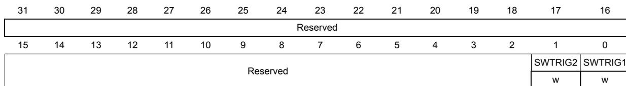
| 31 | 30 | 29 | 28 | 27 | 26 | 25 | 24 | 23 | 22 | 21 | 20 | 19 | 18 | 17 | 16 |
| Reserved | |||||||||||||||
| 15 | 14 | 13 | 12 | 11 | 10 | 9 | 8 | 7 | 6 | 5 | 4 | 3 | 2 | 1 | 0 |
| Reserved | SWTRIG2 | SWTRIG1 | |||||||||||||
| w | w | ||||||||||||||
Bits 31:2 Reserved, must be kept at reset value.
Bit 1 SWTRIG2 : DAC channel2 software trigger
This bit is set and cleared by software to enable/disable the software trigger.
0: Software trigger disabled
1: Software trigger enabled
Note: This bit is cleared by hardware (one APB1 clock cycle later) once the DAC_DHR2 register value has been loaded into the DAC_DOR2 register.
Bit 0 SWTRIG1 : DAC channel1 software trigger
This bit is set and cleared by software to enable/disable the software trigger.
0: Software trigger disabled
1: Software trigger enabled
Note: This bit is cleared by hardware (one APB1 clock cycle later) once the DAC_DHR1 register value has been loaded into the DAC_DOR1 register.
11.5.3 DAC channel1 12-bit right-aligned data holding register (DAC_DHR12R1)
Address offset: 0x08
Reset value: 0x0000 0000
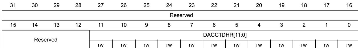
| 31 | 30 | 29 | 28 | 27 | 26 | 25 | 24 | 23 | 22 | 21 | 20 | 19 | 18 | 17 | 16 |
| Reserved | |||||||||||||||
| 15 | 14 | 13 | 12 | 11 | 10 | 9 | 8 | 7 | 6 | 5 | 4 | 3 | 2 | 1 | 0 |
| Reserved | DACC1DHR[11:0] | ||||||||||||||
| rw | rw | rw | rw | rw | rw | rw | rw | rw | rw | rw | rw | ||||
Bits 31:12 Reserved, must be kept at reset value.
Bits 11:0 DACC1DHR[11:0] : DAC channel1 12-bit right-aligned data
These bits are written by software which specifies 12-bit data for DAC channel1.
11.5.4 DAC channel1 12-bit left aligned data holding register (DAC_DHR12L1)
Address offset: 0x0C
Reset value: 0x0000 0000
| 31 | 30 | 29 | 28 | 27 | 26 | 25 | 24 | 23 | 22 | 21 | 20 | 19 | 18 | 17 | 16 |
|---|---|---|---|---|---|---|---|---|---|---|---|---|---|---|---|
| Reserved | |||||||||||||||
| 15 | 14 | 13 | 12 | 11 | 10 | 9 | 8 | 7 | 6 | 5 | 4 | 3 | 2 | 1 | 0 |
| DACC1DHR[11:0] | Reserved | ||||||||||||||
| rw | rw | rw | rw | rw | rw | rw | rw | rw | rw | rw | rw | ||||
Bits 31:16 Reserved, must be kept at reset value.
Bits 15:4 DACC1DHR[11:0] : DAC channel1 12-bit left-aligned data
These bits are written by software which specifies 12-bit data for DAC channel1.
Bits 3:0 Reserved, must be kept at reset value.
11.5.5 DAC channel1 8-bit right aligned data holding register (DAC_DHR8R1)
Address offset: 0x10
Reset value: 0x0000 0000
| 31 | 30 | 29 | 28 | 27 | 26 | 25 | 24 | 23 | 22 | 21 | 20 | 19 | 18 | 17 | 16 |
|---|---|---|---|---|---|---|---|---|---|---|---|---|---|---|---|
| Reserved | |||||||||||||||
| 15 | 14 | 13 | 12 | 11 | 10 | 9 | 8 | 7 | 6 | 5 | 4 | 3 | 2 | 1 | 0 |
| Reserved | DACC1DHR[7:0] | ||||||||||||||
| rw | rw | rw | rw | rw | rw | rw | rw | ||||||||
Bits 31:8 Reserved, must be kept at reset value.
Bits 7:0 DACC1DHR[7:0] : DAC channel1 8-bit right-aligned data
These bits are written by software which specifies 8-bit data for DAC channel1.
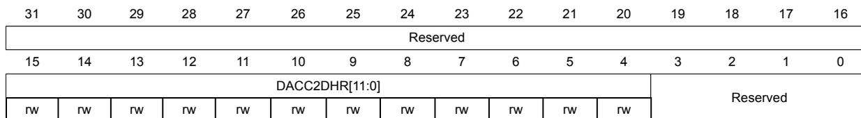
11.5.6 DAC channel2 12-bit right aligned data holding register (DAC_DHR12R2)
Address offset: 0x14
Reset value: 0x0000 0000

| 31 | 30 | 29 | 28 | 27 | 26 | 25 | 24 | 23 | 22 | 21 | 20 | 19 | 18 | 17 | 16 |
| Reserved | |||||||||||||||
| 15 | 14 | 13 | 12 | 11 | 10 | 9 | 8 | 7 | 6 | 5 | 4 | 3 | 2 | 1 | 0 |
| Reserved | DACC2DHR[11:0] | ||||||||||||||
| rw | rw | rw | rw | rw | rw | rw | rw | rw | rw | rw | rw | ||||
Bits 31:12 Reserved, must be kept at reset value.
Bits 11:0 DACC2DHR[11:0] : DAC channel2 12-bit right-aligned data
These bits are written by software which specifies 12-bit data for DAC channel2.
11.5.7 DAC channel2 12-bit left aligned data holding register (DAC_DHR12L2)
Address offset: 0x18
Reset value: 0x0000 0000
| 31 | 30 | 29 | 28 | 27 | 26 | 25 | 24 | 23 | 22 | 21 | 20 | 19 | 18 | 17 | 16 |
| Reserved | |||||||||||||||
| 15 | 14 | 13 | 12 | 11 | 10 | 9 | 8 | 7 | 6 | 5 | 4 | 3 | 2 | 1 | 0 |
| DACC2DHR[11:0] | Reserved | ||||||||||||||
| rw | rw | rw | rw | rw | rw | rw | rw | rw | rw | rw | rw | ||||
Bits 31:16 Reserved, must be kept at reset value.
Bits 15:4 DACC2DHR[11:0] : DAC channel2 12-bit left-aligned data
These bits are written by software which specify 12-bit data for DAC channel2.
Bits 3:0 Reserved, must be kept at reset value.
11.5.8 DAC channel2 8-bit right-aligned data holding register (DAC_DHR8R2)
Address offset: 0x1C
Reset value: 0x0000 0000
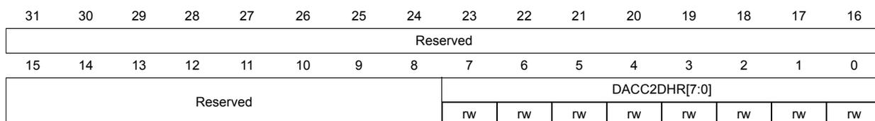
| 31 | 30 | 29 | 28 | 27 | 26 | 25 | 24 | 23 | 22 | 21 | 20 | 19 | 18 | 17 | 16 |
| Reserved | |||||||||||||||
| 15 | 14 | 13 | 12 | 11 | 10 | 9 | 8 | 7 | 6 | 5 | 4 | 3 | 2 | 1 | 0 |
| Reserved | DACC2DHR[7:0] | ||||||||||||||
| rw | rw | rw | rw | rw | rw | rw | rw | ||||||||
Bits 31:8 Reserved, must be kept at reset value.
Bits 7:0 DACC2DHR[7:0] : DAC channel2 8-bit right-aligned data
These bits are written by software which specifies 8-bit data for DAC channel2.
11.5.9 Dual DAC 12-bit right-aligned data holding register (DAC_DHR12RD)
Address offset: 0x20
Reset value: 0x0000 0000
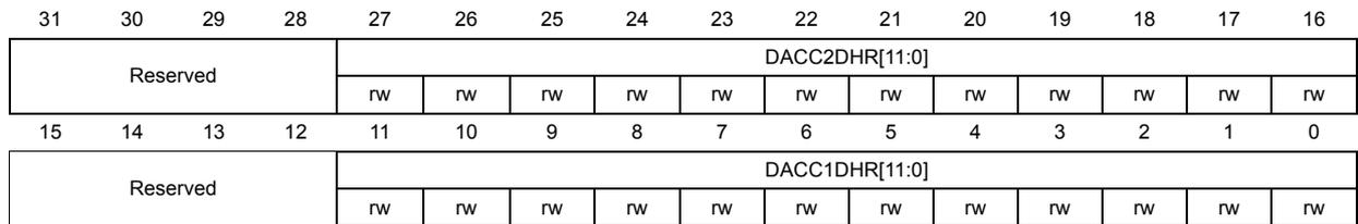
| 31 | 30 | 29 | 28 | 27 | 26 | 25 | 24 | 23 | 22 | 21 | 20 | 19 | 18 | 17 | 16 |
| Reserved | DACC2DHR[11:0] | ||||||||||||||
| rw | rw | rw | rw | rw | rw | rw | rw | rw | rw | rw | rw | ||||
| 15 | 14 | 13 | 12 | 11 | 10 | 9 | 8 | 7 | 6 | 5 | 4 | 3 | 2 | 1 | 0 |
| Reserved | DACC1DHR[11:0] | ||||||||||||||
| rw | rw | rw | rw | rw | rw | rw | rw | rw | rw | rw | rw | ||||
Bits 31:28 Reserved, must be kept at reset value.
Bits 27:16 DACC2DHR[11:0] : DAC channel2 12-bit right-aligned data
These bits are written by software which specifies 12-bit data for DAC channel2.
Bits 15:12 Reserved, must be kept at reset value.
Bits 11:0 DACC1DHR[11:0] : DAC channel1 12-bit right-aligned data
These bits are written by software which specifies 12-bit data for DAC channel1.
11.5.10 DUAL DAC 12-bit left aligned data holding register (DAC_DHR12LD)
Address offset: 0x24
Reset value: 0x0000 0000
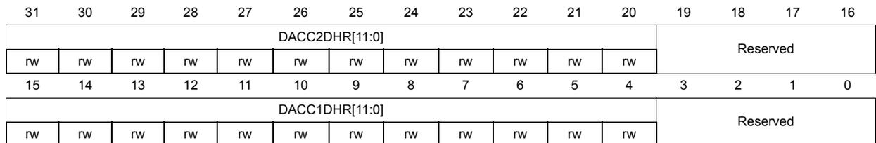
| 31 | 30 | 29 | 28 | 27 | 26 | 25 | 24 | 23 | 22 | 21 | 20 | 19 | 18 | 17 | 16 |
| DACC2DHR[11:0] | Reserved | ||||||||||||||
| rw | rw | rw | rw | rw | rw | rw | rw | rw | rw | rw | rw | ||||
| 15 | 14 | 13 | 12 | 11 | 10 | 9 | 8 | 7 | 6 | 5 | 4 | 3 | 2 | 1 | 0 |
| DACC1DHR[11:0] | Reserved | ||||||||||||||
| rw | rw | rw | rw | rw | rw | rw | rw | rw | rw | rw | rw | ||||
Bits 31:20 DACC2DHR[11:0] : DAC channel2 12-bit left-aligned data
These bits are written by software which specifies 12-bit data for DAC channel2.
Bits 19:16 Reserved, must be kept at reset value.
Bits 15:4 DACC1DHR[11:0] : DAC channel1 12-bit left-aligned data
These bits are written by software which specifies 12-bit data for DAC channel1.
Bits 3:0 Reserved, must be kept at reset value.
11.5.11 DUAL DAC 8-bit right aligned data holding register (DAC_DHR8RD)
Address offset: 0x28
Reset value: 0x0000 0000
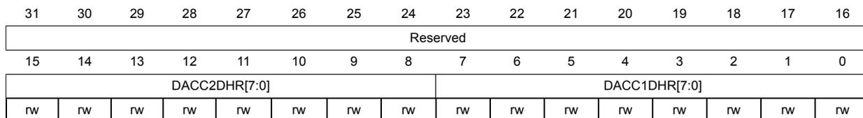
| 31 | 30 | 29 | 28 | 27 | 26 | 25 | 24 | 23 | 22 | 21 | 20 | 19 | 18 | 17 | 16 |
| Reserved | |||||||||||||||
| 15 | 14 | 13 | 12 | 11 | 10 | 9 | 8 | 7 | 6 | 5 | 4 | 3 | 2 | 1 | 0 |
| DACC2DHR[7:0] | DACC1DHR[7:0] | ||||||||||||||
| rw | rw | rw | rw | rw | rw | rw | rw | rw | rw | rw | rw | rw | rw | rw | rw |
Bits 31:16 Reserved, must be kept at reset value.
Bits 15:8 DACC2DHR[7:0] : DAC channel2 8-bit right-aligned data
These bits are written by software which specifies 8-bit data for DAC channel2.
Bits 7:0 DACC1DHR[7:0] : DAC channel1 8-bit right-aligned data
These bits are written by software which specifies 8-bit data for DAC channel1.
11.5.12 DAC channel1 data output register (DAC_DOR1)
Address offset: 0x2C
Reset value: 0x0000 0000
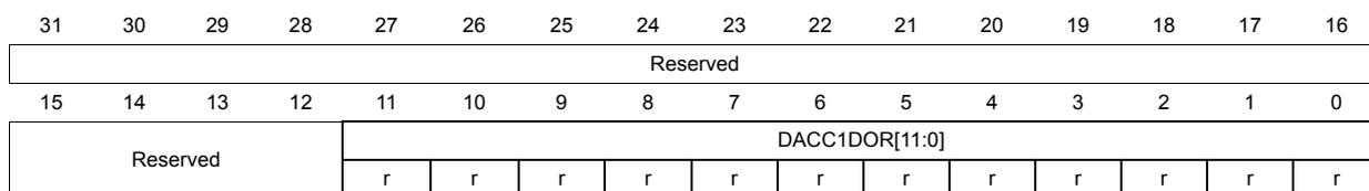
| 31 | 30 | 29 | 28 | 27 | 26 | 25 | 24 | 23 | 22 | 21 | 20 | 19 | 18 | 17 | 16 |
| Reserved | |||||||||||||||
| 15 | 14 | 13 | 12 | 11 | 10 | 9 | 8 | 7 | 6 | 5 | 4 | 3 | 2 | 1 | 0 |
| Reserved | DACC1DOR[11:0] | ||||||||||||||
| r | r | r | r | r | r | r | r | r | r | r | r | ||||
Bits 31:12 Reserved, must be kept at reset value.
Bit 11:0 DACC1DOR[11:0] : DAC channel1 data output
These bits are read-only, they contain data output for DAC channel1.
11.5.13 DAC channel2 data output register (DAC_DOR2)
Address offset: 0x30
Reset value: 0x0000 0000
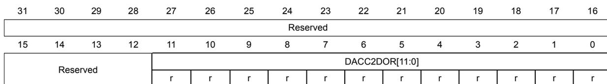
| 31 | 30 | 29 | 28 | 27 | 26 | 25 | 24 | 23 | 22 | 21 | 20 | 19 | 18 | 17 | 16 |
| Reserved | |||||||||||||||
| 15 | 14 | 13 | 12 | 11 | 10 | 9 | 8 | 7 | 6 | 5 | 4 | 3 | 2 | 1 | 0 |
| Reserved | DACC2DOR[11:0] | ||||||||||||||
| r | r | r | r | r | r | r | r | r | r | r | r | ||||
Bits 31:12 Reserved, must be kept at reset value.
Bits 11:0 DACC2DOR[11:0] : DAC channel2 data output
These bits are read-only, they contain data output for DAC channel2.
11.5.14 DAC status register (DAC_SR)
Address offset: 0x34
Reset value: 0x0000 0000
| 31 | 30 | 29 | 28 | 27 | 26 | 25 | 24 | 23 | 22 | 21 | 20 | 19 | 18 | 17 | 16 |
|---|---|---|---|---|---|---|---|---|---|---|---|---|---|---|---|
| Reserved | DMAUDR2 | Reserved | |||||||||||||
| rc_w1 | |||||||||||||||
| 15 | 14 | 13 | 12 | 11 | 10 | 9 | 8 | 7 | 6 | 5 | 4 | 3 | 2 | 1 | 0 |
| Reserved | DMAUDR1 | Reserved | |||||||||||||
| rc_w1 | |||||||||||||||
Bits 31:30 Reserved, must be kept at reset value.
Bit 29 DMAUDR2 : DAC channel2 DMA underrun flag
This bit is set by hardware and cleared by software (by writing it to 1).
0: No DMA underrun error condition occurred for DAC channel2
1: DMA underrun error condition occurred for DAC channel2 (the currently selected trigger is driving DAC channel2 conversion at a frequency higher than the DMA service capability rate)
Bits 28:14 Reserved, must be kept at reset value.
Bit 13 DMAUDR1 : DAC channel1 DMA underrun flag
This bit is set by hardware and cleared by software (by writing it to 1).
0: No DMA underrun error condition occurred for DAC channel1
1: DMA underrun error condition occurred for DAC channel1 (the currently selected trigger is driving DAC channel1 conversion at a frequency higher than the DMA service capability rate)
Bits 12:0 Reserved, must be kept at reset value.
11.5.15 DAC register map
Table 65 summarizes the DAC registers.
Table 65. DAC register map
| Offset | Register | 31 | 30 | 29 | 28 | 27 | 26 | 25 | 24 | 23 | 22 | 21 | 20 | 19 | 18 | 17 | 16 | 15 | 14 | 13 | 12 | 11 | 10 | 9 | 8 | 7 | 6 | 5 | 4 | 3 | 2 | 1 | 0 |
|---|---|---|---|---|---|---|---|---|---|---|---|---|---|---|---|---|---|---|---|---|---|---|---|---|---|---|---|---|---|---|---|---|---|
| 0x00 | DAC_CR | Reserved | DMAUDRIE2 | DMAEN2 | MAMP2[3:0] | WAVE2[2:0] | Reserved | DMAUDRIE1 | DMAEN1 | ||||||||||||||||||||||||
| 0x04 | DAC_SWTRIGR | Reserved | SWTRIG2 SWTRIG1 | ||||||||||||||||||||||||||||||
| 0x08 | DAC_DHR12R1 | Reserved | DACC1DHR[11:0] | ||||||||||||||||||||||||||||||
| 0x0C | DAC_DHR12L1 | Reserved | Reserved | ||||||||||||||||||||||||||||||
| 0x10 | DAC_DHR8R1 | Reserved | DACC1DHR[7:0] | ||||||||||||||||||||||||||||||
| 0x14 | DAC_DHR12R2 | Reserved | DACC2DHR[11:0] | ||||||||||||||||||||||||||||||
| 0x18 | DAC_DHR12L2 | Reserved | Reserved | ||||||||||||||||||||||||||||||
Table 65. DAC register map (continued)
| Offset | Register | 31 | 30 | 29 | 28 | 27 | 26 | 25 | 24 | 23 | 22 | 21 | 20 | 19 | 18 | 17 | 16 | 15 | 14 | 13 | 12 | 11 | 10 | 9 | 8 | 7 | 6 | 5 | 4 | 3 | 2 | 1 | 0 |
|---|---|---|---|---|---|---|---|---|---|---|---|---|---|---|---|---|---|---|---|---|---|---|---|---|---|---|---|---|---|---|---|---|---|
| 0x1C | DAC_DHR8R2 | Reserved | DACC2DHR[7:0] | ||||||||||||||||||||||||||||||
| 0x20 | DAC_DHR12RD | Reserved | DACC2DHR[11:0] | Reserved | DACC1DHR[11:0] | ||||||||||||||||||||||||||||
| 0x24 | DAC_DHR12LD | DACC2DHR[11:0] | Reserved | DACC1DHR[11:0] | Reserved | ||||||||||||||||||||||||||||
| 0x28 | DAC_DHR8RD | Reserved | DACC2DHR[7:0] | DACC1DHR[7:0] | |||||||||||||||||||||||||||||
| 0x2C | DAC_DOR1 | Reserved | DACC1DOR[11:0] | ||||||||||||||||||||||||||||||
| 0x30 | DAC_DOR2 | Reserved | DACC2DOR[11:0] | ||||||||||||||||||||||||||||||
| 0x34 | DAC_SR | Reserved | DMAUDR2 | Reserved | DMAUDR1 | Reserved | Reserved | ||||||||||||||||||||||||||
Refer to Section 2.3: Memory map for the register boundary addresses.