8. Interrupts and events
Low-density value line devices are STM32F100xx microcontrollers where the flash memory density ranges between 16 and 32 Kbytes.
Medium-density value line devices are STM32F100xx microcontrollers where the flash memory density ranges between 64 and 128 Kbytes.
High-density value line devices are STM32F100xx microcontrollers where the flash memory density ranges between 256 and 512 Kbytes.
This section applies to the whole STM32F100xx family, unless otherwise specified.
8.1 Nested vectored interrupt controller (NVIC)
Features
- • 60 maskable interrupt channels in high-density value line devices and 56 in low and medium-density value line devices (not including the sixteen Cortex®-M3 interrupt lines)
- • 16 programmable priority levels (4 bits of interrupt priority are used)
- • Low-latency exception and interrupt handling
- • Power management control
- • Implementation of System Control registers
The NVIC and the processor core interface are closely coupled, which enables low latency interrupt processing and efficient processing of late arriving interrupts.
All interrupts including the core exceptions are managed by the NVIC. For more information on exceptions and NVIC programming, refer to STM32F100xx Cortex®-M3 programming manual (see Related documents on page 1 ).
8.1.1 SysTick calibration value register
The SysTick calibration value is set to 9000, which gives a reference time base of 3 ms with the SysTick clock set to 3 MHz (max HCLK/8).
8.1.2 Interrupt and exception vectors
Table 50. Vector table for STM32F100xx devices
| Position | Priority | Type of priority | Acronym | Description | Address |
|---|---|---|---|---|---|
| - | - | - | - | Reserved | 0x0000_0000 |
| - | -3 | fixed | Reset | Reset | 0x0000_0004 |
Table 50. Vector table for STM32F100xx devices (continued)
| Position | Priority | Type of priority | Acronym | Description | Address |
|---|---|---|---|---|---|
| - | -2 | fixed | NMI_Handler | Non maskable interrupt. The RCC Clock Security System (CSS) is linked to the NMI vector. | 0x0000_0008 |
| - | -1 | fixed | HardFault_Handler | All class of fault | 0x0000_000C |
| - | 0 | settable | MemManage_Handler | Memory management | 0x0000_0010 |
| - | 1 | settable | BusFault_Handler | Pre-fetch fault, memory access fault | 0x0000_0014 |
| - | 2 | settable | UsageFault_Handler | Undefined instruction or illegal state | 0x0000_0018 |
| - | - | - | - | Reserved | 0x0000_001C - 0x0000_002B |
| - | 3 | settable | SVC_Handler | System service call via SWI instruction | 0x0000_002C |
| - | 4 | settable | DebugMon_Handler | Debug Monitor | 0x0000_0030 |
| - | - | - | - | Reserved | 0x0000_0034 |
| - | 5 | settable | PendSV_Handler | Pendable request for system service | 0x0000_0038 |
| - | 6 | settable | SysTick_Handler | System tick timer | 0x0000_003C |
| 0 | 7 | settable | WWDG | Window Watchdog interrupt | 0x0000_0040 |
| 1 | 8 | settable | PVD | PVD through EXTI Line detection interrupt | 0x0000_0044 |
| 2 | 9 | settable | TAMPER_STAMP | Tamper and TimeStamp through EXTI line interrupts | 0x0000_0048 |
| 3 | 10 | settable | RTC_WKUP | RTC Wakeup through EXTI line interrupt | 0x0000_004C |
| 4 | 11 | settable | FLASH | Flash global interrupt | 0x0000_0050 |
| 5 | 12 | settable | RCC | RCC global interrupt | 0x0000_0054 |
| 6 | 13 | settable | EXTI0 | EXTI Line0 interrupt | 0x0000_0058 |
| 7 | 14 | settable | EXTI1 | EXTI Line1 interrupt | 0x0000_005C |
| 8 | 15 | settable | EXTI2 | EXTI Line2 interrupt | 0x0000_0060 |
| 9 | 16 | settable | EXTI3 | EXTI Line3 interrupt | 0x0000_0064 |
| 10 | 17 | settable | EXTI4 | EXTI Line4 interrupt | 0x0000_0068 |
| 11 | 18 | settable | DMA1_Channel1 | DMA1 Channel1 global interrupt | 0x0000_006C |
| 12 | 19 | settable | DMA1_Channel2 | DMA1 Channel2 global interrupt | 0x0000_0070 |
Table 50. Vector table for STM32F100xx devices (continued)
| Position | Priority | Type of priority | Acronym | Description | Address |
|---|---|---|---|---|---|
| 13 | 20 | settable | DMA1_Channel3 | DMA1 Channel3 global interrupt | 0x0000_0074 |
| 14 | 21 | settable | DMA1_Channel4 | DMA1 Channel4 global interrupt | 0x0000_0078 |
| 15 | 22 | settable | DMA1_Channel5 | DMA1 Channel5 global interrupt | 0x0000_007C |
| 16 | 23 | settable | DMA1_Channel6 | DMA1 Channel6 global interrupt | 0x0000_0080 |
| 17 | 24 | settable | DMA1_Channel7 | DMA1 Channel7 global interrupt | 0x0000_0084 |
| 18 | 25 | settable | ADC1 | ADC1 global interrupt | 0x0000_0088 |
| - | - | - | - | Reserved | 0x0000_008C - 0x0000_0098 |
| 23 | 30 | settable | EXTI9_5 | EXTI Line[9:5] interrupts | 0x0000_009C |
| 24 | 31 | settable | TIM1_BRK_TIM15 | TIM1 Break and TIM15 global interrupt | 0x0000_00A0 |
| 25 | 32 | settable | TIM1_UP_TIM16 | TIM1 Update and TIM16 global interrupts | 0x0000_00A4 |
| 26 | 33 | settable | TIM1_TRG_COM_TIM17 | TIM1 Trigger and Commutation and TIM17 global interrupts | 0x0000_00A8 |
| 27 | 34 | settable | TIM1_CC | TIM1 Capture Compare interrupt | 0x0000_00AC |
| 28 | 35 | settable | TIM2 | TIM2 global interrupt | 0x0000_00B0 |
| 29 | 36 | settable | TIM3 | TIM3 global interrupt | 0x0000_00B4 |
| 30 | 37 | settable | TIM4 | TIM4 global interrupt | 0x0000_00B8 |
| 31 | 38 | settable | I2C1_EV | I 2 C1 event interrupt | 0x0000_00BC |
| 32 | 39 | settable | I2C1_ER | I 2 C1 error interrupt | 0x0000_00C0 |
| 33 | 40 | settable | I2C2_EV | I 2 C2 event interrupt | 0x0000_00C4 |
| 34 | 41 | settable | I2C2_ER | I 2 C2 error interrupt | 0x0000_00C8 |
| 35 | 42 | settable | SPI1 | SPI1 global interrupt | 0x0000_00CC |
| 36 | 43 | settable | SPI2 | SPI2 global interrupt | 0x0000_00D0 |
| 37 | 44 | settable | USART1 | USART1 global interrupt | 0x0000_00D4 |
| 38 | 45 | settable | USART2 | USART2 global interrupt | 0x0000_00D8 |
| 39 | 46 | settable | USART3 | USART3 global interrupt | 0x0000_00DC |
| 40 | 47 | settable | EXTI15_10 | EXTI Line[15:10] interrupts | 0x0000_00E0 |
| 41 | 48 | settable | RTC_Alarm | RTC Alarms (A and B) through EXTI line interrupt | 0x0000_00E4 |
| 42 | 49 | settable | CEC | CEC global interrupt | 0x0000_00E8 |
Table 50. Vector table for STM32F100xx devices (continued)
| Position | Priority | Type of priority | Acronym | Description | Address |
|---|---|---|---|---|---|
| 43 | 50 | settable | TIM12 | TIM12 global interrupt | 0x0000_00EC |
| 44 | 51 | settable | TIM13 | TIM13 global interrupt | 0x0000_00F0 |
| 45 | 52 | settable | TIM14 | TIM14 global interrupt | 0x0000_00F4 |
| - | - | - | - | Reserved | 0x0000_00F8 - 0x0000_00FC |
| 48 | 55 | settable | FSMC | FSMC global interrupt | 0x0000_0100 |
| - | - | - | - | Reserved | 0x0000_0104 |
| 50 | 57 | settable | TIM5 | TIM5 global interrupt | 0x0000_0108 |
| 51 | 58 | settable | SPI3 | SPI3 global interrupt | 0x0000_010C |
| 52 | 59 | settable | UART4 | UART4 global interrupt | 0x0000_0110 |
| 53 | 60 | settable | UART5 | UART5 global interrupt | 0x0000_0114 |
| 54 | 61 | settable | TIM6_DAC | TIM6 global and DAC underrun interrupts | 0x0000_0118 |
| 55 | 62 | settable | TIM7 | TIM7 global interrupt | 0x0000_011C |
| 56 | 63 | settable | DMA2_Channel1 | DMA2 Channel1 global interrupt | 0x0000_0120 |
| 57 | 64 | settable | DMA2_Channel2 | DMA2 Channel2 global interrupt | 0x0000_0124 |
| 58 | 65 | settable | DMA2_Channel3 | DMA2 Channel3 global interrupt | 0x0000_0128 |
| 59 | 66 | settable | DMA2_Channel4_5 | DMA2 Channel4 and DMA2 Channel5 global interrupts | 0x0000_012C |
| 60 | 67 | settable | DMA2_Channel5 (1) | DMA2 Channel5 global interrupt | 0x0000_0130 |
- 1. For High-density value line devices, the DMA2 Channel 5 is mapped at position 60 only if the MISC_REMAP bit in the AFIO_MAPR2 register is set and DMA2 Channel 2 is connected with DMA2 Channel 4 at position 59 when the MISC_REMAP bit in the AFIO_MAPR2 register is reset.
8.2 External interrupt/event controller (EXTI)
The external interrupt/event controller consists of up to 18 edge detectors for generating event/interrupt requests. Each input line can be independently configured to select the type (event or interrupt) and the corresponding trigger event (rising or falling or both). Each line can also be masked independently. A pending register maintains the status line of the interrupt requests
8.2.1 Main features
The EXTI controller main features are the following:
- • Independent trigger and mask on each interrupt/event line
- • Dedicated status bit for each interrupt line
- • Generation of up to 18 software event/interrupt requests
- • Detection of external signal with pulse width lower than APB2 clock period. Refer to the electrical characteristics section of the datasheet for details on this parameter.
8.2.2 Block diagram
The block diagram is shown in Figure 18 .
Figure 18. External interrupt/event controller block diagram
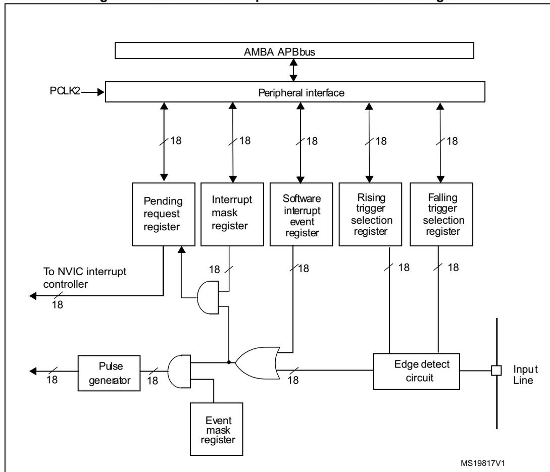
The block diagram illustrates the internal architecture of the External interrupt/event controller (EXTI). At the top, the AMBA APBbus is connected to a Peripheral interface . The PCLK2 clock signal is also input to this interface. Below the interface, five 18-bit wide registers are shown: Pending request register , Interrupt mask register , Software interrupt event register , Rising trigger selection register , and Falling trigger selection register . These registers are connected to the Peripheral interface and to various logic blocks. The Pending request register outputs to the To NVIC interrupt controller . The Interrupt mask register and Software interrupt event register are inputs to an AND gate. The output of this AND gate is connected to an OR gate. The Rising trigger selection register and Falling trigger selection register are inputs to an Edge detect circuit , which receives signals from Input Line s. The output of the Edge detect circuit is also connected to the OR gate. The Event mask register is an input to the OR gate. The output of the OR gate is connected to a second AND gate. The Pulse generator is an input to this second AND gate. The output of the second AND gate is connected to the To NVIC interrupt controller . Bus widths are indicated by a slash and the number 18 on the signal lines.
8.2.3 Wakeup event management
The STM32F100xx is able to handle external or internal events in order to wake up the core (WFE). The wakeup event can be generated either by:
- • enabling an interrupt in the peripheral control register but not in the NVIC, and enabling the SEVONPEND bit in the Cortex®-M3 System Control register. When the MCU resumes from WFE, the peripheral interrupt pending bit and the peripheral NVIC IRQ channel pending bit (in the NVIC interrupt clear pending register) have to be cleared.
- • or configuring an external or internal EXTI line in event mode. When the CPU resumes from WFE, it is not necessary to clear the peripheral interrupt pending bit or the NVIC IRQ channel pending bit as the pending bit corresponding to the event line is not set.
To use an external line as a wakeup event, refer to Section 8.2.4: Functional description .
8.2.4 Functional description
To generate the interrupt, the interrupt line should be configured and enabled. This is done by programming the two trigger registers with the desired edge detection and by enabling the interrupt request by writing a '1' to the corresponding bit in the interrupt mask register. When the selected edge occurs on the external interrupt line, an interrupt request is generated. The pending bit corresponding to the interrupt line is also set. This request is reset by writing a '1' in the pending register.
To generate the event, the event line should be configured and enabled. This is done by programming the two trigger registers with the desired edge detection and by enabling the event request by writing a '1' to the corresponding bit in the event mask register. When the selected edge occurs on the event line, an event pulse is generated. The pending bit corresponding to the event line is not set
An interrupt/event request can also be generated by software by writing a '1' in the software interrupt/event register.
Hardware interrupt selection
To configure the 18 lines as interrupt sources, use the following procedure:
- • Configure the mask bits of the 18 Interrupt lines (EXTI_IMR)
- • Configure the Trigger Selection bits of the Interrupt lines (EXTI_RTSR and EXTI_FTSR)
- • Configure the enable and mask bits that control the NVIC IRQ channel mapped to the External Interrupt Controller (EXTI) so that an interrupt coming from one of the 18 lines can be correctly acknowledged.
Hardware event selection
To configure the 18 lines as event sources, use the following procedure:
- • Configure the mask bits of the 18 Event lines (EXTI_EMR)
- • Configure the Trigger Selection bits of the Event lines (EXTI_RTSR and EXTI_FTSR)
Software interrupt/event selection
The 18 lines can be configured as software interrupt/event lines. The following is the procedure to generate a software interrupt.
- • Configure the mask bits of the 18 Interrupt/Event lines (EXTI_IMR, EXTI_EMR)
- • Set the required bit of the software interrupt register (EXTI_SWIER)
8.2.5 External interrupt/event line mapping
The 112 GPIOs are connected to the 16 external interrupt/event lines in the following manner:
Figure 19. External interrupt/event GPIO mapping
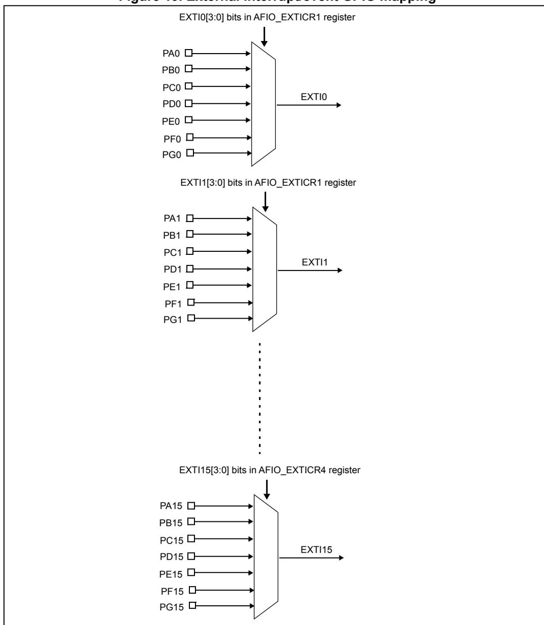
The diagram illustrates the mapping of external interrupt/event lines to GPIO pins. It consists of three multiplexer blocks, each controlled by a specific register bit field:
- EXTI0:
Controlled by the
EXTI0[3:0]bits in theAFIO_EXTICR1register. The multiplexer selects betweenPA0,PB0,PC0,PD0,PE0,PF0, andPG0. - EXTI1:
Controlled by the
EXTI1[3:0]bits in theAFIO_EXTICR1register. The multiplexer selects betweenPA1,PB1,PC1,PD1,PE1,PF1, andPG1. - EXTI15:
Controlled by the
EXTI15[3:0]bits in theAFIO_EXTICR4register. The multiplexer selects betweenPA15,PB15,PC15,PD15,PE15,PF15, andPG15.
A vertical dashed line between the
EXTI1
and
EXTI15
blocks indicates that the same mapping logic applies to the intermediate interrupt lines (EXTI2 through EXTI14).
- 1. To configure the
AFIO_EXTICRxfor the mapping of external interrupt/event lines onto GPIOs, theAFIOclock should first be enabled. Refer to Section 6.3.7: APB2 peripheral clock enable register (RCC_APB2ENR) .
The two other EXTI lines are connected as follows:
- • EXTI line 16 is connected to the PVD output
- • EXTI line 17 is connected to the RTC Alarm event
8.3 EXTI registers
Refer to
Section 1.1 on page 32
for a list of abbreviations used in register descriptions.
The peripheral registers have to be accessed by words (32-bit).
8.3.1 Interrupt mask register (EXTI_IMR)
Address offset: 0x00
Reset value: 0x0000 0000
| 31 | 30 | 29 | 28 | 27 | 26 | 25 | 24 | 23 | 22 | 21 | 20 | 19 | 18 | 17 | 16 |
|---|---|---|---|---|---|---|---|---|---|---|---|---|---|---|---|
| Reserved | MR17 | MR16 | |||||||||||||
| rw | rw | ||||||||||||||
| 15 | 14 | 13 | 12 | 11 | 10 | 9 | 8 | 7 | 6 | 5 | 4 | 3 | 2 | 1 | 0 |
| MR15 | MR14 | MR13 | MR12 | MR11 | MR10 | MR9 | MR8 | MR7 | MR6 | MR5 | MR4 | MR3 | MR2 | MR1 | MR0 |
| rw | rw | rw | rw | rw | rw | rw | rw | rw | rw | rw | rw | rw | rw | rw | rw |
Bits 31:18 Reserved, must be kept at reset value (0).
Bits 17:0
MRx
: Interrupt Mask on line x
0: Interrupt request from Line x is masked
1: Interrupt request from Line x is not masked
8.3.2 Event mask register (EXTI_EMR)
Address offset: 0x04
Reset value: 0x0000 0000
| 31 | 30 | 29 | 28 | 27 | 26 | 25 | 24 | 23 | 22 | 21 | 20 | 19 | 18 | 17 | 16 |
|---|---|---|---|---|---|---|---|---|---|---|---|---|---|---|---|
| Reserved | MR17 | MR16 | |||||||||||||
| rw | rw | ||||||||||||||
| 15 | 14 | 13 | 12 | 11 | 10 | 9 | 8 | 7 | 6 | 5 | 4 | 3 | 2 | 1 | 0 |
| MR15 | MR14 | MR13 | MR12 | MR11 | MR10 | MR9 | MR8 | MR7 | MR6 | MR5 | MR4 | MR3 | MR2 | MR1 | MR0 |
| rw | rw | rw | rw | rw | rw | rw | rw | rw | rw | rw | rw | rw | rw | rw | rw |
Bits 31:18 Reserved, must be kept at reset value (0).
Bits 17:0
MRx
: Event mask on line x
0: Event request from Line x is masked
1: Event request from Line x is not masked
8.3.3 Rising trigger selection register (EXTI_RTSR)
Address offset: 0x08
Reset value: 0x0000 0000
| 31 | 30 | 29 | 28 | 27 | 26 | 25 | 24 | 23 | 22 | 21 | 20 | 19 | 18 | 17 | 16 |
|---|---|---|---|---|---|---|---|---|---|---|---|---|---|---|---|
| Reserved | TR17 | TR16 | |||||||||||||
| rw | rw | ||||||||||||||
| 15 | 14 | 13 | 12 | 11 | 10 | 9 | 8 | 7 | 6 | 5 | 4 | 3 | 2 | 1 | 0 |
| TR15 | TR14 | TR13 | TR12 | TR11 | TR10 | TR9 | TR8 | TR7 | TR6 | TR5 | TR4 | TR3 | TR2 | TR1 | TR0 |
| rw | rw | rw | rw | rw | rw | rw | rw | rw | rw | rw | rw | rw | rw | rw | rw |
Bits 31:18 Reserved, must be kept at reset value (0).
Bits 17:0 TRx : Rising trigger event configuration bit of line x
0: Rising trigger disabled (for Event and Interrupt) for input line
1: Rising trigger enabled (for Event and Interrupt) for input line
Note: The external wakeup lines are edge triggered, no glitches must be generated on these lines. If a rising edge on external interrupt line occurs during writing of EXTI_RTSR register, the pending bit will not be set.
Rising and Falling edge triggers can be set for the same interrupt line. In this configuration, both generate a trigger condition.
8.3.4 Falling trigger selection register (EXTI_FTSR)
Address offset: 0x0C
Reset value: 0x0000 0000
| 31 | 30 | 29 | 28 | 27 | 26 | 25 | 24 | 23 | 22 | 21 | 20 | 19 | 18 | 17 | 16 |
|---|---|---|---|---|---|---|---|---|---|---|---|---|---|---|---|
| Reserved | TR17 | TR16 | |||||||||||||
| rw | rw | ||||||||||||||
| 15 | 14 | 13 | 12 | 11 | 10 | 9 | 8 | 7 | 6 | 5 | 4 | 3 | 2 | 1 | 0 |
| TR15 | TR14 | TR13 | TR12 | TR11 | TR10 | TR9 | TR8 | TR7 | TR6 | TR5 | TR4 | TR3 | TR2 | TR1 | TR0 |
| rw | rw | rw | rw | rw | rw | rw | rw | rw | rw | rw | rw | rw | rw | rw | rw |
Bits 31:18 Reserved, must be kept at reset value (0).
Bits 17:0 TRx : Falling trigger event configuration bit of line x
0: Falling trigger disabled (for Event and Interrupt) for input line
1: Falling trigger enabled (for Event and Interrupt) for input line
Note: The external wakeup lines are edge triggered, no glitches must be generated on these lines. If a falling edge on external interrupt line occurs during writing of EXTI_FTSR register, the pending bit will not be set.
Rising and Falling edge triggers can be set for the same interrupt line. In this configuration, both generate a trigger condition.
8.3.5 Software interrupt event register (EXTI_SWIER)
Address offset: 0x10
Reset value: 0x0000 0000
| 31 | 30 | 29 | 28 | 27 | 26 | 25 | 24 | 23 | 22 | 21 | 20 | 19 | 18 | 17 | 16 |
|---|---|---|---|---|---|---|---|---|---|---|---|---|---|---|---|
| Reserved | SWIER 17 | SWIER 16 | |||||||||||||
| rw | rw | ||||||||||||||
| 15 | 14 | 13 | 12 | 11 | 10 | 9 | 8 | 7 | 6 | 5 | 4 | 3 | 2 | 1 | 0 |
| SWIER 15 | SWIER 14 | SWIER 13 | SWIER 12 | SWIER 11 | SWIER 10 | SWIER 9 | SWIER 8 | SWIER 7 | SWIER 6 | SWIER 5 | SWIER 4 | SWIER 3 | SWIER 2 | SWIER 1 | SWIER 0 |
| rw | rw | rw | rw | rw | rw | rw | rw | rw | rw | rw | rw | rw | rw | rw | rw |
Bits 31:18 Reserved, must be kept at reset value (0).
Bits 17:0 SWIERx : Software interrupt on line x
If the interrupt is enabled on this line in the EXTI_IMR, writing a '1' to this bit when it is at '0' sets the corresponding pending bit in EXTI_PR resulting in an interrupt request generation. This bit is cleared by clearing the corresponding bit of EXTI_PR (by writing a 1 into the bit)
8.3.6 Pending register (EXTI_PR)
Address offset: 0x14
Reset value: undefined
| 31 | 30 | 29 | 28 | 27 | 26 | 25 | 24 | 23 | 22 | 21 | 20 | 19 | 18 | 17 | 16 |
|---|---|---|---|---|---|---|---|---|---|---|---|---|---|---|---|
| Reserved | PR17 | PR16 | |||||||||||||
| rc_w1 | rc_w1 | ||||||||||||||
| 15 | 14 | 13 | 12 | 11 | 10 | 9 | 8 | 7 | 6 | 5 | 4 | 3 | 2 | 1 | 0 |
| PR15 | PR14 | PR13 | PR12 | PR11 | PR10 | PR9 | PR8 | PR7 | PR6 | PR5 | PR4 | PR3 | PR2 | PR1 | PR0 |
| rc_w1 | rc_w1 | rc_w1 | rc_w1 | rc_w1 | rc_w1 | rc_w1 | rc_w1 | rc_w1 | rc_w1 | rc_w1 | rc_w1 | rc_w1 | rc_w1 | rc_w1 | rc_w1 |
Bits 31:18 Reserved, must be kept at reset value (0).
Bits 17:0 PRx : Pending bit
0: No trigger request occurred
1: selected trigger request occurred
This bit is set when the selected edge event arrives on the external interrupt line. This bit is cleared by writing a '1' into the bit.
8.3.7 EXTI register map
The following table gives the EXTI register map and the reset values.
Table 51. External interrupt/event controller register map and reset values
| Offset | Register | 31 | 30 | 29 | 28 | 27 | 26 | 25 | 24 | 23 | 22 | 21 | 20 | 19 | 18 | 17 | 16 | 15 | 14 | 13 | 12 | 11 | 10 | 9 | 8 | 7 | 6 | 5 | 4 | 3 | 2 | 1 | 0 |
|---|---|---|---|---|---|---|---|---|---|---|---|---|---|---|---|---|---|---|---|---|---|---|---|---|---|---|---|---|---|---|---|---|---|
| 0x00 | EXTI_IMR | Reserved | MR[17:0] | ||||||||||||||||||||||||||||||
| Reset value | 0 | 0 | 0 | 0 | 0 | 0 | 0 | 0 | 0 | 0 | 0 | 0 | 0 | 0 | 0 | 0 | 0 | 0 | 0 | 0 | 0 | 0 | 0 | 0 | 0 | 0 | 0 | 0 | 0 | 0 | 0 | 0 | |
| 0x04 | EXTI_EMR | Reserved | EMR[17:0] | ||||||||||||||||||||||||||||||
| Reset value | 0 | 0 | 0 | 0 | 0 | 0 | 0 | 0 | 0 | 0 | 0 | 0 | 0 | 0 | 0 | 0 | 0 | 0 | 0 | 0 | 0 | 0 | 0 | 0 | 0 | 0 | 0 | 0 | 0 | 0 | 0 | 0 | |
| 0x08 | EXTI_RTSR | Reserved | RTSR[17:0] | ||||||||||||||||||||||||||||||
| Reset value | 0 | 0 | 0 | 0 | 0 | 0 | 0 | 0 | 0 | 0 | 0 | 0 | 0 | 0 | 0 | 0 | 0 | 0 | 0 | 0 | 0 | 0 | 0 | 0 | 0 | 0 | 0 | 0 | 0 | 0 | 0 | 0 | |
| 0x0C | EXTI_FTSR | Reserved | FTSR[17:0] | ||||||||||||||||||||||||||||||
| Reset value | 0 | 0 | 0 | 0 | 0 | 0 | 0 | 0 | 0 | 0 | 0 | 0 | 0 | 0 | 0 | 0 | 0 | 0 | 0 | 0 | 0 | 0 | 0 | 0 | 0 | 0 | 0 | 0 | 0 | 0 | 0 | 0 | |
| 0x10 | EXTI_SWIER | Reserved | SWIER[17:0] | ||||||||||||||||||||||||||||||
| Reset value | 0 | 0 | 0 | 0 | 0 | 0 | 0 | 0 | 0 | 0 | 0 | 0 | 0 | 0 | 0 | 0 | 0 | 0 | 0 | 0 | 0 | 0 | 0 | 0 | 0 | 0 | 0 | 0 | 0 | 0 | 0 | 0 | |
| 0x14 | EXTI_PR | Reserved | PR[17:0] | ||||||||||||||||||||||||||||||
| Reset value | 0 | 0 | 0 | 0 | 0 | 0 | 0 | 0 | 0 | 0 | 0 | 0 | 0 | 0 | 0 | 0 | 0 | 0 | 0 | 0 | 0 | 0 | 0 | 0 | 0 | 0 | 0 | 0 | 0 | 0 | 0 | 0 | |
Refer to Table 1 on page 37 and Table 2 on page 38 for the register boundary addresses.