7. General-purpose and alternate-function I/Os (GPIOs and AFIOs)
Low-density value line devices are STM32F100xx microcontrollers where the flash memory density ranges between 16 and 32 Kbytes.
Medium-density value line devices are STM32F100xx microcontrollers where the flash memory density ranges between 64 and 128 Kbytes.
High-density value line devices are STM32F100xx microcontrollers where the flash memory density ranges between 256 and 512 Kbytes.
This section applies to the whole STM32F100xx family, unless otherwise specified.
7.1 GPIO functional description
Each of the general-purpose I/O ports has two 32-bit configuration registers (GPIOx_CRL, GPIOx_CRH), two 32-bit data registers (GPIOx_IDR, GPIOx_ODR), a 32-bit set/reset register (GPIOx_BSRR), a 16-bit reset register (GPIOx_BRR) and a 32-bit locking register (GPIOx_LCKR).
Subject to the specific hardware characteristics of each I/O port listed in the datasheet , each port bit of the General Purpose IO (GPIO) Ports, can be individually configured by software in several modes:
- • Input floating
- • Input pull-up
- • Input pull-down
- • Analog
- • Output open-drain
- • Output push-pull
- • Alternate function push-pull
- • Alternate function open-drain
Each I/O port bit is freely programmable, however the I/O port registers have to be accessed as 32-bit words (half-word or byte accesses are not allowed). The purpose of the GPIOx_BSRR and GPIOx_BRR registers is to allow atomic read/modify accesses to any of the GPIO registers. This way, there is no risk that an IRQ occurs between the read and the modify access.
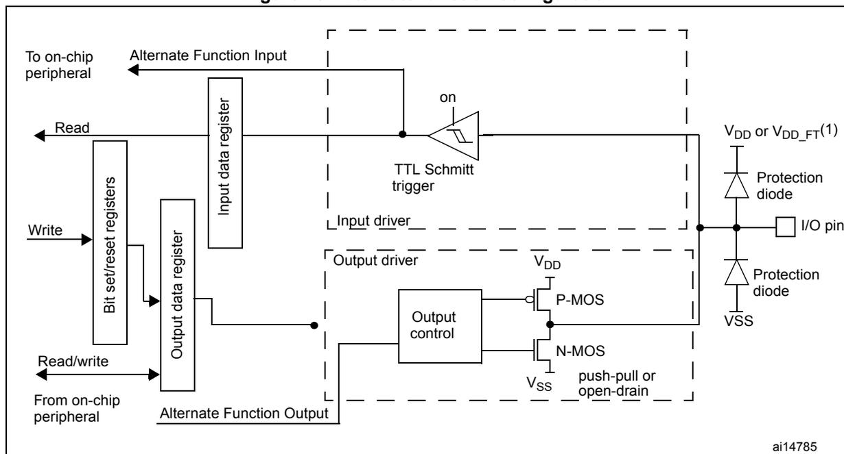
Figure 11 shows the basic structure of an I/O Port bit.
Figure 11. Basic structure of a standard I/O port bit
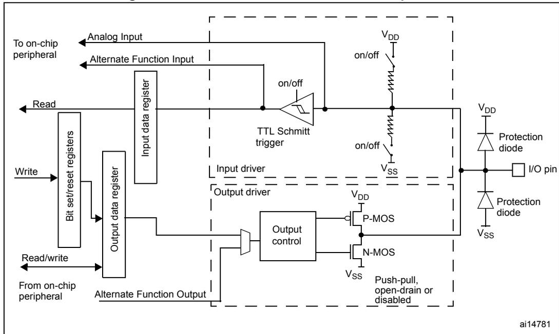
This schematic diagram illustrates the internal architecture of a standard I/O port bit. On the left, external signals enter the chip: 'Analog Input' and 'Alternate Function Input' connect to an 'Input driver' containing a 'TTL Schmitt trigger'. The 'Input driver' is connected to an 'Input data register', which is read by 'Read' signals from on-chip peripherals. Below this, 'Bit set/reset registers' are used to 'Write' to the 'Output data register'. The 'Output data register' is controlled by 'Read/write' signals from on-chip peripherals and provides 'Alternate Function Output'. The 'Output data register' connects to an 'Output control' block, which drives a pair of 'P-MOS' and 'N-MOS' transistors configured as a 'Push-pull, open-drain or disabled' output driver. The 'Output driver' is connected to an 'I/O pin' through 'Protection diode' structures. Pull-up and pull-down resistors are connected between the internal signal lines and \( V_{DD} \) and \( V_{SS} \) respectively, with 'on/off' switches. The identifier 'ai14781' is located in the bottom right corner.
Figure 12. Basic structure of a 5-Volt tolerant I/O port bit
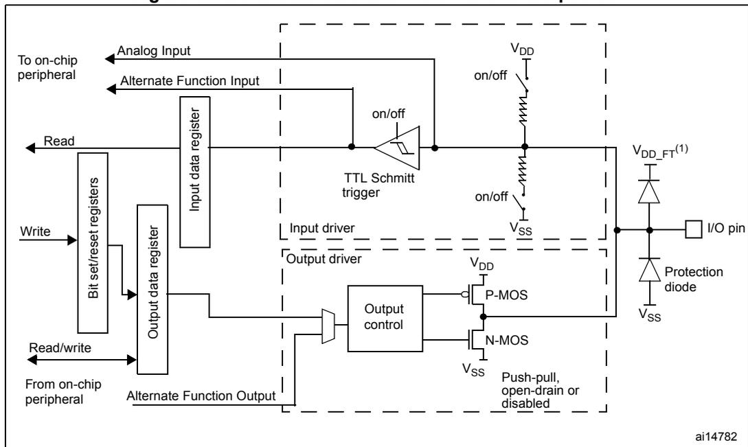
This schematic diagram shows the internal architecture of a 5-Volt tolerant I/O port bit. It shares the same input and output driver stages as Figure 11, including 'Analog Input', 'Alternate Function Input', 'Input driver' with 'TTL Schmitt trigger', 'Input data register', 'Bit set/reset registers', 'Output data register', 'Output control', and 'P-MOS/N-MOS' drivers. The key difference is in the protection circuitry at the 'I/O pin'. Instead of a standard diode to \( V_{DD} \) , it features a protection structure involving \( V_{DD\_FT}^{(1)} \) and a 'Protection diode' to \( V_{SS} \) . Pull-up and pull-down resistors to \( V_{DD} \) and \( V_{SS} \) are also present. The identifier 'ai14782' is located in the bottom right corner.
1. \( V_{DD\_FT} \) is a potential specific to 5-Volt tolerant I/Os, and different from \( V_{DD} \) .
Table 16. Port bit configuration table
| Configuration mode | CNF1 | CNF0 | MODE1 | MODE0 | PxODR register | |
|---|---|---|---|---|---|---|
| General purpose output | Push-pull | 0 | 0 | 01 | 0 or 1 | |
| Open-drain | 1 | 0 or 1 | ||||
| Alternate Function output | Push-pull | 1 | 0 | 11 | see Table 17 | Don't care |
| Open-drain | 1 | Don't care | ||||
| Input | Analog | 0 | 0 | 00 | Don't care | |
| Input floating | 1 | Don't care | ||||
| Input pull-down | 1 | 0 | 0 | |||
| Input pull-up | 1 | |||||
Table 17. Output MODE bits
| MODE[1:0] | Meaning |
|---|---|
| 00 | Reserved |
| 01 | Maximum output speed 10 MHz |
| 10 | Maximum output speed 2 MHz |
| 11 | Maximum output speed 50 MHz |
7.1.1 General-purpose I/O (GPIO)
During and just after reset, the alternate functions are not active and the I/O ports are configured in Input Floating mode (CNFx[1:0]=01b, MODEx[1:0]=00b).
The JTAG pins are in input PU/PD after reset:
PA15: JTDI in PU
PA14: JTCK in PD
PA13: JTMS in PU
PB4: NJTRST in PU
When configured as output, the value written to the Output Data register (GPIOx_ODR) is output on the I/O pin. It is possible to use the output driver in Push-Pull mode or Open-Drain mode (only the N-MOS is activated when outputting 0).
The Input Data register (GPIOx_IDR) captures the data present on the I/O pin at every APB2 clock cycle.
All GPIO pins have an internal weak pull-up and weak pull-down that can be activated or not when configured as input.
7.1.2 Atomic bit set or reset
There is no need for the software to disable interrupts when programming the GPIOx_ODR at bit level: it is possible to modify only one or several bits in a single atomic APB2 write access. This is achieved by programming to '1' the Bit Set/Reset register (GPIOx_BSRR, or
for reset only GPIOx_BRR) to select the bits to modify. The unselected bits will not be modified.
7.1.3 External interrupt/wakeup lines
All ports have external interrupt capability. To use external interrupt lines, the port must be configured in input mode. For more information on external interrupts, refer to Section 8.2: External interrupt/event controller (EXTI) and Section 8.2.3: Wakeup event management .
7.1.4 Alternate functions (AF)
It is necessary to program the Port Bit Configuration register before using a default alternate function.
- • For alternate function inputs, the port must be configured in Input mode (floating, pull-up or pull-down) and the input pin must be driven externally.
Note: It is also possible to emulate the AF input pin by software by programming the GPIO controller. In this case, the port should be configured in Alternate Function Output mode. And obviously, the corresponding port should not be driven externally as it will be driven by the software using the GPIO controller.
- • For alternate function outputs, the port must be configured in Alternate Function Output mode (Push-Pull or Open-Drain).
- • For bidirectional Alternate Functions, the port bit must be configured in Alternate Function Output mode (Push-Pull or Open-Drain). In this case the input driver is configured in input floating mode
If a port bit is configured as Alternate Function Output, this disconnects the output register and connects the pin to the output signal of an on-chip peripheral.
If software configures a GPIO pin as Alternate Function Output, but peripheral is not activated, its output is not specified.
7.1.5 Software remapping of I/O alternate functions
To optimize the number of peripheral I/O functions for different device packages, it is possible to remap some alternate functions to some other pins. This is achieved by software, by programming the corresponding registers (refer to AFIO registers ). In that case, the alternate functions are no longer mapped to their original assignations.
7.1.6 GPIO locking mechanism
The locking mechanism allows the IO configuration to be frozen. When the LOCK sequence has been applied on a port bit, it is no longer possible to modify the value of the port bit until the next reset.
7.1.7 Input configuration
When the I/O Port is programmed as Input:
- • The Output Buffer is disabled
- • The Schmitt Trigger Input is activated
- • The weak pull-up and pull-down resistors are activated or not depending on input configuration (pull-up, pull-down or floating):
- • The data present on the I/O pin is sampled into the Input Data register every APB2 clock cycle
- • A read access to the Input Data register obtains the I/O State.
Figure 13 shows the Input Configuration of the I/O Port bit.
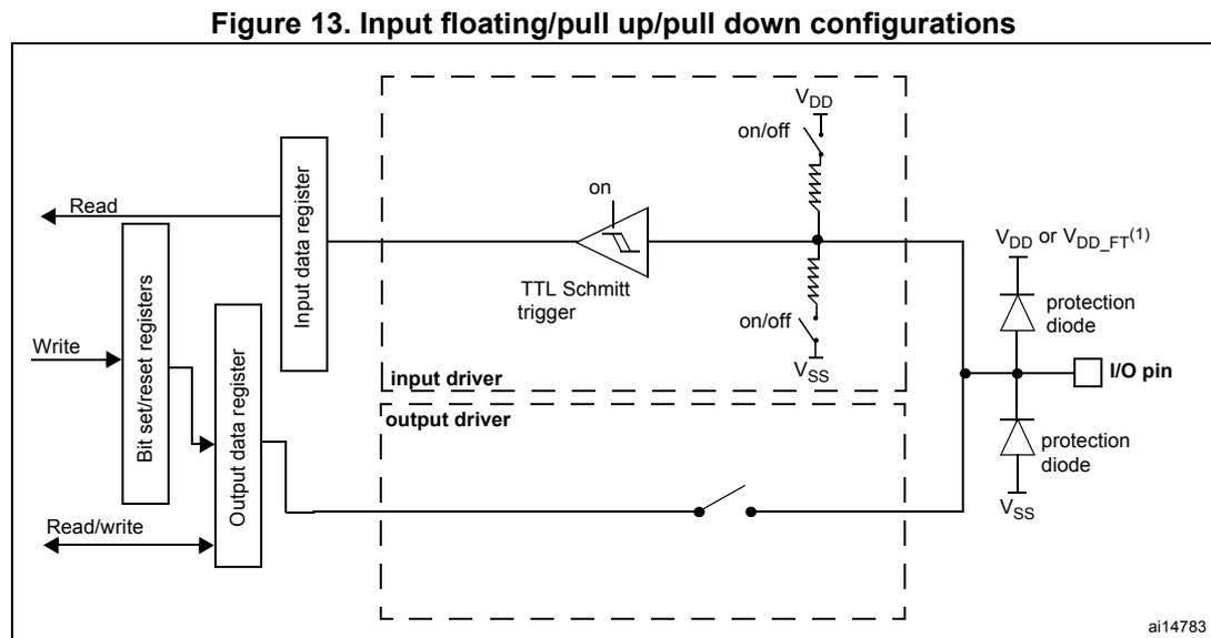
Figure 13. Input floating/pull up/pull down configurations
1. \( V_{DD\_FT} \) is a potential specific to 5-Volt tolerant I/Os, and different from \( V_{DD} \) .
7.1.8 Output configuration
When the I/O Port is programmed as Output:
- • The Output Buffer is enabled:
- – Open Drain mode: A “0” in the Output register activates the N-MOS while a “1” in the Output register leaves the port in Hi-Z (the P-MOS is never activated)
- – Push-Pull mode: A “0” in the Output register activates the N-MOS while a “1” in the Output register activates the P-MOS
- • The Schmitt Trigger Input is activated.
- • The weak pull-up and pull-down resistors are disabled.
- • The data present on the I/O pin is sampled into the Input Data register every APB2 clock cycle
- • A read access to the Input Data register gets the I/O state in open drain mode
- • A read access to the Output Data register gets the last written value in Push-Pull mode
Figure 14 shows the Output configuration of the I/O Port bit.
Figure 14. Output configuration
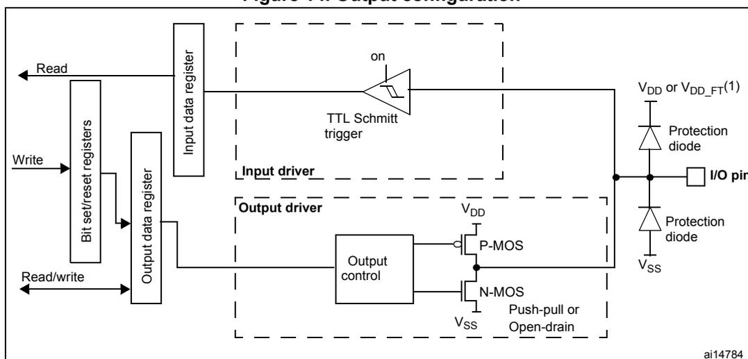
1. \( V_{DD\_FT} \) is a potential specific to 5-Volt tolerant I/Os, and different from \( V_{DD} \) .
7.1.9 Alternate function configuration
When the I/O Port is programmed as Alternate Function:
- • The Output Buffer is turned on in Open Drain or Push-Pull configuration
- • The Output Buffer is driven by the signal coming from the peripheral (alternate function out)
- • The Schmitt Trigger Input is activated
- • The weak pull-up and pull-down resistors are disabled.
- • The data present on the I/O pin is sampled into the Input Data register every APB2 clock cycle
- • A read access to the Input Data register gets the I/O state in open drain mode
- • A read access to the Output Data register gets the last written value in Push-Pull mode
Figure 15 shows the Alternate Function Configuration of the I/O Port bit. Also, refer to Section 7.4: AFIO registers for further information.
A set of Alternate Function I/O registers allows the user to remap some alternate functions to different pins. Refer to Section 7.3: Alternate function I/O and debug configuration (AFIO) .
Figure 15. Alternate function configuration
1. \( V_{DD\_FT} \) is a potential specific to 5-Volt tolerant I/Os, and different from \( V_{DD} \) .
7.1.10 Analog configuration
When the I/O Port is programmed as Analog configuration:
- • The Output Buffer is disabled.
- • The Schmitt Trigger Input is de-activated providing zero consumption for every analog value of the I/O pin. The output of the Schmitt Trigger is forced to a constant value (0).
- • The weak pull-up and pull-down resistors are disabled.
- • Read access to the Input Data register gets the value “0”.
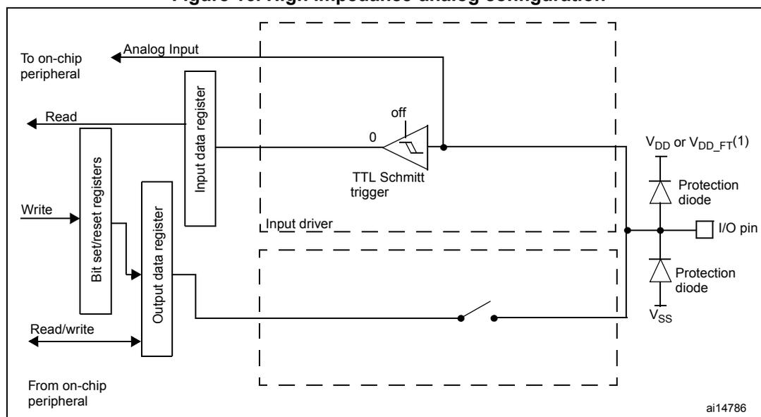
Figure 16 shows the high impedance-analog configuration of the I/O Port bit.
Figure 16. High impedance-analog configuration
7.1.11 GPIO configurations for device peripherals
Table 18 to Table 27 give the GPIO configurations of the device peripherals.
Table 18. Advanced timer TIM1
| TIM1 pinout | Configuration | GPIO configuration |
|---|---|---|
| TIM1_CHx | Input capture channel x | Input floating |
| Output compare channel x | Alternate function push-pull | |
| TIM1_CHxN | Complementary output channel x | Alternate function push-pull |
| TIM1_BKIN | Break input | Input floating |
| TIM1_ETR | External trigger timer input | Input floating |
Table 19. General-purpose timers TIM2/3/4/5
| TIM2/3/4/5 pinout | Configuration | GPIO configuration |
|---|---|---|
| TIM2/3/4/5_CHx | Input capture channel x | Input floating |
| Output compare channel x | Alternate function push-pull | |
| TIM2/3/4/5_ETR | External trigger timer input | Input floating |
Table 20. General-purpose timers TIM15/16/17
| TIM15/16/17 pinout | Configuration | GPIO configuration |
|---|---|---|
| TIM15/16/17_CHx | Input capture channel x | Input floating |
| Output compare channel x | Alternate function push-pull | |
| TIM15/16/17_CHxN | Complementary output channel x | Alternate function push-pull |
| TIM15/16/17 pinout | Configuration | GPIO configuration |
|---|---|---|
| TIM15/16/17_BKIN | Break input | Input floating |
| TIM15/16/17_ETR | External trigger timer input | Input floating |
| TIM12/13/14 pinout | Configuration | GPIO configuration |
|---|---|---|
| TIM12/13/14_CHx | Input capture channel x | Input floating |
| Output compare channel x | Alternate function push-pull |
| USART pinout | Configuration | GPIO configuration |
|---|---|---|
| USARTx_TX (1) | Full duplex | Alternate function push-pull |
| Half duplex synchronous mode | Alternate function push-pull | |
| USARTx_RX | Full duplex | Input floating / Input pull-up |
| Half duplex synchronous mode | Not used. Can be used as a general IO | |
| USARTx_CK | Synchronous mode | Alternate function push-pull |
| USARTx_RTS | Hardware flow control | Alternate function push-pull |
| USARTx_CTS | Hardware flow control | Input floating/ Input pull-up |
1. The USART_TX pin can also be configured as alternate function open drain.
Table 23. SPI| SPI pinout | Configuration | GPIO configuration |
|---|---|---|
| SPIx_SCK | Master | Alternate function push-pull |
| Slave | Input floating | |
| SPIx_MOSI | Full duplex / master | Alternate function push-pull |
| Full duplex / slave | Input floating / Input pull-up | |
| Simplex bidirectional data wire / master | Alternate function push-pull | |
| Simplex bidirectional data wire/ slave | Not used. Can be used as a GPIO | |
| SPIx_MISO | Full duplex / master | Input floating / Input pull-up |
| Full duplex / slave (point to point) | Alternate function push-pull | |
| Full duplex / slave (multi-slave) | Alternate function open drain | |
| Simplex bidirectional data wire / master | Not used. Can be used as a GPIO | |
| Simplex bidirectional data wire/ slave (point to point) | Alternate function push-pull | |
| Simplex bidirectional data wire/ slave (multi-slave) | Alternate function open drain |
Table 23. SPI (continued)
| SPI pinout | Configuration | GPIO configuration |
|---|---|---|
| SPIx_NSS | Hardware master /slave | Input floating/ Input pull-up / Input pull-down |
| Hardware master/ NSS output enabled | Alternate function push-pull | |
| Software | Not used. Can be used as a GPIO |
Table 24. CEC
| CEC pinout | Configuration | GPIO configuration |
|---|---|---|
| CEC | CEC line | Alternate function open drain |
Table 25. I2C
| I2C pinout | Configuration | GPIO configuration |
|---|---|---|
| I2Cx_SCL | I2C clock | Alternate function open drain |
| I2Cx_SDA | I2C Data I/O | Alternate function open drain |
The GPIO configuration of the ADC inputs should be analog.
Figure 17. ADC / DAC
| ADC/DAC pin | GPIO configuration |
|---|---|
| ADC/DAC | Analog |
Table 26. FSMC
| FSMC pinout | GPIO configuration |
|---|---|
| FSMC_A[25:0] FSMC_D[15:0] | Alternate function push-pull |
| FSMC_CK | Alternate function push-pull |
| FSMC_NOE FSMC_NWE | Alternate function push-pull |
| FSMC_NE[4:1] | Alternate function push-pull |
| FSMC_NWAIT | Input floating/ Input pull-up |
| FSMC_NL FSMC_NBL[1:0] | Alternate function push-pull |
Table 27. Other I/Os
| Pins | Alternate function | GPIO configuration |
|---|---|---|
| TAMPER-RTC pin | RTC output | Forced by hardware when configuring the BKP_CR and BKP_RTCCR registers |
| Tamper event input | ||
| MCO | Clock output | Alternate function push-pull |
| EXTI input lines | External input interrupts | Input floating / input pull-up / input pull-down |
7.2 GPIO registers
Refer to Section 1.1 on page 32 for a list of abbreviations used in register descriptions.
The peripheral registers have to be accessed by words (32-bit).
7.2.1 Port configuration register low (GPIOx_CRL) (x=A..G)
Address offset: 0x00
Reset value: 0x4444 4444
| 31 | 30 | 29 | 28 | 27 | 26 | 25 | 24 | 23 | 22 | 21 | 20 | 19 | 18 | 17 | 16 |
|---|---|---|---|---|---|---|---|---|---|---|---|---|---|---|---|
| CNF7[1:0] | MODE7[1:0] | CNF6[1:0] | MODE6[1:0] | CNF5[1:0] | MODE5[1:0] | CNF4[1:0] | MODE4[1:0] | ||||||||
| rw | rw | rw | rw | rw | rw | rw | rw | rw | rw | rw | rw | rw | rw | rw | rw |
| 15 | 14 | 13 | 12 | 11 | 10 | 9 | 8 | 7 | 6 | 5 | 4 | 3 | 2 | 1 | 0 |
| CNF3[1:0] | MODE3[1:0] | CNF2[1:0] | MODE2[1:0] | CNF1[1:0] | MODE1[1:0] | CNF0[1:0] | MODE0[1:0] | ||||||||
| rw | rw | rw | rw | rw | rw | rw | rw | rw | rw | rw | rw | rw | rw | rw | rw |
Bits 31:30, 27:26, 23:22, 19:18, 15:14, 11:10, 7:6, 3:2
CNFy[1:0]
: Port x configuration bits (y= 0 .. 7)
These bits are written by software to configure the corresponding I/O port.
Refer to
Table 16: Port bit configuration table
.
In input mode (MODE[1:0]=00):
- 00: Analog mode
- 01: Floating input (reset state)
- 10: Input with pull-up / pull-down
- 11: Reserved
In output mode (MODE[1:0] > 00):
- 00: General purpose output push-pull
- 01: General purpose output Open-drain
- 10: Alternate function output Push-pull
- 11: Alternate function output Open-drain
Bits 29:28, 25:24, 21:20, 17:16, 13:12, 9:8, 5:4, 1:0
MODEy[1:0]
: Port x mode bits (y= 0 .. 7)
These bits are written by software to configure the corresponding I/O port.
Refer to
Table 16: Port bit configuration table
.
- 00: Input mode (reset state)
- 01: Output mode, max speed 10 MHz.
- 10: Output mode, max speed 2 MHz.
- 11: Output mode, max speed 50 MHz.
7.2.2 Port configuration register high (GPIOx_CRH) (x=A..G)
Address offset: 0x04
Reset value: 0x4444 4444
| 31 | 30 | 29 | 28 | 27 | 26 | 25 | 24 | 23 | 22 | 21 | 20 | 19 | 18 | 17 | 16 |
|---|---|---|---|---|---|---|---|---|---|---|---|---|---|---|---|
| CNF15[1:0] | MODE15[1:0] | CNF14[1:0] | MODE14[1:0] | CNF13[1:0] | MODE13[1:0] | CNF12[1:0] | MODE12[1:0] | ||||||||
| rw | rw | rw | rw | rw | rw | rw | rw | rw | rw | rw | rw | rw | rw | rw | rw |
| 15 | 14 | 13 | 12 | 11 | 10 | 9 | 8 | 7 | 6 | 5 | 4 | 3 | 2 | 1 | 0 |
| CNF11[1:0] | MODE11[1:0] | CNF10[1:0] | MODE10[1:0] | CNF9[1:0] | MODE9[1:0] | CNF8[1:0] | MODE8[1:0] | ||||||||
| rw | rw | rw | rw | rw | rw | rw | rw | rw | rw | rw | rw | rw | rw | rw | rw |
Bits 31:30, 27:26,
CNFy[1:0]
: Port x configuration bits (y= 8 .. 15)
23:22, 19:18, 15:14, 11:10, 7:6, 3:2 These bits are written by software to configure the corresponding I/O port.
Refer to
Table 16: Port bit configuration table
.
In input mode (MODE[1:0]=00):
- 00: Analog mode
- 01: Floating input (reset state)
- 10: Input with pull-up / pull-down
- 11: Reserved
In output mode (MODE[1:0] > 00):
- 00: General purpose output push-pull
- 01: General purpose output Open-drain
- 10: Alternate function output Push-pull
- 11: Alternate function output Open-drain
Bits 29:28, 25:24,
MODEy[1:0]
: Port x mode bits (y= 8 .. 15)
21:20, 17:16, 13:12, 9:8, 5:4, 1:0 These bits are written by software to configure the corresponding I/O port.
Refer to
Table 16: Port bit configuration table
.
- 00: Input mode (reset state)
- 01: Output mode, max speed 10 MHz.
- 10: Output mode, max speed 2 MHz.
- 11: Output mode, max speed 50 MHz.
7.2.3 Port input data register (GPIOx_IDR) (x=A..G)
Address offset: 0x08h
Reset value: 0x0000 XXXX
| 31 | 30 | 29 | 28 | 27 | 26 | 25 | 24 | 23 | 22 | 21 | 20 | 19 | 18 | 17 | 16 |
|---|---|---|---|---|---|---|---|---|---|---|---|---|---|---|---|
| Reserved | |||||||||||||||
| 15 | 14 | 13 | 12 | 11 | 10 | 9 | 8 | 7 | 6 | 5 | 4 | 3 | 2 | 1 | 0 |
| IDR15 | IDR14 | IDR13 | IDR12 | IDR11 | IDR10 | IDR9 | IDR8 | IDR7 | IDR6 | IDR5 | IDR4 | IDR3 | IDR2 | IDR1 | IDR0 |
| r | r | r | r | r | r | r | r | r | r | r | r | r | r | r | r |
Bits 31:16 Reserved, must be kept at reset value.
Bits 15:0 IDRy : Port input data (y= 0 .. 15)
These bits are read only and can be accessed in Word mode only. They contain the input value of the corresponding I/O port.
7.2.4 Port output data register (GPIOx_ODR) (x=A..G)
Address offset: 0x0C
Reset value: 0x0000 0000
| 31 | 30 | 29 | 28 | 27 | 26 | 25 | 24 | 23 | 22 | 21 | 20 | 19 | 18 | 17 | 16 |
|---|---|---|---|---|---|---|---|---|---|---|---|---|---|---|---|
| Reserved | |||||||||||||||
| 15 | 14 | 13 | 12 | 11 | 10 | 9 | 8 | 7 | 6 | 5 | 4 | 3 | 2 | 1 | 0 |
| ODR15 | ODR14 | ODR13 | ODR12 | ODR11 | ODR10 | ODR9 | ODR8 | ODR7 | ODR6 | ODR5 | ODR4 | ODR3 | ODR2 | ODR1 | ODR0 |
| rw | rw | rw | rw | rw | rw | rw | rw | rw | rw | rw | rw | rw | rw | rw | rw |
Bits 31:16 Reserved, must be kept at reset value.
Bits 15:0 ODRy : Port output data (y= 0 .. 15)
These bits can be read and written by software and can be accessed in Word mode only.
Note: For atomic bit set/reset, the ODR bits can be individually set and cleared by writing to the GPIOx_BSRR register (x = A .. E).
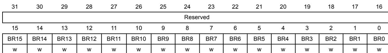
7.2.5 Port bit set/reset register (GPIOx_BSRR) (x=A..G)
Address offset: 0x10
Reset value: 0x0000 0000
| 31 | 30 | 29 | 28 | 27 | 26 | 25 | 24 | 23 | 22 | 21 | 20 | 19 | 18 | 17 | 16 |
|---|---|---|---|---|---|---|---|---|---|---|---|---|---|---|---|
| BR15 | BR14 | BR13 | BR12 | BR11 | BR10 | BR9 | BR8 | BR7 | BR6 | BR5 | BR4 | BR3 | BR2 | BR1 | BR0 |
| w | w | w | w | w | w | w | w | w | w | w | w | w | w | w | w |
| 15 | 14 | 13 | 12 | 11 | 10 | 9 | 8 | 7 | 6 | 5 | 4 | 3 | 2 | 1 | 0 |
| BS15 | BS14 | BS13 | BS12 | BS11 | BS10 | BS9 | BS8 | BS7 | BS6 | BS5 | BS4 | BS3 | BS2 | BS1 | BS0 |
| w | w | w | w | w | w | w | w | w | w | w | w | w | w | w | w |
Bits 31:16 BRy : Port x Reset bit y (y= 0 .. 15)
These bits are write-only and can be accessed in Word mode only.
0: No action on the corresponding ODRx bit
1: Reset the corresponding ODRx bit
Note: If both BSx and BRx are set, BSx has priority.
Bits 15:0 BSy : Port x Set bit y (y= 0 .. 15)
These bits are write-only and can be accessed in Word mode only.
0: No action on the corresponding ODRx bit
1: Set the corresponding ODRx bit
7.2.6 Port bit reset register (GPIOx_BRR) (x=A..G)
Address offset: 0x14
Reset value: 0x0000 0000
| 31 | 30 | 29 | 28 | 27 | 26 | 25 | 24 | 23 | 22 | 21 | 20 | 19 | 18 | 17 | 16 |
| Reserved | |||||||||||||||
| 15 | 14 | 13 | 12 | 11 | 10 | 9 | 8 | 7 | 6 | 5 | 4 | 3 | 2 | 1 | 0 |
| BR15 | BR14 | BR13 | BR12 | BR11 | BR10 | BR9 | BR8 | BR7 | BR6 | BR5 | BR4 | BR3 | BR2 | BR1 | BR0 |
| w | w | w | w | w | w | w | w | w | w | w | w | w | w | w | w |
Bits 31:16 Reserved
Bits 15:0 BRy : Port x Reset bit y (y= 0 .. 15)
These bits are write-only and can be accessed in Word mode only.
0: No action on the corresponding ODRx bit
1: Reset the corresponding ODRx bit
7.2.7 Port configuration lock register (GPIOx_LCKR) (x=A..G)
This register is used to lock the configuration of the port bits when a correct write sequence is applied to bit 16 (LCKK). The value of bits [15:0] is used to lock the configuration of the GPIO. During the write sequence, the value of LCKR[15:0] must not change. When the LOCK sequence has been applied on a port bit it is no longer possible to modify the value of the port bit until the next reset.
Each lock bit freezes the corresponding 4 bits of the control register (CRL, CRH).
Address offset: 0x18
Reset value: 0x0000 0000
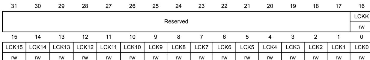
| 31 | 30 | 29 | 28 | 27 | 26 | 25 | 24 | 23 | 22 | 21 | 20 | 19 | 18 | 17 | 16 |
| Reserved | LCKK | ||||||||||||||
| rw | |||||||||||||||
| 15 | 14 | 13 | 12 | 11 | 10 | 9 | 8 | 7 | 6 | 5 | 4 | 3 | 2 | 1 | 0 |
| LCK15 | LCK14 | LCK13 | LCK12 | LCK11 | LCK10 | LCK9 | LCK8 | LCK7 | LCK6 | LCK5 | LCK4 | LCK3 | LCK2 | LCK1 | LCK0 |
| rw | rw | rw | rw | rw | rw | rw | rw | rw | rw | rw | rw | rw | rw | rw | rw |
Bits 31:17 Reserved
Bit 16 LCKK[16] : Lock key
This bit can be read anytime. It can only be modified using the Lock Key Writing Sequence.
0: Port configuration lock key not active
1: Port configuration lock key active. GPIOx_LCKR register is locked until the next reset.
LOCK key writing sequence:
Write 1
Write 0
Write 1
Read 0
Read 1 (this read is optional but confirms that the lock is active)
Note: During the LOCK Key Writing sequence, the value of LCK[15:0] must not change.
Any error in the lock sequence will abort the lock.
Bits 15:0 LCKy : Port x Lock bit y (y= 0 .. 15)
These bits are read write but can only be written when the LCKK bit is 0.
0: Port configuration not locked
1: Port configuration locked.
7.3 Alternate function I/O and debug configuration (AFIO)
To optimize the number of peripherals available for the 64-pin or the 100-pin or the 144-pin package, it is possible to remap some alternate functions to some other pins. This is achieved by software, by programming the AF remap and debug I/O configuration register (AFIO_MAPR) . In this case, the alternate functions are no longer mapped to their original assignments.
7.3.1 Using OSC32_IN/OSC32_OUT pins as GPIO ports PC14/PC15
The LSE oscillator pins OSC32_IN and OSC32_OUT can be used as general-purpose I/O PC14 and PC15, respectively, when the LSE oscillator is off. The LSE has priority over the GP IOs function.
Note: The PC14/PC15 GPIO functionality is lost when the 1.8 V domain is powered off (by entering standby mode) or when the backup domain is supplied by V BAT (V DD no more supplied). In this case the IOs are set in analog mode.
Refer to the note on IO usage restrictions in Section 4.1.2: Battery backup domain .
7.3.2 Using OSC_IN/OSC_OUT pins as GPIO ports PD0/PD1
The HSE oscillator pins OSC_IN/OSC_OUT can be used as general-purpose I/O PD0/PD1 by programming the PD01_REMAP bit in the AF remap and debug I/O configuration register (AFIO_MAPR) .
This remap is available only on 48- and 64-pin packages (PD0 and PD1 are available on 100-pin and 144-pin packages, no need for remapping).
Note: The external interrupt/event function is not remapped. PD0 and PD1 cannot be used for external interrupt/event generation on 48- and 64-pin packages.
7.3.3 JTAG/SWD alternate function remapping
The debug interface signals are mapped on the GPIO ports as shown in Table 28 .
Table 28. Debug interface signals
| Alternate function | GPIO port |
|---|---|
| JTMS / SWDIO | PA13 |
| JTCK / SWCLK | PA14 |
| JTDI | PA15 |
| JTDO / TRACESWO | PB3 |
| NJTRST | PB4 |
| TRACECK | PE2 |
| TRACED0 | PE3 |
| TRACED1 | PE4 |
| TRACED2 | PE5 |
| TRACED3 | PE6 |
To optimize the number of free GPIOs during debugging, this mapping can be configured in different ways by programming the SWJ_CFG[1:0] bits in the AF remap and debug I/O configuration register (AFIO_MAPR) . Refer to Table 29 .
Table 29. Debug port mapping
| SWJ_CFG [2:0] | Available debug ports | SWJ I/O pin assigned | ||||
|---|---|---|---|---|---|---|
| PA13 / JTMS/ SWDIO | PA14 / JTCK/S WCLK | PA15 / JTDI | PB3 / JTDO/ TRACE SWO | PB4/ NJTRST | ||
| 000 | Full SWJ (JTAG-DP + SW-DP) (Reset state) | X | X | X | X | X |
| 001 | Full SWJ (JTAG-DP + SW-DP) but without NJTRST | X | X | X | x | Free |
| 010 | JTAG-DP Disabled and SW-DP Enabled | X | X | Free | Free (1) | Free |
| 100 | JTAG-DP Disabled and SW-DP Disabled | Free | Free | Free | Free | Free |
| Other | Forbidden | - | - | - | - | - |
1. Released only if not using asynchronous trace.
7.3.4 Timer alternate function remapping
Timer 4 channels 1 to 4 can be remapped from Port B to Port D. Other timer remapping possibilities are listed in Table 35 to Table 37 . Refer to AF remap and debug I/O configuration register (AFIO_MAPR) .
Table 30. TIM5 alternate function remapping (1)| Alternate function | TIM5CH4_IREMAP = 0 | TIM5CH4_IREMAP = 1 |
|---|---|---|
| TIM5_CH4 | TIM5 Channel 4 is connected to PA3 | LSI internal clock is connected to TIM5_CH4 input for calibration purpose. |
- 1. Remap available only for high-density value line devices.
| Alternate function | TIM12_REMAP = 0 | TIM12_REMAP = 1 |
|---|---|---|
| TIM12_CH1 | PC4 | PB12 |
| TIM12_CH2 | PC5 | PB13 |
- 1. Refer to the AF remap and debug I/O configuration register Section 7.4.7: AF remap and debug I/O configuration register (AFIO_MAPR2) . Remap available only for high-density value line devices.
| Alternate function | TIM13_REMAP = 0 | TIM13_REMAP = 1 |
|---|---|---|
| TIM13_CH1 | PC8 | PB0 |
- 1. Refer to the AF remap and debug I/O configuration register Section 7.4.7: AF remap and debug I/O configuration register (AFIO_MAPR2) . Remap available only for high-density value line devices.
| Alternate function | TIM14_REMAP = 0 | TIM14_REMAP = 1 |
|---|---|---|
| TIM14_CH1 | PC9 | PB1 |
- 1. Refer to the AF remap and debug I/O configuration register Section 7.4.7: AF remap and debug I/O configuration register (AFIO_MAPR2) . Remap available only for high-density value line devices.
| Alternate function | TIM4_REMAP = 0 | TIM4_REMAP = 1 (1) |
|---|---|---|
| TIM4_CH1 | PB6 | PD12 |
| TIM4_CH2 | PB7 | PD13 |
| TIM4_CH3 | PB8 | PD14 |
| TIM4_CH4 | PB9 | PD15 |
- 1. Remap available only for 100-pin and for 144-pin package.
| Alternate function | TIM3_REMAP[1:0] = "00" (no remap) | TIM3_REMAP[1:0] = "10" (partial remap) | TIM3_REMAP[1:0] = "11" (full remap) (1) |
|---|---|---|---|
| TIM3_CH1 | PA6 | PB4 | PC6 |
| TIM3_CH2 | PA7 | PB5 | PC7 |
| TIM3_CH3 | PB0 | PC8 | |
| TIM3_CH4 | PB1 | PC9 |
- 1. Remap available only for 64-pin, 100-pin and 144-pin packages.
| Alternate function | TIM2_REMAP [1:0] = "00" (no remap) | TIM2_REMAP [1:0] = "01" (partial remap) | TIM2_REMAP [1:0] = "10" (partial remap) | TIM2_REMAP [1:0] = "11" (full remap) |
|---|---|---|---|---|
| TIM2_CH1_ETR (1) | PA0 | PA15 | PA0 | PA15 |
| TIM2_CH2 | PA1 | PB3 | PA1 | PB3 |
| TIM2_CH3 | PA2 | PB10 | ||
| TIM2_CH4 | PA3 | PB11 | ||
- 1. TIM_CH1 and TIM_ETR share the same pin but cannot be used at the same time (which is why we have this notation: TIM2_CH1_ETR).
| Alternate functions mapping | TIM1_REMAP[1:0] = "00" (no remap) | TIM1_REMAP[1:0] = "01" (partial remap) | TIM1_REMAP[1:0] = "11" (full remap) (1) |
|---|---|---|---|
| TIM1_ETR | PA12 | PE7 | |
| TIM1_CH1 | PA8 | PE9 | |
| TIM1_CH2 | PA9 | PE11 | |
| TIM1_CH3 | PA10 | PE13 | |
| TIM1_CH4 | PA11 | PE14 | |
| TIM1_BKIN | PB12 | PA6 | PE15 |
| TIM1_CH1N | PB13 | PA7 | PE8 |
| TIM1_CH2N | PB14 (2) | PB0 | PE10 |
| TIM1_CH3N | PB15 (2) | PB1 | PE12 |
- 1. Remap available only for 100-pin and 144-pin packages.
| DMA requests | TIM1_DMA_REMAP = 0 | TIM1_DMA_REMAP = 1 |
|---|---|---|
| TIM1_CH1 DMA request | Mapped on DMA1 Channel2 | Mapped on DMA1 Channel6 |
| TIM1_CH2 DMA request | Mapped on DMA1 Channel3 | Mapped on DMA1 Channel6 |
- 1. Refer to the AF remap and debug I/O configuration register Section 7.4.7: AF remap and debug I/O configuration register (AFIO_MAPR2) .
| Alternate function | TIM15_REMAP = 0 | TIM15_REMAP = 1 |
|---|---|---|
| TIM15_CH1 | PA2 | PB14 |
| TIM15_CH2 | PA3 | PB15 |
- 1. Refer to the AF remap and debug I/O configuration register Section 7.4.7: AF remap and debug I/O configuration register (AFIO_MAPR2) .
| Alternate function | TIM16_REMAP = 0 | TIM16_REMAP = 1 |
|---|---|---|
| TIM16_CH1 | PB8 | PA6 |
- 1. Refer to the AF remap and debug I/O configuration register Section 7.4.7: AF remap and debug I/O configuration register (AFIO_MAPR2) .
| Alternate function | TIM17_REMAP = 0 | TIM17_REMAP = 1 |
|---|---|---|
| TIM17_CH1 | PB9 | PA7 |
- 1. Refer to the AF remap and debug I/O configuration register Section 7.4.7: AF remap and debug I/O configuration register (AFIO_MAPR2) .
7.3.5 USART alternate function remapping
Refer to AF remap and debug I/O configuration register (AFIO_MAPR) .
Table 42. USART3 remapping
| Alternate function | USART3_REMAP[1:0] = "00" (no remap) | USART3_REMAP[1:0] = "01" (partial remap) (1) | USART3_REMAP[1:0] = "11" (full remap) (2) |
|---|---|---|---|
| USART3_TX | PB10 | PC10 | PD8 |
| USART3_RX | PB11 | PC11 | PD9 |
| USART3_CK | PB12 | PC12 | PD10 |
| USART3_CTS | PB13 | PD11 | |
| USART3_RTS | PB14 | PD12 | |
- 1. Remap available only for 64-pin, 100-pin and 144-pin packages
- 2. Remap available only for 100-pin and 144-pin packages.
Table 43. USART2 remapping
| Alternate functions | USART2_REMAP = 0 | USART2_REMAP = 1 (1) |
|---|---|---|
| USART2_CTS | PA0 | PD3 |
| USART2_RTS | PA1 | PD4 |
| USART2_TX | PA2 | PD5 |
| USART2_RX | PA3 | PD6 |
| USART2_CK | PA4 | PD7 |
- 1. Remap available only for 100-pin and 144-pin packages.
Table 44. USART1 remapping
| Alternate function | USART1_REMAP = 0 | USART1_REMAP = 1 |
|---|---|---|
| USART1_TX | PA9 | PB6 |
| USART1_RX | PA10 | PB7 |
7.3.6 I2C1 alternate function remapping
Refer to AF remap and debug I/O configuration register (AFIO_MAPR)
Table 45. I2C1 remapping
| Alternate function | I2C1_REMAP = 0 | I2C1_REMAP = 1 |
|---|---|---|
| I2C1_SCL | PB6 | PB8 |
| I2C1_SDA | PB7 | PB9 |
7.3.7 SPI1 alternate function remapping
Refer to AF remap and debug I/O configuration register (AFIO_MAPR)
Table 46. SPI1 remapping
| Alternate function | SPI1_REMAP = 0 | SPI1_REMAP = 1 |
|---|---|---|
| SPI1_NSS | PA4 | PA15 |
| SPI1_SCK | PA5 | PB3 |
| SPI1_MISO | PA6 | PB4 |
| SPI1_MOSI | PA7 | PB5 |
7.3.8 CEC remap
Refer to Section 7.4.7: AF remap and debug I/O configuration register (AFIO_MAPR2) .
Table 47. CEC remapping
| Alternate function | CEC_REMAP = 0 | CEC_REMAP = 1 |
|---|---|---|
| CEC | PB8 | PB10 |
7.4 AFIO registers
Refer to Section 1.1 on page 32 for a list of abbreviations used in register descriptions.
Note: To read/write the AFIO_EVCR, AFIO_MAPR, AFIO_MAPR2 and AFIO_EXTICRX registers, the AFIO clock should first be enabled. Refer to APB2 peripheral clock enable register (RCC_APB2ENR) .
The peripheral registers have to be accessed by words (32-bit).
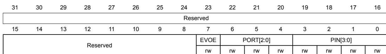
7.4.1 Event control register (AFIO_EVCR)
Address offset: 0x00
Reset value: 0x0000 0000
| 31 | 30 | 29 | 28 | 27 | 26 | 25 | 24 | 23 | 22 | 21 | 20 | 19 | 18 | 17 | 16 |
| Reserved | |||||||||||||||
| 15 | 14 | 13 | 12 | 11 | 10 | 9 | 8 | 7 | 6 | 5 | 4 | 3 | 2 | 1 | 0 |
| Reserved | EVOE | PORT[2:0] | PIN[3:0] | ||||||||||||
| rw | rw | rw | rw | rw | rw | rw | rw | ||||||||
Bits 31:8 Reserved
Bit 7 EVOE : Event output enable
Set and cleared by software. When set the EVENTOUT Cortex ® output is connected to the I/O selected by the PORT[2:0] and PIN[3:0] bits.
Bits 3:0 PIN[3:0] : Pin selection (x = A .. E)
Set and cleared by software. Select the pin used to output the Cortex ® EVENTOUT signal.
0000: Px0 selected
0001: Px1 selected
0010: Px2 selected
0011: Px3 selected
...
1111: Px15 selected
7.4.2 AF remap and debug I/O configuration register (AFIO_MAPR)
Address offset: 0x04
Reset value: 0x0000 0000
| 31 | 30 | 29 | 28 | 27 | 26 | 25 | 24 | 23 | 22 | 21 | 20 | 19 | 18 | 17 | 16 |
|---|---|---|---|---|---|---|---|---|---|---|---|---|---|---|---|
| Reserved | SWJ_CFG[2:0] | Reserved | TIM5CH4_IREMAP | ||||||||||||
| w | w | w | rw | ||||||||||||
| 15 | 14 | 13 | 12 | 11 | 10 | 9 | 8 | 7 | 6 | 5 | 4 | 3 | 2 | 1 | 0 |
| PD01_REMAP | Reserved | TIM4_REMAP | TIM3_REMAP [1:0] | TIM2_REMAP [1:0] | TIM1_REMAP [1:0] | USART3_REMAP[1:0] | USART2_REMAP | USART1_REMAP | I2C1_REMAP | SPI1_REMAP | |||||
| rw | rw | rw | rw | rw | rw | rw | rw | rw | rw | rw | rw | rw | rw | ||
Bits 31:27 Reserved
Bits 26:24 SWJ_CFG[2:0] : Serial wire JTAG configuration
These bits are write-only (when read, the value is undefined). They are used to configure the SWJ and trace alternate function I/Os. The SWJ (Serial Wire JTAG) supports JTAG or SWD access to the Cortex® debug port. The default state after reset is SWJ ON without trace. This allows JTAG or SW mode to be enabled by sending a specific sequence on the JTMS / JTCCK pin.
000: Full SWJ (JTAG-DP + SW-DP): Reset State
001: Full SWJ (JTAG-DP + SW-DP) but without NJTRST
010: JTAG-DP Disabled and SW-DP Enabled
100: JTAG-DP Disabled and SW-DP Disabled
Other combinations: no effect
Bits 23:17 Reserved.
Bit 15 PD01_REMAP : Port D0/Port D1 mapping on OSC_IN/OSC_OUT
This bit is set and cleared by software. It controls the mapping of PD0 and PD1 GPIO functionality. When the HSE oscillator is not used (application running on internal 8 MHz RC) PD0 and PD1 can be mapped on OSC_IN and OSC_OUT. This is available only on 48- and 64-pin packages (PD0 and PD1 are available on 100-pin packages, no need for remapping).
0: No remapping of PD0 and PD1
1: PD0 remapped on OSC_IN, PD1 remapped on OSC_OUT,
Bits 14:13 Reserved.
Bit 12 TIM4_REMAP : TIM4 remapping
This bit is set and cleared by software. It controls the mapping of TIM4 channels 1 to 4 onto the GPIO ports.
0: No remap (TIM4_CH1/PB6, TIM4_CH2/PB7, TIM4_CH3/PB8, TIM4_CH4/PB9)
1: Full remap (TIM4_CH1/PD12, TIM4_CH2/PD13, TIM4_CH3/PD14, TIM4_CH4/PD15)
Note: TIM4_ETR on PE0 is not re-mapped.
Bits 11:10 TIM3_REMAP[1:0] : TIM3 remapping
These bits are set and cleared by software. They control the mapping of TIM3 channels 1 to 4 on the GPIO ports.
00: No remap (CH1/PA6, CH2/PA7, CH3/PB0, CH4/PB1)
01: Not used
10: Partial remap (CH1/PB4, CH2/PB5, CH3/PB0, CH4/PB1)
11: Full remap (CH1/PC6, CH2/PC7, CH3/PC8, CH4/PC9)
Note: TIM3_ETR on PE0 is not re-mapped.
Bits 9:8 TIM2_REMAP[1:0]: TIM2 remappingThese bits are set and cleared by software. They control the mapping of TIM2 channels 1 to 4 and external trigger (ETR) on the GPIO ports.
00: No remap (CH1/ETR/PA0, CH2/PA1, CH3/PA2, CH4/PA3)
01: Partial remap (CH1/ETR/PA15, CH2/PB3, CH3/PA2, CH4/PA3)
10: Partial remap (CH1/ETR/PA0, CH2/PA1, CH3/PB10, CH4/PB11)
11: Full remap (CH1/ETR/PA15, CH2/PB3, CH3/PB10, CH4/PB11)
Bits 7:6 TIM1_REMAP[1:0]: TIM1 remappingThese bits are set and cleared by software. They control the mapping of TIM1 channels 1 to 4, 1N to 3N, external trigger (ETR) and Break input (BKIN) on the GPIO ports.
00: No remap (ETR/PA12, CH1/PA8, CH2/PA9, CH3/PA10, CH4/PA11, BKIN/PB12, CH1N/PB13, CH2N/PB14, CH3N/PB15)
01: Partial remap (ETR/PA12, CH1/PA8, CH2/PA9, CH3/PA10, CH4/PA11, BKIN/PA6, CH1N/PA7, CH2N/PB0, CH3N/PB1)
10: not used
11: Full remap (ETR/PE7, CH1/PE9, CH2/PE11, CH3/PE13, CH4/PE14, BKIN/PE15, CH1N/PE8, CH2N/PE10, CH3N/PE12)
Bits 5:4 USART3_REMAP[1:0]: USART3 remappingThese bits are set and cleared by software. They control the mapping of USART3 CTS, RTS, CK, TX and RX alternate functions on the GPIO ports.
00: No remap (TX/PB10, RX/PB11, CK/PB12, CTS/PB13, RTS/PB14)
01: Partial remap (TX/PC10, RX/PC11, CK/PC12, CTS/PB13, RTS/PB14)
10: not used
11: Full remap (TX/PD8, RX/PD9, CK/PD10, CTS/PD11, RTS/PD12)
Bit 3 USART2_REMAP: USART2 remappingThis bit is set and cleared by software. It controls the mapping of USART2 CTS, RTS, CK, TX and RX alternate functions on the GPIO ports.
0: No remap (CTS/PA0, RTS/PA1, TX/PA2, RX/PA3, CK/PA4)
1: Remap (CTS/PD3, RTS/PD4, TX/PD5, RX/PD6, CK/PD7)
Bit 2 USART1_REMAP: USART1 remappingThis bit is set and cleared by software. It controls the mapping of USART1 TX and RX alternate functions on the GPIO ports.
0: No remap (TX/PA9, RX/PA10)
1: Remap (TX/PB6, RX/PB7)
Bit 1 I2C1_REMAP: I2C1 remappingThis bit is set and cleared by software. It controls the mapping of I2C1 SCL and SDA alternate functions on the GPIO ports.
0: No remap (SCL/PB6, SDA/PB7)
1: Remap (SCL/PB8, SDA/PB9)
Bit 0 SPI1_REMAP: SPI1 remappingThis bit is set and cleared by software. It controls the mapping of SPI1 NSS, SCK, MISO, MOSI alternate functions on the GPIO ports.
0: No remap (NSS/PA4, SCK/PA5, MISO/PA6, MOSI/PA7)
1: Remap (NSS/PA15, SCK/PB3, MISO/PB4, MOSI/PB5)
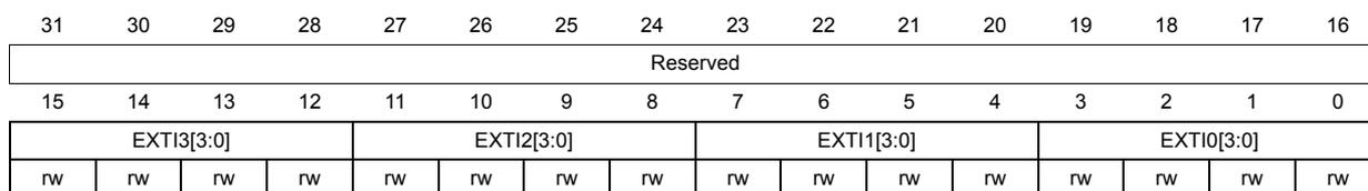
7.4.3 External interrupt configuration register 1 (AFIO_EXTICR1)
Address offset: 0x08
Reset value: 0x0000
| 31 | 30 | 29 | 28 | 27 | 26 | 25 | 24 | 23 | 22 | 21 | 20 | 19 | 18 | 17 | 16 |
| Reserved | |||||||||||||||
| 15 | 14 | 13 | 12 | 11 | 10 | 9 | 8 | 7 | 6 | 5 | 4 | 3 | 2 | 1 | 0 |
| EXTI3[3:0] | EXTI2[3:0] | EXTI1[3:0] | EXTI0[3:0] | ||||||||||||
| rw | rw | rw | rw | rw | rw | rw | rw | rw | rw | rw | rw | rw | rw | rw | rw |
Bits 31:16 Reserved
Bits 15:0 EXTIx[3:0] : EXTI x configuration (x= 0 to 3)
These bits are written by software to select the source input for EXTIx external interrupt.
Refer to Section 8.2.5: External interrupt/event line mapping
0000: PA[x] pin
0001: PB[x] pin
0010: PC[x] pin
0011: PD[x] pin
0100: PE[x] pin
0101: PF[x] pin
0110: PG[x] pin
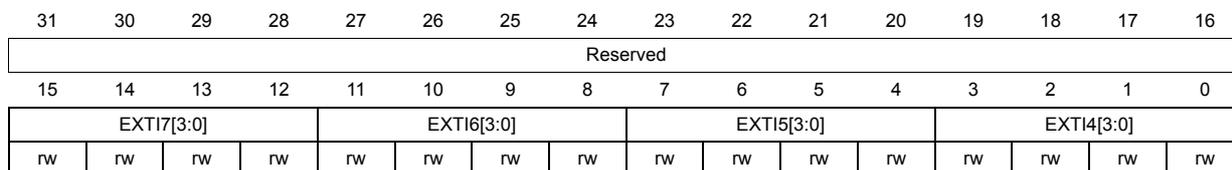
7.4.4 External interrupt configuration register 2 (AFIO_EXTICR2)
Address offset: 0x0C
Reset value: 0x0000
| 31 | 30 | 29 | 28 | 27 | 26 | 25 | 24 | 23 | 22 | 21 | 20 | 19 | 18 | 17 | 16 |
| Reserved | |||||||||||||||
| 15 | 14 | 13 | 12 | 11 | 10 | 9 | 8 | 7 | 6 | 5 | 4 | 3 | 2 | 1 | 0 |
| EXTI7[3:0] | EXTI6[3:0] | EXTI5[3:0] | EXTI4[3:0] | ||||||||||||
| rw | rw | rw | rw | rw | rw | rw | rw | rw | rw | rw | rw | rw | rw | rw | rw |
Bits 31:16 Reserved
Bits 15:0 EXTIx[3:0] : EXTI x configuration (x= 4 to 7)
These bits are written by software to select the source input for EXTIx external interrupt.
0000: PA[x] pin
0001: PB[x] pin
0010: PC[x] pin
0011: PD[x] pin
0100: PE[x] pin
0101: PF[x] pin
0110: PG[x] pin
7.4.5 External interrupt configuration register 3 (AFIO_EXTICR3)
Address offset: 0x10
Reset value: 0x0000

| 31 | 30 | 29 | 28 | 27 | 26 | 25 | 24 | 23 | 22 | 21 | 20 | 19 | 18 | 17 | 16 |
| Reserved | |||||||||||||||
| 15 | 14 | 13 | 12 | 11 | 10 | 9 | 8 | 7 | 6 | 5 | 4 | 3 | 2 | 1 | 0 |
| EXTI11[3:0] | EXTI10[3:0] | EXTI9[3:0] | EXTI8[3:0] | ||||||||||||
| rw | rw | rw | rw | rw | rw | rw | rw | rw | rw | rw | rw | rw | rw | rw | rw |
Bits 31:16 Reserved
Bits 15:0 EXTIx[3:0] : EXTI x configuration (x= 8 to 11)
These bits are written by software to select the source input for EXTIx external interrupt.
- 0000: PA[x] pin
- 0001: PB[x] pin
- 0010: PC[x] pin
- 0011: PD[x] pin
- 0100: PE[x] pin
- 0101: PF[x] pin
- 0110: PG[x] pin
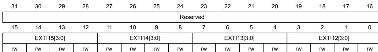
7.4.6 External interrupt configuration register 4 (AFIO_EXTICR4)
Address offset: 0x14
Reset value: 0x0000
| 31 | 30 | 29 | 28 | 27 | 26 | 25 | 24 | 23 | 22 | 21 | 20 | 19 | 18 | 17 | 16 |
| Reserved | |||||||||||||||
| 15 | 14 | 13 | 12 | 11 | 10 | 9 | 8 | 7 | 6 | 5 | 4 | 3 | 2 | 1 | 0 |
| EXTI15[3:0] | EXTI14[3:0] | EXTI13[3:0] | EXTI12[3:0] | ||||||||||||
| rw | rw | rw | rw | rw | rw | rw | rw | rw | rw | rw | rw | rw | rw | rw | rw |
Bits 31:16 Reserved
Bits 15:0 EXTIx[3:0] : EXTI x configuration (x= 12 to 15)
These bits are written by software to select the source input for EXTIx external interrupt.
- 0000: PA[x] pin
- 0001: PB[x] pin
- 0010: PC[x] pin
- 0011: PD[x] pin
- 0100: PE[x] pin
- 0101: PF[x] pin
- 0110: PG[x] pin
7.4.7 AF remap and debug I/O configuration register (AFIO_MAPR2)
Address offset: 0x1C
Reset value: 0x0000 0000
| 31 | 30 | 29 | 28 | 27 | 26 | 25 | 24 | 23 | 22 | 21 | 20 | 19 | 18 | 17 | 16 |
|---|---|---|---|---|---|---|---|---|---|---|---|---|---|---|---|
| Reserved | |||||||||||||||
| 15 | 14 | 13 | 12 | 11 | 10 | 9 | 8 | 7 | 6 | 5 | 4 | 3 | 2 | 1 | 0 |
| Reserved | MISC _REMAP | TIM12_ REMAP | TIM67_ DAC_ DMA_ REMAP | FSMC _NADV | TIM14_ REMAP | TIM13_ REMAP | Reserved | TIM1_ DMA_ REMAP | CEC_ REMAP | TIM17_ REMAP | TIM16_ REMAP | ||||
| rw | rw | rw | rw | rw | rw | rw | rw | rw | rw | ||||||
Bits 31:14 Reserved.
Bit 13 MISC_REMAP : Miscellaneous features remapping.
This bit is set and cleared by software. It controls miscellaneous features
The DMA2 channel 5 interrupt position in the vector table
The timer selection for DAC trigger 3 (TSEL[2:0] = 011, for more details refer to the DAC_CR register).
0: DMA2 channel 5 interrupt is mapped with DMA2 channel 4 at position 59, TIM5 TRGO event is selected as DAC Trigger 3, TIM5 triggers TIM1/3.
1: DMA2 channel 5 interrupt is mapped separately at position 60 and TIM15 TRGO event is selected as DAC Trigger 3, TIM15 triggers TIM1/3.
Note: This bit is available only in high density value line devices.
Bit 12 TIM12_REMAP : TIM12 remapping
This bit is set and cleared by software. It controls the mapping of the TIM12_CH1 and TIM12_CH2 alternate function onto the GPIO ports.
0: No remap (CH1/PC4, CH2/PC5)
1: Remap (CH1/PB12, CH2/PB13)
Note: This bit is available only in high density value line devices.
Bit 11 TIM76_DAC_DMA_REMAP : TIM67_DAC DMA remapping
This bit is set and cleared by software. It controls the mapping of the TIM6_DAC1 and TIM7_DAC2 DMA requests onto the DMA1 channels.
0: No remap (TIM6_DAC1 DMA request/DMA2 Channel3, TIM7_DAC2 DMA request/DMA2 Channel4)
1: Remap (TIM6_DAC1 DMA request/DMA1 Channel3, TIM7_DAC2 DMA request/DMA1 Channel4)
Bit 10 FSMC_NADV : NADV connect/disconnect
This bit is set and cleared by software. It controls the use of the optional FSMC_NADV signal.
0: The NADV signal is connected to the output (default)
1: The NADV signal is not connected. The I/O pin can be used by another peripheral.
Note: This bit is available only in high density value line devices.
Bit 9 TIM14_REMAP : TIM14 remapping
This bit is set and cleared by software. It controls the mapping of the TIM14_CH1 alternate function onto the GPIO ports.
0: No remap (PC9)
1: Remap (PB1)
Bit 8 TIM13_REMAP : TIM13 remappingThis bit is set and cleared by software. It controls the mapping of the TIM13_CH1 alternate function onto the GPIO ports.
0: No remap (PC8)
1: Remap (PB0)
Bits 7:5 Reserved.
Bit 4 TIM1_DMA_REMAP : TIM1 DMA remappingThis bit is set and cleared by software. It controls the mapping of the TIM1 channel 1 and channel 2 DMA requests onto the DMA1 channels.
0: No remap (TIM1_CH1 DMA request/DMA1 Channel2, TIM1_CH2 DMA request/DMA1 Channel3)
1: Remap (TIM1_CH1 DMA request/DMA1 Channel6, TIM1_CH2 DMA request/DMA1 Channel6)
Bit 3 CEC_REMAP : CEC remappingThis bit is set and cleared by software. It controls the mapping of the alternate functions of the CEC line onto the GPIO ports.
0: No remap (CEC/PB8)
1: Remap (CEC/PB10)
Bit 2 TIM17_REMAP : TIM17 remappingThis bit is set and cleared by software. It controls the mapping of the alternate functions of TIM17 channel 1 onto the GPIO ports.
0: No remap (CH1/PB9)
1: Remap (CH1/PA7)
Bit 1 TIM16_REMAP : TIM16 remappingThis bit is set and cleared by software. It controls the mapping of the alternate functions of TIM16 channel 1 onto the GPIO ports.
0: No remap (CH1/PB8)
1: Remap (CH1/PA6)
Bit 0 TIM15_REMAP : TIM15 remappingThis bit is set and cleared by software. It controls the mapping of the alternate functions of TIM15 channels 1 and 2 onto the GPIO ports.
0: No remap (CH1/PA2, CH2/PA3)
1: Remap (CH1/PB14, CH2/PB15)
7.5 GPIO and AFIO register maps
The following tables give the GPIO and AFIO register map and the reset values.
Refer to Table 1 on page 37 and Table 2 on page 38 for the register boundary addresses.
Table 48. GPIO register map and reset values
| Offset | Register | 31 | 30 | 29 | 28 | 27 | 26 | 25 | 24 | 23 | 22 | 21 | 20 | 19 | 18 | 17 | 16 | 15 | 14 | 13 | 12 | 11 | 10 | 9 | 8 | 7 | 6 | 5 | 4 | 3 | 2 | 1 | 0 |
|---|---|---|---|---|---|---|---|---|---|---|---|---|---|---|---|---|---|---|---|---|---|---|---|---|---|---|---|---|---|---|---|---|---|
| 0x00 | GPIOx_CRL | CNF7 [1:0] | MODE7 [1:0] | CNF6 [1:0] | MODE6 [1:0] | CNF5 [1:0] | MODE5 [1:0] | CNF4 [1:0] | MODE4 [1:0] | CNF3 [1:0] | MODE3 [1:0] | CNF2 [1:0] | MODE2 [1:0] | CNF1 [1:0] | MODE1 [1:0] | CNF0 [1:0] | MODE0 [1:0] | ||||||||||||||||
| 0 | 1 | 0 | 0 | 0 | 1 | 0 | 0 | 0 | 1 | 0 | 0 | 0 | 1 | 0 | 0 | 0 | 1 | 0 | 0 | 0 | 1 | 0 | 0 | 0 | 1 | 0 | 0 | 0 | 1 | 0 | 0 | ||
| 0x04 | GPIOx_CRH | CNF15 [1:0] | MODE15 [1:0] | CNF14 [1:0] | MODE14 [1:0] | CNF13 [1:0] | MODE13 [1:0] | CNF12 [1:0] | MODE12 [1:0] | CNF11 [1:0] | MODE11 [1:0] | CNF10 [1:0] | MODE10 [1:0] | CNF9 [1:0] | MODE9 [1:0] | CNF8 [1:0] | MODE8 [1:0] | ||||||||||||||||
| 0 | 1 | 0 | 0 | 0 | 1 | 0 | 0 | 0 | 1 | 0 | 0 | 0 | 1 | 0 | 0 | 0 | 1 | 0 | 0 | 0 | 1 | 0 | 0 | 0 | 1 | 0 | 0 | 0 | 1 | 0 | 0 | ||
| 0x08 | GPIOx_IDR | Reserved | IDRy | ||||||||||||||||||||||||||||||
| 0 | 0 | 0 | 0 | 0 | 0 | 0 | 0 | 0 | 0 | 0 | 0 | 0 | 0 | 0 | 0 | ||||||||||||||||||
| 0x0C | GPIOx_ODR | Reserved | ODRy | ||||||||||||||||||||||||||||||
| 0 | 0 | 0 | 0 | 0 | 0 | 0 | 0 | 0 | 0 | 0 | 0 | 0 | 0 | 0 | 0 | ||||||||||||||||||
| 0x10 | GPIOx_BSRR | BR[15:0] | BSR[15:0] | ||||||||||||||||||||||||||||||
| 0 | 0 | 0 | 0 | 0 | 0 | 0 | 0 | 0 | 0 | 0 | 0 | 0 | 0 | 0 | 0 | 0 | 0 | 0 | 0 | 0 | 0 | 0 | 0 | 0 | 0 | 0 | 0 | 0 | 0 | 0 | 0 | ||
| 0x14 | GPIOx_BRR | Reserved | BR[15:0] | ||||||||||||||||||||||||||||||
| 0 | 0 | 0 | 0 | 0 | 0 | 0 | 0 | 0 | 0 | 0 | 0 | 0 | 0 | 0 | 0 | ||||||||||||||||||
| 0x18 | GPIOx_LCKR | Reserved | LCKK | LCK[15:0] | |||||||||||||||||||||||||||||
| 0 | 0 | 0 | 0 | 0 | 0 | 0 | 0 | 0 | 0 | 0 | 0 | 0 | 0 | 0 | 0 | 0 | |||||||||||||||||
Table 49. AFIO register map and reset values
| Offset | Register | 31 | 30 | 29 | 28 | 27 | 26 | 25 | 24 | 23 | 22 | 21 | 20 | 19 | 18 | 17 | 16 | 15 | 14 | 13 | 12 | 11 | 10 | 9 | 8 | 7 | 6 | 5 | 4 | 3 | 2 | 1 | 0 |
|---|---|---|---|---|---|---|---|---|---|---|---|---|---|---|---|---|---|---|---|---|---|---|---|---|---|---|---|---|---|---|---|---|---|
| 0x00 | AFIO_EVCR | Reserved | EVOE | PORT[2:0] | PIN[3:0] | ||||||||||||||||||||||||||||
| 0 | 0 | 0 | 0 | 0 | 0 | 0 | 0 | ||||||||||||||||||||||||||
| 0x04 | AFIO_MAPR | Reserved | SWJ_CFG[2:0] | Reserved | TIM5CH4_IREMAP | PD01_REMAP | Reserved | TIM4_REMAP | TIM3_REMAP[1:0] | TIM2_REMAP[1:0] | TIM1_REMAP[1:0] | USART3_REMAP[1:0] | USART2_REMAP | USART1_REMAP | I2C1_REMAP | SPI1_REMAP | |||||||||||||||||
| 0 | 0 | 0 | 0 | 0 | 0 | 0 | 0 | 0 | 0 | 0 | 0 | 0 | 0 | 0 | 0 | 0 | 0 | 0 | |||||||||||||||
Table 49. AFIO register map and reset values (continued)
| Offset | Register | 31 | 30 | 29 | 28 | 27 | 26 | 25 | 24 | 23 | 22 | 21 | 20 | 19 | 18 | 17 | 16 | 15 | 14 | 13 | 12 | 11 | 10 | 9 | 8 | 7 | 6 | 5 | 4 | 3 | 2 | 1 | 0 |
|---|---|---|---|---|---|---|---|---|---|---|---|---|---|---|---|---|---|---|---|---|---|---|---|---|---|---|---|---|---|---|---|---|---|
| 0x08 | AFIO_EXTICR1 | Reserved | EXTI3[3:0] | EXTI2[3:0] | EXTI1[3:0] | EXTI0[3:0] | |||||||||||||||||||||||||||
| Reset value | 0 | 0 | 0 | 0 | 0 | 0 | 0 | 0 | 0 | 0 | 0 | 0 | 0 | 0 | 0 | 0 | |||||||||||||||||
| 0x0C | AFIO_EXTICR2 | Reserved | EXTI7[3:0] | EXTI6[3:0] | EXTI5[3:0] | EXTI4[3:0] | |||||||||||||||||||||||||||
| Reset value | 0 | 0 | 0 | 0 | 0 | 0 | 0 | 0 | 0 | 0 | 0 | 0 | 0 | 0 | 0 | 0 | |||||||||||||||||
| 0x10 | AFIO_EXTICR3 | Reserved | EXTI11[3:0] | EXTI10[3:0] | EXTI9[3:0] | EXTI8[3:0] | |||||||||||||||||||||||||||
| Reset value | 0 | 0 | 0 | 0 | 0 | 0 | 0 | 0 | 0 | 0 | 0 | 0 | 0 | 0 | 0 | 0 | |||||||||||||||||
| 0x14 | AFIO_EXTICR4 | Reserved | EXTI15[3:0] | EXTI14[3:0] | EXTI13[3:0] | EXTI12[3:0] | |||||||||||||||||||||||||||
| Reset value | 0 | 0 | 0 | 0 | 0 | 0 | 0 | 0 | 0 | 0 | 0 | 0 | 0 | 0 | 0 | 0 | |||||||||||||||||
| 0x1C | AFIO_MAPR2 | Reserved | MISC_REMAP | TIM12_REMAP | TIM67_DAC_DMA_REMAP | FSMC_NADV | TIM14_REMAP | TIM13_REMAP | Res. | TIM1_DMA_REMAP | CEC_REMAP | TIM17_REMAP | TIM16_REMAP | TIM15_REMAP | |||||||||||||||||||
| Reset value | 0 | 0 | 0 | 0 | 0 | 0 | 0 | 0 | 0 | 0 | 0 | ||||||||||||||||||||||