6. Reset and clock control (RCC)
Low-density value line devices are STM32F100xx microcontrollers where the flash memory density ranges between 16 and 32 Kbytes.
Medium-density value line devices are STM32F100xx microcontrollers where the flash memory density ranges between 64 and 128 Kbytes.
High-density value line devices are STM32F100xx microcontrollers where the flash memory density ranges between 256 and 512 Kbytes.
This section applies to all STM32F100xx devices, unless otherwise specified.
6.1 Reset
There are three types of reset, defined as system Reset, power Reset and backup domain Reset.
6.1.1 System reset
A system reset sets all registers to their reset values except the reset flags in the clock controller CSR register and the registers in the Backup domain (see Figure 4 ).
A system reset is generated when one of the following events occurs:
- 1. A low level on the NRST pin (external reset)
- 2. Window watchdog end of count condition (WWDG reset)
- 3. Independent watchdog end of count condition (IWDG reset)
- 4. A software reset (SW reset) (see Software reset )
- 5. Low-power management reset (see Low-power management reset )
The reset source can be identified by checking the reset flags in the Control/Status register, RCC_CSR (see Section 6.3.10: Control/status register (RCC_CSR) ).
Software reset
The SYSRESETREQ bit in Cortex ® -M3 Application Interrupt and Reset Control Register must be set to force a software reset on the device. Refer to the Cortex ® -M3 technical reference manual for more details.
Low-power management reset
There are two ways to generate a low-power management reset:
- 1. Reset generated when entering Standby mode:
This type of reset is enabled by resetting nRST_STDBY bit in User Option Bytes. In this case, whenever a Standby mode entry sequence is successfully executed, the device is reset instead of entering Standby mode. - 2. Reset when entering Stop mode:
This type of reset is enabled by resetting NRST_STOP bit in User Option Bytes. In this case, whenever a Stop mode entry sequence is successfully executed, the device is reset instead of entering Stop mode.
For further information on the User Option Bytes, refer to PM0063.
6.1.2 Power reset
A power reset is generated when one of the following events occurs:
- 1. Power-on/power-down reset (POR/PDR reset)
- 2. When exiting Standby mode
A power reset sets all registers to their reset values except the Backup domain (see Figure 4 )
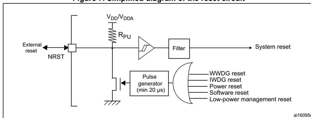
These sources act on the NRST pin and it is always kept low during the delay phase. The RESET service routine vector is fixed at address 0x0000_0004 in the memory map. For more details, refer to Table 51: External interrupt/event controller register map and reset values on page 143 .
The system reset signal provided to the device is output on the NRST pin. The pulse generator guarantees a minimum reset pulse duration of 20 µs for each internal reset source. In case of an external reset, the reset pulse is generated while the NRST pin is asserted low.
Figure 7. Simplified diagram of the reset circuit
6.1.3 Backup domain reset
The backup domain has two specific resets that affect only the backup domain (see Figure 4 ).
A backup domain reset is generated when one of the following events occurs:
- 1. Software reset, triggered by setting the BDRST bit in the Backup domain control register (RCC_BDCR) .
- 2. \( V_{DD} \) or \( V_{BAT} \) power on, if both supplies have previously been powered off.
6.2 Clocks
Three different clock sources can be used to drive the system clock (SYSCLK):
- • HSI oscillator clock
- • HSE oscillator clock
- • PLL clock
The devices have the following two secondary clock sources:
- • 40 kHz low speed internal RC (LSI RC) which drives the independent watchdog and optionally the RTC used for Auto-wakeup from Stop/Standby mode.
- • 32.768 kHz low speed external crystal (LSE crystal) which optionally drives the real-time clock (RTCCLK)
Each clock source can be switched on or off independently when it is not used, to optimize power consumption.
Figure 8. STM32F100xx clock tree (low and medium-density devices)
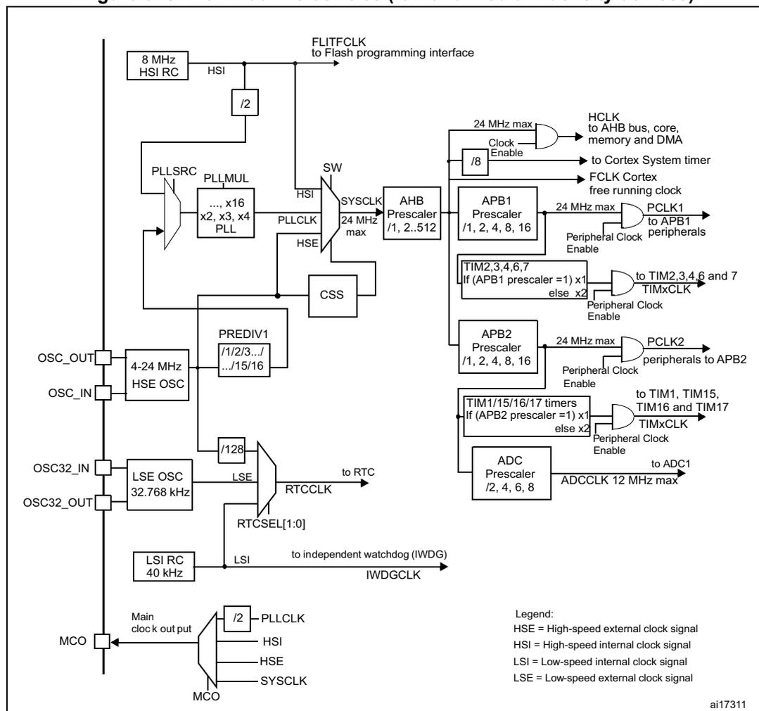
The diagram shows the following clock sources and their paths:
- 8 MHz HSI RC : Connected to the HSI input. It can be divided by 2 (/2) to provide the FLITFCLK to the Flash programming interface.
- 4-24 MHz HSE OSC : Connected to OSC_IN and OSC_OUT pins. It can be divided by PREDIV1 (1/1, 2/3, ..., 15/16) and then fed into the PLL.
- 32.768 kHz LSE OSC : Connected to OSC32_IN and OSC32_OUT pins. It can be divided by 128 and then fed into the RTC.
- 40 kHz LSI RC : Connected to the LSI input. It drives the independent watchdog (IWDG) and optionally the RTC.
The PLL (Phase-Locked Loop) is configured with PLLSRC (selecting HSI or HSE), PLLMUL (x2, x3, x4), and PLLXTPRE (x16). The PLL output (PLLCLK) is fed into the SYSCLK input.
The SYSCLK (System Clock) is selected by a switch (SW) between HSI, PLLCLK, and HSE. It is divided by the AHB Prescaler (1, 2, 2.5, 12) to provide the HCLK to the AHB bus, core, memory, and DMA. It is also divided by 8 to provide the FCLK Cortex free running clock to the Cortex System timer.
The APB1 Prescaler (1, 2, 4, 8, 16) divides the HCLK to provide the PCLK1 to APB1 peripherals. It also provides the TIM2,3,4,6,7 TIMxCLK (if APB1 prescaler = 1) x1 else x2.
The APB2 Prescaler (1, 2, 4, 8, 16) divides the HCLK to provide the PCLK2 to APB2 peripherals. It also provides the TIM1,15,16,17 TIMxCLK (if APB2 prescaler = 1) x1 else x2.
The ADC Prescaler (1/2, 4, 6, 8) divides the HCLK to provide the ADCCLK to the ADC1.
The MCO (Main clock out put) pin can be configured to output the PLLCLK (divided by 2), HSI, HSE, or SYSCLK.
Legend:
- HSE = High-speed external clock signal
- HSI = High-speed internal clock signal
- LSI = Low-speed internal clock signal
- LSE = Low-speed external clock signal
ai17311
- 1. For full details about the internal and external clock source characteristics, refer to the “Electrical characteristics” section in the device datasheet.
Figure 9. STM32F100xx clock tree (high-density devices)
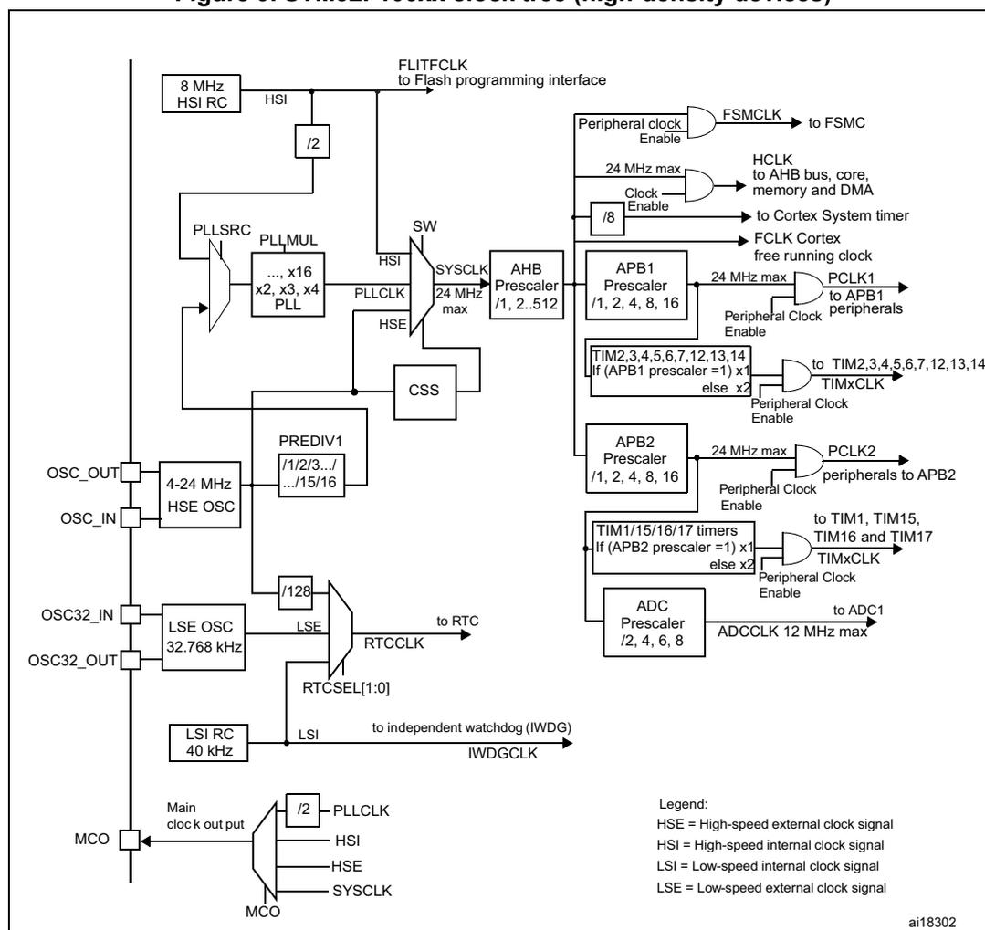
The diagram shows the following clock sources and paths:
- 8 MHz HSI RC : Internal High-Speed Internal clock. It is divided by 2 (/2) to provide FLITFCLK to the Flash programming interface. It also feeds into the PLL (via PLLSRC) and the MCO (Main Clock Output).
- HSE OSC (4-24 MHz): External High-Speed External clock. It is divided by PREDIV1 (options: /1/2/3.../15/16) and then feeds into the PLL (via PLLSRC).
- LSE OSC (32.768 kHz): External Low-Speed External clock. It is divided by /128 and feeds into the RTCCLK for the Real-Time Clock (RTC).
- LSI RC (40 kHz): Internal Low-Speed Internal clock. It feeds into the RTCCLK and the IWDGCLK for the Independent Watchdog (IWDG).
- PLL : Phase-Locked Loop. It takes HSI or HSE (via PLLSRC) as input and multiplies it by PLL_MUL (options: x2, x3, x4). The output is PLLCLK , which feeds into the SW (System Clock Switch) and the MCO .
- SW : System Clock Switch. It selects between HSI, PLLCLK, and HSE to provide the SYSCLK to the AHB Prescaler .
- AHB Prescaler : Divides SYSCLK (options: /1, 2, 5, 12) to provide the HCLK to the AHB bus, core, memory, and DMA. It also feeds into the Cortex System timer (divided by 8) and the FCLK (Cortex free running clock).
- APB1 Prescaler : Divides HCLK (options: /1, 2, 4, 8, 16) to provide the PCLK1 to APB1 peripherals. It also feeds into TIM2,3,4,5,6,7,12,13,14 (if prescaler = 1, then x1; else x2) to provide TIMxCLK .
- APB2 Prescaler : Divides HCLK (options: /1, 2, 4, 8, 16) to provide the PCLK2 to APB2 peripherals. It also feeds into TIM1,15,16,17 (if prescaler = 1, then x1; else x2) to provide TIMxCLK . It also feeds into the ADC Prescaler to provide ADCCLK .
- MCO : Main Clock Output. It can be configured to output PLLCLK, HSI, HSE, or SYSCLK, divided by 2 (/2).
Legend:
- HSE = High-speed external clock signal
- HSI = High-speed internal clock signal
- LSI = Low-speed internal clock signal
- LSE = Low-speed external clock signal
ai18302
Several prescalers allow the configuration of the AHB frequency, the high speed APB (APB2) and the low speed APB (APB1) domains. The maximum frequency of the AHB, APB1 and APB2 domains is 24 MHz.
The RCC feeds the Cortex System Timer (SysTick) external clock with the AHB clock (HCLK) divided by 8. The SysTick can work either with this clock or with the Cortex clock (HCLK), configurable in the SysTick Control and Status Register. ADC1 is clocked by the clock of the High Speed domain (APB2) divided by 2, 4, 6 or 8.
The flash memory programming interface clock (FLITFCLK) is always the HSI clock.
The timer clock frequencies are automatically fixed by hardware. There are two cases:
- 1. if the APB prescaler is 1, the timer clock frequencies are set to the same frequency as that of the APB domain to which the timers are connected.
- 2. otherwise, they are set to twice ( \( \times 2 \) ) the frequency of the APB domain to which the timers are connected.
FCLK acts as Cortex ® -M3 free running clock. For more details refer to the Arm Cortex ® -M3 Technical Reference
Manual. http://infocenter.arm.com/help/topic/com.arm.doc.ddi0337e/DDI0337E_cortex_m3_r1p1_trm.pdf
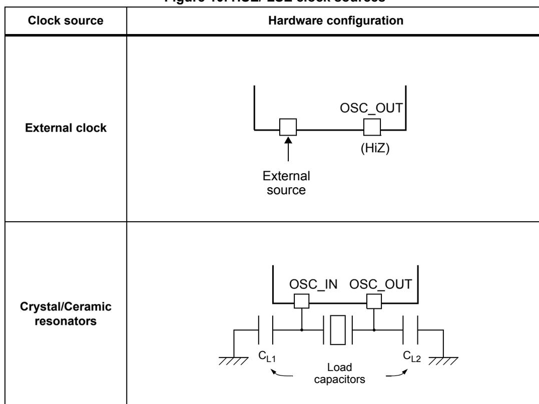
6.2.1 HSE clock
The high speed external clock signal (HSE) can be generated from two possible clock sources:
- • HSE external crystal/ceramic resonator
- • HSE user external clock
The resonator and the load capacitors have to be placed as close as possible to the oscillator pins in order to minimize output distortion and startup stabilization time. The loading capacitance values must be adjusted according to the selected oscillator.
Figure 10. HSE/ LSE clock sources
| Clock source | Hardware configuration |
|---|---|
| External clock | |
| Crystal/Ceramic resonators |
External source (HSE bypass)
In this mode, an external clock source must be provided. It can have a frequency of up to 24 MHz. This mode is selected by setting the HSEBYP and HSEON bits in the Clock control register (RCC_CR) . The external clock signal (square, sinus or triangle) with ~50% duty cycle has to drive the OSC_IN pin while the OSC_OUT pin should be left hi-Z. See Figure 10 .
External crystal/ceramic resonator (HSE crystal)
The 4 to 24 MHz external oscillator has the advantage of producing a very accurate rate on the main clock.
The associated hardware configuration is shown in Figure 10 . Refer to the electrical characteristics section of the datasheet for more details.
The HSERDY flag in the Clock control register (RCC_CR) indicates if the high-speed external oscillator is stable or not. At startup, the clock is not released until this bit is set by hardware. An interrupt can be generated if enabled in the Clock interrupt register (RCC_CIR) .
The HSE Crystal can be switched on and off using the HSEON bit in the Clock control register (RCC_CR) .
6.2.2 HSI clock
The HSI clock signal is generated from an internal 8 MHz RC Oscillator and can be used directly as a system clock or divided by 2 to be used as PLL input.
The HSI RC oscillator has the advantage of providing a clock source at low cost (no external components). It also has a faster startup time than the HSE crystal oscillator however, even with calibration the frequency is less accurate than an external crystal oscillator or ceramic resonator.
Calibration
RC oscillator frequencies can vary from one chip to another due to manufacturing process variations, this is why each device is factory calibrated by ST for 1% accuracy at \( T_A=25^\circ\text{C} \) .
After reset, the factory calibration value is loaded in the HSICAL[7:0] bits in the Clock control register (RCC_CR) .
If the application is subject to voltage or temperature variations this may affect the RC oscillator speed. The HSI frequency can be trimmed in the application using the HSITRIM[4:0] bits in the Clock control register (RCC_CR) .
The HSIRDY flag in the Clock control register (RCC_CR) indicates if the HSI RC is stable or not. At startup, the HSI RC output clock is not released until this bit is set by hardware.
The HSI RC can be switched on and off using the HSION bit in the Clock control register (RCC_CR) .
The HSI signal can also be used as a backup source (Auxiliary clock) if the HSE crystal oscillator fails. Refer to Section 6.2.7: Clock security system (CSS) on page 78 .
6.2.3 PLL
The internal PLL can be used to multiply the HSI RC output or HSE oscillator divided by 1..16 output clock frequency. Refer to Figure 8 and Clock control register (RCC_CR) .
The PLL configuration (selection of HSI oscillator divided by 2 or HSE oscillator for PLL input clock, and multiplication factor) must be done before enabling the PLL. Once the PLL enabled, these parameters cannot be changed.
Note: The PLL output frequency must be in the range of 16-24 MHz.
An interrupt can be generated when the PLL is ready if enabled in the Clock interrupt register (RCC_CIR) .
6.2.4 LSE clock
The LSE crystal is a 32.768 kHz Low Speed External crystal or ceramic resonator. It has the advantage providing a low-power but highly accurate clock source to the real-time clock peripheral (RTC) for clock/calendar or other timing functions.
The LSE crystal is switched on and off using the LSEON bit in Backup domain control register (RCC_BDCR) .
The LSERDY flag in the Backup domain control register (RCC_BDCR) indicates if the LSE crystal is stable or not. At startup, the LSE crystal output clock signal is not released until this bit is set by hardware. An interrupt can be generated if enabled in the Clock interrupt register (RCC_CIR) .
External source (LSE bypass)
In this mode, an external clock source must be provided. It must have a frequency of 32.768 kHz. This mode is selected by setting the LSEBYP and LSEON bits in the Backup domain control register (RCC_BDCR) . The external clock signal (square, sinus or triangle) with ~50% duty cycle has to drive the OSC32_IN pin while the OSC32_OUT pin should be left Hi-Z. See Figure 10 .
6.2.5 LSI clock
The LSI RC acts as an low-power clock source that can be kept running in Stop and Standby mode for the independent watchdog (IWDG) and Auto-wakeup unit (AWU). The clock frequency is around 40 kHz. For more details, refer to the electrical characteristics section of the datasheets.
The LSI RC can be switched on and off using the LSION bit in the Control/status register (RCC_CSR) .
The LSIRDY flag in the Control/status register (RCC_CSR) indicates if the low-speed internal oscillator is stable or not. At startup, the clock is not released until this bit is set by hardware. An interrupt can be generated if enabled in the Clock interrupt register (RCC_CIR) .
LSI calibration
Note: LSI calibration is only available on high-density value line devices.
The frequency dispersion of the Low Speed Internal RC (LSI) oscillator can be calibrated to have accurate RTC time base and/or IWDG timeout (when LSI is used as clock source for these peripherals) with an acceptable accuracy.
This calibration is performed by measuring the LSI clock frequency with respect to TIM5 input clock (TIM5CLK). According to this measurement done at the precision of the HSE oscillator, the software can adjust the programmable 20-bit prescaler of the RTC to get an accurate time base or can compute accurate IWDG timeout.
Use the following procedure to calibrate the LSI:
- 1. Enable TIM5 timer and configure channel4 in input capture mode
- 2. Set the TIM5CH4_IREMAP bit in the AFIO_MAPR register to connect the LSI clock internally to TIM5 channel4 input capture for calibration purposes.
- 3. Measure the frequency of LSI clock using the TIM5 Capture/compare 4 event or interrupt.
- 4. Use the measured LSI frequency to update the 20-bit prescaler of the RTC depending on the desired time base and/or to compute the IWDG timeout.
6.2.6 System clock (SYSCLK) selection
After a system reset, the HSI oscillator is selected as system clock. When a clock source is used directly or through the PLL as system clock, it is not possible to stop it.
A switch from one clock source to another occurs only if the target clock source is ready (clock stable after startup delay or PLL locked). If a clock source which is not yet ready is selected, the switch will occur when the clock source will be ready. Status bits in the Clock control register (RCC_CR) indicate which clock(s) is (are) ready and which clock is currently used as system clock.
6.2.7 Clock security system (CSS)
Clock Security System can be activated by software. In this case, the clock detector is enabled after the HSE oscillator startup delay, and disabled when this oscillator is stopped.
If a failure is detected on the HSE clock, the HSE oscillator is automatically disabled, a clock failure event is sent to the break input of the advanced-control timers (TIM1) and an interrupt is generated to inform the software about the failure (Clock Security System Interrupt CSSI), allowing the MCU to perform rescue operations. The CSSI is linked to the Cortex ® -M3 NMI (Non-Maskable Interrupt) exception vector.
Note: Once the CSS is enabled and if the HSE clock fails, the CSS interrupt occurs and an NMI is automatically generated. The NMI will be executed indefinitely unless the CSS interrupt pending bit is cleared. As a consequence, in the NMI ISR user must clear the CSS interrupt by setting the CSSC bit in the Clock interrupt register (RCC_CIR) .
If the HSE oscillator is used directly or indirectly as the system clock (indirectly means: it is used as PLL input clock, and the PLL clock is used as system clock), a detected failure causes a switch of the system clock to the HSI oscillator and the disabling of the HSE oscillator. If the HSE clock (divided or not) is the clock entry of the PLL used as system clock when the failure occurs, the PLL is disabled too.
6.2.8 RTC clock
The RTCCLK clock source can be either the HSE/128, LSE or LSI clocks. This is selected by programming the RTCSEL[1:0] bits in the Backup domain control register (RCC_BDCR) . This selection cannot be modified without resetting the Backup domain.
The LSE clock is in the Backup domain, whereas the HSE and LSI clocks are not. Consequently:
- • If LSE is selected as RTC clock:
- – The RTC continues to work even if the \( V_{DD} \) supply is switched off, provided the \( V_{BAT} \) supply is maintained.
- • If LSI is selected as Auto-Wakeup unit (AWU) clock:
- – The AWU state is not guaranteed if the \( V_{DD} \) supply is powered off. Refer to Section 6.2.5: LSI clock on page 77 for more details on LSI calibration.
- • If the HSE clock divided by 128 is used as the RTC clock:
- – The RTC state is not guaranteed if the \( V_{DD} \) supply is powered off or if the internal voltage regulator is powered off (removing power from the 1.8 V domain).
- – The DPB bit (Disable backup domain write protection) in the Power controller register must be set to 1 (refer to Section 4.4.1: Power control register (PWR_CR) ).
When the RTC clock is LSE, the RTC remains clocked and functional under system reset.
6.2.9 Watchdog clock
If the Independent watchdog (IWDG) is started by either hardware option or software access, the LSI oscillator is forced ON and cannot be disabled. After the LSI oscillator temporization, the clock is provided to the IWDG.
6.2.10 Clock-out capability
The microcontroller clock output (MCO) capability allows the clock to be output onto the external MCO pin. The configuration registers of the corresponding GPIO port must be programmed in alternate function mode. One of 4 clock signals can be selected as the MCO clock.
- • SYSCLK
- • HSI
- • HSE
- • PLL clock divided by 2
The selection is controlled by the MCO[2:0] bits of the Clock configuration register (RCC_CFGR) .
6.3 RCC registers
Refer to Section 1.1 on page 32 for a list of abbreviations used in register descriptions.
6.3.1 Clock control register (RCC_CR)
Address offset: 0x00
Reset value: 0x0000 XX83 where X is undefined.
Access: no wait state, word, half-word and byte access
| 31 | 30 | 29 | 28 | 27 | 26 | 25 | 24 | 23 | 22 | 21 | 20 | 19 | 18 | 17 | 16 |
|---|---|---|---|---|---|---|---|---|---|---|---|---|---|---|---|
| Reserved | PLL RDY | PLLON | Reserved | CSS ON | HSE BYP | HSE RDY | HSE ON | ||||||||
| r | rw | rw | rw | r | rw | ||||||||||
| 15 | 14 | 13 | 12 | 11 | 10 | 9 | 8 | 7 | 6 | 5 | 4 | 3 | 2 | 1 | 0 |
| HSICAL[7:0] | HSITRIM[4:0] | Res. | HSI RDY | HSION | |||||||||||
| r | r | r | r | r | r | r | r | rw | rw | rw | rw | rw | r | rw | |
Bits 31:26 Reserved, always read as 0.
Bit 25 PLLREADY : PLL clock ready flag
Set by hardware to indicate that the PLL is locked.
0: PLL unlocked
1: PLL locked
Bit 24 PLLON : PLL enable
Set and cleared by software to enable PLL.
Cleared by hardware when entering Stop or Standby mode. This bit can not be reset if the PLL clock is used as system clock or is selected to become the system clock.
0: PLL OFF
1: PLL ON
Bits 23:20 Reserved, always read as 0.
Bit 19 CSSON : Clock security system enable
Set and cleared by software to enable the clock security system. When CSSON is set, the clock detector is enabled by hardware when the HSE oscillator is ready, and disabled by hardware if an HSE clock failure is detected.
0: Clock detector OFF
1: Clock detector ON (Clock detector ON if the HSE oscillator is ready , OFF if not).
Bit 18 HSEBYP : External high-speed clock bypass
Set and cleared by software to bypass the oscillator with an external clock. The external clock must be enabled with the HSEON bit set, to be used by the device. The HSEBYP bit can be written only if the HSE oscillator is disabled.
0: HSE oscillator not bypassed
1: HSE oscillator bypassed with external clock
Bit 17 HSERDY : External high-speed clock ready flag
Set by hardware to indicate that the HSE oscillator is stable. This bit needs 6 cycles of the HSE oscillator clock to go to zero after HSEON is reset.
0: HSE oscillator not ready
1: HSE oscillator ready
Bit 16 HSEON : External high-speed clock enable
Set and cleared by software.
Cleared by hardware to stop the HSE oscillator when entering in Stop or Standby mode. This bit cannot be reset if the HSE oscillator is used directly or indirectly as the system clock.
0: HSE oscillator OFF
1: HSE oscillator ON
Bits 15:8 HSICAL[7:0] : Internal high-speed clock calibration
These bits are initialized automatically at startup.
Bits 7:3 HSITRIM[4:0] : Internal high-speed clock trimming
These bits provide an additional user-programmable trimming value that is added to the HSICAL[7:0] bits. It can be programmed to adjust to variations in voltage and temperature that influence the frequency of the internal HSI RC.
The default value is 16, which, when added to the HSICAL value, should trim the HSI to 8 MHz \( \pm \) 1%. The trimming step ( \( F_{\text{hsitrim}} \) ) is around 40 kHz between two consecutive HSICAL steps.
Bit 2 Reserved, always read as 0.
Bit 1 HSIRDY : Internal high-speed clock ready flag
Set by hardware to indicate that internal 8 MHz RC oscillator is stable. After the HSION bit is cleared, HSIRDY goes low after 6 internal 8 MHz RC oscillator clock cycles.
0: internal 8 MHz RC oscillator not ready
1: internal 8 MHz RC oscillator ready
Bit 0 HSION : Internal high-speed clock enable
Set and cleared by software.
Set by hardware to force the internal 8 MHz RC oscillator ON when leaving Stop or Standby mode or in case of failure of the HSE oscillator used directly or indirectly as system clock.
This bit cannot be reset if the internal 8 MHz RC is used directly or indirectly as system clock or is selected to become the system clock.
0: internal 8 MHz RC oscillator OFF
1: internal 8 MHz RC oscillator ON
6.3.2 Clock configuration register (RCC_CFGR)
Address offset: 0x04
Reset value: 0x0000 0000
Access: \( 0 \leq \text{wait state} \leq 2 \) , word, half-word and byte access
1 or 2 wait states inserted only if the access occurs during clock source switch.
| 31 | 30 | 29 | 28 | 27 | 26 | 25 | 24 | 23 | 22 | 21 | 20 | 19 | 18 | 17 | 16 |
|---|---|---|---|---|---|---|---|---|---|---|---|---|---|---|---|
| Reserved | MCO[2:0] | Reserved | PLLMUL[3:0] | PLL XTPRE | PLL SRC | ||||||||||
| rw | rw | rw | rw | rw | rw | rw | rw | rw | |||||||
| 15 | 14 | 13 | 12 | 11 | 10 | 9 | 8 | 7 | 6 | 5 | 4 | 3 | 2 | 1 | 0 |
| ADC PRE[1:0] | PPRE2[2:0] | PPRE1[2:0] | HPRE[3:0] | SWS[1:0] | SW[1:0] | ||||||||||
| rw | rw | rw | rw | rw | rw | rw | rw | rw | rw | rw | rw | r | r | rw | rw |
Bits 31:27 Reserved, always read as 0.
Bits 26:24
MCO
: Microcontroller clock output
Set and cleared by software.
0xx: No clock
100: System clock (SYSCLK) selected
101: HSI clock selected
110: HSE clock selected
111: PLL clock divided by 2 selected
Note: This clock output may have some truncated cycles at startup or during MCO clock source switching.
Bits 23:22 Reserved.
Bits 21:18
PLLMUL
: PLL multiplication factor
These bits are written by software to define the PLL multiplication factor. These bits can be written only when PLL is disabled.
Caution: The PLL output frequency must be in the 16-24 MHz range.
0000: PLL input clock x 2
0001: PLL input clock x 3
0010: PLL input clock x 4
0011: PLL input clock x 5
0100: PLL input clock x 6
0101: PLL input clock x 7
0110: PLL input clock x 8
0111: PLL input clock x 9
1000: PLL input clock x 10
1001: PLL input clock x 11
1010: PLL input clock x 12
1011: PLL input clock x 13
1100: PLL input clock x 14
1101: PLL input clock x 15
1110: PLL input clock x 16
1111: PLL input clock x 16
Set and cleared by software to select the least significant bit of the PREDIV1 division factor. It is the same bit as bit 0 in the RCC_CFGR2 register, so modifying bit 0 in the RCC_CFGR2 register changes this bit accordingly.
If bits[3:1] in the RCC_CFGR2 register are not set, the PLLXTPRE bit controls if PREDIV1 divides its input clock by 2 (PLLXTPRE=1) or not (PLLXTPRE=0).
This bit can be written only when the PLL is disabled.
Bit 16 PLLSRC: PLL entry clock sourceSet and cleared by software to select PLL clock source. This bit can be written only when PLL is disabled.
0: HSI oscillator clock / 2 selected as PLL input clock
1: Clock from PREDIV1 selected as the PLL input clock
Bits 15:14 ADCPRE: ADC prescalerSet and cleared by software to select the frequency of the clock to ADC1.
00: PLCK2 divided by 2
01: PLCK2 divided by 4
10: PLCK2 divided by 6
11: PLCK2 divided by 8
Bits 13:11 PPRE2: APB high-speed prescaler (APB2)Set and cleared by software to control the division factor of the APB high-speed clock (PCLK2).
0xx: HCLK not divided
100: HCLK divided by 2
101: HCLK divided by 4
110: HCLK divided by 8
111: HCLK divided by 16
Bits 10:8 PPRE1: APB low-speed prescaler (APB1)Set and cleared by software to control the division factor of the APB low-speed clock (PCLK1).
Warning: the software has to set correctly these bits to not exceed 36 MHz on this domain.
0xx: HCLK not divided
100: HCLK divided by 2
101: HCLK divided by 4
110: HCLK divided by 8
111: HCLK divided by 16
Bits 7:4 HPRE: AHB prescalerSet and cleared by software to control the division factor of the AHB clock.
0xxx: SYSCLK not divided
1000: SYSCLK divided by 2
1001: SYSCLK divided by 4
1010: SYSCLK divided by 8
1011: SYSCLK divided by 16
1100: SYSCLK divided by 64
1101: SYSCLK divided by 128
1110: SYSCLK divided by 256
1111: SYSCLK divided by 512
Bits 3:2 SWS : System clock switch status
Set and cleared by hardware to indicate which clock source is used as system clock.
00: HSI oscillator used as system clock
01: HSE oscillator used as system clock
10: PLL used as system clock
11: not applicable
Bits 1:0 SW : System clock switch
Set and cleared by software to select SYSCLK source.
Set by hardware to force HSI selection when leaving Stop and Standby mode or in case of failure of the HSE oscillator used directly or indirectly as system clock (if the Clock Security System is enabled).
00: HSI selected as system clock
01: HSE selected as system clock
10: PLL selected as system clock
11: not allowed
6.3.3 Clock interrupt register (RCC_CIR)
Address offset: 0x08
Reset value: 0x0000 0000
Access: no wait state, word, half-word and byte access
| 31 | 30 | 29 | 28 | 27 | 26 | 25 | 24 | 23 | 22 | 21 | 20 | 19 | 18 | 17 | 16 |
|---|---|---|---|---|---|---|---|---|---|---|---|---|---|---|---|
| Reserved | CSSC | Reserved | PLL RDYC | HSE RDYC | HSI RDYC | LSE RDYC | LSI RDYC | ||||||||
| w | w | w | w | w | w | ||||||||||
| 15 | 14 | 13 | 12 | 11 | 10 | 9 | 8 | 7 | 6 | 5 | 4 | 3 | 2 | 1 | 0 |
| Reserved | PLL RDYIE | HSE RDYIE | HSI RDYIE | LSE RDYIE | LSI RDYIE | CSSF | Reserved | PLL RDYF | HSE RDYF | HSI RDYF | LSE RDYF | LSI RDYF | |||
| r/w | r/w | r/w | r/w | r/w | r | r | r | r | r | r | |||||
Bits 31:24 Reserved, always read as 0.
Bit 23 CSSC : Clock security system interrupt clear
This bit is set by software to clear the CSSF flag.
0: No effect
1: Clear CSSF flag
Bits 22:21 Reserved, always read as 0.
Bit 20 PLLRDYC : PLL ready interrupt clear
This bit is set by software to clear the PLLRDYF flag.
0: No effect
1: PLLRDYF cleared
Bit 19 HSERDYC : HSE ready interrupt clear
This bit is set by software to clear the HSERDYF flag.
0: No effect
1: HSERDYF cleared
- Bit 18
HSIRDYC
: HSI ready interrupt clear
This bit is set software to clear the HSIRDYF flag.
0: No effect
1: HSIRDYF cleared - Bit 17
LSERDYC
: LSE ready interrupt clear
This bit is set by software to clear the LSERDYF flag.
0: No effect
1: LSERDYF cleared - Bit 16
LSIRDYC
: LSI ready interrupt clear
This bit is set by software to clear the LSIRDYF flag.
0: No effect
1: LSIRDYF cleared - Bits 15:13 Reserved, always read as 0.
- Bit 12
PLLRDYIE
: PLL ready interrupt enable
Set and cleared by software to enable/disable interrupt caused by PLL lock.
0: PLL lock interrupt disabled
1: PLL lock interrupt enabled - Bit 11
HSERDYIE
: HSE ready interrupt enable
Set and cleared by software to enable/disable interrupt caused by the HSE oscillator stabilization.
0: HSE ready interrupt disabled
1: HSE ready interrupt enabled - Bit 10
HSIRDYIE
: HSI ready interrupt enable
Set and cleared by software to enable/disable interrupt caused by the internal 8 MHz RC oscillator stabilization.
0: HSI ready interrupt disabled
1: HSI ready interrupt enabled - Bit 9
LSERDYIE
: LSE ready interrupt enable
Set and cleared by software to enable/disable interrupt caused by the external 32 kHz oscillator stabilization.
0: LSE ready interrupt disabled
1: LSE ready interrupt enabled - Bit 8
LSIRDYIE
: LSI ready interrupt enable
Set and cleared by software to enable/disable interrupt caused by internal RC 40 kHz oscillator stabilization.
0: LSI ready interrupt disabled
1: LSI ready interrupt enabled - Bit 7
CSSF
: Clock security system interrupt flag
Set by hardware when a failure is detected in the HSE oscillator.
Cleared by software setting the CSSC bit.
0: No clock security interrupt caused by HSE clock failure
1: Clock security interrupt caused by HSE clock failure - Bits 6:5 Reserved, always read as 0.
Bit 4 PLLREADYF : PLL ready interrupt flag
Set by hardware when the PLL locks and PLLRDYDIE is set.
Cleared by software setting the PLLRDYIC bit.
0: No clock ready interrupt caused by PLL lock
1: Clock ready interrupt caused by PLL lockBit3 HSERDYF : HSE ready interrupt flag
Set by hardware when External High Speed clock becomes stable and HSERDYDIE is set.
Cleared by software setting the HSERDYIC bit.
0: No clock ready interrupt caused by the HSE oscillator
1: Clock ready interrupt caused by the HSE oscillatorBit 2 HSIRDYF : HSI ready interrupt flag
Set by hardware when the Internal High Speed clock becomes stable and HSIRDYDIE is set.
Cleared by software setting the HSIRDYIC bit.
0: No clock ready interrupt caused by the internal 8 MHz RC oscillator
1: Clock ready interrupt caused by the internal 8 MHz RC oscillatorBit 1 LSERDYF : LSE ready interrupt flag
Set by hardware when the External Low Speed clock becomes stable and LSERDYDIE is set.
Cleared by software setting the LSERDYIC bit.
0: No clock ready interrupt caused by the external 32 kHz oscillator
1: Clock ready interrupt caused by the external 32 kHz oscillatorBit 0 LSIRDYF : LSI ready interrupt flag
Set by hardware when the internal low speed clock becomes stable and LSIRDYDIE is set.
Cleared by software setting the LSIRDYIC bit.
0: No clock ready interrupt caused by the internal RC 40 kHz oscillator
1: Clock ready interrupt caused by the internal RC 40 kHz oscillator
6.3.4 APB2 peripheral reset register (RCC_APB2RSTR)
Address offset: 0x0C
Reset value: 0x00000 0000
Access: no wait state, word, half-word and byte access
| 31 | 30 | 29 | 28 | 27 | 26 | 25 | 24 | 23 | 22 | 21 | 20 | 19 | 18 | 17 | 16 |
|---|---|---|---|---|---|---|---|---|---|---|---|---|---|---|---|
| Reserved | TIM17 RST | TIM16 RST | TIM15 RST | ||||||||||||
| rw | rw | rw | |||||||||||||
| 15 | 14 | 13 | 12 | 11 | 10 | 9 | 8 | 7 | 6 | 5 | 4 | 3 | 2 | 1 | 0 |
| Res. | USART1 RST | Res. | SPI1 RST | TIM1 RST | Res. | ADC1 RST | IOPG RST | IOPF RST | IOPD RST | IOPC RST | IOPB RST | IOPA RST | Res. | Res. | AFIO RST |
| rw | rw | rw | rw | rw | rw | rw | rw | rw | rw | Res. | rw | ||||
Bits 31:19 Reserved, always read as 0.
- Bit 18
TIM17RST
: TIM17 reset
Set and cleared by software.
0: No effect
1: Reset TIM17 - Bit 17
TIM16RST
: TIM16 reset
Set and cleared by software.
0: No effect
1: Resets TIM16 - Bit 16
TIM15RST
: TIM15 reset
Set and cleared by software.
0: No effect
1: Resets TIM15 - Bit 15 Reserved.
- Bit 14
USART1RST
: USART1 reset
Set and cleared by software.
0: No effect
1: Reset USART1 - Bit 13 Reserved.
- Bit 12
SPI1RST
: SPI 1 reset
Set and cleared by software.
0: No effect
1: Reset SPI 1 - Bit 11
TIM1RST
: TIM1 timer reset
Set and cleared by software.
0: No effect
1: Reset TIM1 timer - Bit 10 Reserved.
- Bit 9
ADC1RST
: ADC 1 interface reset
Set and cleared by software.
0: No effect
1: Reset ADC 1 interface - Bit 8
IOPGRST
: IO port G reset
Set and cleared by software.
0: No effect
1: Reset IO port G - Bit 7
IOPFRST
: IO port F reset
Set and cleared by software.
0: No effect
1: Reset I/O port F - Bit 6
IOPERST
: IO port E reset
Set and cleared by software.
0: No effect
1: Reset IO port E
- Bit 5
IOPDRST
: IO port D reset
Set and cleared by software.
0: No effect
1: Reset I/O port D - Bit 4
IOPCRST
: IO port C reset
Set and cleared by software.
0: No effect
1: Reset I/O port C - Bit 3
IOPBRST
: IO port B reset
Set and cleared by software.
0: No effect
1: Reset I/O port B - Bit 2
IOPARST
: I/O port A reset
Set and cleared by software.
0: No effect
1: Reset I/O port A - Bit 1 Reserved, always read as 0.
- Bit 0
AFIORST
: Alternate function I/O reset
Set and cleared by software.
0: No effect
1: Reset Alternate Function
6.3.5 APB1 peripheral reset register (RCC_APB1RSTR)
Address offset: 0x10
Reset value: 0x0000 0000
Access: no wait state, word, half-word and byte access
| 31 | 30 | 29 | 28 | 27 | 26 | 25 | 24 | 23 | 22 | 21 | 20 | 19 | 18 | 17 | 16 |
|---|---|---|---|---|---|---|---|---|---|---|---|---|---|---|---|
| Res. | CECR ST | DAC RST | PWR RST | BKP RST | Reserved | I2C2 RST | I2C1 RST | UART5 RST | |||||||
| rw | rw | rw | rw | rw | rw | rw | |||||||||
| 15 | 14 | 13 | 12 | 11 | 10 | 9 | 8 | 7 | 6 | 5 | 4 | 3 | 2 | 1 | 0 |
| SPI3 RST | SPI2 RST | Reserved | WWDG RST | Reserved | TIM14 RST | TIM13 RST | TIM12 RST | TIM7 RST | TIM6 RST | TIM5 RST | TIM4 RST | TIM3 RST | |||
| rw | rw | rw | rw | rw | rw | rw | rw | rw | rw | TIM2 RST | |||||
| rw | |||||||||||||||
- Bit 31 Reserved, always read as 0.
- Bit 30
CECRST
: CEC reset
Set and cleared by software.
0: No effect
1: Reset CEC - Bit 29
DACRST
: DAC interface reset
Set and cleared by software.
0: No effect
1: Reset DAC interface
- Bit 28
PWRRST
: Power interface reset
Set and cleared by software.
0: No effect
1: Reset power interface - Bit 27
BKPRST
: Backup interface reset
Set and cleared by software.
0: No effect
1: Reset backup interface - Bits 26:23 Reserved, always read as 0.
- Bit 22
I2C2RST
: I2C 2 reset
Set and cleared by software.
0: No effect
1: Reset I2C 2 - Bit 21
I2C1RST
: I2C 1 reset
Set and cleared by software.
0: No effect
1: Reset I2C 1 - Bit 20
UART5RST
: UART 5 reset
Set and cleared by software.
0: No effect
1: Reset UART 5 - Bit 19
UART4RST
: UART 4 reset
Set and cleared by software.
0: No effect
1: Reset UART 4 - Bit 18
USART3RST
: USART 3 reset
Set and cleared by software.
0: No effect
1: Reset USART 3 - Bit 17
USART2RST
: USART 2 reset
Set and cleared by software.
0: No effect
1: Reset USART 2 - Bit 16 Reserved, always read as 0.
- Bit 15
SPI3RST
: SPI 3 reset
Set and cleared by software.
0: No effect
1: Reset SPI 3 - Bit 14
SPI2RST
: SPI 2 reset
Set and cleared by software.
0: No effect
1: Reset SPI 2 - Bits 13:12 Reserved, always read as 0.
- Bit 11
WWDGRST
: Window watchdog reset
Set and cleared by software.
0: No effect
1: Reset window watchdog - Bits 10:9 Reserved, always read as 0.
- Bit 8
TIM14RST
: Timer 14 reset
Set and cleared by software.
0: No effect
1: Reset timer 14 - Bit 7
TIM13RST
: Timer 13 reset
Set and cleared by software.
0: No effect
1: Reset timer 13 - Bit 6
TIM12RST
: Timer 12 reset
Set and cleared by software.
0: No effect
1: Reset timer 12 - Bit 5
TIM7RST
: Timer 7 reset
Set and cleared by software.
0: No effect
1: Reset timer 7 - Bit 4
TIM6RST
: Timer 6 reset
Set and cleared by software.
0: No effect
1: Reset timer 6 - Bit 3
TIM5RST
: Timer 5 reset
Set and cleared by software.
0: No effect
1: Reset timer 5 - Bit 2
TIM4RST
: Timer 4 reset
Set and cleared by software.
0: No effect
1: Reset timer 4 - Bit 1
TIM3RST
: Timer 3 reset
Set and cleared by software.
0: No effect
1: Reset timer 3 - Bit 0
TIM2RST
: Timer 2 reset
Set and cleared by software.
0: No effect
1: Reset timer 2
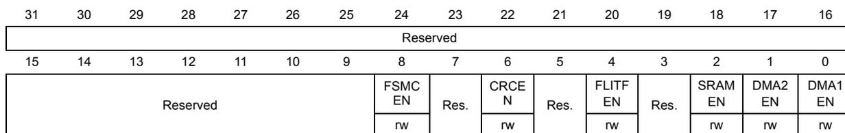
6.3.6 AHB peripheral clock enable register (RCC_AHBENR)
Address offset: 0x14
Reset value: 0x0000 0014
Access: no wait state, word, half-word and byte access
Note: When the peripheral clock is not active, the peripheral register values may not be readable by software and the returned value is always 0x0.
| 31 | 30 | 29 | 28 | 27 | 26 | 25 | 24 | 23 | 22 | 21 | 20 | 19 | 18 | 17 | 16 | |
| Reserved | ||||||||||||||||
| 15 | 14 | 13 | 12 | 11 | 10 | 9 | 8 | 7 | 6 | 5 | 4 | 3 | 2 | 1 | 0 | |
| Reserved | FSMC EN | Res. | CRCE N | Res. | FLITF EN | Res. | SRAM EN | DMA2 EN | DMA1 EN | |||||||
| rw | rw | rw | rw | rw | rw | |||||||||||
Bits 31:9 Reserved, always read as 0.
Bit 8 FSMCEN : FSMC clock enable
Set and cleared by software.
0: FSMC clock disabled
1: FSMC clock enabled
Bit 7 Reserved, always read as 0.
Bit 6 CRCE : CRC clock enable
Set and cleared by software.
0: CRC clock disabled
1: CRC clock enabled
Bit 5 Reserved, always read as 0.
Bit 4 FLITFEN : FLITF clock enable
Set and cleared by software to disable/enable FLITF clock during sleep mode.
0: FLITF clock disabled during Sleep mode
1: FLITF clock enabled during Sleep mode
Bit 3 Reserved, always read as 0.
Bit 2 SRAMEN : SRAM interface clock enable
Set and cleared by software to disable/enable SRAM interface clock during Sleep mode.
0: SRAM interface clock disabled during Sleep mode.
1: SRAM interface clock enabled during Sleep mode
Bit 1 DMA2EN : DMA2 clock enable
Set and cleared by software.
0: DMA2 clock disabled
1: DMA2 clock enabled
Bit 0 DMA1EN : DMA1 clock enable
Set and cleared by software.
0: DMA1 clock disabled
1: DMA1 clock enabled
6.3.7 APB2 peripheral clock enable register (RCC_APB2ENR)
Address: 0x18
Reset value: 0x0000 0000
Access: word, half-word and byte access
No wait states, except if the access occurs while an access to a peripheral in the APB2 domain is on going. In this case, wait states are inserted until the access to APB2 peripheral is finished.
Note: When the peripheral clock is not active, the peripheral register values may not be readable by software and the returned value is always 0x0.
| 31 | 30 | 29 | 28 | 27 | 26 | 25 | 24 | 23 | 22 | 21 | 20 | 19 | 18 | 17 | 16 |
|---|---|---|---|---|---|---|---|---|---|---|---|---|---|---|---|
| Reserved | TIM17 EN | TIM16 EN | TIM15 EN | ||||||||||||
| rw | rw | rw | |||||||||||||
| 15 | 14 | 13 | 12 | 11 | 10 | 9 | 8 | 7 | 6 | 5 | 4 | 3 | 2 | 1 | 0 |
| Res. | USART1 EN | Res. | SPI1 EN | TIM1 EN | Res. | ADC1 EN | IOPG EN | IOPF EN | IOPE EN | IOPD EN | IOPC EN | IOPB EN | IOPA EN | Res. | AFIO EN |
| rw | rw | rw | rw | rw | rw | rw | rw | rw | rw | rw | rw | ||||
Bits 31:19 Reserved, always read as 0.
Bit 18 TIM17EN : TIM17 Timer clock enable
Set and cleared by software.
0: TIM17 timer clock disabled
1: TIM17 timer clock enabled
Bit 17 TIM16EN : TIM16 timer clock enable
Set and cleared by software.
0: TIM16 timer clock disabled
1: TIM16 timer clock enabled
Bit 16 TIM15EN : TIM15 timer clock enable
Set and cleared by software.
0: TIM15 timer clock disabled
1: TIM15 timer clock enabled
Bit 15 Reserved.
Bit 14 USART1EN : USART1 clock enable
Set and cleared by software.
0: USART1 clock disabled
1: USART1 clock enabled
Bit 13 Reserved.
Bit 12 SPI1EN : SPI 1 clock enable
Set and cleared by software.
0: SPI 1 clock disabled
1: SPI 1 clock enabled
- Bit 11
TIM1EN
: TIM1 Timer clock enable
Set and cleared by software.
0: TIM1 timer clock disabled
1: TIM1 timer clock enabled - Bit 10 Reserved.
- Bit 9
ADC1EN
: ADC 1 interface clock enable
Set and cleared by software.
0: ADC 1 interface disabled
1: ADC 1 interface clock enabled - Bit 8
IOPGEN
: I/O port G clock enable
Set and cleared by software.
0: I/O port G clock disabled
1: I/O port G clock enabled - Bit 7
IOPFEN
: I/O port F clock enable
Set and cleared by software.
0: I/O port F clock disabled
1: I/O port F clock enabled - Bit 6
IOPPEN
: I/O port E clock enable
Set and cleared by software.
0: I/O port E clock disabled
1: I/O port E clock enabled - Bit 5
IOPDEN
: I/O port D clock enable
Set and cleared by software.
0: I/O port D clock disabled
1: I/O port D clock enabled - Bit 4
IOPCEN
: I/O port C clock enable
Set and cleared by software.
0: I/O port C clock disabled
1: I/O port C clock enabled - Bit 3
IOPBEN
: I/O port B clock enable
Set and cleared by software.
0: I/O port B clock disabled
1: I/O port B clock enabled - Bit 2
IOPAEN
: I/O port A clock enable
Set and cleared by software.
0: I/O port A clock disabled
1: I/O port A clock enabled - Bit 1 Reserved, always read as 0.
- Bit 0
AFIOEN
: Alternate function I/O clock enable
Set and cleared by software.
0: Alternate Function I/O clock disabled
1: Alternate Function I/O clock enabled
6.3.8 APB1 peripheral clock enable register (RCC_APB1ENR)
Address: 0x1C
Reset value: 0x0000 0000
Access: word, half-word and byte access
No wait state, except if the access occurs while an access to a peripheral on APB1 domain is on going. In this case, wait states are inserted until this access to APB1 peripheral is finished.
Note: When the peripheral clock is not active, the peripheral register values may not be readable by software and the returned value is always 0x0.
| 31 | 30 | 29 | 28 | 27 | 26 | 25 | 24 | 23 | 22 | 21 | 20 | 19 | 18 | 17 | 16 |
|---|---|---|---|---|---|---|---|---|---|---|---|---|---|---|---|
| Res. | CECE N | DAC EN | PWR EN | BKP EN | Reserved | I2C2 EN | I2C1 EN | UART5E N | UART4E N | USART 3EN | USART 2EN | ||||
| rw | rw | rw | rw | rw | rw | rw | rw | rw | Res. | ||||||
| 15 | 14 | 13 | 12 | 11 | 10 | 9 | 8 | 7 | 6 | 5 | 4 | 3 | 2 | 1 | 0 |
| SPI3 EN | SPI2 EN | Reserved | WWD GEN | Reserved | TIM14 EN | TIM13 EN | TIM12 EN | TIM7 EN | TIM6 EN | TIM5 EN | TIM4 EN | TIM3 EN | |||
| rw | rw | rw | rw | rw | rw | rw | rw | rw | rw | TIM2 EN | |||||
Bits 31:29 Reserved, always read as 0.
Bit 30 CECEN : CEC clock enable
Set and cleared by software.
0: CEC clock disabled
1: CEC clock enabled
Bit 29 DACEN : DAC interface clock enable
Set and cleared by software.
0: DAC interface clock disabled
1: DAC interface clock enable
Bit 28 PWREN : Power interface clock enable
Set and cleared by software.
0: Power interface clock disabled
1: Power interface clock enable
Bit 27 BKPEN : Backup interface clock enable
Set and cleared by software.
0: Backup interface clock disabled
1: Backup interface clock enabled
Bits 26:23 Reserved, always read as 0.
Bit 22 I2C2EN : I2C 2 clock enable
Set and cleared by software.
0: I2C 2 clock disabled
1: I2C 2 clock enabled
- Bit 21
I2C1EN
: I2C 1 clock enable
Set and cleared by software.
0: I2C 1 clock disabled
1: I2C 1 clock enabled - Bit 20
UART5EN
: UART 5 clock enable
Set and cleared by software.
0: UART 5 clock disabled
1: UART 5 clock enabled - Bit 19
UART4EN
: UART 4 clock enable
Set and cleared by software.
0: UART 4 clock disabled
1: UART 4 clock enabled - Bit 18
USART3EN
: USART 3 clock enable
Set and cleared by software.
0: USART 3 clock disabled
1: USART 3 clock enabled - Bit 17
USART2EN
: USART 2 clock enable
Set and cleared by software.
0: USART 2 clock disabled
1: USART 2 clock enabled - Bits 16 Reserved, always read as 0.
- Bit 15
SPI3EN
: SPI 3 clock enable
Set and cleared by software.
0: SPI 3 clock disabled
1: SPI 3 clock enabled - Bit 14
SPI2EN
: SPI 2 clock enable
Set and cleared by software.
0: SPI 2 clock disabled
1: SPI 2 clock enabled - Bits 13:12 Reserved, always read as 0.
- Bit 11
WWDGEN
: Window watchdog clock enable
Set and cleared by software.
0: Window watchdog clock disabled
1: Window watchdog clock enabled - Bits 10:9 Reserved, always read as 0.
- Bit 8
TIM14EN
: Timer 14 clock enable
Set and cleared by software.
0: Timer 14 clock disabled
1: Timer 14 clock enabled - Bit 7
TIM13EN
: Timer 13 clock enable
Set and cleared by software.
0: Timer 13 clock disabled
1: Timer 13 clock enabled
- Bit 6
TIM12EN
: Timer 12 clock enable
Set and cleared by software.
0: Timer 12 clock disabled
1: Timer 12 clock enabled - Bit 5
TIM7EN
: Timer 7 clock enable
Set and cleared by software.
0: Timer 7 clock disabled
1: Timer 7 clock enabled - Bit 4
TIM6EN
: Timer 6 clock enable
Set and cleared by software.
0: Timer 6 clock disabled
1: Timer 6 clock enabled - Bit 3
TIM5EN
: Timer 5 clock enable
Set and cleared by software.
0: Timer 5 clock disabled
1: Timer 5 clock enabled - Bit 2
TIM4EN
: Timer 4 clock enable
Set and cleared by software.
0: Timer 4 clock disabled
1: Timer 4 clock enabled - Bit 1
TIM3EN
: Timer 3 clock enable
Set and cleared by software.
0: Timer 3 clock disabled
1: Timer 3 clock enabled - Bit 0
TIM2EN
: Timer 2 clock enable
Set and cleared by software.
0: Timer 2 clock disabled
1: Timer 2 clock enabled
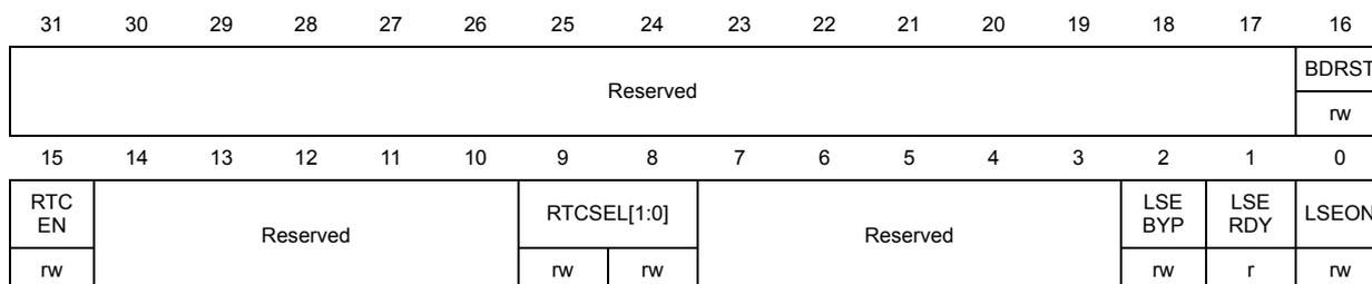
6.3.9 Backup domain control register (RCC_BDCR)
Address offset: 0x20
Reset value: 0x0000 0000, reset by Backup domain Reset.
Access: 0 ≤ wait state ≤ 3, word, half-word and byte access
Wait states are inserted in case of successive accesses to this register.
Note: LSEON, LSEBYP, RTCSEL and RTCEN bits of the Backup domain control register (RCC_BDCR) are in the Backup domain. As a result, after Reset, these bits are write-protected and the DBP bit in the Power control register (PWR_CR) has to be set before these can be modified. Refer to Section 5: Backup registers (BKP) for further information. These bits are only reset after a Backup domain Reset (see Section 6.1.3: Backup domain reset). Any internal or external Reset will not have any effect on these bits.
| 31 | 30 | 29 | 28 | 27 | 26 | 25 | 24 | 23 | 22 | 21 | 20 | 19 | 18 | 17 | 16 |
| Reserved | BDRST | ||||||||||||||
| rw | |||||||||||||||
| 15 | 14 | 13 | 12 | 11 | 10 | 9 | 8 | 7 | 6 | 5 | 4 | 3 | 2 | 1 | 0 |
| RTCEN | Reserved | RTCSEL[1:0] | Reserved | LSEBYP | LSE RDY | LSEON | |||||||||
| rw | rw | rw | r | rw | |||||||||||
Bits 31:17 Reserved, always read as 0.
Bit 16 BDRST : Backup domain software reset
Set and cleared by software.
0: Reset not activated
1: Resets the entire Backup domain
Bit 15 RTCEN : RTC clock enable
Set and cleared by software.
0: RTC clock disabled
1: RTC clock enabled
Bits 14:10 Reserved, always read as 0.
Bits 9:8 RTCSEL[1:0] : RTC clock source selection
Set by software to select the clock source for the RTC. Once the RTC clock source has been selected, it cannot be changed anymore unless the Backup domain is reset. The BDRST bit can be used to reset them.
00: No clock
01: LSE oscillator clock used as RTC clock
10: LSI oscillator clock used as RTC clock
11: HSE oscillator clock divided by 128 used as RTC clock
Bits 7:3 Reserved, always read as 0.
Bit 2 LSEBYP : External low-speed oscillator bypass
Set and cleared by software to bypass oscillator in debug mode. This bit can be written only when the external 32 kHz oscillator is disabled.
0: LSE oscillator not bypassed
1: LSE oscillator bypassed
Bit 1 LSERDY : External low-speed oscillator ready
Set and cleared by hardware to indicate when the external 32 kHz oscillator is stable. After the LSEON bit is cleared, LSERDY goes low after 6 external low-speed oscillator clock cycles.
0: External 32 kHz oscillator not ready
1: External 32 kHz oscillator ready
Bit 0 LSEON : External low-speed oscillator enable
Set and cleared by software.
0: External 32 kHz oscillator OFF
1: External 32 kHz oscillator ON
6.3.10 Control/status register (RCC_CSR)
Address: 0x24
Reset value: 0x0C00 0000, reset by system Reset, except reset flags by power Reset only.
Access: \( 0 \leq \text{wait state} \leq 3 \) , word, half-word and byte access
Wait states are inserted in case of successive accesses to this register.
| 31 | 30 | 29 | 28 | 27 | 26 | 25 | 24 | 23 | 22 | 21 | 20 | 19 | 18 | 17 | 16 |
|---|---|---|---|---|---|---|---|---|---|---|---|---|---|---|---|
| LPWR RSTF | WWDG RSTF | IWDG RSTF | SFT RSTF | POR RSTF | PIN RSTF | Res. | RMVF | Reserved | |||||||
| rw | rw | rw | rw | rw | rw | rw | |||||||||
| 15 | 14 | 13 | 12 | 11 | 10 | 9 | 8 | 7 | 6 | 5 | 4 | 3 | 2 | 1 | 0 |
|---|---|---|---|---|---|---|---|---|---|---|---|---|---|---|---|
| Reserved | LSI RDY | LSION | |||||||||||||
| r | rw | ||||||||||||||
Bit 31 LPWRRSTF : Low-power reset flag
Set by hardware when a Low-power management reset occurs.
Cleared by writing to the RMVF bit.
0: No Low-power management reset occurred
1: Low-power management reset occurred
For further information on Low-power management reset, refer to Low-power management reset .
Bit 30 WWDGRSTF : Window watchdog reset flag
Set by hardware when a window watchdog reset occurs.
Cleared by writing to the RMVF bit.
0: No window watchdog reset occurred
1: Window watchdog reset occurred
Bit 29 IWDGRSTF : Independent watchdog reset flag
Set by hardware when an independent watchdog reset from V DD domain occurs.
Cleared by writing to the RMVF bit.
0: No watchdog reset occurred
1: Watchdog reset occurred
- Bit 28
SFTRSTF
: Software reset flag
Set by hardware when a software reset occurs.
Cleared by writing to the RMVF bit.
0: No software reset occurred
1: Software reset occurred - Bit 27
PORRSTF
: POR/PDR reset flag
Set by hardware when a POR/PDR reset occurs.
Cleared by writing to the RMVF bit.
0: No POR/PDR reset occurred
1: POR/PDR reset occurred - Bit 26
PINRSTF
: PIN reset flag
Set by hardware when a reset from the NRST pin occurs.
Cleared by writing to the RMVF bit.
0: No reset from NRST pin occurred
1: Reset from NRST pin occurred - Bit 25 Reserved, always read as 0.
- Bit 24
RMVF
: Remove reset flag
Set by software to clear the reset flags.
0: No effect
1: Clear the reset flags - Bits 23:2 Reserved, always read as 0.
- Bit 1
LSIRDY
: Internal low-speed oscillator ready
Set and cleared by hardware to indicate when the internal RC 40 kHz oscillator is stable.
After the LSION bit is cleared, LSIRDY goes low after 3 internal RC 40 kHz oscillator clock cycles.
0: Internal RC 40 kHz oscillator not ready
1: Internal RC 40 kHz oscillator ready - Bit 0
LSION
: Internal low-speed oscillator enable
Set and cleared by software.
0: Internal RC 40 kHz oscillator OFF
1: Internal RC 40 kHz oscillator ON
6.3.11 Clock configuration register2 (RCC_CFGR2)
Address offset: 0x2C
Access: no wait state, word, half-word and byte access
Reset value: 0x0000 0000
| 31 | 30 | 29 | 28 | 27 | 26 | 25 | 24 | 23 | 22 | 21 | 20 | 19 | 18 | 17 | 16 |
| Reserved | |||||||||||||||
| 15 | 14 | 13 | 12 | 11 | 10 | 9 | 8 | 7 | 6 | 5 | 4 | 3 | 2 | 1 | 0 |
| Reserved | PREDIV1[3:0] | ||||||||||||||
| rw | rw | rw | rw | ||||||||||||
Bits 31:4 Reserved.
Bits 3:0 PREDIV1[3:0] : PREDIV1 division factor
Set and cleared by software to select the PREDIV1 division factor. These bits can be written only when the PLL is disabled.
Note: Bit 0 is the same as bit 17 in the RCC_CFGR register, so modifying bit 17 in the RCC_CFGR register changes bit 0 accordingly.
- 0000: PREDIV1 input clock not divided
- 0001: PREDIV1 input clock divided by 2
- 0010: PREDIV1 input clock divided by 3
- 0011: PREDIV1 input clock divided by 4
- 0100: PREDIV1 input clock divided by 5
- 0101: PREDIV1 input clock divided by 6
- 0110: PREDIV1 input clock divided by 7
- 0111: PREDIV1 input clock divided by 8
- 1000: PREDIV1 input clock divided by 9
- 1001: PREDIV1 input clock divided by 10
- 1010: PREDIV1 input clock divided by 11
- 1011: PREDIV1 input clock divided by 12
- 1100: PREDIV1 input clock divided by 13
- 1101: PREDIV1 input clock divided by 14
- 1110: PREDIV1 input clock divided by 15
- 1111: PREDIV1 input clock divided by 16
6.3.12 RCC register map
The following table gives the RCC register map and the reset values.
Table 15. RCC register map and reset values
| Offset | Register | 31 | 30 | 29 | 28 | 27 | 26 | 25 | 24 | 23 | 22 | 21 | 20 | 19 | 18 | 17 | 16 | 15 | 14 | 13 | 12 | 11 | 10 | 9 | 8 | 7 | 6 | 5 | 4 | 3 | 2 | 1 | 0 | ||||
|---|---|---|---|---|---|---|---|---|---|---|---|---|---|---|---|---|---|---|---|---|---|---|---|---|---|---|---|---|---|---|---|---|---|---|---|---|---|
| 0x000 | RCC_CR | Reserved | PLL RDY | PLL ON | Reserved | CSSON | HSEBYP | HSE RD | HSEON | HSICAL[7:0] | HSITRIM[4:0] | Reserved | HSIRDY | HSION | |||||||||||||||||||||||
| Reset value | 0 | 0 | 0 | 0 | 0 | 0 | 0 | 0 | 0 | 0 | 0 | 0 | 1 | 0 | 0 | 0 | 1 | 1 | |||||||||||||||||||
| 0x004 | RCC_CFGR | Reserved | MCO [2:0] | Reserved | PLL MUL [3:0] | PLL XTPRE | ADC | PRE | PPRE2 [2:0] | PPRE1 [2:0] | HPRE [3:0] | SWS [1:0] | SW [1:0] | ||||||||||||||||||||||||
| Reset value | 0 | 0 | 0 | ||||||||||||||||||||||||||||||||||
| 0x008 | RCC_CIR | Reserved | CSSC | Reserved | PLL RDY C | HSER DY C | HSIRDY C | LSER DY C | LSIRDY C | Reserved | PLL RDY IE | HSER DY IE | HSIRDY IE | LSER DY IE | LSIRDY IE | CSSF | Reserved | PLL RDY F | HSER DY F | HSIRDY F | LSER DY F | LSIRDY F | |||||||||||||||
| Reset value | 0 | 0 | 0 | 0 | 0 | 0 | 0 | 0 | 0 | 0 | 0 | 0 | 0 | 0 | 0 | 0 | |||||||||||||||||||||
| 0x00C | RCC_APB2RSTR | Reserved | |||||||||||||||||||||||||||||||||||
| Reset value | |||||||||||||||||||||||||||||||||||||
| 0x010 | RCC_APB1RSTR | Reserved | CECRST | DACRST | PWRRST | BKPRST | Reserved | Reserved | I2C2RST | I2C1RST | UART5RST | UART4RST | USART3RST | USART2RST | Reserved | SPI3RST | SPI2RST | Reserved | Reserved | TIM14RST | TIM13RST | TIM12RST | TIM7RST | TIM6RST | TIM5RST | TIM4RST | TIM3RST | TIM2RST | |||||||||
| Reset value | 0 | 0 | 0 | 0 | 0 | 0 | 0 | 0 | 0 | 0 | 0 | 0 | 0 | 0 | 0 | 0 | 0 | 0 | 0 | 0 | 0 | ||||||||||||||||
| 0x014 | RCC_AHBENR | Reserved | |||||||||||||||||||||||||||||||||||
| Reset value | |||||||||||||||||||||||||||||||||||||
| 0x018 | RCC_APB2ENR | Reserved | |||||||||||||||||||||||||||||||||||
| Reset value | |||||||||||||||||||||||||||||||||||||
| 0x01C | RCC_APB1ENR | Reserved | CECEN | DACEN | PWREN | BKPEN | Reserved | Reserved | I2C2EN | I2C1EN | UART5EN | UART4EN | USART3EN | USART2EN | Reserved | SPI3EN | SPI2EN | Reserved | Reserved | TIM14EN | TIM13EN | TIM12EN | TIM7EN | TIM6EN | TIM5EN | TIM4EN | TIM3EN | TIM2EN | |||||||||
| Reset value | 0 | 0 | 0 | 0 | 0 | 0 | 0 | 0 | 0 | 0 | 0 | 0 | 0 | 0 | 0 | 0 | 0 | 0 | 0 | 0 | 0 | ||||||||||||||||
| 0x020 | RCC_BDCR | Reserved | |||||||||||||||||||||||||||||||||||
| Reset value | |||||||||||||||||||||||||||||||||||||
| 0x024 | RCC_CSR | LPWRSTF | WWDG RSTF | IWDGRSTF | SFTRSTF | PORRSTF | PINRSTF | Reserved | RMVF | Reserved | |||||||||||||||||||||||||||
| Reset value | 0 | 0 | 0 | 0 | 1 | 1 | 0 | ||||||||||||||||||||||||||||||
| 0x02C | RCC_CFGR2 | Reserved | |||||||||||||||||||||||||||||||||||
| Reset value | |||||||||||||||||||||||||||||||||||||
Refer to Table 1 on page 37 and Table 2 on page 38 for the register boundary addresses.