23. Advanced encryption standard hardware accelerator (AES)
This section applies to STM32L162xx devices only.
23.1 Introduction
The AES hardware accelerator can be used to both encipher and decipher data using AES algorithm. It is a fully compliant implementation of the following standard:
- • The advanced encryption standard (AES) as defined by Federal Information Processing Standards Publication (FIPS PUB 197, 2001 November 26)
The accelerator encrypts and decrypts 128-bit blocks using 128-bit key length. It can also perform key derivation. The encryption or decryption key is stored in an internal register in order to minimize write operations by the CPU or DMA when processing several data blocks using the same key.
By default, Electronic codebook mode (ECB) is selected. Cipher block chaining (CBC) or Counter (CTR) mode) chaining algorithms are also supported by the hardware.
The AES supports DMA transfer for incoming and for outgoing data (2 DMA channels required).
23.2 AES main features
- • Encryption/Decryption using AES Rijndael Block Cipher algorithm
- • NIST FIPS 197 compliant implementation of AES encryption/decryption algorithm
- • Internal 128-bit register for storing the encryption or derivation key (4x 32-bit registers)
- • Electronic codebook (ECB), Cipher block chaining (CBC), and Counter mode (CTR) supported
- • Key scheduler
- • Key derivation for decryption
- • 128-bit data block processing
- • 128-bit key length
- • 213 clock cycles to encrypt or decrypt one 128-bit block (including the input and output phases)
- • 1x32-bit INPUT buffer and 1x32-bit OUTPUT buffer.
- • Register access supporting 32-bit data width only.
- • One 128-bit Register for the initialization vector when AES is configured in CBC mode or for the 32-bit counter initialization when CTR mode is selected.
- • Automatic data flow control with support of direct memory access (DMA) using 2 channels, one for incoming data, and one for outgoing data.
23.3 AES functional description
Figure 169 shows the block diagram of the AES accelerator.
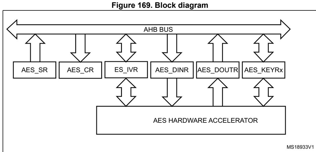
Figure 169. Block diagram
The diagram illustrates the internal architecture of the AES accelerator. At the top, a horizontal double-headed arrow represents the AHB BUS . Below the bus, six rectangular blocks are arranged in a row, each connected to the bus via a vertical double-headed arrow. From left to right, these blocks are labeled: AES_SR , AES_CR , ES_IVR , AES_DINR , AES_DOU TR , and AES_KEYRx . Below this row of blocks is a larger rectangular block labeled AES HARDWARE ACCELERATOR . This central block is connected to the blocks above it via vertical double-headed arrows: specifically, it connects to ES_IVR , AES_DINR , AES_DOU TR , and AES_KEYRx . The AES_SR and AES_CR blocks do not have direct connections to the hardware accelerator. In the bottom right corner of the diagram, the text MS18933V1 is present.
The AES accelerator processes data blocks of 128-bits (4 words) using a key with a length of 128 bits, and an initialization vector when CBC or CTR chaining mode is selected.
It provides 4 operating modes:
- • Mode 1: Encryption using the encryption key stored in the AES_KEYRx registers.
- • Mode 2: Key Derivation stored internally in the AES_KEYRx registers at the end of the key derivation processed from the encryption key stored in this register before enabling the AES. This mode is independent from the AES chaining mode selection.
- • Mode 3: Decryption using a given (pre-computed) decryption key stored in the AES_KEYRx registers.
- • Mode 4: Key Derivation + Decryption using an encryption key stored in the AES_KEYRx registers (not used when the AES is configured in Counter mode for perform a chaining algorithm).
The operating mode is selected by programming bits MODE[1:0] into the AES_CR register. The mode must be changed only when the AES is disabled (bit EN=0 in the AES_CR register). The KEY registers (AES_KEYRx) must be stored before enabling the AES.
To select which one of the ECB, CBC or CTR mode is going to be used for the cryptographic solution, it is mandatory to write the bit CHMOD[1:0] of the AES_CR register and the AES_IVR register (only used for the CBC and CTR chaining modes) when the AES is disabled (bit EN =0 in the AES_CR register).
Once enabled (bit EN=1), the AES is in the input phase, waiting for the software to write the input data words into the AES_DINR (4 words) for the modes 1, 3 or 4. The data corresponds either to the plaintext message or the cipher message. A wait cycle is automatically inserted between two consecutive writes to the AES_DINR register in order to send, interleaved with the data, the key to the AES processor.
For mode 2, the key derivation processing is started immediately after the EN bit in the AES_CR register is set. It requires that the AES_KEYRx registers are loaded with the encrypted KEY before enabling the AES. At the end of the Key derivation processing (CCF flag is set), the derivative key is available in the AES_KEYRx registers and the AES is
disabled by hardware. In this mode, the AES_KEYRx registers must not be read when AES is enabled and until the CCF flag is set to 1 by hardware.
The status flag CCF (Computation Complete Flag) in the AES_SR register is set once the computation phase is complete. An interrupt can be generated if bit CCFIE=1 in the AES_CR register. The software can then read back the data from the AES_DOUTR register (for modes 1, 3, 4) or from the AES_KEYRx registers (if mode 2 is selected).
The flag CCF has no meaning when DMAOUTEN = 1 in the AES_CR register, because the reading the AES_DOUTR register is managed by DMA automatically without any software action at the end of the computation phase.
The operation ends with the output phase, during which the software reads successively the 4 output data words from the AES_DOUTR register in mode 1, 3 or 4. In mode 2 (key derivation mode), the data is automatically stored in the AES_KEYRx registers and the AES is disabled by hardware. Then, software can select mode 3 (decryption mode) before it enables the AES to start the decryption using this derivative key.
During the input and output phases, the software must read or write the data bytes successively (except in mode 2) but the AES is tolerant of any delays occurring between each read or write operation (example: if servicing another interrupt at this time).
The RDERR and WRERR flags in the AES_SR register are set when an unexpected read or write operation is detected. An interrupt can be generated if the ERRRIE bit is set in the AES_CR register. AES is not disabled after an error detection and continues processing as normal.
It is also possible to use the general purpose DMA to write the input words and to read the output words (refer to Figure 184 and Figure 185 ).
The AES can be re-initialized at any moment by resetting the EN bit in the AES_CR register. Then the AES can be re-started from the beginning by setting EN=1, waiting for the first input data byte to be written (except in mode 2 where Key derivation processing starts as soon as the EN bit is set, starting from the value stored in the AES_KEYRx registers).
23.4 Encryption and derivation keys
The AES_KEYRx registers are used to store the encryption or decryption keys. These four registers are organized in little-endian configuration: Register AES_KEYR0 has to be loaded with the 32-bit LSB of the key. Consequently, AES_KEYR3 has to be loaded with the 32-bit MSB of the 128-bit key.
The key for encryption or decryption must be stored in these registers when the AES is disabled (EN = 0 into the AES_CR register). Their endianness are fixed.
In mode 2 (key derivation), the AES_KEYRx needs to be loaded with the encryption key. Then, the AES has to be enabled. At the end of the computation phase, the derivation key is stored automatically in the AES_KEYRx registers, overwriting the previous encryption key. The AES is disabled by hardware when the derivation key is available. If the software needs to switch the AES to mode 3 (decryption mode), there is no need to write the AES_KEYRx registers if their content corresponds to the derivation key (previously computed by mode 2).
In mode 4 (key derivation + decryption), the AES_KEYRx registers contain only the encryption key. The derivation key is calculated internally without any write to these registers.
23.5 AES chaining algorithms
Three algorithms are supported by the AES hardware and can be selected through the CHMOD[1:0] bits in the AES_CR register when the AES is disabled (bit EN = 0):
- • Electronic CodeBook (ECB)
- • Cipher Block Chaining (CBC)
- • Counter Mode (CTR)
23.5.1 Electronic CodeBook (ECB)
This is the default mode. This mode does not use the AES_IVR register. There are no chaining operations. The message is divided into blocks and each block is encrypted separately.
Figure 170 and Figure 171 describe the principle of the Electronic Codebook algorithm for encryption and decryption respectively.
Figure 170. ECB encryption mode
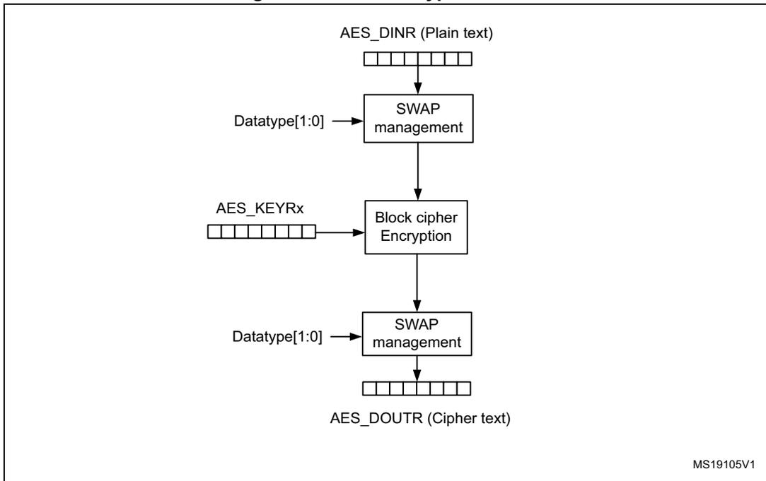
The diagram illustrates the ECB encryption process. It begins with AES_DINR (Plain text) , represented by a horizontal row of five boxes. An arrow points down to a SWAP management block. This block receives an input from the left labeled Datatype[1:0] . An arrow points down from the SWAP management block to a Block cipher Encryption block. This block receives an input from the left labeled AES_KEYRx , which is also represented by a horizontal row of five boxes. An arrow points down from the Block cipher Encryption block to another SWAP management block. This block also receives an input from the left labeled Datatype[1:0] . An arrow points down from this SWAP management block to AES_DOUTR (Cipher text) , represented by a horizontal row of five boxes. The identifier MS19105V1 is located in the bottom right corner of the diagram area.
Figure 171. ECB decryption mode
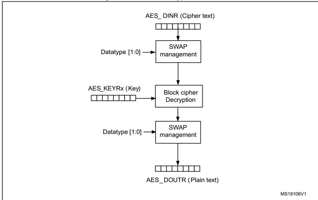
The diagram illustrates the ECB decryption process. It begins with AES_DINR (Cipher text) , represented by a row of five boxes. An arrow points down to a SWAP management block, which receives an input from Datatype [1:0] . From this block, an arrow points down to a Block cipher Decryption block, which receives an input from AES_KEYRx (Key) , also represented by a row of five boxes. From the decryption block, an arrow points down to another SWAP management block, which again receives an input from Datatype [1:0] . Finally, an arrow points down to AES_DOUTR (Plain text) , represented by a row of five boxes. The identifier MS19106V1 is located in the bottom right corner of the diagram area.
23.5.2 Cipher block chaining (CBC)
In cipher-block chaining (CBC) mode, each block of plain text is XORed with the previous cipher text block before being encrypted. To make each message unique, an initialization vector (AES_IVRx) is used during the first block processing.
The initialization vector is XORed after the swapping management block in during encryption mode and before it in decryption mode (refer to Figure 172 and Figure 173 ).
Figure 172. CBC mode encryption
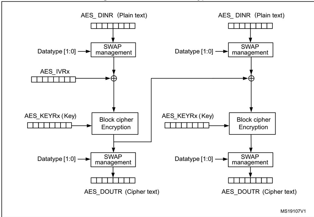
The diagram illustrates the CBC mode encryption process. It consists of two parallel processing paths. In the first path, AES_DINR (Plain text) is input to a SWAP management block. The output of this block is XORed with AES_IVRx . The result is then passed to a Block cipher Encryption block, which also takes AES_KEYRx (Key) as input. The output of the encryption block is processed by another SWAP management block to produce AES_DOUTr (Cipher text) . In the second path, AES_DINR (Plain text) is input to a SWAP management block. The output is XORed with the AES_DOUTr (Cipher text) from the first path. This result is then passed to a Block cipher Encryption block with AES_KEYRx (Key) . The output is processed by a SWAP management block to produce the final AES_DOUTr (Cipher text) . Both paths include Datatype [1:0] control signals for the SWAP management blocks. The identifier MS19107V1 is shown in the bottom right corner.
Figure 173. CBC mode decryption
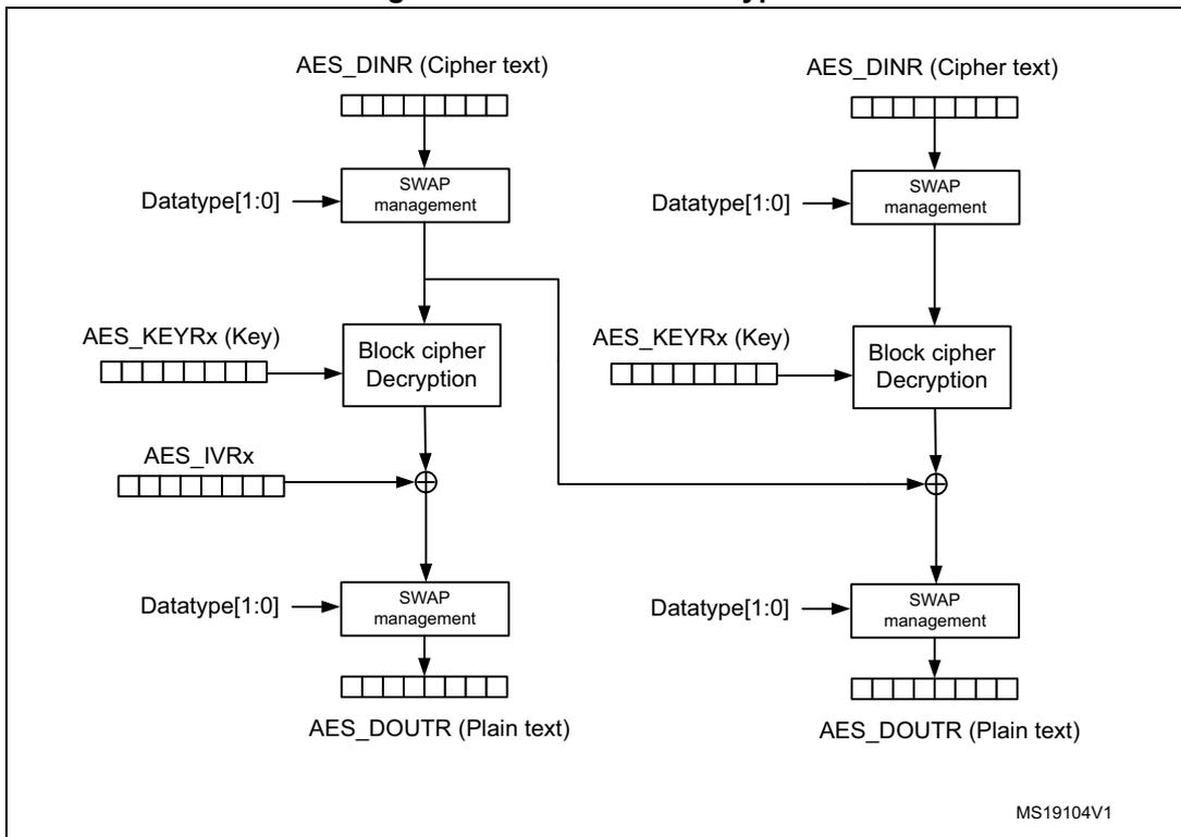
The diagram illustrates the CBC mode decryption process. It consists of two parallel processing paths. In the first path, AES_DINR (Cipher text) is input to a SWAP management block. The output is passed to a Block cipher Decryption block, which also takes AES_KEYRx (Key) as input. The output of the decryption block is XORed with AES_IVRx . The result is then processed by a SWAP management block to produce AES_DOUTr (Plain text) . In the second path, AES_DINR (Cipher text) is input to a SWAP management block. The output is passed to a Block cipher Decryption block with AES_KEYRx (Key) . The output is XORed with the AES_DOUTr (Plain text) from the first path. This result is then processed by a SWAP management block to produce the final AES_DOUTr (Plain text) . Both paths include Datatype[1:0] control signals for the SWAP management blocks. The identifier MS19104V1 is shown in the bottom right corner.
Note: When the AES is enabled, reading the AES_IVR returns the value 0x00000000.
Suspended mode for a given message
It is possible to suspend a message if another message with a higher priority needs to be processed. At the end of sending of this highest priority message, the suspended message may be resumed in both encryption or decryption mode. This feature is available only when the data transfer is done by CPU accesses to the AES_DOUTR and AES_DINR registers. It is advised to not use it when the DMA controller is managing the data transfer.
For correct operation, the message must be suspended at the end of processing a block (after the fourth read of the AES_DOUTR register and before the next AES_DINR write access corresponding to the input of the next block to be processed).
The AES should be disabled writing bit EN = 0 in the AES_CR register. The software has to read the AES_IVRx which contains the latest value to be used for the chaining XOR operation before message interruption. This value has to be stored for reuse by writing the AES_IVRx registers as soon as the interrupted message has to be resumed (when AES is disabled). It should be noted that this does not break the chaining operation and the message processing can be resumed as soon as the AES is enabled again to send the next 128-bit data block.
This behavior is valid whatever the AES configuration (encryption or decryption mode).
Figure 174 gives an example of a message 1 which is suspended in order to send a higher priority message 2, shorter than message 1. At the end of the 128-bit block processing, AES is disabled. The AES_IVR register is read back to store the value to be retrieved later on when the message is resumed, in order not to break the chaining operation. Then, the AES is configured to send message 2 and it is enabled to start processing. At the end of message 2 processing, AES has to be disabled again and the AES_IVRx registers have to be loaded with the value previously stored when the message 1 was interrupted. Then software has to restart from the input value corresponding to block 4 as soon as AES is enabled to resume message 1.
Figure 174. Example of suspend mode management
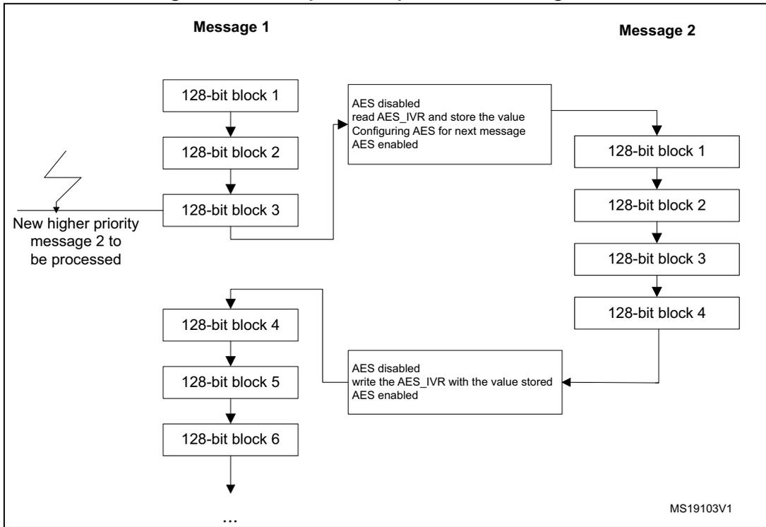
The diagram illustrates the suspend mode management for two messages, Message 1 and Message 2, processed by an AES hardware accelerator. Message 1 consists of 128-bit blocks 1 through 6, followed by more blocks. Message 2 consists of 128-bit blocks 1 through 4. The process starts with Message 1 being processed. After block 3, a new higher priority message (Message 2) arrives. The accelerator suspends Message 1, disabling AES, reading the AES_IVR register, storing its value, configuring AES for the next message, and re-enabling AES. Message 2 is then processed. Upon completion of Message 2, the accelerator disables AES again, writes the stored AES_IVR value back, and re-enables AES to resume Message 1 from block 4.
graph TD; subgraph Message1 [Message 1]; B1_1[128-bit block 1] --> B1_2[128-bit block 2]; B1_2 --> B1_3[128-bit block 3]; B1_3 --> B1_4[128-bit block 4]; B1_4 --> B1_5[128-bit block 5]; B1_5 --> B1_6[128-bit block 6]; B1_6 --> Dots1[...]; end; subgraph Message2 [Message 2]; B2_1[128-bit block 1] --> B2_2[128-bit block 2]; B2_2 --> B2_3[128-bit block 3]; B2_3 --> B2_4[128-bit block 4]; end; B1_3 --> S1[AES disabled<br/>read AES_IVR and store the value<br/>Configuring AES for next message<br/>AES enabled]; S1 --> B2_1; B2_4 --> S2[AES disabled<br/>write the AES_IVR with the value stored<br/>AES enabled]; S2 --> B1_4;
MS19103V1
23.5.3 Counter Mode (CTR)
In counter mode, a 32-bit counter is used in addition to a nonce value for the XOR operation with the cipher text or plain text (refer to Figure 175 and Figure 176 ).
Figure 175. CTR mode encryption
![Figure 175. CTR mode encryption diagram showing two parallel encryption paths. Each path takes a 128-bit key (AES_KEYRx) and a 128-bit IV (AES_IVRx, split into Nonce and counter) as input to a 'Block cipher encryption' block. The output of this block is XORed with the 128-bit plain text (AES_DINR) after it has been processed by a 'Swap management' block (controlled by Datatype[1:0]). The result is then processed by another 'Swap management' block (also controlled by Datatype[1:0]) to produce the 128-bit cipher text (AES_DOUTr). The counter in the IV is incremented for each block.](/RM0038-STM32L100-151-152-162/763047a7d2785d6fc20143c30a01f589_img.jpg)
The diagram illustrates the CTR mode encryption process. It consists of two identical parallel paths. In each path:
- AES_IVRx (128-bit vector) is split into a Nonce (first 96 bits) and a counter (last 32 bits).
- AES_KEYRx (Key) (128-bit vector) and the counter are inputs to the Block cipher encryption block.
- The output of the Block cipher encryption block is XORed ( \( \oplus \) ) with the 128-bit AES_DINR (Plain text) .
- The AES_DINR is first processed by a Swap management block, which is controlled by Datatype[1:0] .
- The XOR result is then processed by another Swap management block, also controlled by Datatype[1:0] , to produce the final AES_DOUTr (Cipher text) .
- The counter from the AES_IVRx is incremented for each block.
MS19102
Figure 176. CTR mode decryption
![Figure 176. CTR mode decryption diagram showing a single decryption path. It takes a 128-bit key (AES_KEYRx) and a 128-bit IV (AES_IVRx, split into Nonce and counter) as input to a 'Block cipher encryption' block. The output of this block is XORed with the 128-bit cipher text (AES_DINR) after it has been processed by a 'Swap management' block (controlled by Datatype[1:0]). The result is then processed by another 'Swap management' block (also controlled by Datatype[1:0]) to produce the 128-bit plain text (AES_DOUTr). The counter in the IV is incremented for each block.](/RM0038-STM32L100-151-152-162/e134abf9e213b2f9dc77221eb512443f_img.jpg)
The diagram illustrates the CTR mode decryption process. It consists of a single path:
- AES_IVRx (128-bit vector) is split into a Nonce (first 96 bits) and a counter (last 32 bits).
- AES_KEYRx (Key) (128-bit vector) and the counter are inputs to the Block cipher encryption block.
- The output of the Block cipher encryption block is XORed ( \( \oplus \) ) with the 128-bit AES_DINR (Cipher text) .
- The AES_DINR is first processed by a Swap management block, which is controlled by Datatype[1:0] .
- The XOR result is then processed by another Swap management block, also controlled by Datatype[1:0] , to produce the final AES_DOUTr (Plain text) .
- The counter from the AES_IVRx is incremented for each block.
MS18942V1
The nonce value and 32-bit counter are accessible through the AES_IVRx register and organized like below in Figure 177 :
Figure 177. 32-bit counter + nonce organization
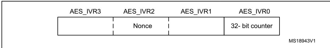
| AES_IVR3 AES_IVR2 AES_IVR1 AES_IVR0 | |||
| Nonce | 32- bit counter | ||
MS18943V1
In Counter Mode, the counter is incremented from the initialized value for each block to be processed in order to guarantee a unique sequence which is not repeated for a long time. It is a 32-bit counter, meaning that the nonce message is kept to the initialized value stored when the AES was disabled. Only the 32-bit LSB of the 128-bit initialization vector register represents the counter. In contrast to CBC mode (which uses the AES_IVRx registers only once when processing the first data block), in Counter mode, the AES_IVRx registers are used for processing each data block.
In counter mode, key derivation+decryption mode is not applicable.
Note: The AES_IVRx register has to be written only when the AES is disabled (bit EN = 0) to guarantee good AES behavior.
Reading it while AES is enabled returns the value 0x00000000.
Reading it while the AES is disabled returns the latest counter value (useful for managing suspend mode).
In CTR mode, key derivation + decryption serves no purpose. Consequently it is forbidden to set MODE[1:0] = 11 in the AES_CR register and any attempt to set this configuration is forced to MODE[1:0] = 10 (which corresponds to CTR mode decryption). This uses the encryption block of the AES processor to decipher the message as shown in Figure 176 .
Suspend mode in CTR mode
Like for the CBC mode, it is possible to interrupt a message, sending a higher priority message and resume the message which was interrupted. Refer to the Figure 174 and Chapter 23.5.2 for more details about the suspend mode capability.
23.6 Data type
Data are entered in the AES processor 32 bits at a time (words), by writing them in the AES_DINR register. AES handles 128-bit data blocks. The AES_DINR or AES_DOUTR registers must be read or written four times to handle one 128-bit data block with the MSB first.
The system memory organization is little-endian: whatever the data type (bit, byte, 16-bit half-word, 32-bit word) used, the less-significant data occupies the lowest address location.
Thus, there must be a bit, byte, or half-word swapping operation to be performed on data to be written in the AES_DINR from system memory before entering the AES processor, and the same swapping must be performed for AES data to be read from the AES_DOUTR register to the system memory, depending on the kind of data to be encrypted or decrypted.
The DATATYPE bits in the AES_CR register offer different swap modes to be applied to the AES_DINR register before sending it to the AES processor and to be applied on the AES_DOUTR register on the data coming out from the processor (refer to Figure 178 ).
Note: The swapping operation concerns only the AES_DOUTR and AES_DINR registers. The AES_KEYRx and AES_IVRx registers are not sensitive to the swap mode selected. They have a fixed little-endian configuration (refer to Section 23.4 and Section 23.12 ).
Figure 178. 128-bit block construction according to the data type
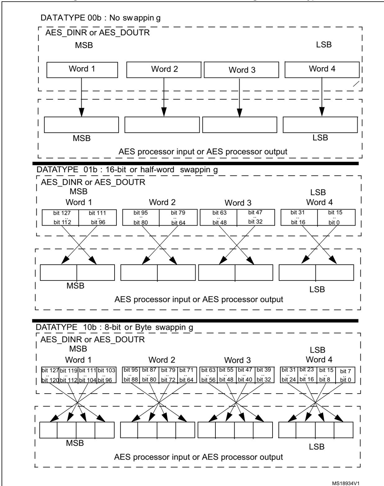
DATATYPE 00b : No swapping
AES_DINR or AES_DOUTR
MSB LSB
Word 1 Word 2 Word 3 Word 4
↓ ↓ ↓ ↓
MSB LSB
AES processor input or AES processor output
DATATYPE 01b : 16-bit or half-word swapping
AES_DINR or AES_DOUTR
MSB LSB
Word 1 Word 2 Word 3 Word 4
| bit 127 bit 112 | bit 111 bit 96 | bit 95 bit 80 | bit 79 bit 64 | bit 63 bit 48 | bit 47 bit 32 | bit 31 bit 16 | bit 15 bit 0 |
↙ ↘ ↙ ↘ ↙ ↘ ↙ ↘
MSB LSB
AES processor input or AES processor output
DATATYPE 10b : 8-bit or Byte swapping
AES_DINR or AES_DOUTR
MSB LSB
Word 1 Word 2 Word 3 Word 4
| bit 127 bit 120 | bit 119 bit 112 | bit 111 bit 104 | bit 103 bit 96 | bit 95 bit 88 | bit 87 bit 80 | bit 79 bit 72 | bit 71 bit 64 | bit 63 bit 56 | bit 55 bit 48 | bit 47 bit 40 | bit 39 bit 32 | bit 31 bit 24 | bit 23 bit 16 | bit 15 bit 8 | bit 7 bit 0 |
↙ ↘ ↘ ↘ ↙ ↘ ↘ ↘ ↙ ↘ ↘ ↘ ↙ ↘ ↘ ↘
MSB LSB
AES processor input or AES processor output
MS18934V1
Figure 179. 128-bit block construction according to the data type (continued)
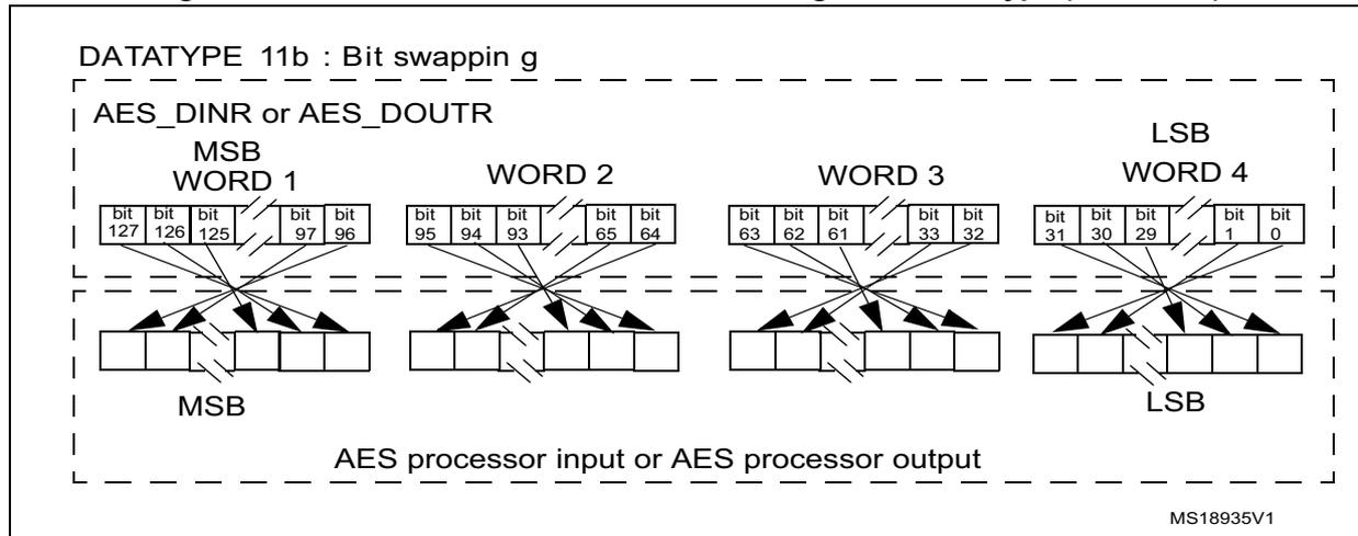
DATATYPE 11b : Bit swapping
AES_DINR or AES_DOUTR
MSB WORD 1 WORD 2 WORD 3 WORD 4 LSB
bit 127 bit 126 bit 125 bit 124 bit 123 bit 122 bit 121 bit 120 bit 119 bit 118 bit 117 bit 116 bit 115 bit 114 bit 113 bit 112 bit 111 bit 110 bit 109 bit 108 bit 107 bit 106 bit 105 bit 104 bit 103 bit 102 bit 101 bit 100 bit 99 bit 98 bit 97 bit 96
bit 95 bit 94 bit 93 bit 92 bit 91 bit 90 bit 89 bit 88 bit 87 bit 86 bit 85 bit 84 bit 83 bit 82 bit 81 bit 80 bit 79 bit 78 bit 77 bit 76 bit 75 bit 74 bit 73 bit 72 bit 71 bit 70 bit 69 bit 68 bit 67 bit 66 bit 65 bit 64
bit 63 bit 62 bit 61 bit 60 bit 59 bit 58 bit 57 bit 56 bit 55 bit 54 bit 53 bit 52 bit 51 bit 50 bit 49 bit 48 bit 47 bit 46 bit 45 bit 44 bit 43 bit 42 bit 41 bit 40 bit 39 bit 38 bit 37 bit 36 bit 35 bit 34 bit 33 bit 32
bit 31 bit 30 bit 29 bit 28 bit 27 bit 26 bit 25 bit 24 bit 23 bit 22 bit 21 bit 20 bit 19 bit 18 bit 17 bit 16 bit 15 bit 14 bit 13 bit 12 bit 11 bit 10 bit 9 bit 8 bit 7 bit 6 bit 5 bit 4 bit 3 bit 2 bit 1 bit 0
MSB LSB
AES processor input or AES processor output
MS18935V1
23.7 Operating modes
23.7.1 Mode 1: encryption
- Disable the AES by resetting the EN bit in the AES_CR register.
- Configure the Mode 1 by programming MODE[1:0]=00 in the AES_CR register and select which type of chaining mode needs to be performed by programming the CHMOD[1:0] bits.
- Write the AES_KEYRx registers (128-bit encryption key) and the AES_IVRx registers if CTR or CBC mode is selected. For EBC mode, the AES_IVRx register is not used.
- Enable the AES by setting the EN bit in the AES_CR register.
- Write the AES_DINR register 4 times to input the plain text (MSB first) as shown in Figure 180: Mode 1: encryption on page 573.
- Wait until the CCF flag is set in the AES_SR register.
- Reads the AES_DOUTR register 4 times to get the cipher text (MSB first) as shown in Figure 180: Mode 1: encryption on page 573.
- Repeat steps 5,6,7 to process all the blocks with the same encryption key.
Figure 180. Mode 1: encryption
![Timing diagram for Mode 1 encryption showing Input phase (4 write operations into AES_DIN[31:0]), Computation phase (Wait until flag CCF = 1), and Output phase (4 read operations of AES_DOUT[31:0]).](/RM0038-STM32L100-151-152-162/19a908bf4693d01556fa4a0d06f25091_img.jpg)
WR PT3 WR PT2 WR PT1 WR PT0
MSB LSB
Wait until flag CCF = 1
RD CT3 RD CT2 RD CT1 RD CT0
MSB LSB
Input phase
4 write operations into
AES_DIN[31:0]
Computation phase
Output phase
4 read operations of
AES_DOUT[31:0]
PT = plaintext = 4 words (PT3, ... , PT0)
CT = ciphertext = 4 words (CT3, ... , CT0)
MS18936V2
23.7.2 Mode 2: key derivation
- 1. Disable the AES by resetting the EN bit in the AES_CR register.
- 2. Configure Mode 2 by programming MODE[1:0]=01 in the AES_CR register. Note that the CHMOD[1:0] bits are not significant in this case because this key derivation mode is independent from the chaining algorithm selected.
- 3. Write the AES_KEYRx registers with the encryption key to obtain the derivative key. A write to the AES_IVRx has no effect.
- 4. Enable the AES by setting the EN bit in the AES_CR register.
- 5. Wait until the CCF flag is set in the AES_SR register.
- 6. The derivation key is put automatically into the AES_KEYRx registers. Read the AES_KEYRx register to obtain the decryption key if needed. The AES is disabled by hardware. To restart a derivation key calculation, repeat steps 3, 4, 5 and 6.
Figure 181. Mode 2: key derivation
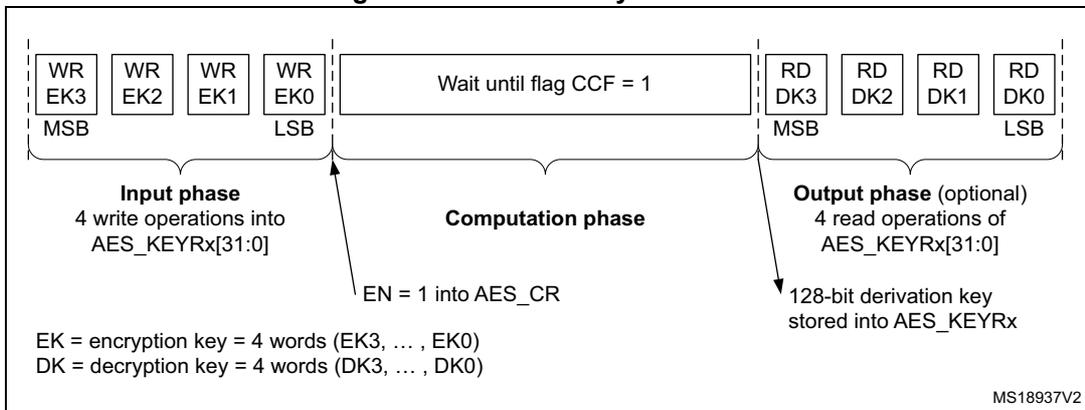
The diagram illustrates the sequence of operations for Mode 2 key derivation. It is divided into three main phases:
- Input phase: Four write operations (WR) into AES_KEYRx[31:0] registers. The registers are labeled EK3, EK2, EK1, and EK0 from MSB to LSB. A bracket below indicates this is the 'Input phase' with '4 write operations into AES_KEYRx[31:0]'. A legend at the bottom left defines EK as encryption key (4 words: EK3, ..., EK0) and DK as decryption key (4 words: DK3, ..., DK0).
- Computation phase: An arrow labeled 'EN = 1 into AES_CR' points into a central block labeled 'Wait until flag CCF = 1'. A bracket below this block is labeled 'Computation phase'.
- Output phase (optional): An arrow points from the 'Wait until flag CCF = 1' block to four read operations (RD) from AES_KEYRx[31:0] registers. The registers are labeled DK3, DK2, DK1, and DK0 from MSB to LSB. A bracket below indicates this is the 'Output phase (optional)' with '4 read operations of AES_KEYRx[31:0]'. A note next to the output phase states '128-bit derivation key stored into AES_KEYRx'.
23.7.3 Mode 3: decryption
- 1. Disable the AES by resetting the EN bit in the AES_CR register.
- 2. Configure Mode 3 by programming MODE[1:0] =10 in the AES_CR register and select which type of chaining mode needs to be performed by programming the CHMOD[1:0] bits.
- 3. Write the AES_KEYRx registers with the decryption key (this step can be bypassed if the derivation key is already stored in the AES_KEYRx registers using mode 2: key derivation). Write the AES_IVRx registers if CTR or CBC mode is selected. For EBC mode, the AES_IVRx registers are not used.
- 4. Enable the AES by setting the EN bit in the AES_CR register.
- 5. Write the AES_DINR register 4 times to input the cipher text (MSB first) as shown in Figure 182: Mode 3: decryption on page 575 .
- 6. Wait until the CCF flag is set in the AES_SR register.
- 7. Read the AES_DOUTR register 4 times to get the plain text (MSB first) as shown in Figure 182: Mode 3: decryption on page 575 .
- 8. Repeat steps 5, 6, 7 to process all the blocks using the same derivation key stored in the AES_KEYRx registers.
Figure 182. Mode 3: decryption
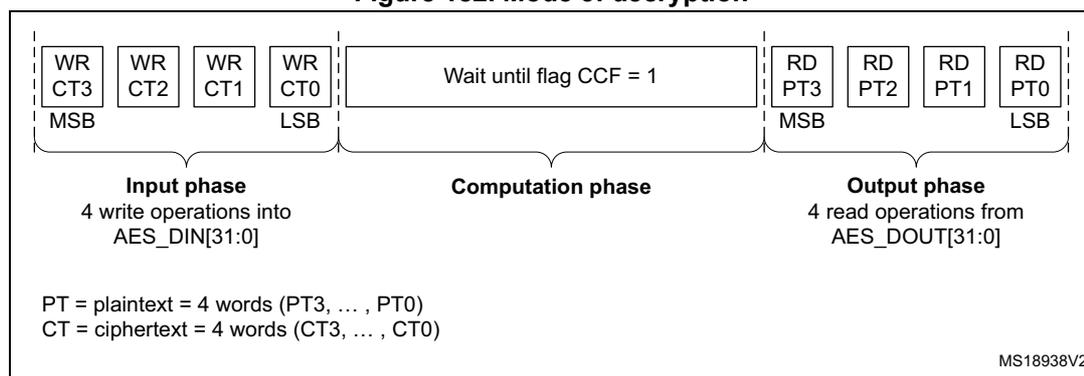
The diagram illustrates the flow of data for Mode 3 decryption. It is divided into three main phases:
- Input phase: Four write operations (WR CT3, WR CT2, WR CT1, WR CT0) are performed into the AES_DIN[31:0] register. The data is ciphertext (CT3, ..., CT0), with CT3 being the Most Significant Byte (MSB) and CT0 the Least Significant Byte (LSB).
- Computation phase: The hardware waits until the CCF flag is set to 1.
- Output phase: Four read operations (RD PT3, RD PT2, RD PT1, RD PT0) are performed from the AES_DOUT[31:0] register. The data is plaintext (PT3, ..., PT0), with PT3 being the MSB and PT0 the LSB.
- PT = plaintext = 4 words (PT3, ..., PT0)
- CT = ciphertext = 4 words (CT3, ..., CT0)
23.7.4 Mode 4: key derivation and decryption
- Disable the AES by resetting the EN bit in the AES_CR register.
- Configure Mode 4 by programming MODE[1:0]=11 in the AES_CR register. This mode is forbidden when AES is configured in CTR mode. It is forced to CTR decryption mode if the software writes MODE[1:0] = 11 and CHMOD[1:0] = 10.
- Write the AES_KEYRx register with the encryption key. Write the AES_IVRx register if the CBC mode is selected.
- Enable the AES by setting the EN bit in the AES_CR register.
- Write the AES_DINR register 4 times to input the cipher text (MSB first) as shown in Figure 183: Mode 4: key derivation and decryption on page 575 .
- Wait until the CCF flag is set in the AES_SR register.
- Read the AES_DOUTR register 4 times to get the plain text (MSB first) as shown in Figure 183: Mode 4: key derivation and decryption on page 575 .
- Repeat steps 5, 6, 7 to process all the blocks with the same encryption key
Note:
The AES_KEYRx registers contain the encryption key during all phases of the processing, No derivation key is stored in these registers. The derivation key starting from the encryption key is stored internally in the AES without storing a copy in the AES_KEYRx registers.
Figure 183. Mode 4: key derivation and decryption
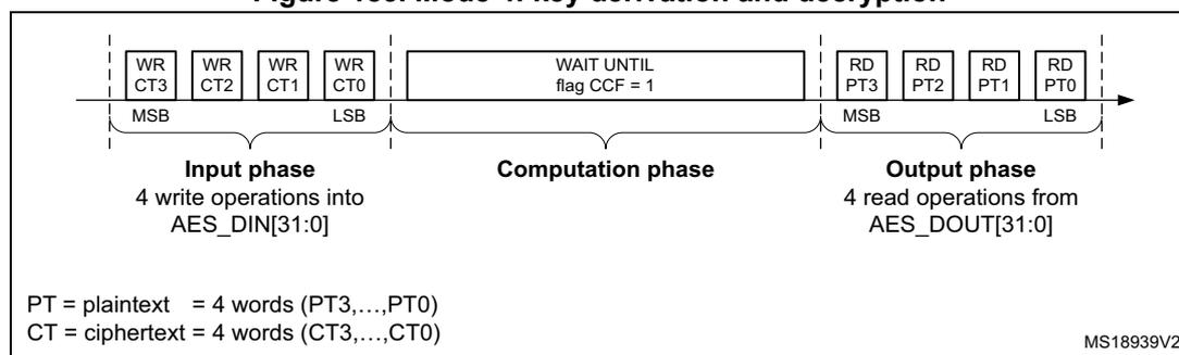
This diagram shows the data flow for Mode 4 decryption, which is identical in structure to Figure 182. It consists of:
- Input phase: Four write operations (WR CT3, WR CT2, WR CT1, WR CT0) into AES_DIN[31:0]. Data is ciphertext (CT3, ..., CT0), MSB to LSB.
- Computation phase: Wait until the CCF flag is set to 1.
- Output phase: Four read operations (RD PT3, RD PT2, RD PT1, RD PT0) from AES_DOUT[31:0]. Data is plaintext (PT3, ..., PT0), MSB to LSB.
- PT = plaintext = 4 words (PT3, ..., PT0)
- CT = ciphertext = 4 words (CT3, ..., CT0)
23.8 AES DMA interface
The AES accelerator provides an interface to connect to the DMA controller.
The DMA must be configured to transfer words.
The AES can be associated with two distinct DMA request channels:
- • A DMA request channel for the inputs: When the DMAINEN bit is set in the AES_CR register, the AES initiates a DMA request (AES_IN) during the INPUT phase each time it requires a word to be written to the AES_DINR register. The DMA channel must be configured in memory-to-peripheral mode with 32-bit data size.
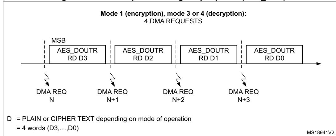
- • A DMA request channel for the outputs: When the DMAOUTEN bit is enabled, the AES initiates a DMA request (AES_OUT) during the OUTPUT phase each time it requires a word to be read from the AES_DOUTR register. The DMA channel must be configured in peripheral-to-memory mode with a data size equal to 32-bit.
Four DMA requests are asserted for each phase, these are described in Figure 184 and Figure 185 .
DMA requests are generated until the AES is disabled. So, after the data output phase at the end of processing a 128-bit data block, the AES switches automatically to a new data input phase for the next data block if any.
Note: For mode 2 (key derivation), access to the AES_KEYRx registers can be done by software using the CPU. No DMA channel is provided for this purpose. Consequently, the DMAINEN bit and DMAOUTEN bits in the AES_CR register have no effect during this mode.
The CCF flag is not relevant when DMAOUTEN = 1 and software does not need to read it in this case. This bit may stay high and has to be cleared by software if the application needs to disable the AES to cancel the DMA management and use CPU access for the data input or data output phase.
Figure 184. DMA requests and data transfers during Input phase (AES_IN)
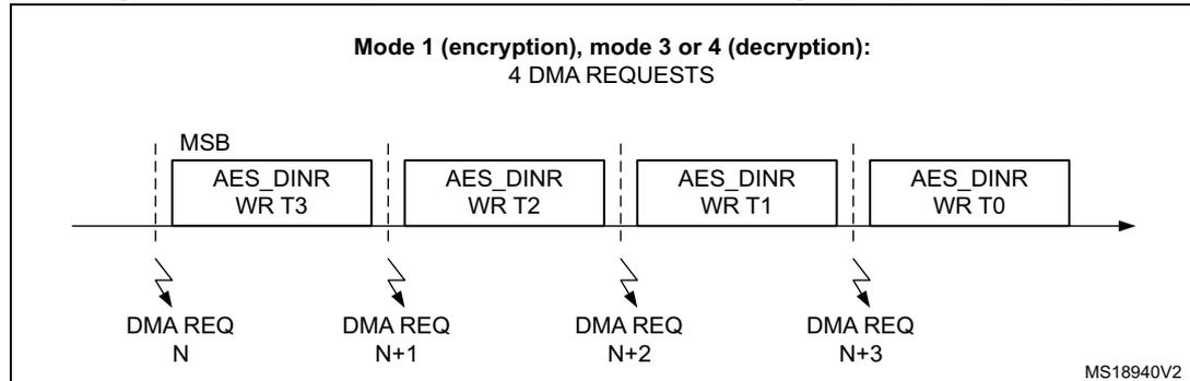
Figure 185. DMA requests during Output phase (AES_OUT)
23.9 Error flags
The RDERR flag in the AES_SR register is set when an unexpected read operation is detected during the computation phase or during the input phase.
The WRERR flag in the AES_SR register is set when an unexpected write operation is detected during the output phase or during the computation phase.
The flags may be cleared setting the respective bit in the AES_CR register (CCFC bit to clear the CCF flag, ERRRC bit to clear the WERR and RDERR flags).
An interrupt can be generated when one of the error flags is set if the ERRRIE bit in the AES_CR register has been previously set.
If an error is detected, AES is not disabled by hardware and continues processing as normal.
23.10 Processing time
The table summarizes the time required to process a 128-bit block for each mode of operation.
Table 96. Processing time (in clock cycle)
| Mode of operation | Input phase | Computation phase | Output phase | Total |
|---|---|---|---|---|
| Mode 1: Encryption | 8 | 202 | 4 | 214 |
| Mode 2: Key derivation | - | 80 | - | 80 |
| Mode 3: Decryption | 8 | 202 | 4 | 214 |
| Mode 4: Key derivation + decryption | 8 | 276 | 4 | 288 |
23.11 AES interrupts
Table 97. AES interrupt requests
| Interrupt event | Event flag | Enable control bit | Exit from Wait |
|---|---|---|---|
| AES computation completed flag | CCF | CCFIE | yes |
| AES read error flag | RDERR | ERRIE | yes |
| AES write error flag | WRERR | ERRIE | yes |
23.12 AES registers
23.12.1 AES control register (AES_CR)
Address offset: 0x00
Reset value: 0x0000 0000
| 31 | 30 | 29 | 28 | 27 | 26 | 25 | 24 | 23 | 22 | 21 | 20 | 19 | 18 | 17 | 16 |
|---|---|---|---|---|---|---|---|---|---|---|---|---|---|---|---|
| Reserved | |||||||||||||||
| r | r | r | r | r | r | r | r | r | r | r | r | r | r | r | r |
| 15 | 14 | 13 | 12 | 11 | 10 | 9 | 8 | 7 | 6 | 5 | 4 | 3 | 2 | 1 | 0 |
| Reserved | DMAO UTEN | DMAI NEN | ERRIE | CCFIE | ERRC | CCFC | CHMOD[1:0] | MODE[1:0] | DATATYPE[1:0] | EN | |||||
| r | r | r | rw | rw | rw | rw | rw | rw | rw | rw | rw | rw | rw | rw | rw |
Bit 31:13 Reserved, read as 0
Bit 12 DMAOUTEN : Enable DMA management of data output phase
- 0: DMA (during data output phase) disabled
- 1: DMA (during data output phase) enabled
If the DMAOUTEN bit is set, DMA requests are generated for the output data phase in mode 1, 3 or 4. This bit has no effect in mode 2 (Key derivation).
Bit 11 DMAINEN : Enable DMA management of data input phase
- 0: DMA (during data input phase) disabled
- 1: DMA (during data input phase) enabled
If the DMAINEN bit is set, DMA requests are generated for the data input phase in mode 1, 3 or 4. This bit has no action in mode 2 (Key Derivation).
Bit 10 ERRIE : Error interrupt enable
An interrupt is generated if at least one of the both flags RDERR or WRERR is set.
- 0: Error interrupt disabled
- 1: Error interrupt enabled
Bit 9 CCFIE : CCF flag interrupt enable
An interrupt is generated if the CCF flag is set.
- 0: CCF interrupt disabled
- 1: CCF interrupt enabled
Bit 8 ERRC : Error clear
Writing 1 to this bit clears the RDERR and WRERR flags.
This bit is always read low.
Bit 7 CCFC : Computation Complete Flag Clear
Writing 1 to this bit clears the CCF flag.
This bit is always read low.
Bits 6:5 CHMOD[1:0] : AES chaining mode
- 00: Electronic codebook (ECB)
- 01: Cipher-Block Chaining (CBC)
- 10: Counter Mode (CTR)
- 11: Reserved.
The AES chaining mode must only be changed while the AES is disabled. Writing these bits while the AES is enabled is forbidden to avoid unpredictable AES behavior.
Bits 4:3 MODE[1:0] : AES operating mode
- 00: Mode 1: Encryption
- 01: Mode 2: Key derivation
- 10: Mode 3: Decryption
- 11: Mode 4: Key derivation + decryption
The operation mode must only be changed if the AES is disabled. Writing these bits while the AES is enabled is forbidden to avoid unpredictable AES behavior.
Mode 4 is forbidden if CTR mode is selected. It is forced to Mode 3 if the software, nevertheless, attempts to set mode 4 for this CTR mode configuration.
Bits 2:1 DATATYPE[1:0] : Data type selection (for data in and data out to/from the cryptographic block)
- 00: 32-bit data. No swapping.
- 01: 16-bit data or half-word. In the word, each half-word is swapped. For example, if one of the four 32-bit data written in the AES_DINR register is 0x764356AB, the value given to the cryptographic block is 0x56AB7643
- 10: 8-bit data or bytes. In the word, all the bytes are swapped. For example, if one of the four 32-bit data written in the AES_DINR register is 0x764356AB, the value given to the cryptographic block is 0xAB564376.
- 11: Bit data. In the word all the bits are swapped. For example, if one of the four 32-bit data written in the AES_DINR register is 0x764356AB, the value given to the cryptographic block is 0xD56AC26E
- The Datatype selection must be changed if the AES is disabled. Writing these bits while the AES is enabled is forbidden to avoid unpredictable AES behavior.
Bits 0 EN : AES enable
- 0: AES disable
- 1: AES enable
The AES can be re-initialized at any moment by resetting this bit: the AES is then ready to start processing a new block when EN is set.
This bit is cleared by hardware when the AES computation is finished in mode 2 (Key derivation)
23.12.2 AES status register (AES_SR)
Address offset: 0x04
Reset value: 0x0000 0000
| 31 | 30 | 29 | 28 | 27 | 26 | 25 | 24 | 23 | 22 | 21 | 20 | 19 | 18 | 17 | 16 |
|---|---|---|---|---|---|---|---|---|---|---|---|---|---|---|---|
| Reserved | |||||||||||||||
| r | r | r | r | r | r | r | r | r | r | r | r | r | r | r | r |
| 15 | 14 | 13 | 12 | 11 | 10 | 9 | 8 | 7 | 6 | 5 | 4 | 3 | 2 | 1 | 0 |
| Reserved | WRERR | RDERR | CCF | ||||||||||||
| r | r | r | r | r | r | r | r | r | r | r | r | r | r | r | r |
Bits 31:3 Reserved, read as 0
Bit 2 WRERR: Write error flag
This bit is set by hardware when an unexpected write operation to the AES_DINR register is detected (during computation or data output phase). An interrupt is generated if the ERRRIE bit has been previously set in the AES_CR register. This flag has no impact on the AES which continues running if even if WERR is set.
It is cleared by software by setting the ERRRC bit in the AES_CR register.
0: No write error detected
1: Write error detected
Bit 1 RDERR: Read error flag
This bit is set by hardware when an unexpected read operation from the AES_DOUTR register is detected (during computation or data input phase). An interrupt is generated if the ERRRIE bit has been previously set in the AES_CR register. This flag has no impact on the AES which continues running if even if RDERR is set.
It is cleared by software by setting the ERRRC bit i in the AES_CR register.
0: No read error detected
1: Read error detected
Bit 0 CCF: Computation complete flag
This bit is set by hardware when the computation is complete. An interrupt is generated if the CCFIE bit has been previously set in the AES_CR register.
It is cleared by software by setting the CCFC bit in the AES_CR register.
0: Computation complete
1: Computation is not complete
Note: This bit is significant only when DMAOUTEN = 0. It may stay high when DMA_EN = 1.
23.12.3 AES data input register (AES_DINR)
Address offset: 0x08
Reset value: 0x0000 0000
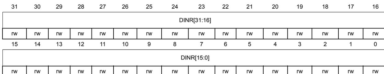
| 31 | 30 | 29 | 28 | 27 | 26 | 25 | 24 | 23 | 22 | 21 | 20 | 19 | 18 | 17 | 16 |
| DINR[31:16] | |||||||||||||||
| rw | rw | rw | rw | rw | rw | rw | rw | rw | rw | rw | rw | rw | rw | rw | rw |
| 15 | 14 | 13 | 12 | 11 | 10 | 9 | 8 | 7 | 6 | 5 | 4 | 3 | 2 | 1 | 0 |
| DINR[15:0] | |||||||||||||||
| rw | rw | rw | rw | rw | rw | rw | rw | rw | rw | rw | rw | rw | rw | rw | rw |
Bits 31:0 DINR[31:0] : Data Input Register.
This register must be written 4 times during the input phase:
- – In Mode 1 (Encryption), 4 words must be written which represent the plain text from MSB to LSB.
- – In Mode 2 (Key Derivation), This register is not used because this mode concerns only derivative key calculation starting from the AES_KEYRx register.
- – In Mode 3 (Decryption) and 4 (Key Derivation+Decryption), 4 words must be written which represent the cipher text MSB to LSB.
Note: This register must be accessed with 32-bit data width.
23.12.4 AES data output register (AES_DOUTR)
Address offset: 0x0C
Reset value: 0x0000 0000
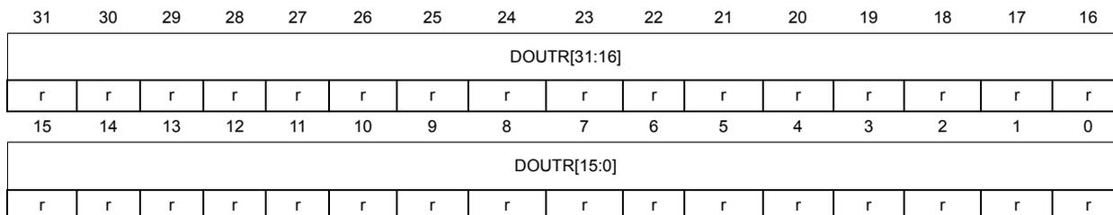
| 31 | 30 | 29 | 28 | 27 | 26 | 25 | 24 | 23 | 22 | 21 | 20 | 19 | 18 | 17 | 16 |
| DOUTR[31:16] | |||||||||||||||
| r | r | r | r | r | r | r | r | r | r | r | r | r | r | r | r |
| 15 | 14 | 13 | 12 | 11 | 10 | 9 | 8 | 7 | 6 | 5 | 4 | 3 | 2 | 1 | 0 |
| DOUTR[15:0] | |||||||||||||||
| r | r | r | r | r | r | r | r | r | r | r | r | r | r | r | r |
Bits 31:0 DOUTR[31:0] : Data output register
This register is read only.
Once the CCF flag (Computation Complete Flag) is set, reading this data register 4 times gives access to the 128-bit output results:
- - In Mode 1 (Encryption), the 4 words read represent the cipher text from MSB to LSB.
- - In Mode 2 (Key Derivation), there is no need to read this register because the derivative key is located in the AES_KEYRx registers.
- - In Mode 3 (Decryption) and Mode 4 (Key Derivation+Decryption), the 4 words read represent the plain text from MSB to LSB.
Note: This register must be accessed with 32-bit data width.
23.12.5 AES key register 0(AES_KEYR0) (LSB: key [31:0])
Address offset: 0x10
Reset value: 0x0000 0000
| 31 | 30 | 29 | 28 | 27 | 26 | 25 | 24 | 23 | 22 | 21 | 20 | 19 | 18 | 17 | 16 |
| KEYR0[31:16] | |||||||||||||||
| rw | rw | rw | rw | rw | rw | rw | rw | rw | rw | rw | rw | rw | rw | rw | rw |
| 15 | 14 | 13 | 12 | 11 | 10 | 9 | 8 | 7 | 6 | 5 | 4 | 3 | 2 | 1 | 0 |
| KEYR0[15:0] | |||||||||||||||
| rw | rw | rw | rw | rw | rw | rw | rw | rw | rw | rw | rw | rw | rw | rw | rw |
Bits 31:0 KEYR0[31:0] : Data Output Register (LSB key [31:0])
This register must be written before the EN bit in the AES_CR register is set:
In Mode 1 (Encryption), mode 2 (Key Derivation) and mode 4 (Key Derivation + Decryption), the value to be written represents the encryption key from LSB, meaning Key [31:0].
In Mode 3 (Decryption), the value to be written represents the decryption key from LSB, meaning Key [31:0]. When the register is written with the encryption key in this decryption mode, reading it before the AES is enabled returns the encryption value. Reading it after CCF flag is set returns the derivation key.
Reading this register while AES is enabled return an unpredictable value.
Note: This register does not contain the derivation key in mode 4 (derivation key + decryption). It always contains the encryption key value.
23.12.6 AES key register 1 (AES_KEYR1) (Key[63:32])
Address offset: 0x14
Reset value: 0x0000 0000
| 31 | 30 | 29 | 28 | 27 | 26 | 25 | 24 | 23 | 22 | 21 | 20 | 19 | 18 | 17 | 16 |
| KEYR1[31:16] | |||||||||||||||
| rw | rw | rw | rw | rw | rw | rw | rw | rw | rw | rw | rw | rw | rw | rw | rw |
| 15 | 14 | 13 | 12 | 11 | 10 | 9 | 8 | 7 | 6 | 5 | 4 | 3 | 2 | 1 | 0 |
| KEYR1[15:0] | |||||||||||||||
| rw | rw | rw | rw | rw | rw | rw | rw | rw | rw | rw | rw | rw | rw | rw | rw |
Bits 31:0 KEYR1[31:0] : AES key register (key [63:32])
Refer to the description of AES_KEYR0.
23.12.7 AES key register 2 (AES_KEYR2) (Key [95:64])
Address offset: 0x18
Reset value: 0x0000 0000

| 31 | 30 | 29 | 28 | 27 | 26 | 25 | 24 | 23 | 22 | 21 | 20 | 19 | 18 | 17 | 16 |
| KEYR2[31:16] | |||||||||||||||
| rw | rw | rw | rw | rw | rw | rw | rw | rw | rw | rw | rw | rw | rw | rw | rw |
| 15 | 14 | 13 | 12 | 11 | 10 | 9 | 8 | 7 | 6 | 5 | 4 | 3 | 2 | 1 | 0 |
| KEYR2[15:0] | |||||||||||||||
| rw | rw | rw | rw | rw | rw | rw | rw | rw | rw | rw | rw | rw | rw | rw | rw |
Bits 31:0
KEYR2[31:0]
: AES key register (key [95:64])
Refer to the description of AES_KEYR0.
23.12.8 AES key register 3 (AES_KEYR3) (MSB: key[127:96])
Address offset: 0x1C
Reset value: 0x0000 0000
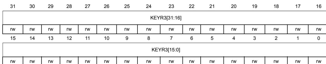
| 31 | 30 | 29 | 28 | 27 | 26 | 25 | 24 | 23 | 22 | 21 | 20 | 19 | 18 | 17 | 16 |
| KEYR3[31:16] | |||||||||||||||
| rw | rw | rw | rw | rw | rw | rw | rw | rw | rw | rw | rw | rw | rw | rw | rw |
| 15 | 14 | 13 | 12 | 11 | 10 | 9 | 8 | 7 | 6 | 5 | 4 | 3 | 2 | 1 | 0 |
| KEYR3[15:0] | |||||||||||||||
| rw | rw | rw | rw | rw | rw | rw | rw | rw | rw | rw | rw | rw | rw | rw | rw |
Bits 31:0
KEYR3[31:0]
: AES key register (MSB key [127:96])
Refer to the description of AES_KEYR0.
23.12.9 AES initialization vector register 0 (AES_IVR0) (LSB: IVR[31:0])
Address offset: 0x20
Reset value: 0x0000 0000
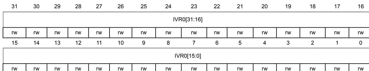
| 31 | 30 | 29 | 28 | 27 | 26 | 25 | 24 | 23 | 22 | 21 | 20 | 19 | 18 | 17 | 16 |
| IVR0[31:16] | |||||||||||||||
| rw | rw | rw | rw | rw | rw | rw | rw | rw | rw | rw | rw | rw | rw | rw | rw |
| 15 | 14 | 13 | 12 | 11 | 10 | 9 | 8 | 7 | 6 | 5 | 4 | 3 | 2 | 1 | 0 |
| IVR0[15:0] | |||||||||||||||
| rw | rw | rw | rw | rw | rw | rw | rw | rw | rw | rw | rw | rw | rw | rw | rw |
Bits 31:0 IVR0[31:0] : initialization vector register (LSB IVR [31:0])
This register must be written before the EN bit in the AES_CR register is set:
The register value has no meaning if:
- - The EBC mode (Electronic codebook) is selected.
- - The CTR or CBC mode is selected in addition with the Key derivation.
- In CTR mode (Counter mode), this register contains the 32-bit counter value.
Reading this register while AES is enabled returns the value 0x00000000.
23.12.10 AES initialization vector register 1 (AES_IVR1) (IVR[63:32])
Address offset: 0x24
Reset value: 0x0000 0000
| 31 | 30 | 29 | 28 | 27 | 26 | 25 | 24 | 23 | 22 | 21 | 20 | 19 | 18 | 17 | 16 |
| IVR1[31:16] | |||||||||||||||
| rw | rw | rw | rw | rw | rw | rw | rw | rw | rw | rw | rw | rw | rw | rw | rw |
| 15 | 14 | 13 | 12 | 11 | 10 | 9 | 8 | 7 | 6 | 5 | 4 | 3 | 2 | 1 | 0 |
| IVR1[15:0] | |||||||||||||||
| rw | rw | rw | rw | rw | rw | rw | rw | rw | rw | rw | rw | rw | rw | rw | rw |
Bits 31:0 IVR1[31:0] : Initialization Vector Register (IVR [63:32])
This register must be written before the EN bit in the AES_CR register is set:
The register value has no meaning if:
- - The EBC mode (Electronic codebook) is selected.
- - The CTR or CBC mode is selected in addition with the Key derivation or key derivation+decryption mode.
- In CTR mode (Counter mode), this register contains the nonce value.
Reading this register while AES is enabled returns the value 0x00000000.
23.12.11 AES initialization vector register 2 (AES_IVR2) (IVR[95:64])
Address offset: 0x28
Reset value: 0x0000 0000
| 31 | 30 | 29 | 28 | 27 | 26 | 25 | 24 | 23 | 22 | 21 | 20 | 19 | 18 | 17 | 16 |
|---|---|---|---|---|---|---|---|---|---|---|---|---|---|---|---|
| IVR2[31:16] | |||||||||||||||
| rw | rw | rw | rw | rw | rw | rw | rw | rw | rw | rw | rw | rw | rw | rw | rw |
| 15 | 14 | 13 | 12 | 11 | 10 | 9 | 8 | 7 | 6 | 5 | 4 | 3 | 2 | 1 | 0 |
| IVR2[15:0] | |||||||||||||||
| rw | rw | rw | rw | rw | rw | rw | rw | rw | rw | rw | rw | rw | rw | rw | rw |
Bits 31:0 IVR2[31:0] : Initialization Vector Register (IVR [95:64])
This register must be written before the EN bit in the AES_CR register is set:
The register value has no meaning if:
- - The EBC mode (Electronic codebook) is selected.
- - The CTR or CBC mode is selected in addition with the Key derivation or key derivation+decryption mode.
In CTR mode (Counter mode), this register contains the nonce value.
Reading this register while AES is enabled returns the value 0x00000000.
23.12.12 AES initialization vector register 3 (AES_IVR3) (MSB: IVR[127:96])
Address offset: 0x2C
Reset value: 0x0000 0000
| 31 | 30 | 29 | 28 | 27 | 26 | 25 | 24 | 23 | 22 | 21 | 20 | 19 | 18 | 17 | 16 |
|---|---|---|---|---|---|---|---|---|---|---|---|---|---|---|---|
| IVR3[31:16] | |||||||||||||||
| rw | rw | rw | rw | rw | rw | rw | rw | rw | rw | rw | rw | rw | rw | rw | rw |
| 15 | 14 | 13 | 12 | 11 | 10 | 9 | 8 | 7 | 6 | 5 | 4 | 3 | 2 | 1 | 0 |
| IVR3[15:0] | |||||||||||||||
| rw | rw | rw | rw | rw | rw | rw | rw | rw | rw | rw | rw | rw | rw | rw | rw |
Bits 31:0 IVR3[31:0] : Initialization Vector Register (MSB IVR [127:96])
This register must be written before the EN bit in the AES_CR register is set:
The register value has no meaning if:
- - The EBC mode (Electronic codebook) is selected.
- - The CTR or CBC mode is selected in addition with the Key derivation or key derivation+decryption mode.
In CTR mode (Counter mode), this register contains the nonce value.
Reading this register while AES is enabled returns the value 0x00000000.
23.12.13 AES register map
The reserved memory areas are highlighted in gray in the table.
Table 98. AES register map
| Offset | Register | 31 | 30 | 29 | 28 | 27 | 26 | 25 | 24 | 23 | 22 | 21 | 20 | 19 | 18 | 17 | 16 | 15 | 14 | 13 | 12 | 11 | 10 | 9 | 8 | 7 | 6 | 5 | 4 | 3 | 2 | 1 | 0 |
|---|---|---|---|---|---|---|---|---|---|---|---|---|---|---|---|---|---|---|---|---|---|---|---|---|---|---|---|---|---|---|---|---|---|
| 0x0000 | AES_CR | Reserved | DMAOUTEN | DMAINEN | ERRIE | CCFIE | ERRC | CCFC | CHMOD[1:0] | MODE[1:0] | DATATYPE[1:0] | EN | |||||||||||||||||||||
| Reset value | 0 | 0 | 0 | 0 | 0 | 0 | 0 | 0 | 0 | 0 | 0 | 0 | 0 | 0 | 0 | 0 | 0 | 0 | 0 | 0 | 0 | 0 | 0 | 0 | 0 | 0 | 0 | 0 | 0 | 0 | 0 | 0 | |
| 0x0004 | AES_SR | Reserved | WRERR | RDERR | CCF | ||||||||||||||||||||||||||||
| Reset value | 0 | 0 | 0 | 0 | 0 | 0 | 0 | 0 | 0 | 0 | 0 | 0 | 0 | 0 | 0 | 0 | 0 | 0 | 0 | 0 | 0 | 0 | 0 | 0 | 0 | 0 | 0 | 0 | 0 | 0 | 0 | ||
| 0x0008 | AES_DINR | AES_DINR[31:0] | |||||||||||||||||||||||||||||||
| Reset value | 0 | 0 | 0 | 0 | 0 | 0 | 0 | 0 | 0 | 0 | 0 | 0 | 0 | 0 | 0 | 0 | 0 | 0 | 0 | 0 | 0 | 0 | 0 | 0 | 0 | 0 | 0 | 0 | 0 | 0 | 0 | ||
| 0x000C | AES_DOUTR | AES_DOUTR[31:0] | |||||||||||||||||||||||||||||||
| Reset value | 0 | 0 | 0 | 0 | 0 | 0 | 0 | 0 | 0 | 0 | 0 | 0 | 0 | 0 | 0 | 0 | 0 | 0 | 0 | 0 | 0 | 0 | 0 | 0 | 0 | 0 | 0 | 0 | 0 | 0 | 0 | ||
| 0x0010 | AES_KEYR0 | AES_KEYR0[31:0] | |||||||||||||||||||||||||||||||
| Reset value | 0 | 0 | 0 | 0 | 0 | 0 | 0 | 0 | 0 | 0 | 0 | 0 | 0 | 0 | 0 | 0 | 0 | 0 | 0 | 0 | 0 | 0 | 0 | 0 | 0 | 0 | 0 | 0 | 0 | 0 | 0 | ||
| 0x0014 | AES_KEYR1 | AES_KEYR1[31:0] | |||||||||||||||||||||||||||||||
| Reset value | 0 | 0 | 0 | 0 | 0 | 0 | 0 | 0 | 0 | 0 | 0 | 0 | 0 | 0 | 0 | 0 | 0 | 0 | 0 | 0 | 0 | 0 | 0 | 0 | 0 | 0 | 0 | 0 | 0 | 0 | 0 | ||
| 0x0018 | AES_KEYR2 | AES_KEYR2[31:0] | |||||||||||||||||||||||||||||||
| Reset value | 0 | 0 | 0 | 0 | 0 | 0 | 0 | 0 | 0 | 0 | 0 | 0 | 0 | 0 | 0 | 0 | 0 | 0 | 0 | 0 | 0 | 0 | 0 | 0 | 0 | 0 | 0 | 0 | 0 | 0 | 0 | ||
| 0x001C | AES_KEYR3 | AES_KEYR3[31:0] | |||||||||||||||||||||||||||||||
| Reset value | 0 | 0 | 0 | 0 | 0 | 0 | 0 | 0 | 0 | 0 | 0 | 0 | 0 | 0 | 0 | 0 | 0 | 0 | 0 | 0 | 0 | 0 | 0 | 0 | 0 | 0 | 0 | 0 | 0 | 0 | 0 | ||
| 0x0020 | AES_IVR0 | AES_IVR0[31:0] | |||||||||||||||||||||||||||||||
| Reset value | 0 | 0 | 0 | 0 | 0 | 0 | 0 | 0 | 0 | 0 | 0 | 0 | 0 | 0 | 0 | 0 | 0 | 0 | 0 | 0 | 0 | 0 | 0 | 0 | 0 | 0 | 0 | 0 | 0 | 0 | 0 | ||
| 0x0024 | AES_IVR1 | AES_IVR1[31:0] | |||||||||||||||||||||||||||||||
| Reset value | 0 | 0 | 0 | 0 | 0 | 0 | 0 | 0 | 0 | 0 | 0 | 0 | 0 | 0 | 0 | 0 | 0 | 0 | 0 | 0 | 0 | 0 | 0 | 0 | 0 | 0 | 0 | 0 | 0 | 0 | 0 | ||
| 0x0028 | AES_IVR2 | AES_IVR2[31:0] | |||||||||||||||||||||||||||||||
| Reset value | 0 | 0 | 0 | 0 | 0 | 0 | 0 | 0 | 0 | 0 | 0 | 0 | 0 | 0 | 0 | 0 | 0 | 0 | 0 | 0 | 0 | 0 | 0 | 0 | 0 | 0 | 0 | 0 | 0 | 0 | 0 | ||
| 0x002C | AES_IVR3 | AES_IVR3[31:0] | |||||||||||||||||||||||||||||||
| Reset value | 0 | 0 | 0 | 0 | 0 | 0 | 0 | 0 | 0 | 0 | 0 | 0 | 0 | 0 | 0 | 0 | 0 | 0 | 0 | 0 | 0 | 0 | 0 | 0 | 0 | 0 | 0 | 0 | 0 | 0 | 0 | ||
Refer to Table 5 on page 47 for the register boundary addresses.