20. Real-time clock (RTC)
20.1 Introduction
The real-time clock (RTC) is an independent BCD timer/counter. The RTC provides a time-of-day clock/calendar, two programmable alarm interrupts, and a periodic programmable wakeup flag with interrupt capability. The RTC also includes an automatic wakeup unit to manage low-power modes.
Two 32-bit registers contain the seconds, minutes, hours (12- or 24-hour format), day (day of week), date (day of month), month, and year, expressed in binary coded decimal format (BCD). The sub-seconds value is also available in binary format (in Cat.2, Cat.3, Cat.4, Cat.5 and Cat.6 devices only).
Compensations for 28-, 29- (leap year), 30-, and 31-day months are performed automatically. Daylight saving time compensation can also be performed.
Additional 32-bit registers contain the programmable alarm subseconds (in Cat.2, Cat.3, Cat.4, Cat.5 and Cat.6 devices only), seconds, minutes, hours, day, and date.
A digital calibration feature is available to compensate for any deviation in crystal oscillator accuracy.
After power-on reset, all RTC registers are protected against possible parasitic write accesses.
As long as the supply voltage remains in the operating range, the RTC never stops, regardless of the device status (Run mode, low-power mode or under reset).
20.2 RTC main features
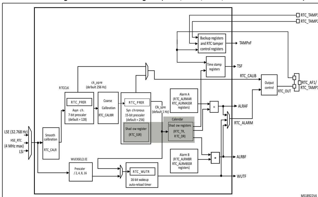
The RTC unit main features are the following (see Figure 164: RTC block diagram (Cat.1 devices) ):
- • Calendar with subseconds(Cat.2, Cat.3, Cat.4, Cat.5 and Cat.6 devices only), seconds, minutes, hours (12 or 24 format), day (day of week), date (day of month), month, and year.
- • Daylight saving compensation programmable by software.
- • Two programmable alarms with interrupt function. The alarms can be triggered by any combination of the calendar fields.
- • Automatic wakeup unit generating a periodic flag that triggers an automatic wakeup interrupt.
- • Reference clock detection: a more precise second source clock (50 or 60 Hz) can be used to enhance the calendar precision.
- • Accurate synchronization with an external clock using the subsecond shift feature (on Cat.2, Cat.3, Cat.4, Cat.5 and Cat.6 devices only).
- • Maskable interrupts/events:
- – Alarm A
- – Alarm B
- – Wakeup interrupt
- – Timestamp
- – Tamper detection
- • Digital calibration circuit (periodic counter correction)
- – 5 ppm accuracy (on Cat.1 devices)
- – 0.95 ppm accuracy (on Cat.2, Cat.3, Cat.4, Cat.5 and Cat.6 devices), obtained in a calibration window of several seconds
- • Timestamp function for event saving (1 event)
- • Tamper detection:
- – 1 tamper event on edge detection (in Cat.1 devices)
- – 3 tamper events with configurable filter and internal pull-up (Cat.2, Cat.3, Cat.4, Cat.5 and Cat.6 devices only).
- – 5 backup registers (20 bytes) in value line, 20 backup registers (80 bytes) in Cat.1 and Cat.2 devices (except value line) and 32 registers (128 bytes) in Cat.3 (except value line), Cat.4, Cat.5 and Cat.6 devices.
- • Alternate function outputs: RTC_OUT which selects one of the following two outputs:
- – RTC_CALIB: 512 Hz or 1 Hz (1 Hz is in Cat.2, Cat.3, Cat.4, Cat.5 and Cat.6 devices only) clock output (with an LSE frequency of 32.768 kHz). This output is
enabled by setting the COE bit in the RTC_CR register. It is routed to the device RTC_AF1 function.
- – RTC_ALARM: Alarm A. This output is selected by configuring the OSEL[1:0] bits in the RTC_CR register. It is routed to the device RTC_AF1 function.
- • RTC alternate function inputs:
- – RTC_TS : timestamp event detection. It is routed to the device RTC_AF1 function.
- – RTC_TAMP1: TAMPER1 event detection. It is routed to the device RTC_AF1 function.
- – RTC_TAMP2: TAMPER2 event detection.
- – RTC_TAMP3: TAMPER3 event detection.
- – RTC_REFIN: reference clock input (usually the mains, 50 or 60 Hz).
Note: Refer to Section 7.4.1: GPIO port mode register (GPIOx_MODER) (x = A..H) for more details on how to select RTC alternate functions (RTC_AF1).
Figure 164. RTC block diagram (Cat.1 devices)
![Figure 164. RTC block diagram (Cat.1 devices). The diagram shows the internal architecture of the RTC. On the left, three clock sources are shown: LSE (32.768 Hz), HSE_RTC (1 MHz max), and LSI. These connect to the RTCCLK input. RTCCLK feeds into an Asynchronous 7-bit prescaler (RTC_PRER, default = 128). The output of this prescaler is ck_apre (default 256 Hz), which goes to a Calibration block. The Calibration block also receives input from the RTC_TS input. The output of the Calibration block is ck_spre (default 1 Hz), which feeds into a Synchronous 13-bit prescaler (RTC_PRER, default = 256). The output of this prescaler is ck, which feeds into the Calendar block. The Calendar block also receives input from the RTC_WUTR (16-bit wakeup auto-reload timer) and the Backup registers and RTC tamper control registers. The Calendar block outputs to two Alarm blocks: Alarm (DTC_ALMAR register) and Alarm (RTC_ALRMBR register). These Alarm blocks output to comparison blocks (=). The output of the DTC_ALMAR comparison block is ALRAF, which feeds into the Output control block. The output of the RTC_ALRMBR comparison block is ALRBF, which also feeds into the Output control block. The Output control block also receives input from the RTC_CALIB (512 Hz) input and the RTC_ALARM input. The Output control block outputs to the RTC_OUT pin, which is connected to the RTC_AF1 function. The RTC_WUTR block also receives input from the Prescaler (WUCKSEL[1:0], / 2, 4, 8, 16) and the Backup registers and RTC tamper control registers. The RTC_WUTR block outputs to the WUTF input. The Backup registers and RTC tamper control registers also receive input from the RTC_TEMP1 input and the TAMPE and TSE inputs. The RTC_TS input also feeds into the Time stamp registers block, which outputs to the Time stamp flag input.](/RM0038-STM32L100-151-152-162/5bbb5f6d3f9396b2f2bcb73f7e83726d_img.jpg)
Figure 165. RTC block diagram (Cat.2, Cat.3, Cat.4, Cat.5 and Cat.6 devices)
20.3 RTC functional description
20.3.1 Clock and prescalers
The RTC clock source (RTCCLK) is selected through the clock controller among the LSE clock, the LSI oscillator clock, and the HSE clock. For more information on the RTC clock source configuration, refer to Section 6: Reset and clock control (RCC) .
A programmable prescaler stage generates a 1 Hz clock which is used to update the calendar. To minimize power consumption, the prescaler is split into 2 programmable prescalers (see Figure 164: RTC block diagram (Cat.1 devices) ):
- • A 7-bit asynchronous prescaler configured through the PREDIV_A bits of the RTC_PRER register.
- • The prescaler features 13 bits for Cat.1 devices, and 15 bits for Cat.2, Cat.3, Cat.4, Cat.5 and Cat.6 devices.
Note: When both prescalers are used, it is recommended to configure the asynchronous prescaler to a high value to minimize consumption.
The asynchronous prescaler division factor is set to 128, and the synchronous division factor to 256, to obtain an internal clock frequency of 1 Hz (ck_spre) with an LSE frequency of 32.768 kHz.
The minimum division factor is 2 in Cat.1 devices and 1 in Cat.2, Cat.3, Cat.4, Cat.5 and Cat.6 devices.
The maximum division factor is \( 2^{20} \) in Cat.1 devices and \( 2^{22} \) in Cat.2, Cat.3, Cat.4, Cat.5 and Cat.6 devices.
This corresponds to a maximum input frequency of around 1 MHz for Cat.1 devices and 4 MHz for Cat.2, Cat.3, Cat.4, Cat.5 and Cat.6 devices.
\( f_{ck\_apre} \) is given by the following formula:
The \( ck\_apre \) clock is used to clock the binary RTC_SSR subseconds downcounter. When it reaches 0, RTC_SSR is reloaded with the content of PREDIV_S. RTC_SSR is available in Cat.2, Cat.3, Cat.4, Cat.5 and Cat.6 devices only.
\( f_{ck\_spre} \) is given by the following formula:
The \( ck\_spre \) clock can be used either to update the calendar or as timebase for the 16-bit wakeup auto-reload timer. To obtain short timeout periods, the 16-bit wakeup auto-reload timer can also run with the RTCCLK divided by the programmable 4-bit asynchronous prescaler (see Section 20.3.4: Periodic auto-wakeup for details).
20.3.2 Real-time clock and calendar
The RTC calendar time and date registers are accessed through shadow registers which are synchronized with PCLK1 (APB1 clock). In Cat.2, Cat.3, Cat.4, Cat.5 and Cat.6 devices, they can also be accessed directly in order to avoid waiting for the synchronization duration.
- • RTC_SSR for the subseconds (available on Cat.2, Cat.3, Cat.4, Cat.5 and Cat.6 devices only)
- • RTC_TR for the time
- • RTC_DR for the date
Every two RTCCLK periods, the current calendar value is copied into the shadow registers, and the RSF bit of RTC_ISR register is set (see Section 20.6.4 ). The copy is not performed in Stop and Standby mode. When exiting these modes, the shadow registers are updated after up to 2 RTCCLK periods.
When the application reads the calendar registers, it accesses the content of the shadow registers. In Cat.2, Cat.3, Cat.4, Cat.5 and Cat.6 devices, it is possible to make a direct access to the calendar registers by setting the BYPSHAD control bit in the RTC_CR register. By default, this bit is cleared, and the user accesses the shadow registers.
When reading the RTC_SSR, RTC_TR or RTC_DR registers in BYPSHAD=0 mode, the frequency of the APB clock ( \( f_{APB} \) ) must be at least 7 times the frequency of the RTC clock ( \( f_{RTCCLK} \) ).
The shadow registers are reset by system reset.
20.3.3 Programmable alarms
The RTC unit provides two programmable alarms, Alarm A and Alarm B.
The programmable alarm functions are enabled through the ALRAIE and ALRBIE bits in the RTC_CR register. The ALRAF and ALRBF flags are set to 1 if the calendar subseconds (Cat.2, Cat.3, Cat.4, Cat.5 and Cat.6 devices only), seconds, minutes, hours, date or day match the values programmed in the alarm registers RTC_ALRMASSR/RTC_ALRMAR and RTC_ALRMBSSR/RTC_ALRMBR, respectively. Each calendar field can be independently selected through the MSKx bits of the RTC_ALRMAR and RTC_ALRMBR registers, and through the MASKSSx bits of the RTC_ALRMASSR and RTC_ALRMBSSR registers. The alarm interrupts are enabled through the ALRAIE and ALRBIE bits in the RTC_CR register.
Alarm A and Alarm B (if enabled by bits OSEL[1:0] in RTC_CR register) can be routed to the RTC_ALARM output. RTC_ALARM polarity can be configured through bit POL in the RTC_CR register.
Caution: If the seconds field is selected (MSK0 bit reset in RTC_ALRMAR or RTC_ALRMBR), the synchronous prescaler division factor set in the RTC_PRER register must be at least 3 to ensure correct behavior.
20.3.4 Periodic auto-wakeup
The periodic wakeup flag is generated by a 16-bit programmable auto-reload down-counter. The wakeup timer range can be extended to 17 bits.
The wakeup function is enabled through the WUTE bit in the RTC_CR register.
The wakeup timer clock input can be:
- • RTC clock (RTCCLK) divided by 2, 4, 8, or 16.
When RTCCLK is LSE(32.768kHz), this allows configuring the wakeup interrupt period from 122 µs to 32 s, with a resolution down to 61µs.
- • ck_spre (usually 1 Hz internal clock)
When ck_spre frequency is 1Hz, this allows achieving a wakeup time from 1 s to around 36 hours with one-second resolution. This large programmable time range is divided in 2 parts:
- – from 1s to 18 hours when WUCKSEL [2:1] = 10
- – and from around 18h to 36h when WUCKSEL[2:1] = 11. In this last case 2 16 is added to the 16-bit counter current value. When the initialization sequence is complete (see Programming the wakeup timer on page 514 ), the timer starts counting down. When the wakeup function is enabled, the down-counting remains active in low-power modes. In addition, when it reaches 0, the WUTF flag is set in the RTC_ISR register, and the wakeup counter is automatically reloaded with its reload value (RTC_WUTR register value).
The WUTF flag must then be cleared by software.
When the periodic wakeup interrupt is enabled by setting the WUTIE bit in the RTC_CR2 register, it can exit the device from low-power modes.
The periodic wakeup flag can be routed to the RTC_ALARM output provided it has been enabled through bits OSEL[1:0] of RTC_CR register. RTC_ALARM polarity can be configured through the POL bit in the RTC_CR register.
System reset, as well as low-power modes (Sleep, Stop and Standby) have no influence on the wakeup timer.
20.3.5 RTC initialization and configuration
RTC register access
The RTC registers are 32-bit registers. The APB interface introduces 2 wait-states in RTC register accesses except on read accesses to calendar shadow registers when BYPSHAD=0.
RTC register write protection
After system reset, the RTC registers are protected against parasitic write access with the DBP bit of the PWR power control register (PWR_CR). The DBP bit must be set to enable RTC registers write access.
After power-on reset, all the RTC registers are write-protected. Writing to the RTC registers is enabled by writing a key into the Write Protection register, RTC_WPR.
The following steps are required to unlock the write protection on all the RTC registers except for RTC_ISR[13:8], RTC_TAFCR, and RTC_BKPxR.
- 1. Write '0xCA' into the RTC_WPR register.
- 2. Write '0x53' into the RTC_WPR register.
Writing a wrong key reactivates the write protection.
The protection mechanism is not affected by system reset.
Calendar initialization and configuration
To program the initial time and date calendar values, including the time format and the prescaler configuration, the following sequence is required:
- 1. Set INIT bit to 1 in the RTC_ISR register to enter initialization mode. In this mode, the calendar counter is stopped and its value can be updated.
- 2. Poll INITF bit of in the RTC_ISR register. The initialization phase mode is entered when INITF is set to 1. It takes from 1 to 2 RTCCLK clock cycles (due to clock synchronization).
- 3. To generate a 1 Hz clock for the calendar counter, program first the synchronous prescaler factor in RTC_PRER register, and then program the asynchronous prescaler factor. Even if only one of the two fields needs to be changed, 2 separate write accesses must be performed to the RTC_PRER register.
- 4. Load the initial time and date values in the shadow registers (RTC_TR and RTC_DR), and configure the time format (12 or 24 hours) through the FMT bit in the RTC_CR register.
- 5. Exit the initialization mode by clearing the INIT bit. The actual calendar counter value is then automatically loaded and the counting restarts after 4 RTCCLK clock cycles.
When the initialization sequence is complete, the calendar starts counting.
Note: After a system reset, the application can read the INITS flag in the RTC_ISR register to check if the calendar has been initialized or not. If this flag equals 0, the calendar has not been initialized since the year field is set at its power-on reset default value (0x00). To read the calendar after initialization, the software must first check that the RSF flag is set in the RTC_ISR register.
Daylight saving time
The daylight saving time management is performed through bits SUB1H, ADD1H, and BKP of the RTC_CR register.
Using SUB1H or ADD1H, the software can subtract or add one hour to the calendar in one single operation without going through the initialization procedure.
In addition, the software can use the BKP bit to memorize this operation.
Programming the alarm
A similar procedure must be followed to program or update the programmable alarms (Alarm A or Alarm B):
- 1. Clear ALRAE or ALRBE in RTC_CR to disable Alarm A or Alarm B.
- 2. Poll ALRAWF or ALRBWF in RTC_ISR until it is set to make sure the access to alarm registers is allowed. In Cat.1 devices, this takes 1 to 2 RTCCLK clock cycles (due to clock synchronization). In Cat.2, Cat.3, Cat.4, Cat.5 and Cat.6 devices, ALRAWF and ALRBWF are always set, so this step can be skipped.
- 3. Program the Alarm A or Alarm B registers (RTC_ALRMASSR/RTC_ALRMAR or RTC_ALRMBSSR/RTC_ALRMBR).
- 4. Set ALRAE or ALRBE in the RTC_CR register to enable Alarm A or Alarm B again.
Note: Each change of the RTC_CR register is taken into account after 1 to 2 RTCCLK clock cycles due to clock synchronization.
Programming the wakeup timer
The following sequence is required to configure or change the wakeup timer auto-reload value (WUT[15:0] in RTC_WUTR):
- 1. Clear WUTE in RTC_CR to disable the wakeup timer.
- 2. Poll WUTWF until it is set in RTC_ISR to make sure the access to wakeup auto-reload counter and to WUCKSEL[2:0] bits is allowed. It takes 1 to 2 RTCCLK clock cycles (due to clock synchronization).
- 3. Program the wakeup auto-reload value WUT[15:0], and the wakeup clock selection (WUCKSEL[2:0] bits in RTC_CR). Set WUTE in RTC_CR to enable the timer again. The wakeup timer restarts down-counting. The WUTWF bit is cleared up to 2 RTCCLK clock cycles after WUTE is cleared, due to clock synchronization.
20.3.6 Reading the calendar
In Cat.1 devices, or when BYPSHAD control bit is cleared in the RTC_CR register
To read the RTC calendar registers (RTC_SSR, RTC_TR and RTC_DR) properly, the APB1 clock frequency ( \( f_{PCLK1} \) ) must be equal to or greater than seven times the \( f_{RTCCLK} \) RTC clock frequency. This ensures a secure behavior of the synchronization mechanism.
If the APB1 clock frequency is less than seven times the RTC clock frequency, the software must read the calendar time and date registers twice. If the second read of the RTC_TR gives the same result as the first read, this ensures that the data is correct. Otherwise a third read access must be done. In any case the APB1 clock frequency must never be lower than the RTC clock frequency.
The RSF bit is set in RTC_ISR register each time the calendar registers are copied into the RTC_SSR, RTC_TR and RTC_DR shadow registers. The copy is performed every two RTCCLK cycles. To ensure consistency between the 3 values, reading either RTC_SSR or RTC_TR locks the values in the higher-order calendar shadow registers until RTC_DR is read. In case the software makes read accesses to the calendar in a time interval smaller than 2 RTCCLK periods: RSF must be cleared by software after the first calendar read, and then the software must wait until RSF is set before reading again the RTC_SSR, RTC_TR and RTC_DR registers.
After waking up from low-power mode (Stop or Standby), RSF must be cleared by software. The software must then wait until it is set again before reading the RTC_SSR, RTC_TR and RTC_DR registers.
The RSF bit must be cleared after wakeup and not before entering low-power mode.
Note: After a system reset, the software must wait until RSF is set before reading the RTC_SSR, RTC_TR and RTC_DR registers. Indeed, a system reset resets the shadow registers to their default values.
After an initialization (refer to Calendar initialization and configuration on page 513 ): the software must wait until RSF is set before reading the RTC_SSR, RTC_TR and RTC_DR registers.
After synchronization (refer to Section 20.3.8: RTC synchronization (Cat.2, Cat.3, Cat.4, Cat.5 and Cat.6 devices only) ): the software must wait until RSF is set before reading the RTC_SSR, RTC_TR and RTC_DR registers.
In Cat.2, Cat.3, Cat.4, Cat.5 and Cat.6 devices, when the BYPSHAD control bit is set in the RTC_CR register (bypass shadow registers)
Reading the calendar registers gives the values from the calendar counters directly, thus eliminating the need to wait for the RSF bit to be set. This is especially useful after exiting from low-power modes (STOP or Standby), since the shadow registers are not updated during these modes.
When the BYPSHAD bit is set to 1, the results of the different registers might not be coherent with each other if an RTCCLK edge occurs between two read accesses to the registers. Additionally, the value of one of the registers may be incorrect if an RTCCLK edge occurs during the read operation. The software must read all the registers twice, and then compare the results to confirm that the data is coherent and correct. Alternatively, the software can just compare the two results of the least-significant calendar register.
Note: While BYPSHAD=1, instructions which read the calendar registers require one extra APB cycle to complete.
20.3.7 Resetting the RTC
The calendar shadow registers (RTC_SSR, RTC_TR and RTC_DR) and some bits of the RTC status register (RTC_ISR) are reset to their default values by all available system reset sources.
On the contrary, the following registers are reset to their default values by a power-on reset and are not affected by a system reset: the RTC current calendar registers, the RTC control register (RTC_CR), the prescaler register (RTC_PRER), the RTC calibration registers (RTC_CALIBR or RTC_CALR), the RTC shift register (RTC_SHIFTR), the RTC timestamp registers (RTC_TSSSR, RTC_TSTR and RTC_TSDR), the RTC tamper and alternate function configuration register (RTC_TAFCR), the RTC backup registers
(RTC_BKPxR), the wakeup timer register (RTC_WUTR), the Alarm A and Alarm B registers (RTC_ALRMASSR/RTC_ALRMAR and RTC_ALRMBSSR/RTC_ALRMBR).
In addition, when the RTC is clocked by the LSE, it goes on running under system reset if the reset source is different from the power-on reset one. Refer to section RTC clock of the Reset and clock controller for details about the list of the RTC clock sources that are not affected by system reset.
When a power-on reset occurs, the RTC is stopped and all the RTC registers are set to their reset values.
20.3.8 RTC synchronization (Cat.2, Cat.3, Cat.4, Cat.5 and Cat.6 devices only)
The RTC can be synchronized to a remote clock with a high degree of precision. After reading the sub-second field (RTC_SSR or RTC_TSSSR), a calculation can be made of the precise offset between the times being maintained by the remote clock and the RTC. The RTC can then be adjusted to eliminate this offset by “shifting” its clock by a fraction of a second using RTC_SHIFTR.
RTC_SSR contains the value of the synchronous prescaler counter. This allows one to calculate the exact time being maintained by the RTC down to a resolution of \( 1 / (PREDIV\_S + 1) \) seconds. As a consequence, the resolution can be improved by increasing the synchronous prescaler value (PREDIV_S[14:0]). The maximum resolution allowed (30.52 µs with a 32768 Hz clock) is obtained with PREDIV_S set to 0x7FFF.
However, increasing PREDIV_S means that PREDIV_A must be decreased in order to maintain the synchronous prescaler output at 1 Hz. In this way, the frequency of the asynchronous prescaler output increases, which may increase the RTC dynamic consumption.
The RTC can be finely adjusted using the RTC shift control register (RTC_SHIFTR). Writing to RTC_SHIFTR can shift (either delay or advance) the clock by up to a second with a resolution of \( 1 / (PREDIV\_S + 1) \) seconds. The shift operation consists of adding the SUBFS[14:0] value to the synchronous prescaler counter SS[15:0]: this delays the clock. If at the same time the ADD1S bit is set, this results in adding one second and at the same time subtracting a fraction of second, so this advances the clock.
Caution: Before initiating a shift operation, the user must check that SS[15] = 0 in order to ensure that no overflow occurs.
As soon as a shift operation is initiated by a write to the RTC_SHIFTR register, the SHPF flag is set by hardware to indicate that a shift operation is pending. This bit is cleared by hardware as soon as the shift operation has completed.
Caution: This synchronization feature is not compatible with the reference clock detection feature: firmware must not write to RTC_SHIFTR when REFCKON=1.
20.3.9 RTC reference clock detection
The RTC calendar update can be synchronized to a reference clock RTC_REFIN, usually the mains (50 or 60 Hz). The RTC_REFIN reference clock should have a higher precision than the 32.768 kHz LSE clock. When the RTC_REFIN detection is enabled (REFCKON bit of RTC_CR set to 1), the calendar is still clocked by the LSE, and RTC_REFIN is used to compensate for the imprecision of the calendar update frequency (1 Hz).
Each 1 Hz clock edge is compared to the nearest reference clock edge (if one is found within a given time window). In most cases, the two clock edges are properly aligned. When the 1 Hz clock becomes misaligned due to the imprecision of the LSE clock, the RTC shifts the 1 Hz clock a bit so that future 1 Hz clock edges are aligned. Thanks to this mechanism, the calendar becomes as precise as the reference clock.
The RTC detects if the reference clock source is present by using the 256 Hz clock (ck_apre) generated from the 32.768 kHz quartz. The detection is performed during a time window around each of the calendar updates (every 1 s). The window equals 7 ck_apre periods when detecting the first reference clock edge. A smaller window of 3 ck_apre periods is used for subsequent calendar updates.
Each time the reference clock is detected in the window, the synchronous prescaler which outputs the ck_spre clock is forced to reload. This has no effect when the reference clock and the 1 Hz clock are aligned because the prescaler is being reloaded at the same moment. When the clocks are not aligned, the reload shifts future 1 Hz clock edges a little for them to be aligned with the reference clock.
If the reference clock halts (no reference clock edge occurred during the 3 ck_apre window), the calendar is updated continuously based solely on the LSE clock. The RTC then waits for the reference clock using a large 7 ck_apre period detection window centered on the ck_spre edge.
When the reference clock detection is enabled, PREDIV_A and PREDIV_S must be set to their default values:
- • PREDIV_A = 0x007F
- • PREDIV_S = 0x00FF
Note: The reference clock detection is not available in Standby mode.
Caution: The reference clock detection feature cannot be used in conjunction with the coarse digital calibration: RTC_CALIBR must be kept at 0x0000 0000 when REFCKON=1.
20.3.10 RTC coarse digital calibration
Two digital calibration methods are available: coarse and smooth calibration. To perform coarse calibration refer to Section 20.6.7: RTC calibration register (RTC_CALIBR) .
Smooth digital calibration is available on Cat.2, Cat.3, Cat.4, Cat.5 and Cat.6 devices only. The two calibration methods are not intended to be used together, the application must select one of the two methods. Coarse calibration is provided for compatibility reasons. To perform smooth calibration refer to Section 20.3.11: RTC smooth digital calibration (Cat.2, Cat.3, Cat.4, Cat.5 and Cat.6 devices only) and the Section 20.6.16: RTC calibration register (RTC_CALR)
The coarse digital calibration can be used to compensate crystal inaccuracy by adding (positive calibration) or masking (negative calibration) clock cycles at the output of the asynchronous prescaler (ck_apre).
Positive and negative calibration are selected by setting the DCS bit in RTC_CALIBR register to '0' and '1', respectively.
When positive calibration is enabled (DCS = '0'), 2 ck_apre cycles are added every minute (around 15360 ck_apre cycles) for 2xDC minutes. This causes the calendar to be updated sooner, thereby adjusting the effective RTC frequency to be a bit higher.
When negative calibration is enabled ( DCS = ‘1’), 1 ck_apre cycle is removed every minute (around 15360 ck_apre cycles) for 2x DC minutes. This causes the calendar to be updated later, thereby adjusting the effective RTC frequency to be a bit lower.
DC is configured through bits DC[4:0] of RTC_CALIBR register. This number ranges from 0 to 31 corresponding to a time interval (2x DC ) ranging from 0 to 62.
The coarse digital calibration can be configured only in initialization mode, and starts when the INIT bit is cleared. The full calibration cycle lasts 64 minutes. The first 2x DC minutes of the 64 -minute cycle are modified as just described.
Negative calibration can be performed with a resolution of about 2 ppm while positive calibration can be performed with a resolution of about 4 ppm. The maximum calibration ranges from -63 ppm to 126 ppm.
The calibration can be performed either on the LSE or on the HSE clock.
Caution: Digital calibration may not work correctly if PREDIV_A < 6.
Case of RTCCLK=32.768 kHz and PREDIV_A+1=128
The following description assumes that ck_apre frequency is 256 Hz obtained with an LSE clock nominal frequency of 32.768 kHz, and PREDIV_A set to 127 (default value).
The ck_spre clock frequency is only modified during the first 2x DC minutes of the 64-minute cycle. For example, when DC equals 1, only the first 2 minutes are modified. This means that the first 2x DC minutes of each 64-minute cycle have, once per minute, one second either shortened by 256 or lengthened by 128 RTCCLK cycles, given that each ck_apre cycle represents 128 RTCCLK cycles (with PREDIV_A +1=128).
Therefore each calibration step has the effect of adding 512 or subtracting 256 oscillator cycles for every 125829120 RTCCLK cycles (64min x 60 s/min x 32768 cycles/s). This is equivalent to +4.069 ppm or -2.035 ppm per calibration step. As a result, the calibration resolution is +10.5 or -5.27 seconds per month, and the total calibration ranges from +5.45 to -2.72 minutes per month.
In order to measure the clock deviation, a 512 Hz clock is output for calibration. Refer to Section 20.3.14: Calibration clock output .
20.3.11 RTC smooth digital calibration (Cat.2, Cat.3, Cat.4, Cat.5 and Cat.6 devices only)
In Cat.2, Cat.3, Cat.4, Cat.5 and Cat.6 devices, the RTC frequency can be digitally calibrated with a resolution of about 0.954 ppm with a range from -487.1 ppm to +488.5 ppm. The correction of the frequency is performed using series of small adjustments (adding and/or subtracting individual RTCCLK pulses). These adjustments are fairly well distributed so that the RTC is well calibrated even when observed over short durations of time.
The smooth digital calibration is performed during a cycle of about \( 2^{20} \) RTCCLK pulses, or 32 seconds when the input frequency is 32768 Hz. This cycle is maintained by a 20-bit counter, cal_cnt[19:0], clocked by RTCCLK.
The smooth calibration register (RTC_CALR) specifies the number of RTCCLK clock cycles to be masked during the 32-second cycle:
- • Setting the bit CALM[0] to 1 causes exactly one pulse to be masked during the 32-second cycle.
- • Setting CALM[1] to 1 causes two additional cycles to be masked
- • Setting CALM[2] to 1 causes four additional cycles to be masked
- • and so on up to CALM[8] set to 1 which causes 256 clocks to be masked.
Note: CALM[8:0] (RTC_CALRx) specifies the number of RTCCLK pulses to be masked during the 32-second cycle. Setting the bit CALM[0] to '1' causes exactly one pulse to be masked during the 32-second cycle at the moment when cal_cnt[19:0] is 0x80000 ; CALM[1]=1 causes two other cycles to be masked (when cal_cnt is 0x40000 and 0xC0000) ; CALM[2]=1 causes four other cycles to be masked (cal_cnt = 0x20000/0x60000/0xA0000/ 0xE0000) ; and so on up to CALM[8]=1 which causes 256 clocks to be masked (cal_cnt = 0xXX800) .
While CALM allows the RTC frequency to be reduced by up to 487.1 ppm with fine resolution, the bit CALP can be used to increase the frequency by 488.5 ppm. Setting CALP to '1' effectively inserts an extra RTCCLK pulse every \( 2^{11} \) RTCCLK cycles, which means that 512 clocks are added during every 32-second cycle.
Using CALM together with CALP, an offset ranging from -511 to +512 RTCCLK cycles can be added during the 32-second cycle, which translates to a calibration range of -487.1 ppm to +488.5 ppm with a resolution of about 0.954 ppm.
The formula to calculate the effective calibrated frequency (FCAL) given the input frequency (FRTCCLK) is as follows:
Calibration when PREDIV_A<3
The CALP bit can not be set to 1 when the asynchronous prescaler value (PREDIV_A bits in RTC_PRER register) is less than 3. If CALP was already set to 1 and PREDIV_A bits are set to a value less than 3, CALP is ignored and the calibration operates as if CALP was equal to 0.
To perform a calibration with PREDIV_A less than 3, the synchronous prescaler value (PREDIV_S) should be reduced so that each second is accelerated by 8 RTCCLK clock cycles, which is equivalent to adding 256 clock cycles every 32 seconds. As a result, between 255 and 256 clock pulses (corresponding to a calibration range from 243.3 to 244.1 ppm) can effectively be added during each 32-second cycle using only the CALM bits.
With a nominal RTCCLK frequency of 32768 Hz, when PREDIV_A equals 1 (division factor of 2), PREDIV_S should be set to 16379 rather than 16383 (4 less). The only other interesting case is when PREDIV_A equals 0, PREDIV_S should be set to 32759 rather than 32767 (8 less).
If PREDIV_S is reduced in this way, the formula given the effective frequency of the calibrated input clock is as follows:
In this case, CALM[7:0] equals 0x100 (the midpoint of the CALM range) is the correct setting if RTCCLK is exactly 32768.00 Hz.
Verifying the RTC calibration
RTC precision is performed by measuring the precise frequency of RTCCLK and calculating the correct CALM value and CALP values. An optional 1 Hz output is provided on Cat.2, Cat.3, Cat.4, Cat.5 and Cat.6 devices to allow applications to measure and verify the RTC precision.
Measuring the precise frequency of the RTC over a limited interval can result in a measurement error of up to 2 RTCCLK clock cycles over the measurement period, depending on how the digital calibration cycle is aligned with the measurement period.
However, this measurement error can be eliminated if the measurement period is the same length as the calibration cycle period. In this case, the only error observed is the error due to the resolution of the digital calibration.
- • By default, the calibration cycle period is 32 seconds.
Using this mode and measuring the accuracy of the 1 Hz output over exactly 32 seconds guarantees that the measure is within 0.477 ppm (0.5 RTCCLK cycles over 32 seconds, due to the limitation of the calibration resolution). - • CALW16 bit of the RTC_CALR register can be set to 1 to force a 16- second calibration cycle period.
In this case, the RTC precision can be measured during 16 seconds with a maximum error of 0.954 ppm (0.5 RTCCLK cycles over 16 seconds). However, since the calibration resolution is reduced, the long term RTC precision is also reduced to 0.954 ppm: CALM[0] bit is stuck at 0 when CALW16 is set to 1. - • CALW8 bit of the RTC_CALR register can be set to 1 to force a 8- second calibration cycle period.
In this case, the RTC precision can be measured during 8 seconds with a maximum error of 1.907 ppm (0.5 RTCCLK cycles over 8s). The long term RTC precision is also reduced to 1.907 ppm: CALM[1:0] bits are stuck at 00 when CALW8 is set to 1.
Re-calibration on-the-fly
The calibration register (RTC_CALR) can be updated on-the-fly while RTC_ISR/INITF=0, by using the follow process:
- 1. Poll the RTC_ISR/RECALPF (re-calibration pending flag).
- 2. If it is set to 0, write a new value to RTC_CALR, if necessary. RECALPF is then automatically set to 1
- 3. Within three ck_apre cycles after the write operation to RTC_CALR, the new calibration settings take effect.
20.3.12 Timestamp function
Timestamp is enabled by setting the TSE bit of RTC_CR register to 1.
The calendar is saved in the timestamp registers (RTC_TSSSR, RTC_TSTR, RTC_TSDR) when a timestamp event is detected on the pin to which the TIMESTAMP alternate function is mapped. When a timestamp event occurs, the timestamp flag bit (TSF) in RTC_ISR register is set.
By setting the TSIE bit in the RTC_CR register, an interrupt is generated when a timestamp event occurs.
If a new timestamp event is detected while the timestamp flag (TSF) is already set, the timestamp overflow flag (TSOVF) flag is set and the timestamp registers (RTC_TSTR and RTC_TSDR) maintain the results of the previous event.
Note: TSF is set 2 ck_apre cycles after the timestamp event occurs due to synchronization process.
There is no delay in the setting of TSOVF. This means that if two timestamp events are close together, TSOVF can be seen as '1' while TSF is still '0'. As a consequence, it is recommended to poll TSOVF only after TSF has been set.
Caution: If a timestamp event occurs immediately after the TSF bit is supposed to be cleared, then both TSF and TSOVF bits are set. To avoid masking a timestamp event occurring at the same moment, the application must not write '0' into TSF bit unless it has already read it to '1'.
Optionally, a tamper event can cause a timestamp to be recorded. See the description of the TAMPTS control bit in Section 20.6.17: RTC tamper and alternate function configuration register (RTC_TAFCR) . If the timestamp event is on the same pin as a tamper event configured in filtered mode (TAMPFLT set to a non-zero value), the timestamp on tamper detection event mode must be selected by setting TAMPTS='1' in RTC_TAFCR register.
TIMESTAMP alternate function
The TIMESTAMP alternate function (RTC_TS) is mapped to RTC_AF1.
20.3.13 Tamper detection
One tamper detection input on edge detection is available on Cat.1 devices.
Three tamper detection inputs are available on Cat.2, Cat.3, Cat.4, Cat.5 and Cat.6 devices. They can be configured either for edge detection, or for level detection with filtering.
RTC backup registers
The backup registers (RTC_BKPxR) are five 32-bit registers in value line devices for storing 20 bytes of user application data, twenty 32-bit registers in Cat.1 and Cat.2 devices (except value line) for storing 80 bytes of user application data and thirty-two 32-bit registers in Cat.3 (except value line), Cat.4, Cat.5 and Cat.6 devices for storing 128 bytes of user application data. They are implemented in the V DD domain. They are not reset by system reset or when the device wakes up from Standby mode. They are reset by a power-on reset.
The backup registers are reset when a tamper detection event occurs (see Section 20.6.20: RTC backup registers (RTC_BKPxR) and Tamper detection initialization on page 521 ).
Tamper detection initialization
Each tamper detection input is associated with the TAMP1F/TAMP2F/ TAMP3F flags in the RTC_ISR2 register. Each input can be enabled by setting the corresponding TAMP1E/TAMP2E/TAMP3E bits to 1 in the RTC_TAFCR register.
A tamper detection event resets all backup registers (RTC_BKPxR).
By setting the TAMPIE bit in the RTC_TAFCR register, an interrupt is generated when a tamper detection event occurs.
Timestamp on tamper event
With TAMPTS set to '1 (high devices only)', any tamper event causes a timestamp to occur. In this case, either the TSF bit or the TSOVF bit are set in RTC_ISR, in the same manner as if a normal timestamp event occurs. The affected tamper flag register (TAMP1F, TAMP2F, or TAMP3F) is set at the same time that TSF or TSOVF is set.
Edge detection on tamper inputs
If the TAMPFLT bits are "00", the TAMPER pins generate tamper detection events (RTC_TAMP[3:1]) when either a rising edge is observed or a falling edge is observed depending on the corresponding TAMPxTRG bit. The internal pull-up resistors on the TAMPER input are deactivated when edge detection is selected.
Caution: To avoid losing tamper detection events, the signal used for edge detection is logically ANDed with TAMPxE in order to detect a tamper detection event in case it occurs before the TAMPERx pin is enabled.
- • When TAMPxTRG = 0: if the TAMPERx alternate function is already high before tamper detection is enabled (TAMPxE bit set to 1), a tamper event is detected as soon as TAMPERx is enabled, even if there was no rising edge on TAMPERx after TAMPxE was set.
- • When TAMPxTRG = 1: if the TAMPERx alternate function is already low before tamper detection is enabled, a tamper event is detected as soon as TAMPERx is enabled (even if there was no falling edge on TAMPERx after TAMPxE was set).
After a tamper event has been detected and cleared, the TAMPERx alternate function should be disabled and then re-enabled (TAMPxE set to 1) before re-programming the backup registers (RTC_BKPxR). This prevents the application from writing to the backup registers while the TAMPERx value still indicates a tamper detection. This is equivalent to a level detection on the TAMPERx alternate function.
Note: Tamper detection is still active when V DD power is switched off. To avoid unwanted resetting of the backup registers, the pin to which the TAMPER alternate function is mapped should be externally tied to the correct level.
Level detection with filtering on tamper inputs (Cat.2, Cat.3, Cat.4, Cat.5 and Cat.6 devices only)
Level detection with filtering is performed by setting TAMPFLT to a non-zero value. A tamper detection event is generated when either 2, 4, or 8 (depending on TAMPFLT) consecutive samples are observed at the level designated by the TAMPxTRG bits (TAMP1TRG/TAMP2TRG/TAMP3TRG).
The TAMPER inputs are pre-charged through the I/O internal pull-up resistance before its state is sampled, unless disabled by setting TAMPPUDIS to 1. The duration of the precharge is determined by the TAMPPRCH bits, allowing for larger capacitances on the tamper inputs.
The trade-off between tamper detection latency and power consumption through the pull-up can be optimized by using TAMPFREQ to determine the frequency of the sampling for level detection.
Note: Refer to the datasheets for the electrical characteristics of the pull-up resistors.
TAMPER alternate function detection
The TAMPER1 alternate function (RTC_TAMP1) is mapped to RTC_AF1. The TAMPER 2 and TAMPER 3 alternate functions are RTC_TAMP2 and RTC_TAMP3 respectively.
20.3.14 Calibration clock output
When the COE bit is set to 1 in the RTC_CR register, a reference clock is provided on the RTC_CALIB device output. If the COSEL bit in the RTC_CR register is reset and PREDIV_A = 0x7F, the RTC_CALIB frequency is \( f_{RTCCLK}/64 \) . This corresponds to a calibration output at 512 Hz for an RTCCLK frequency at 32.768 kHz.
The RTC_CALIB output is not impacted by the calibration value programmed in RTC_CALIBR register. The RTC_CALIB duty cycle is irregular: there is a light jitter on falling edges. It is therefore recommended to use rising edges.
If COSEL is set (on Cat.2, Cat.3, Cat.4, Cat.5 and Cat.6 devices) and (PREDIV_S+1) is a non-zero multiple of 256 (i.e: PREDIV_S[7:0] = 0xFF), the RTC_CALIB frequency is \( f_{RTCCLK}/(256 * (PREDIV_A+1)) \) . This corresponds to a calibration output at 1 Hz for prescaler default values (PREDIV_A = 0x7F, PREDIV_S = 0xFF), with an RTCCLK frequency at 32.768 kHz. The 1 Hz output is affected when a shift operation is on going and may toggle during the shift operation (SHPF=1).
Calibration alternate function output
When the COE bit in the RTC_CR register is set to 1, the calibration alternate function (RTC_CALIB) is enabled on RTC_AF1.
Note: When RTC_CALIB or RTC_ALARM is selected, RTC_AF1 is automatically configured in output alternate function.
20.3.15 Alarm output
Three functions can be selected on Alarm output: ALRAF, ALRBF and WUTF. These functions reflect the contents of the corresponding flags in the RTC_ISR register.
The OSEL[1:0] control bits in the RTC_CR register are used to activate the alarm alternate function output (RTC_ALARM) in RTC_AF1, and to select the function which is output on RTC_ALARM.
The polarity of the output is determined by the POL control bit in RTC_CR so that the opposite of the selected flag bit is output when POL is set to 1.
Alarm alternate function output
RTC_ALARM can be configured in output open drain or output push-pull using the control bit ALARMOUTTYPE in the RTC_TAFCR register.
Note: The RTC_CALIB should be disabled (COE bit must be kept cleared).
When RTC_CALIB or RTC_ALARM is selected, RTC_AF1 is automatically configured in output alternate function.
20.4 RTC and low-power modes
Table 89. Effect of low-power modes on RTC
| Mode | Description |
|---|---|
| Sleep | No effect RTC interrupts cause the device to exit the Sleep mode. |
| Stop | The RTC remains active when the RTC clock source is LSE or LSI. RTC alarm, RTC tamper event, RTC time stamp event, and RTC Wakeup cause the device to exit the Stop mode. |
| Standby | The RTC remains active when the RTC clock source is LSE or LSI. RTC alarm, RTC tamper event, RTC time stamp event, and RTC Wakeup cause the device to exit the Standby mode. |
20.5 RTC interrupts
All RTC interrupts are connected to the EXTI controller.
To enable the RTC Alarm interrupt, the following sequence is required:
- 1. Configure and enable the EXTI Line 17 in interrupt mode and select the rising edge sensitivity.
- 2. Configure and enable the RTC_Alarm IRQ channel in the NVIC.
- 3. Configure the RTC to generate RTC alarms (Alarm A or Alarm B).
To enable the RTC Wakeup interrupt, the following sequence is required:
- 1. Configure and enable the EXTI Line 20 in interrupt mode and select the rising edge sensitivity.
- 2. Configure and enable the RTC_WKUP IRQ channel in the NVIC.
- 3. Configure the RTC to generate the RTC wakeup timer event.
To enable the RTC Tamper interrupt, the following sequence is required:
- 1. Configure and enable the EXTI Line 19 in interrupt mode and select the rising edge sensitivity.
- 2. Configure and Enable the TAMP_STAMP IRQ channel in the NVIC.
- 3. Configure the RTC to detect the RTC tamper event.
To enable the RTC TimeStamp interrupt, the following sequence is required:
- 1. Configure and enable the EXTI Line 19 in interrupt mode and select the rising edge sensitivity.
- 2. Configure and Enable the TAMP_STAMP IRQ channel in the NVIC.
- 3. Configure the RTC to detect the RTC timestamp event.
Table 90. Interrupt control bits
| Interrupt event | Event flag | Enable control bit | Exit the Sleep mode | Exit the Stop mode | Exit the Standby mode |
|---|---|---|---|---|---|
| Alarm A | ALRAF | ALRAIE | yes | yes (1) | yes (1) |
| Alarm B | ALRBF | ALRBIE | yes | yes (1) | yes (1) |
| Wakeup | WUTF | WUTIE | yes | yes (1) | yes (1) |
| TimeStamp | TSF | TSIE | yes | yes (1) | yes (1) |
| Tamper1 detection | TAMP1F | TAMPIE | yes | yes (1) | yes (1) |
| Tamper2 detection (2) | TAMP2F | TAMPIE | yes | yes (1) | yes (1) |
| Tamper3 detection (3) | TAMP3F | TAMPIE | yes | yes (1) | yes (1) |
- 1. Wakeup from STOP and Standby modes is possible only when the RTC clock source is LSE or LSI.
- 2. If RTC_TAMPER2 pin is present (only on Cat.2, Cat.3, Cat.4, Cat.5 and Cat.6 devices). Refer to device datasheet pinout.
- 3. Only on Cat.2, Cat.3, Cat.4, Cat.5 and Cat.6 devices if RTC_TAMPER3 pin is present. Refer to device datasheet pinout.
20.6 RTC registers
Refer to Section 1.1: List of abbreviations for registers for a list of abbreviations used in register descriptions.
The peripheral registers have to be accessed by words (32 bits).
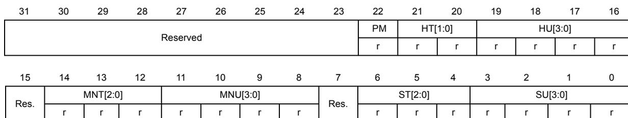
20.6.1 RTC time register (RTC_TR)
The RTC_TR is the calendar time shadow register. This register must be written in initialization mode only. Refer to Calendar initialization and configuration on page 513 and Reading the calendar on page 514 .
Address offset: 0x00
Power-on reset value: 0x0000 0000
System reset: 0x0000 0000 when BYPSHAD = 0. Not affected when BYPSHAD = 1.
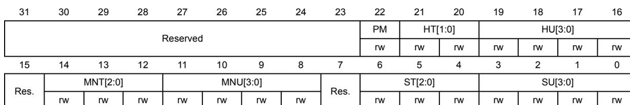
| 31 | 30 | 29 | 28 | 27 | 26 | 25 | 24 | 23 | 22 | 21 | 20 | 19 | 18 | 17 | 16 |
| Reserved | PM | HT[1:0] | HU[3:0] | ||||||||||||
| rw | rw | rw | rw | rw | rw | rw | |||||||||
| 15 | 14 | 13 | 12 | 11 | 10 | 9 | 8 | 7 | 6 | 5 | 4 | 3 | 2 | 1 | 0 |
| Res. | MNT[2:0] | MNU[3:0] | Res. | ST[2:0] | SU[3:0] | ||||||||||
| rw | rw | rw | rw | rw | rw | rw | rw | rw | rw | rw | rw | rw | rw | ||
Bits 31-24 Reserved
Bit 23 Reserved, must be kept at reset value.
Bit 22
PM
: AM/PM notation
0: AM or 24-hour format
1: PM
Bits 21-20 HT[1:0] : Hour tens in BCD format
Bits 19-16 HU[3:0] : Hour units in BCD format
Bit 15 Reserved, must be kept at reset value.
Bits 14-12 MNT[2:0] : Minute tens in BCD format
Bits 11-8 MNU[3:0] : Minute units in BCD format
Bit 7 Reserved, must be kept at reset value.
Bits 6-4 ST[2:0] : Second tens in BCD format
Bits 3-0 SU[3:0] : Second units in BCD format
Note: This register is write protected. The write access procedure is described in RTC register write protection on page 513 .
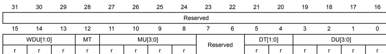
20.6.2 RTC date register (RTC_DR)
The RTC_DR is the calendar date shadow register. This register must be written in initialization mode only. Refer to Calendar initialization and configuration on page 513 and Reading the calendar on page 514 .
Address offset: 0x04
Power-on reset value: 0x0000 2101
System reset: 0x0000 2101 when BYPSHAD = 0. Not affected when BYPSHAD = 1.
| 31 | 30 | 29 | 28 | 27 | 26 | 25 | 24 | 23 | 22 | 21 | 20 | 19 | 18 | 17 | 16 |
|---|---|---|---|---|---|---|---|---|---|---|---|---|---|---|---|
| Reserved | YT[3:0] | YU[3:0] | |||||||||||||
| rw | rw | rw | rw | rw | rw | rw | rw | ||||||||
| 15 | 14 | 13 | 12 | 11 | 10 | 9 | 8 | 7 | 6 | 5 | 4 | 3 | 2 | 1 | 0 |
| WDU[2:0] | MT | MU[3:0] | Reserved | DT[1:0] | DU[3:0] | ||||||||||
| rw | rw | rw | rw | rw | rw | rw | rw | rw | rw | rw | rw | rw | rw | ||
Bits 31-24 Reserved
Bits 23:20 YT[3:0] : Year tens in BCD format
Bits 19:16 YU[3:0] : Year units in BCD format
Bits 15:13 WDU[2:0] : Week day units
000: forbidden
001: Monday
...
111: Sunday
Bit 12 MT : Month tens in BCD format
Bits 11:8 MU : Month units in BCD format
Bits 7:6 Reserved, must be kept at reset value.
Bits 5:4 DT[1:0] : Date tens in BCD format
Bits 3:0 DU[3:0] : Date units in BCD format
Note: This register is write protected. The write access procedure is described in RTC register write protection on page 513 .
20.6.3 RTC control register (RTC_CR)
Address offset: 0x08
Power-on reset value: 0x0000 0000
System reset: not affected
| 31 | 30 | 29 | 28 | 27 | 26 | 25 | 24 | 23 | 22 | 21 | 20 | 19 | 18 | 17 | 16 |
|---|---|---|---|---|---|---|---|---|---|---|---|---|---|---|---|
| Reserved | COE | OSEL[1:0] | POL | COSEL | BKP | SUB1H | ADD1H | ||||||||
| rw | rw | rw | rw | rw | w | w | |||||||||
| 15 | 14 | 13 | 12 | 11 | 10 | 9 | 8 | 7 | 6 | 5 | 4 | 3 | 2 | 1 | 0 |
| TSIE | WUTIE | ALRBIE | ALRAIE | TSE | WUTE | ALRBE | ALRAE | DCE | FMT | BYPSHAD | REFCKON | TSEDGE | WUCKSEL[2:0] | ||
| rw | rw | rw | rw | rw | rw | rw | rw | rw | rw | rw | rw | rw | rw | rw | rw |
Bits 31:24 Reserved, must be kept at reset value.
Bit 23 COE : Calibration output enable
This bit enables the RTC_CALIB output
0: Calibration output disabled
1: Calibration output enabled
Bits 22:21 OSEL[1:0] : Output selection
These bits are used to select the flag to be routed to RTC_ALARM output
00: Output disabled
01: Alarm A output enabled
10: Alarm B output enabled
11: Wakeup output enabled
Bit 20 POL : Output polarity
This bit is used to configure the polarity of RTC_ALARM output
0: The pin is high when ALRAF/ALRBF/WUTF is asserted (depending on OSEL[1:0])
1: The pin is low when ALRAF/ALRBF/WUTF is asserted (depending on OSEL[1:0]).
Bit 19 COSEL : Calibration output selection
This bit is available in Cat.2, Cat.3, Cat.4, Cat.5 and Cat.6 devices only.
When COE=1, this bit selects which signal is output on RTC_CALIB.
0: Calibration output is 512 Hz
1: Calibration output is 1 Hz
These frequencies are valid for RTCCLK at 32.768 kHz and prescalers at their default values (PREDIV_A=127 and PREDIV_S=255). Refer to Section 20.3.14: Calibration clock output
Bit 18 BKP : Backup
This bit can be written by the user to memorize whether the daylight saving time change has been performed or not.
Bit 17 SUB1H : Subtract 1 hour (winter time change)
When this bit is, 1 hour is subtracted to the calendar time if the current hour is not 0. This bit is always read as 0.
Setting this bit has no effect when current hour is 0.
0: No effect
1: Subtracts 1 hour to the current time. This can be used for winter time change outside initialization mode.
Bit 16 ADD1H : Add 1 hour (summer time change)
When this bit is set, 1 hour is added to the calendar time. This bit is always read as 0.
0: No effect
1: Adds 1 hour to the current time. This can be used for summer time change outside initialization mode.
Bit 15 TSIE : Timestamp interrupt enable
0: Timestamp Interrupt disable
1: Timestamp Interrupt enable
Bit 14 WUTIE : Wakeup timer interrupt enable
0: Wakeup timer interrupt disabled
1: Wakeup timer interrupt enabled
Bit 13 ALRBIE : Alarm B interrupt enable
0: Alarm B Interrupt disable
1: Alarm B Interrupt enable
Bit 12 ALRAIE : Alarm A interrupt enable
0: Alarm A interrupt disabled
1: Alarm A interrupt enabled
Bit 11 TSE : Time stamp enable
0: Time stamp disable
1: Time stamp enable
Bit 10 WUTE : Wakeup timer enable
0: Wakeup timer disabled
1: Wakeup timer enabled
Note: When the wakeup timer is disabled, wait for WUTWF=1 before enabling it again.
Bit 9 ALRBE : Alarm B enable
0: Alarm B disabled
1: Alarm B enabled
Bit 8 ALRAE : Alarm A enable
0: Alarm A disabled
1: Alarm A enabled
Bit 7 DCE : Coarse digital calibration enable
0: Digital calibration disabled
1: Digital calibration enabled
PREDIV_A must be 6 or greater
Bit 6 FMT : Hour format
0: 24 hour/day format
1: AM/PM hour format
Bit 5 BYPSHAD : Bypass the shadow registers
This bit is available on Cat.2, Cat.3, Cat.4, Cat.5 and Cat.6 devices only.
0: Calendar values (when reading from RTC_SSR, RTC_TR, and RTC_DR) are taken from the shadow registers, which are updated once every two RTCCLK cycles.
1: Calendar values (when reading from RTC_SSR, RTC_TR, and RTC_DR) are taken directly from the calendar counters.
Note: If the frequency of the APB1 clock is less than seven times the frequency of RTCCLK, BYPSHAD must be set to '1'.
Bit 4 REFCKON : Reference clock detection enable (50 or 60 Hz)
0: Reference clock detection disabled
1: Reference clock detection enabled
Note: PREDIV_S must be 0x00FF.
Bit 3 TSEDGE : Timestamp event active edge
0: TIMESTAMP rising edge generates a timestamp event
1: TIMESTAMP falling edge generates a timestamp event
TSE must be reset when TSEDGE is changed to avoid unwanted TSF setting.
Bits 2:0 WUCKSEL[2:0] : Wakeup clock selection
000: RTC/16 clock is selected
001: RTC/8 clock is selected
010: RTC/4 clock is selected
011: RTC/2 clock is selected
10x: ck_spre (usually 1 Hz) clock is selected
11x: ck_spre (usually 1 Hz) clock is selected and \( 2^{16} \) is added to the WUT counter value (see note below)
Note: WUT = Wakeup unit counter value. WUT = (0x0000 to 0xFFFF) + 0x10000 added when WUCKSEL[2:1 = 11].
Bits 7, 6 and 4 of this register can be written in initialization mode only (RTC_ISR/INITF = 1).
Bits 2 to 0 of this register can be written only when RTC_CR WUTE bit = 0 and RTC_ISR WUTWF bit = 1.
It is recommended not to change the hour during the calendar hour increment as it could mask the incrementation of the calendar hour.
ADD1H and SUB1H changes are effective in the next second.
To avoid spurious setting of TSF, TSE must be reset when TSEDGE is changed.
This register is write protected. The write access procedure is described in RTC register write protection on page 513 .
20.6.4 RTC initialization and status register (RTC_ISR)
Address offset: 0x0C
Power-on reset value: 0x0000 0007
System reset value: Not affected except INIT, INITF and RSF which are cleared to 0.
| 31 | 30 | 29 | 28 | 27 | 26 | 25 | 24 | 23 | 22 | 21 | 20 | 19 | 18 | 17 | 16 |
|---|---|---|---|---|---|---|---|---|---|---|---|---|---|---|---|
| Reserved | RECAL PF | ||||||||||||||
| r | |||||||||||||||
| 15 | 14 | 13 | 12 | 11 | 10 | 9 | 8 | 7 | 6 | 5 | 4 | 3 | 2 | 1 | 0 |
| TAMP 3F | TAMP 2F | TAMP 1F | TSOVF | TSF | WUTF | ALRBF | ALRAF | INIT | INITF | RSF | INITS | SHPF | WUT WF | ALRB WF | ALRA WF |
| rc_w0 | rc_w0 | rc_w0 | rc_w0 | rc_w0 | rc_w0 | rc_w0 | rc_w0 | rw | r | rc_w0 | r | r | r | r | r |
Bits 31:17 Reserved
Bit 16 RECALPF : Recalibration pending Flag
The RECALPF status flag is automatically set to '1' when software writes to the RTC_CALR register, indicating that the RTC_CALR register is blocked. When the new calibration settings are taken into account, this bit returns to '0'. Refer to Section : Re-calibration on-the-fly .
Bit 15 TAMP3F : TAMPER3 detection flag
This flag is set by hardware when a tamper detection event is detected on tamper input 3. It is cleared by software writing 0.
Bit 14 TAMP2F : TAMPER2 detection flag
This flag is set by hardware when a tamper detection event is detected on tamper input 2. It is cleared by software writing 0.
Bit 13 TAMP1F : Tamper detection flag
This flag is set by hardware when a tamper detection event is detected. It is cleared by software writing 0.
Bit 12 TSOVF : Timestamp overflow flag
This flag is set by hardware when a timestamp event occurs while TSF is already set. This flag is cleared by software by writing 0. It is recommended to check and then clear TSOVF only after clearing the TSF bit. Otherwise, an overflow might not be noticed if a timestamp event occurs immediately before the TSF bit is cleared.
Bit 11 TSF : Timestamp flag
This flag is set by hardware when a timestamp event occurs. This flag is cleared by software by writing 0.
Bit 10 WUTF : Wakeup timer flag
This flag is set by hardware when the wakeup auto-reload counter reaches 0. This flag is cleared by software by writing 0. This flag must be cleared by software at least 1.5 RTCCLK periods before WUTF is set to 1 again.
Bit 9 ALRBF : Alarm B flag
This flag is set by hardware when the time/date registers (RTC_TR and RTC_DR) match the Alarm B register (RTC_ALRMBR). This flag is cleared by software by writing 0.
Bit 8 ALRAF : Alarm A flag
This flag is set by hardware when the time/date registers (RTC_TR and RTC_DR) match the Alarm A register (RTC_ALRMAR). This flag is cleared by software by writing 0.
Bit 7 INIT : Initialization mode
0: Free running mode
1: Initialization mode used to program time and date register (RTC_TR and RTC_DR), and prescaler register (RTC_PRRER). Counters are stopped and start counting from the new value when INIT is reset.
Bit 6 INITF : Initialization flag
When this bit is set to 1, the RTC is in initialization state, and the time, date and prescaler registers can be updated.
0: Calendar registers update is not allowed
1: Calendar registers update is allowed.
This bit is set by hardware each time the calendar registers are copied into the shadow registers (RTC_SSRx, RTC_TRx and RTC_DRx). This bit is cleared by hardware in initialization mode, while a shift operation is pending (SHPF=1), or when in bypass shadow register mode (BYPSHAD=1). This bit can also be cleared by software.
0: Calendar shadow registers not yet synchronized
1: Calendar shadow registers synchronized
Bit 4 INITS: Initialization status flagThis bit is set by hardware when the calendar year field is different from 0 (power-on reset value state).
0: Calendar has not been initialized
1: Calendar has been initialized
Bit 3 SHPF: Shift operation pending0: No shift operation is pending
1: A shift operation is pending
This flag is set by hardware as soon as a shift operation is initiated by a write to the RTC_SHIFTR. It is cleared by hardware when the corresponding shift operation has been executed. Writing to SHPF has no effect.
Bit 3 Reserved, must be kept at reset value. Bit 2 WUTWF: Wakeup timer write flagThis bit is set by hardware up to 2 RTCCLK cycles after the WUTE bit has been set to 0 in RTC_CR, and is cleared up to 2 RTCCLK cycles after the WUTE bit has been set to 1. The wakeup timer values can be changed when WUTE bit is cleared and WUTWF is set.
0: Wakeup timer configuration update not allowed
1: Wakeup timer configuration update allowed
Bit 1 ALRBWF: Alarm B write flagThis bit is set by hardware when Alarm B values can be changed, after the ALRBIE bit has been set to 0 in RTC_CR.
It is cleared by hardware in initialization mode.
0: Alarm B update not allowed
1: Alarm B update allowed.
Bit 0 ALRAWF: Alarm A write flagThis bit is set by hardware when Alarm A values can be changed, after the ALRAE bit has been set to 0 in RTC_CR.
It is cleared by hardware in initialization mode.
0: Alarm A update not allowed
1: Alarm A update allowed
Note: The ALRAF, ALRBF, WUTF and TSF bits are cleared 2 APB clock cycles after programming them to 0.
This register is write protected (except for RTC_ISR[13:8] bits). The write access procedure is described in RTC register write protection on page 513 .
20.6.5 RTC prescaler register (RTC_PRER)
Address offset: 0x10
Power-on reset value: 0x007F 00FF
System reset: not affected
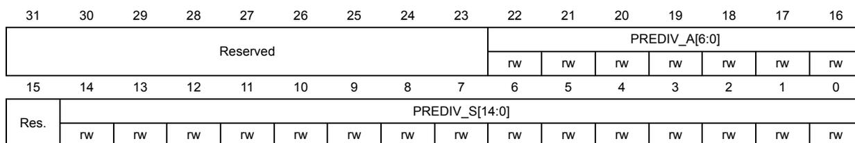
| 31 | 30 | 29 | 28 | 27 | 26 | 25 | 24 | 23 | 22 | 21 | 20 | 19 | 18 | 17 | 16 | |
| Reserved | Res. | PREDIV_A[6:0] | ||||||||||||||
| rw | rw | rw | rw | rw | rw | rw | ||||||||||
| 15 | 14 | 13 | 12 | 11 | 10 | 9 | 8 | 7 | 6 | 5 | 4 | 3 | 2 | 1 | 0 | |
| Res. | PREDIV_S[14:0] | |||||||||||||||
| rw | rw | rw | rw | rw | rw | rw | rw | rw | rw | rw | rw | rw | rw | rw | ||
Bits 31:24 Reserved
Bit 23 Reserved, must be kept at reset value.
Bits 22:16
PREDIV_A[6:0]
: Asynchronous prescaler factor
This is the asynchronous division factor:
\(
ck\_apre\ frequency = RTCCLK\ frequency / (PREDIV\_A + 1)
\)
Bit 15 Reserved, must be kept at reset value.
Bits 14:0
PREDIV_S[14:0]
: Synchronous prescaler factor
This is the synchronous division factor:
\(
ck\_spre\ frequency = ck\_apre\ frequency / (PREDIV\_S + 1)
\)
Note: PREDIV[14:13] are reserved in Cat.1 devices.
Note: This register must be written in initialization mode only. The initialization must be performed in two separate write accesses. Refer to Calendar initialization and configuration on page 513
This register is write protected. The write access procedure is described in RTC register write protection on page 513 .
20.6.6 RTC wakeup timer register (RTC_WUTR)
Address offset: 0x14
Power-on reset value: 0x0000 FFFF
System reset: not affected
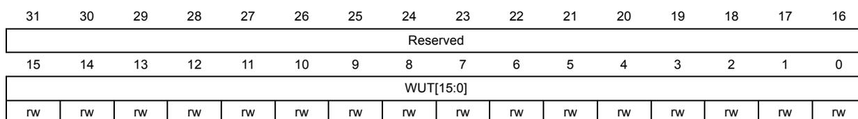
| 31 | 30 | 29 | 28 | 27 | 26 | 25 | 24 | 23 | 22 | 21 | 20 | 19 | 18 | 17 | 16 |
| Reserved | |||||||||||||||
| 15 | 14 | 13 | 12 | 11 | 10 | 9 | 8 | 7 | 6 | 5 | 4 | 3 | 2 | 1 | 0 |
| WUT[15:0] | |||||||||||||||
| rw | rw | rw | rw | rw | rw | rw | rw | rw | rw | rw | rw | rw | rw | rw | rw |
Bits 31:16 Reserved
Bits 15:0 WUT[15:0] : Wakeup auto-reload value bits
When the wakeup timer is enabled (WUTE set to 1), the WUTF flag is set every (WUT[15:0] + 1) ck_wut cycles. The ck_wut period is selected through WUCKSEL[2:0] bits of the RTC_CR register
When WUCKSEL[2] = 1, the wakeup timer becomes 17-bits and WUCKSEL[1] effectively becomes WUT[16] the most-significant bit to be reloaded into the timer.
Note: The first assertion of WUTF occurs (WUT+1) ck_wut cycles after WUTE is set. Setting WUT[15:0] to 0x0000 with WUCKSEL[2:0] =011 (RTCCLK/2) is forbidden.
Note: This register can be written only when WUTWF is set to 1 in RTC_ISR.
This register is write protected. The write access procedure is described in RTC register write protection on page 513 .
20.6.7 RTC calibration register (RTC_CALIBR)
Address offset: 0x18
Power-on reset value: 0x0000 0000
System reset: not affected
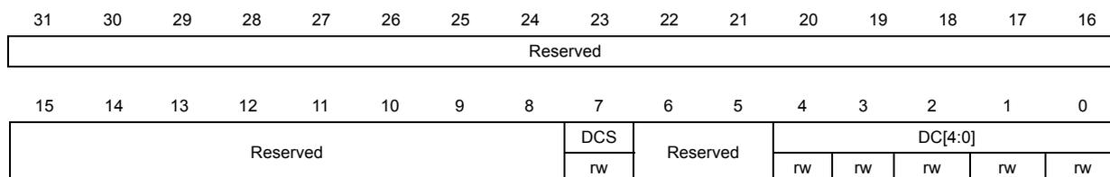
| 31 | 30 | 29 | 28 | 27 | 26 | 25 | 24 | 23 | 22 | 21 | 20 | 19 | 18 | 17 | 16 |
| Reserved | |||||||||||||||
| 15 | 14 | 13 | 12 | 11 | 10 | 9 | 8 | 7 | 6 | 5 | 4 | 3 | 2 | 1 | 0 |
| Reserved | DCS | Reserved | DC[4:0] | ||||||||||||
| rw | rw | rw | rw | rw | rw | ||||||||||
Bits 31:8 Reserved
Bit 7 DCS : Digital calibration sign
- 0: Positive calibration: calendar update frequency is increased
- 1: Negative calibration: calendar update frequency is decreased
Bits 6:5 Reserved, must be kept at reset value.
Bits 4:0 DC[4:0] : Digital calibration
DCS = 0 (positive calibration)
- 00000: + 0 ppm
- 00001: + 4 ppm (rounded value)
- 00010: + 8 ppm (rounded value)
- ..
- 11111: + 126 ppm (rounded value)
DCS = 1 (negative calibration)
- 00000: -0 ppm
- 00001: -2 ppm (rounded value)
- 00010: -4 ppm (rounded value)
- ..
- 11111: -63 ppm (rounded value)
Refer to Case of RTCCLK=32.768 kHz and PREDIV_A+1=128 on page 518 for the exact step value.
Note:
This register can be written in initialization mode only (RTC_ISR/INITF = '1').
This register is write protected. The write access procedure is described in
RTC register write protection on page 513
.
20.6.8 RTC alarm A register (RTC_ALRMAR)
Address offset: 0x1C
Power-on reset value: 0x0000 0000
System reset: not affected
| 31 | 30 | 29 | 28 | 27 | 26 | 25 | 24 | 23 | 22 | 21 | 20 | 19 | 18 | 17 | 16 |
|---|---|---|---|---|---|---|---|---|---|---|---|---|---|---|---|
| MSK4 | WDSEL | DT[1:0] | DU[3:0] | MSK3 | PM | HT[1:0] | HU[3:0] | ||||||||
| rw | rw | rw | rw | rw | rw | rw | rw | rw | rw | rw | rw | rw | rw | rw | rw |
| 15 | 14 | 13 | 12 | 11 | 10 | 9 | 8 | 7 | 6 | 5 | 4 | 3 | 2 | 1 | 0 |
| MSK2 | MNT[2:0] | MNU[3:0] | MSK1 | ST[2:0] | SU[3:0] | ||||||||||
| rw | rw | rw | rw | rw | rw | rw | rw | rw | rw | rw | rw | rw | rw | rw | rw |
Bit 31 MSK4 : Alarm A date mask
- 0: Alarm A set if the date/day match
- 1: Date/day don't care in Alarm A comparison
Bit 30 WDSEL : Week day selection
- 0: DU[3:0] represents the date units
- 1: DU[3:0] represents the week day. DT[1:0] is don't care.
Bits 29:28 DT[1:0] : Date tens in BCD format.
Bits 27:24 DU[3:0] : Date units or day in BCD format.
Bit 23 MSK3 : Alarm A hours mask
- 0: Alarm A set if the hours match
- 1: Hours don't care in Alarm A comparison
Bit 22 PM : AM/PM notation
- 0: AM or 24-hour format
- 1: PM
Bits 21:20 HT[1:0] : Hour tens in BCD format.
Bits 19:16 HU[3:0] : Hour units in BCD format.
Bit 15 MSK2 : Alarm A minutes mask
- 0: Alarm A set if the minutes match
- 1: Minutes don't care in Alarm A comparison
Bits 14:12 MNT[2:0] : Minute tens in BCD format.
Bits 11:8 MNU[3:0] : Minute units in BCD format.
Bit 7 MSK1 : Alarm A seconds mask
- 0: Alarm A set if the seconds match
- 1: Seconds don't care in Alarm A comparison
Bits 6:4 ST[2:0] : Second tens in BCD format.
Bits 3:0 SU[3:0] : Second units in BCD format.
Note: This register can be written only when ALRAWF is set to 1 in RTC_ISR, or in initialization mode.
This register is write protected. The write access procedure is described in RTC register write protection on page 513 .
20.6.9 RTC alarm B register (RTC_ALRMBR)
Address offset: 0x20
Power-on reset value: 0x0000 0000
System reset: not affected
| 31 | 30 | 29 | 28 | 27 | 26 | 25 | 24 | 23 | 22 | 21 | 20 | 19 | 18 | 17 | 16 |
|---|---|---|---|---|---|---|---|---|---|---|---|---|---|---|---|
| MSK4 | WDSEL | DT[1:0] | DU[3:0] | MSK3 | PM | HT[1:0] | HU[3:0] | ||||||||
| rw | rw | rw | rw | rw | rw | rw | rw | rw | rw | rw | rw | rw | rw | rw | rw |
| 15 | 14 | 13 | 12 | 11 | 10 | 9 | 8 | 7 | 6 | 5 | 4 | 3 | 2 | 1 | 0 |
|---|---|---|---|---|---|---|---|---|---|---|---|---|---|---|---|
| MSK2 | MNT[2:0] | MNU[3:0] | MSK1 | ST[2:0] | SU[3:0] | ||||||||||
| rw | rw | rw | rw | rw | rw | rw | rw | rw | rw | rw | rw | rw | rw | rw | rw |
Bit 31 MSK4 : Alarm B date mask
0: Alarm B set if the date and day match
1: Date and day don't care in Alarm B comparison
Bit 30 WDSEL : Week day selection
0: DU[3:0] represents the date units
1: DU[3:0] represents the week day. DT[1:0] is don't care.
Bits 29:28 DT[1:0] : Date tens in BCD format
Bits 27:24 DU[3:0] : Date units or day in BCD format
Bit 23 MSK3 : Alarm B hours mask
0: Alarm B set if the hours match
1: Hours don't care in Alarm B comparison
Bit 22 PM : AM/PM notation
0: AM or 24-hour format
1: PM
Bits 21:20 HT[1:0] : Hour tens in BCD format
Bits 19:16 HU[3:0] : Hour units in BCD format
Bit 15 MSK2 : Alarm B minutes mask
0: Alarm B set if the minutes match
1: Minutes don't care in Alarm B comparison
Bits 14:12 MNT[2:0] : Minute tens in BCD format
Bits 11:8 MNU[3:0] : Minute units in BCD format
Bit 7 MSK1 : Alarm B seconds mask
0: Alarm B set if the seconds match
1: Seconds don't care in Alarm B comparison
Bits 6:4 ST[2:0] : Second tens in BCD format
Bits 3:0 SU[3:0] : Second units in BCD format
Note: This register can be written only when ALRBWF is set to 1 in RTC_ISR, or in initialization mode.
This register is write protected. The write access procedure is described in RTC register write protection on page 513 .
20.6.10 RTC write protection register (RTC_WPR)
Address offset: 0x24
Power-on reset value: 0x0000 0000
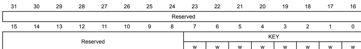
| 31 | 30 | 29 | 28 | 27 | 26 | 25 | 24 | 23 | 22 | 21 | 20 | 19 | 18 | 17 | 16 |
| Reserved | |||||||||||||||
| 15 | 14 | 13 | 12 | 11 | 10 | 9 | 8 | 7 | 6 | 5 | 4 | 3 | 2 | 1 | 0 |
| Reserved | KEY | ||||||||||||||
| w | w | w | w | w | w | w | w | ||||||||
Bits 31:8 Reserved, must be kept at reset value.
Bits 7:0 KEY : Write protection key
This byte is written by software.
Reading this byte always returns 0x00.
Refer to RTC register write protection for a description of how to unlock RTC register write protection.
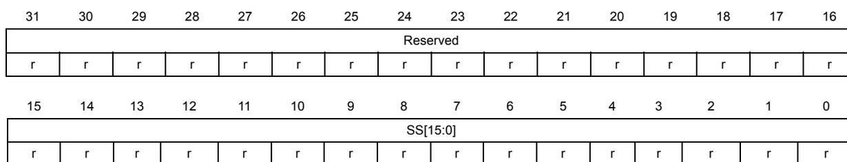
20.6.11 RTC sub second register (RTC_SSR)
The RTC_SSR register is available only on Cat.2, Cat.3, Cat.4, Cat.5 and Cat.6 devices.
Address offset: 0x28
Power-on reset value: 0x0000 0000
System reset: 0x0000 0000 when BYPSHAD = 0. Not affected when BYPSHAD = 1.
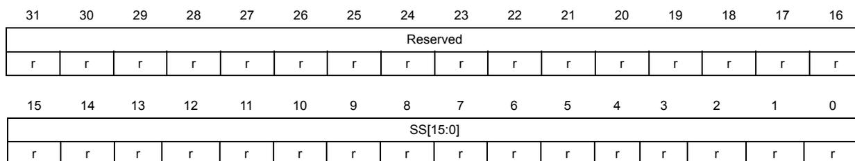
| 31 | 30 | 29 | 28 | 27 | 26 | 25 | 24 | 23 | 22 | 21 | 20 | 19 | 18 | 17 | 16 |
| Reserved | |||||||||||||||
| r | r | r | r | r | r | r | r | r | r | r | r | r | r | r | r |
| 15 | 14 | 13 | 12 | 11 | 10 | 9 | 8 | 7 | 6 | 5 | 4 | 3 | 2 | 1 | 0 |
| SS[15:0] | |||||||||||||||
| r | r | r | r | r | r | r | r | r | r | r | r | r | r | r | r |
Bits 31:16 Reserved
Bits 15:0 SS : Sub second value
SS[15:0] is the value in the synchronous prescaler's counter. The fraction of a second is given by the formula below:
Second fraction = ( PREDIV_S - SS ) / ( PREDIV_S + 1 )
Note: SS can be larger than PREDIV_S only after a shift operation. In that case, the correct time/date is one second less than as indicated by RTC_TR/RTC_DR.
20.6.12 RTC shift control register (RTC_SHIFTR)
The RTC_SHIFTR register is available only in Cat.2, Cat.3, Cat.4, Cat.5 and Cat.6 devices.
Address offset: 0x2C
Power-on reset value: 0x0000 0000
System reset: not affected
| 31 | 30 | 29 | 28 | 27 | 26 | 25 | 24 | 23 | 22 | 21 | 20 | 19 | 18 | 17 | 16 |
|---|---|---|---|---|---|---|---|---|---|---|---|---|---|---|---|
| ADD1S | Reserved | ||||||||||||||
| w | r | r | r | r | r | r | r | r | r | r | r | r | r | r | r |
| 15 | 14 | 13 | 12 | 11 | 10 | 9 | 8 | 7 | 6 | 5 | 4 | 3 | 2 | 1 | 0 |
|---|---|---|---|---|---|---|---|---|---|---|---|---|---|---|---|
| Res. | SUBFS[14:0] | ||||||||||||||
| r | w | w | w | w | w | w | w | w | w | w | w | w | w | w | w |
Bit 31 ADD1S: Add one second
0: No effect
1: Add one second to the clock/calendar
This bit is write only and is always read as zero. Writing to this bit has no effect when a shift operation is pending (when SHPF=1, in RTC_ISR).
This function is intended to be used with SUBFS (see description below) in order to effectively add a fraction of a second to the clock in an atomic operation.
Bits 30:15 Reserved
Bits 14:0 SUBFS: Subtract a fraction of a second
These bits are write only and is always read as zero. Writing to this bit has no effect when a shift operation is pending (when SHPF=1, in RTC_ISR).
The value which is written to SUBFS is added to the synchronous prescaler's counter. Since this counter counts down, this operation effectively subtracts from (delays) the clock by:
A fraction of a second can effectively be added to the clock (advancing the clock) when the ADD1S function is used in conjunction with SUBFS, effectively advancing the clock by:
Note: Writing to SUBFS causes RSF to be cleared. Software can then wait until RSF=1 to be sure that the shadow registers have been updated with the shifted time.
Refer to Section 20.3.8: RTC synchronization (Cat.2, Cat.3, Cat.4, Cat.5 and Cat.6 devices only) .
Note: This register is write protected. The write access procedure is described in RTC register write protection on page 513
20.6.13 RTC time stamp time register (RTC_TSTR)
Address offset: 0x30
Power-on reset value: 0x0000 0000
System reset: not affected
| 31 | 30 | 29 | 28 | 27 | 26 | 25 | 24 | 23 | 22 | 21 | 20 | 19 | 18 | 17 | 16 |
| Reserved | PM | HT[1:0] | HU[3:0] | ||||||||||||
| r | r | r | r | r | r | r | r | ||||||||
| 15 | 14 | 13 | 12 | 11 | 10 | 9 | 8 | 7 | 6 | 5 | 4 | 3 | 2 | 1 | 0 |
| Res. | MNT[2:0] | MNU[3:0] | Res. | ST[2:0] | SU[3:0] | ||||||||||
| r | r | r | r | r | r | r | r | r | r | r | r | r | r | r | r |
Bits 31:23 Reserved, must be kept at reset value.
Bit 22 PM : AM/PM notation
0: AM or 24-hour format
1: PM
Bits 21:20 HT[1:0] : Hour tens in BCD format.
Bits 19:16 HU[3:0] : Hour units in BCD format.
Bit 15 Reserved, must be kept at reset value.
Bits 14:12 MNT[2:0] : Minute tens in BCD format.
Bits 11:8 MNU[3:0] : Minute units in BCD format.
Bit 7 Reserved, must be kept at reset value.
Bits 6:4 ST[2:0] : Second tens in BCD format.
Bits 3:0 SU[3:0] : Second units in BCD format.
Note: The content of this register is valid only when TSF is set to 1 in RTC_ISR. It is cleared when TSF bit is reset.
20.6.14 RTC time stamp date register (RTC_TSDR)
Address offset: 0x34
Power-on reset value: 0x0000 0000
System reset: not affected
| 31 | 30 | 29 | 28 | 27 | 26 | 25 | 24 | 23 | 22 | 21 | 20 | 19 | 18 | 17 | 16 | |
| Reserved | ||||||||||||||||
| 15 | 14 | 13 | 12 | 11 | 10 | 9 | 8 | 7 | 6 | 5 | 4 | 3 | 2 | 1 | 0 | |
| WDU[1:0] | MT | MU[3:0] | Reserved | DT[1:0] | DU[3:0] | |||||||||||
| r | r | r | r | r | r | r | r | r | r | r | r | r | r | r | ||
Bits 31:16 Reserved, must be kept at reset value.
Bits 15:13 WDU[1:0] : Week day units
Bit 12 MT : Month tens in BCD format
Bits 11:8 MU[3:0] : Month units in BCD format
Bits 7:6 Reserved, must be kept at reset value.
Bits 5:4 DT[1:0] : Date tens in BCD format
Bit 3:0 DU[3:0] : Date units in BCD format
Note: The content of this register is valid only when TSF is set to 1 in RTC_ISR. It is cleared when TSF bit is reset.
20.6.15 RTC timestamp sub second register (RTC_TSSSR)
The RTC_TSSSR register is available only on Cat.2, Cat.3, Cat.4, Cat.5 and Cat.6 devices.
Address offset: 0x38
Power-on reset value: 0x0000 0000
System reset: not affected
| 31 | 30 | 29 | 28 | 27 | 26 | 25 | 24 | 23 | 22 | 21 | 20 | 19 | 18 | 17 | 16 |
| Reserved | |||||||||||||||
| r | r | r | r | r | r | r | r | r | r | r | r | r | r | r | r |
| 15 | 14 | 13 | 12 | 11 | 10 | 9 | 8 | 7 | 6 | 5 | 4 | 3 | 2 | 1 | 0 |
| SS[15:0] | |||||||||||||||
| r | r | r | r | r | r | r | r | r | r | r | r | r | r | r | r |
Bits 31:16 Reserved
Bits 15:0 SS : Sub second value
SS[15:0] is the value of the synchronous prescaler's counter when the timestamp event occurred.
Note: The content of this register is valid only when RTC_ISR/TSF is set. It is cleared when the RTC_ISR/TSF bit is reset.
20.6.16 RTC calibration register (RTC_CALR)
The RTC_CALR register is available only on Cat.2, Cat.3, Cat.4, Cat.5 and Cat.6 devices.
Address offset: 0x3C
Power-on reset value: 0x0000 0000
System reset: not affected
| 31 | 30 | 29 | 28 | 27 | 26 | 25 | 24 | 23 | 22 | 21 | 20 | 19 | 18 | 17 | 16 |
|---|---|---|---|---|---|---|---|---|---|---|---|---|---|---|---|
| Reserved | |||||||||||||||
| r | r | r | r | r | r | r | r | r | r | r | r | r | r | r | r |
| 15 | 14 | 13 | 12 | 11 | 10 | 9 | 8 | 7 | 6 | 5 | 4 | 3 | 2 | 1 | 0 |
|---|---|---|---|---|---|---|---|---|---|---|---|---|---|---|---|
| CALP | CALW8 | CALW16 | Reserved | CALM[8:0] | |||||||||||
| rw | rw | rw | r | r | r | r | rw | rw | rw | rw | rw | rw | rw | rw | rw |
Bits 31:16 Reserved
Bit 15 CALP : Increase frequency of RTC by 488.5 ppm
0: No RTCCLK pulses are added.
1: One RTCCLK pulse is effectively inserted every \( 2^{11} \) pulses (frequency increased by 488.5 ppm).
This feature is intended to be used in conjunction with CALM, which lowers the frequency of the calendar with a fine resolution. if the input frequency is 32768 Hz, the number of RTCCLK pulses added during a 32-second window is calculated as follows: \( (512 * CALP) - CALM \) .
Refer to Section 20.3.11: RTC smooth digital calibration (Cat.2, Cat.3, Cat.4, Cat.5 and Cat.6 devices only) .
Bit 14 CALW8 : Use an 8-second calibration cycle period
When CALW8 is set to '1', the 8-second calibration cycle period is selected.
CALM[1:0] are stuck at "00" when CALW8='1'.
Refer to Section 20.3.11: RTC smooth digital calibration (Cat.2, Cat.3, Cat.4, Cat.5 and Cat.6 devices only) .
Bit 13 CALW16 : Use a 16-second calibration cycle period
When CALW16 is set to '1', the 16-second calibration cycle period is selected. This bit must not be set to '1' if CALW8=1.
Note: CALM[0] is stuck at '0' when CALW16='1'.
Refer to Section 20.3.11: RTC smooth digital calibration (Cat.2, Cat.3, Cat.4, Cat.5 and Cat.6 devices only) .
Bits 12:9 Reserved
Bits 8:0 CALM[8:0] : Calibration minus
The frequency of the calendar is reduced by masking CALM out of \( 2^{20} \) RTCCLK pulses (32 seconds if the input frequency is 32768 Hz). This decreases the frequency of the calendar with a resolution of 0.9537 ppm.
To increase the frequency of the calendar, this feature should be used in conjunction with CALP.
Note: This register is write protected. The write access procedure is described in RTC register write protection on page 513 .
20.6.17 RTC tamper and alternate function configuration register (RTC_TAFCR)
Address offset: 0x40
Power-on reset value: 0x0000 0000
System reset: not affected
| 31 | 30 | 29 | 28 | 27 | 26 | 25 | 24 | 23 | 22 | 21 | 20 | 19 | 18 | 17 | 16 |
|---|---|---|---|---|---|---|---|---|---|---|---|---|---|---|---|
| Reserved | ALARMOUT TYPE | Reserved | |||||||||||||
| rw | |||||||||||||||
| 15 | 14 | 13 | 12 | 11 | 10 | 9 | 8 | 7 | 6 | 5 | 4 | 3 | 2 | 1 | 0 |
| TAMP- PUDIS | TAMP- PRCH[1:0] | TAMPFLT[1:0] | TAMPFREQ[2:0] | TAMP TS | TAMP 3TRG | TAMP 3E | TAMP 2TRG | TAMP 2E | TAMPIE | TAMP 1TRG | TAMP 1E | ||||
| rw | rw | rw | rw | rw | rw | rw | rw | rw | rw | rw | rw | rw | rw | rw | rw |
Bits 31:19 Reserved. Always read as 0.
Bit 18 ALARMOUTTYPE : RTC_ALARM output type
0: ALARM_AF0 is an open-drain output
1: ALARM_AF0 is a push-pull output
Bit 17:16 Reserved. Always read as 0.
Bit 15 TAMPPUDIS : TAMPER pull-up disable
This bit determines if each of the tamper pins are pre-charged before each sample.
0: Precharge tamper pins before sampling (enable internal pull-up)
1: Disable precharge of tamper pins
Note: This bit is available in Cat.2, Cat.3, Cat.4, Cat.5 and Cat.6 devices only
Bits 14:13 TAMPPRCH[1:0] : Tamper precharge duration
These bits determine the duration of time during which the pull-up/is activated before each sample. TAMPPRCH is valid for each of the tamper inputs.
0x0: 1 RTCCLK cycle
0x1: 2 RTCCLK cycles
0x2: 4 RTCCLK cycles
0x3: 8 RTCCLK cycles
Note: This bits is available in Cat.2, Cat.3, Cat.4, Cat.5 and Cat.6 devices only
Bits 12:11 TAMPFLT[1:0] : Tamper filter count
These bits determine the number of consecutive samples at the specified level (TAMP*TRG) necessary to activate a Tamper event. TAMPFLT is valid for each of the tamper inputs.
0x0: Tamper is activated on edge of tamper input transitions to the active level (no internal pull-up on tamper input).
0x1: Tamper is activated after 2 consecutive samples at the active level.
0x2: Tamper is activated after 4 consecutive samples at the active level.
0x3: Tamper is activated after 8 consecutive samples at the active level.
Note: This bit is available in Cat.2, Cat.3, Cat.4, Cat.5 and Cat.6 devices only
Bits 10:8 TAMPFREQ[2:0] : Tamper sampling frequencyDetermines the frequency at which each of the tamper inputs are sampled.
0x0: RTCCLK / 32768 (1 Hz when RTCCLK = 32768 Hz)
0x1: RTCCLK / 16384 (2 Hz when RTCCLK = 32768 Hz)
0x2: RTCCLK / 8192 (4 Hz when RTCCLK = 32768 Hz)
0x3: RTCCLK / 4096 (8 Hz when RTCCLK = 32768 Hz)
0x4: RTCCLK / 2048 (16 Hz when RTCCLK = 32768 Hz)
0x5: RTCCLK / 1024 (32 Hz when RTCCLK = 32768 Hz)
0x6: RTCCLK / 512 (64 Hz when RTCCLK = 32768 Hz)
0x7: RTCCLK / 256 (128 Hz when RTCCLK = 32768 Hz)
Note: These bits are available in Cat.2, Cat.3, Cat.4, Cat.5 and Cat.6 devices only
Bit 7 TAMPTS : Activate timestamp on tamper detection event0: Tamper detection event does not cause a timestamp to be saved
1: Save timestamp on tamper detection event
TAMPTS is valid even if TSE=0 in the RTC_CR register.
Note: This bit is available in Cat.2, Cat.3, Cat.4, Cat.5 and Cat.6 devices only
Bit 6 TAMP3TRG : Active level for tamper 2if TAMPFLT != 00 (Cat.2, Cat.3, Cat.4, Cat.5 and Cat.6 device only):
0: TAMPER3 staying low triggers a tamper detection event.
1: TAMPER3 staying high triggers a tamper detection event.
if TAMPFLT = 00:
0: TAMPER3 rising edge triggers a tamper detection event.
1: TAMPER3 falling edge triggers a tamper detection event.
Bit 5 TAMP3E : Tamper 3 detection enable0: Tamper 3 detection disabled
1: Tamper 3 detection enabled
Bit 4 TAMP2TRG : Active level for tamper 2if TAMPFLT != 00 (Cat.2, Cat.3, Cat.4, Cat.5 and Cat.6 device only):
0: TAMPER2 staying low triggers a tamper detection event.
1: TAMPER2 staying high triggers a tamper detection event.
if TAMPFLT = 00:
0: TAMPER2 rising edge triggers a tamper detection event.
1: TAMPER2 falling edge triggers a tamper detection event.
Note: This bit is available in Cat.2, Cat.3, Cat.4, Cat.5 and Cat.6 devices only
Bit 3 TAMP2E : Tamper 2 detection enable0: Tamper 2 detection disabled
1: Tamper 2 detection enabled
Note: This bit is available in Cat.2, Cat.3, Cat.4, Cat.5 and Cat.6 devices only
Bit 2 TAMPIE : Tamper interrupt enable0: Tamper interrupt disabled
1: Tamper interrupt enabled
Bit 1 TAMP1TRG : Active level for tamper 1
if TAMPFLT != 00 (Cat.2, Cat.3, Cat.4, Cat.5 and Cat.6 device only)
0: TAMPER1 staying low triggers a tamper detection event.
1: TAMPER1 staying high triggers a tamper detection event.
if TAMPFLT = 00 :
0: TAMPER1 rising edge triggers a tamper detection event.
1: TAMPER1 falling edge triggers a tamper detection event.
Caution: When TAMPFLT = 0, TAMPxE must be reset when TAMPxTRG is changed to avoid spuriously setting TAMPxF.
Bit 0 TAMP1E : Tamper 1 detection enable
0: Tamper 1 detection disabled
1: Tamper 1 detection enabled
20.6.18 RTC alarm A sub second register (RTC_ALRMASSR)
The RTC_ALRMASSR register is available in Cat.2, Cat.3, Cat.4, Cat.5 and Cat.6 devices only.
Address offset: 0x44
Power-on reset value: 0x0000 0000
System reset: not affected
| 31 | 30 | 29 | 28 | 27 | 26 | 25 | 24 | 23 | 22 | 21 | 20 | 19 | 18 | 17 | 16 |
|---|---|---|---|---|---|---|---|---|---|---|---|---|---|---|---|
| Reserved | MASKSS[3:0] | Reserved | |||||||||||||
| r | r | r | r | rw | rw | rw | rw | r | r | r | r | r | r | r | r |
| 15 | 14 | 13 | 12 | 11 | 10 | 9 | 8 | 7 | 6 | 5 | 4 | 3 | 2 | 1 | 0 |
|---|---|---|---|---|---|---|---|---|---|---|---|---|---|---|---|
| Reserved | SS[14:0] | ||||||||||||||
| r | rw | rw | rw | rw | rw | rw | rw | rw | rw | rw | rw | rw | w | rw | rw |
Bits 31:28 Reserved
Bits 27:24 MASKSS[3:0] : Mask the most-significant bits starting at this bit
0: No comparison on sub seconds for Alarm A. The alarm is set when the seconds unit is incremented (assuming that the rest of the fields match).
1: SS[14:1] are don't care in Alarm A comparison. Only SS[0] is compared.
2: SS[14:2] are don't care in Alarm A comparison. Only SS[1:0] are compared.
3: SS[14:3] are don't care in Alarm A comparison. Only SS[2:0] are compared.
...
12: SS[14:12] are don't care in Alarm A comparison. SS[11:0] are compared.
13: SS[14:13] are don't care in Alarm A comparison. SS[12:0] are compared.
14: SS[14] is don't care in Alarm A comparison. SS[13:0] are compared.
15: All 15 SS bits are compared and must match to activate alarm.
The overflow bits of the synchronous counter (bits 15) is never compared. This bit can be different from 0 only after a shift operation.
Bits 23:15 Reserved
Bits 14:0 SS[14:0] : Sub seconds value
This value is compared with the contents of the synchronous prescaler's counter to determine if Alarm A is to be activated. Only bits 0 up MASKSS-1 are compared.
Note: This register can be written only when ALRAE is reset in RTC_CR register, or in initialization mode.
This register is write protected. The write access procedure is described in RTC register write protection on page 513
20.6.19 RTC alarm B sub second register (RTC_ALRMBSSR)
The RTC_ALRMBSSR register is available only in Cat.2, Cat.3, Cat.4, Cat.5 and Cat.6 devices.
Address offset: 0x48
Power-on reset value: 0x0000 0000
System reset: not affected
| 31 | 30 | 29 | 28 | 27 | 26 | 25 | 24 | 23 | 22 | 21 | 20 | 19 | 18 | 17 | 16 |
|---|---|---|---|---|---|---|---|---|---|---|---|---|---|---|---|
| Reserved | MASKSS[3:0] | Reserved | |||||||||||||
| r | r | r | r | rw | rw | rw | rw | r | r | r | r | r | r | r | r |
| 15 | 14 | 13 | 12 | 11 | 10 | 9 | 8 | 7 | 6 | 5 | 4 | 3 | 2 | 1 | 0 |
|---|---|---|---|---|---|---|---|---|---|---|---|---|---|---|---|
| Reserved | SS[14:0] | ||||||||||||||
| r | rw | rw | rw | rw | rw | rw | rw | rw | rw | rw | rw | rw | w | rw | rw |
Bits 31:28 Reserved
Bits 27:24 MASKSS[3:0] : Mask the most-significant bits starting at this bit
0x0: No comparison on sub seconds for Alarm B. The alarm is set when the seconds unit is incremented (assuming that the rest of the fields match).
0x1: SS[14:1] are don't care in Alarm B comparison. Only SS[0] is compared.
0x2: SS[14:2] are don't care in Alarm B comparison. Only SS[1:0] are compared.
0x3: SS[14:3] are don't care in Alarm B comparison. Only SS[2:0] are compared.
...
0xC: SS[14:12] are don't care in Alarm B comparison. SS[11:0] are compared.
0xD: SS[14:13] are don't care in Alarm B comparison. SS[12:0] are compared.
0xE: SS[14] is don't care in Alarm B comparison. SS[13:0] are compared.
0xF: All 15 SS bits are compared and must match to activate alarm.
The overflow bits of the synchronous counter (bits 15) is never compared. This bit can be different from 0 only after a shift operation.
Bits 23:15 Reserved
Bits 14:0 SS[14:0] : Sub seconds value
This value is compared with the contents of the synchronous prescaler's counter to determine if Alarm B is to be activated. Only bits 0 up to MASKSS-1 are compared.
Note: This register can be written only when ALRBIE is reset in RTC_CR register, or in initialization mode.
This register is write protected. The write access procedure is described in Section : RTC register write protection
20.6.20 RTC backup registers (RTC_BKPxR)
Address offset: 0x50 to 0x60 (value line devices)
Address offset: 0x50 to 0x9C (Cat.1 and Cat.2 devices)
Address offset: 0x50 to 0xCC (Cat.3, Cat.4, Cat.5 and Cat.6 devices)
Power-on reset value: 0x0000 0000
System reset: not affected
| 31 | 30 | 29 | 28 | 27 | 26 | 25 | 24 | 23 | 22 | 21 | 20 | 19 | 18 | 17 | 16 |
|---|---|---|---|---|---|---|---|---|---|---|---|---|---|---|---|
| BKP[31:16] | |||||||||||||||
| rw | rw | rw | rw | rw | rw | rw | rw | rw | rw | rw | rw | rw | rw | rw | rw |
| 15 | 14 | 13 | 12 | 11 | 10 | 9 | 8 | 7 | 6 | 5 | 4 | 3 | 2 | 1 | 0 |
| BKP[15:0] | |||||||||||||||
| rw | rw | rw | rw | rw | rw | rw | rw | rw | rw | rw | rw | rw | w | rw | rw |
Bits 31:0 BKP[31:0]
The application can write or read data to and from these registers. They are not powered-on when V DD is switched off. They are not reset by System reset and their contents remain valid when the device operates in low-power mode. This register is reset on a tamper detection event, as long as TAMPxF=1.
20.6.21 RTC register map
The reserved memory areas are highlighted in gray in the table.
Table 91. RTC register map and reset values
| Offset | Register | 31 | 30 | 29 | 28 | 27 | 26 | 25 | 24 | 23 | 22 | 21 | 20 | 19 | 18 | 17 | 16 | 15 | 14 | 13 | 12 | 11 | 10 | 9 | 8 | 7 | 6 | 5 | 4 | 3 | 2 | 1 | 0 |
|---|---|---|---|---|---|---|---|---|---|---|---|---|---|---|---|---|---|---|---|---|---|---|---|---|---|---|---|---|---|---|---|---|---|
| 0x00 | RTC_TR | Reserved | PM | HT [1:0] | HU[3:0] | Res. | MNT[2:0] | MNU[3:0] | Res. | ST[2:0] | SU[3:0] | ||||||||||||||||||||||
| Reset value | 0 | 0 | 0 | 0 | 0 | 0 | 0 | 0 | 0 | 0 | 0 | 0 | 0 | 0 | 0 | 0 | 0 | 0 | 0 | 0 | 0 | ||||||||||||
| 0x04 | RTC_DR | Reserved | YT[3:0] | YU[3:0] | Res. | WDU[2:0] | MT | MU[3:0] | Res. | DT [1:0] | DU[3:0] | ||||||||||||||||||||||
| Reset value | 0 | 0 | 0 | 0 | 0 | 0 | 0 | 0 | 0 | 0 | 1 | 0 | 0 | 0 | 0 | 1 | 0 | 0 | 0 | 0 | 0 | 1 | |||||||||||
| 0x08 | RTC_CR | Reserved | COE | OSEL [1:0] | POL | COSEL | BKP | SUB1H | ADD1H | TSIE | WUTIE | ALRBIE | ALRAIE | TSE | WUTE | ALRBE | ALRAE | DCE | FMT | BYPSHAD | REFKON | TSEDGE | WCKSEL [2:0] | ||||||||||
| Reset value | 0 | 0 | 0 | 0 | 0 | 0 | 0 | 0 | 0 | 0 | 0 | 0 | 0 | 0 | 0 | 0 | 0 | 0 | 0 | 0 | 0 | 0 | 0 | 0 | 0 | ||||||||
| 0x0C | RTC_ISR | Reserved | TAMP3F | TAMP2F | TAMP1F | TSOVF | TSF | WUTF | ALRBF | ALRAF | INIT | INITF | RSF | INITS | SHPF | WUTWF | ALRBWF | ALRAWF | |||||||||||||||
| Reset value | 0 | 0 | 0 | 0 | 0 | 0 | 0 | 0 | 0 | 0 | 0 | 0 | 0 | 0 | 1 | 0 | 1 | ||||||||||||||||
| 0x10 | RTC_PRER | Reserved | PREDIV_A[6:0] | Res. | PREDIV_S[14:0] | ||||||||||||||||||||||||||||
| Reset value | 1 | 1 | 1 | 1 | 1 | 1 | 1 | 0 | 0 | 0 | 0 | 0 | 0 | 0 | 1 | 1 | 1 | 1 | 1 | 1 | 1 | 1 | |||||||||||
| 0x14 | RTC_WUTR | Reserved | WUT[15:0] | ||||||||||||||||||||||||||||||
| Reset value | 1 | 1 | 1 | 1 | 1 | 1 | 1 | 1 | 1 | 1 | 1 | 1 | 1 | 1 | 1 | 1 | |||||||||||||||||
Table 91. RTC register map and reset values (continued)
| Offset | Register | 31 | 30 | 29 | 28 | 27 | 26 | 25 | 24 | 23 | 22 | 21 | 20 | 19 | 18 | 17 | 16 | 15 | 14 | 13 | 12 | 11 | 10 | 9 | 8 | 7 | 6 | 5 | 4 | 3 | 2 | 1 | 0 | ||
|---|---|---|---|---|---|---|---|---|---|---|---|---|---|---|---|---|---|---|---|---|---|---|---|---|---|---|---|---|---|---|---|---|---|---|---|
| 0x18 | RTC_CALIBR | Reserved | DCS | Reserved | DC[4:0] | ||||||||||||||||||||||||||||||
| Reset value | 0 | 0 | 0 | 0 | 0 | 0 | 0 | 0 | |||||||||||||||||||||||||||
| 0x1C | RTC_ALRMAR | MSK4 | WDSEL | DT [1:0] | DU[3:0] | MSK3 | PM | HT [1:0] | HU[3:0] | MSK2 | MNT[2:0] | MNU[3:0] | MSK1 | ST[2:0] | SU[3:0] | ||||||||||||||||||||
| Reset value | 0 | 0 | 0 | 0 | 0 | 0 | 0 | 0 | 0 | 0 | 0 | 0 | 0 | 0 | 0 | 0 | 0 | 0 | 0 | 0 | 0 | 0 | 0 | 0 | 0 | 0 | 0 | 0 | 0 | 0 | 0 | 0 | |||
| 0x20 | RTC_ALRMBR | MSK4 | WDSEL | DT [1:0] | DU[3:0] | MSK3 | PM | HT [1:0] | HU[3:0] | MSK2 | MNT[2:0] | MNU[3:0] | MSK2 | ST[2:0] | SU[3:0] | ||||||||||||||||||||
| Reset value | 0 | 0 | 0 | 0 | 0 | 0 | 0 | 0 | 0 | 0 | 0 | 0 | 0 | 0 | 0 | 0 | 0 | 0 | 0 | 0 | 0 | 0 | 0 | 0 | 0 | 0 | 0 | 0 | 0 | 0 | 0 | 0 | |||
| 0x24 | RTC_WPR | Reserved | KEY[7:0] | ||||||||||||||||||||||||||||||||
| Reset value | 0 | ||||||||||||||||||||||||||||||||||
| 0x28 | RTC_SSR | Reserved | SS[15:0] | ||||||||||||||||||||||||||||||||
| Reset value | 0 | ||||||||||||||||||||||||||||||||||
| 0x2C | RTC_SHIFTR | ADD1S | Reserved | SUBFS[14:0] | |||||||||||||||||||||||||||||||
| Reset value | 0 | 0 | |||||||||||||||||||||||||||||||||
| 0x30 | RTC_TSTR | Reserved | PM | HT[1:0] | HU[3:0] | Reserved | MNT[2:0] | MNU[3:0] | Reserved | ST[2:0] | SU[3:0] | ||||||||||||||||||||||||
| Reset value | 0 | 0 | 0 | 0 | 0 | 0 | 0 | 0 | 0 | 0 | 0 | 0 | 0 | 0 | 0 | 0 | 0 | 0 | 0 | 0 | 0 | 0 | 0 | ||||||||||||
| 0x34 | RTC_TSDR | Reserved | WDU[2:0] | ||||||||||||||||||||||||||||||||
| Reset value | 0 | ||||||||||||||||||||||||||||||||||
| 0x38 | RTC_TSSSR | Reserved | SS[15:0] | ||||||||||||||||||||||||||||||||
| Reset value | 0 | ||||||||||||||||||||||||||||||||||
| 0x3C | RTC_CALR | Reserved | CALP | ||||||||||||||||||||||||||||||||
| Reset value | 0 | ||||||||||||||||||||||||||||||||||
| 0x40 | RTC_TAFCR | Reserved | ALARMOUETYPE | ||||||||||||||||||||||||||||||||
| Reset value | 0 | ||||||||||||||||||||||||||||||||||
| 0x44 | RTC_ALRMASR | Reserved | MASKSS[3:0] | Reserved | SS[14:0] | ||||||||||||||||||||||||||||||
| Reset value | 0 | 0 | 0 | 0 | 0 | ||||||||||||||||||||||||||||||
| 0x48 | RTC_ALRMBSSR | Reserved | MASKSS[3:0] | Reserved | SS[14:0] | ||||||||||||||||||||||||||||||
| Reset value | 0 | 0 | 0 | 0 | 0 | ||||||||||||||||||||||||||||||
Table 91. RTC register map and reset values (continued)
| Offset | Register | 31 | 30 | 29 | 28 | 27 | 26 | 25 | 24 | 23 | 22 | 21 | 20 | 19 | 18 | 17 | 16 | 15 | 14 | 13 | 12 | 11 | 10 | 9 | 8 | 7 | 6 | 5 | 4 | 3 | 2 | 1 | 0 |
|---|---|---|---|---|---|---|---|---|---|---|---|---|---|---|---|---|---|---|---|---|---|---|---|---|---|---|---|---|---|---|---|---|---|
| 0x50 to 0xCC | RTC_BKP0R | BKP[31:0] | |||||||||||||||||||||||||||||||
| Reset value | 0 | 0 | 0 | 0 | 0 | 0 | 0 | 0 | 0 | 0 | 0 | 0 | 0 | 0 | 0 | 0 | 0 | 0 | 0 | 0 | 0 | 0 | 0 | 0 | 0 | 0 | 0 | 0 | 0 | 0 | 0 | 0 | |
| to RTC_BKP31R | BKP[31:0] | ||||||||||||||||||||||||||||||||
| Reset value | 0 | 0 | 0 | 0 | 0 | 0 | 0 | 0 | 0 | 0 | 0 | 0 | 0 | 0 | 0 | 0 | 0 | 0 | 0 | 0 | 0 | 0 | 0 | 0 | 0 | 0 | 0 | 0 | 0 | 0 | 0 | 0 | |
Refer to Section 2.3: Memory map for the register boundary addresses.