15. Operational amplifiers (OPAMP)
This section applies to Cat.3, Cat.4, Cat.5 and Cat.6 devices only. See device datasheet for OPAMP availability (OPAMP is not present in STM32L100xx product categories - see Table 2 ).
15.1 OPAMP introduction
The MCU has three operational amplifiers with external or internal follower routing capability (or even amplifier and filter capability with external components). When one operational amplifier is selected, one external ADC channel is used to enable output measurement.
15.2 OPAMP main features
- • Rail-to-rail input and output voltage range
- • Low input bias current
- • Low input offset voltage
- • Low-power mode
15.3 OPAMP functional description
Three operational amplifiers (OPAMP1, OPAMP2 and OPAMP3) are available on Cat.4 devices and two operational amplifiers (OPAMP1 and OPAMP2) are available on Cat.3, Cat.5 and Cat.6 devices. OPAMP is not available in STM32L100xx product categories - see Table 2 . The connection with dedicated I/O are listed below:
- • OPAMP1_VINP --> PA1
- • OPAMP1_VINM- --> PA2 (a)
- • OPAMP1_VOUT --> PA3 (ADC input CH3)
- • OPAMP2_VINP --> PA6
- • OPAMP2_VINM --> PA7 (a)
- • OPAMP2_VOUT --> PB0 (ADC input CH8)
- • OPAMP3_VINP --> PC1
- • OPAMP3_VINM --> PC2 (a)
- • OPAMP3_VOUT --> PC3 (ADC input CH13)
a. Or dedicated OPAMPx_VINM pin available on some packages.
15.3.1 Signal routing
Figure 69. OPAMP1 signal routing
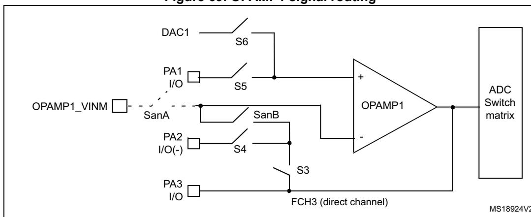
The diagram illustrates the signal routing for OPAMP1. The non-inverting input (+) is connected to a switch S6, which is connected to DAC1, and a switch S5, which is connected to PA1 I/O. The inverting input (-) is connected to a switch SanB, which is connected to PA2 I/O(-) via switch S4, and a switch S3, which is connected to PA3 I/O. A direct channel FCH3 is also connected to the inverting input. The output of OPAMP1 is connected to an ADC Switch matrix. The diagram is labeled MS18924V2.
The routing for the three operational amplifiers can be selected by OPAMP_CSR register.
Analog switches S3 to S6 and SanA can be opened and closed by programming the corresponding OPAMP_CSR register bits independently of whether the amplifiers are enabled or not by the OPA1_PD, OPA2_PD and/or OPA3_PD bits.
Analog switch SanB automatically follows the selection of the S3 or S4 switches. It is not controlled individually.
For OPAMP1, S6 is used to connect DAC_Channel1 to its positive input.
For OPAMP2, there is an additional S7 switch in parallel with S6 in order to select the positive input source as either I/O or DAC_Channel1 or DAC_Channel2.
For OPAMP3, S6 is used to connect DAC_Channel2 to its positive input.
All operational amplifiers can be powered down by setting the OPAx_PD bit. The corresponding inputs and outputs are then in high impedance.
Figure 70. OPAMP2 signal routing
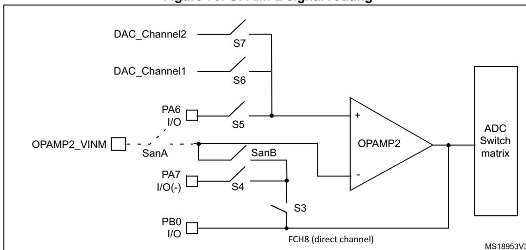
The diagram illustrates the signal routing for OPAMP2. The non-inverting input (+) is connected to a switch S7, which is connected to DAC_Channel2, a switch S6, which is connected to DAC_Channel1, and a switch S5, which is connected to PA6 I/O. The inverting input (-) is connected to a switch SanB, which is connected to PA7 I/O(-) via switch S4, and a switch S3, which is connected to PB0 I/O. A direct channel FCH8 is also connected to the inverting input. The output of OPAMP2 is connected to an ADC Switch matrix. The diagram is labeled MS18953V3.
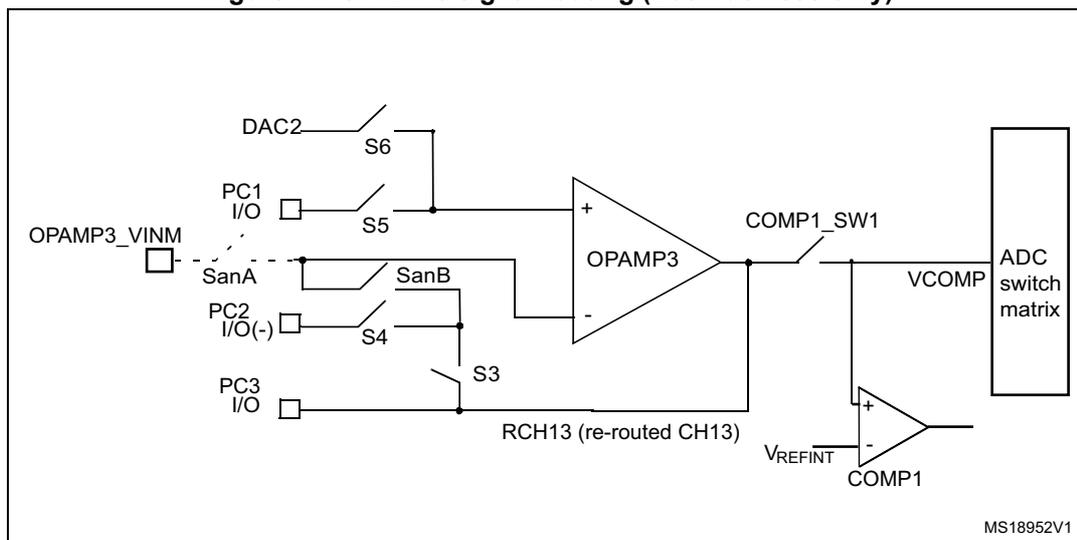
Figure 71. OPAMP3 signal routing (Cat.4 devices only)
15.3.2 Using the OPAMP outputs as ADC inputs
In order to use OPAMP outputs as ADC inputs, the operational amplifiers must be enabled and the ADC must use the OPAMP output channel number. (OPA1: CH3 ; OPA2: CH8 ; OPA3: CH13).
In addition for OPA3 or FCH13, the user must close COMP1_SW1 analog switch to do an acquisition (refer to Section 14.9.1: COMP comparator control and status register (COMP_CSR) on page 340 ).
15.3.3 Calibration
At startup, the trimming values are initialized with the preset 'factory' trimming value.
Furthermore each operational amplifier offset can be trimmed by the user. All switches related to the inputs of each operational amplifier must be open during the trimming operation (SanA, S3, S4, S5, S6).
There are two registers for trimming the offsets of the 3 operational amplifiers for normal mode and low-power mode. Two words of 30-bits, one for standard mode and the other for low-power mode are available in OPAMP_OTR and OPAMP_LPOTR registers. This is the 'user' value.
The user is able to switch from 'factory' values to 'user' trimmed values using the OT_USER bit in the OPAMP_OTR register. This bit is reset at startup to send 'factory' value to the OPAMPs. It is common to the 3 OPAMPs.
The offset of each operational amplifier can be trimmed by programming the OPAMP offset trimming register for normal mode (OPAMP_OTR) . The trimming values are stored in non-volatile memory.
The offset trimming register can be written, typically after a calibration operation initialized by the OPAx_CAL bits.
- • Setting the OPAxCAL_L bit initializes offset calibration for the P differential pair (low voltage reference used).
- • Setting the OPAxCAL_H bit initializes offset calibration for the N differential pair (high voltage reference used).
The 30 useful bits of OPA_OTR or OPA_LP_OTR are composed of three 10-bit words one for each operational amplifier. Each 10-bit is composed of 2 calibration values, the 5 lower bits are for trimming the offset of the PMOS differential pair. The 5 upper bits are for the NMOS ones.
After offset calibration is initialized by setting the control bit as shown in Table 72 , write the new trimming values in the OPAMP offset trimming register for normal mode (OPAMP_OTR) register value until the OPAxCALOUT flag toggles to indicate that the calibration has successfully completed.
Table 72. Operating modes and calibration
| Mode | Control bits | Output | ||||
|---|---|---|---|---|---|---|
| OPAxPD | OPAxLPM | OPAxCAL_H | OPAxCAL_L | V OUT | CALout flag | |
| Normal operating mode | 0 | 0 | 0 | 0 | analog | 0 |
| 1 | 1 | |||||
| Low-power mode | 0 | 1 | 0 | 0 | analog | 0 |
| 1 | 1 | |||||
| Power down | 1 | X | X | X | Z | 0 |
| Offset cal high | 0 | X | 1 | 0 | analog | X |
| Offset cal low | 0 | X | 0 | 1 | analog | X |
Calibration procedure
Follow these steps to perform a full calibration of either one of the operational amplifiers:
- 1. Program the OPAMP_CSR register to open all the switches connected to the operational amplifier.
- 2. Set the OT_USER bit in the OPAMP_OTR register to 1.
- 3. Choose a calibration mode (refer to
Table 72: Operating modes and calibration
). You can begin with:
- • Normal mode, offset cal high
- 4. The code in OPAMP_OTR[OPAxOPT_OFFSET_TRIM_High] is incremented from 00000b to the first value code that causes the OPAxCALOUT output level to change from 0 to 1.
Note: Between the write to the OPAMP_OTR register and the read of the OPAxCALOUT value, take care to wait for the \( t_{OFFTRIMmax} \) delay specified in the datasheet electrical characteristics section, to get the correct OPAxCALOUT value.
The commutation means that the offset is correctly compensated and the corresponding trim code must kept in the OPAMP_OTR register.
The value 11111b is forbidden for OPAMP_OTR[OPAxOPT_OFFSET_TRIM_High].
Repeat steps 3 to 4 for:
- • Normal_mode and offset cal low
- • Low-power mode and offset cal high
- • Low-power mode and offset cal low
If a mode is not used its calibration serves no purpose.
Note: During the whole calibration phase the external connection of the operational amplifier output must not pull up or down currents higher than 500 \( \mu \) A.
15.4 OPAMP registers
15.4.1 OPAMP control/status register (OPAMP_CSR)
Address offset: 0x00
Reset value: 0x0001 0101
| 31 | 30 | 29 | 28 | 27 | 26 | 25 | 24 | 23 | 22 | 21 | 20 | 19 | 18 | 17 | 16 |
|---|---|---|---|---|---|---|---|---|---|---|---|---|---|---|---|
| OPA3C ALOUT | OPA2C ALOUT | OPA1C ALOUT | OPA_R ANGE | S7SEL 2 | ANAW SEL3 | ANAWS EL2 | ANAWS EL1 | OPA3L PM | OPA3C AL_H | OPA3C AL_L | S6SEL 3 | S5SEL 3 | S4SEL 3 | S3SEL 3 | OPA3P D |
| r | r | r | rw | rw | rw | rw | rw | rw | rw | rw | rw | rw | rw | rw | |
| 15 | 14 | 13 | 12 | 11 | 10 | 9 | 8 | 7 | 6 | 5 | 4 | 3 | 2 | 1 | 0 |
| OPA2L PM | OPA2C AL_H | OPA2C AL_L | S6SEL 2 | S5SEL 2 | S4SEL 2 | S3SEL 2 | OPA2P D | OPA1L PM | OPA1C AL_H | OPA1C AL_L | S6SEL 1 | S5SEL 1 | S4SEL 1 | S3SEL 1 | OPA1P D |
| rw | rw | rw | rw | rw | rw | rw | rw | rw | rw | rw | rw | rw | rw | rw | rw |
- Bit 31
OPA3CALOUT
: OPAMP3 calibration output
During calibration mode, the offset is trimmed when this signal toggles. - Bit 30
OPA2CALOUT
: OPAMP2 calibration output
During calibration mode, the offset is trimmed when this signal toggles. - Bit 29
OPA1CALOUT
: OPAMP1 calibration output
During calibration mode, the offset is trimmed when this signal toggles. - Bit 28
OPA_RANGE
: Power range selection
This bit can be set and cleared by software when the operational amplifiers are in powered down. It select the operational amplifier power supply range for stability.
0: Low range ( \( V_{DDA} < 2.4\text{ V} \) )
1: High range ( \( V_{DDA} > 2.4\text{ V} \) ) - Bit 27
S7SEL2
: Switch 7 for OPAMP2 enable
0: S7 opened
1: S7 closed - Bit 26
ANAWSEL3
: Switch SanA enable for OPAMP3
0: SanA switch opened
1: SanA switch closed - Bit 25
ANAWSEL2
: Switch SanA enable for OPAMP2
0: SanA switch opened
1: SanA switch closed - Bit 24
ANAWSEL1
: Switch SanA enable for OPAMP1
0: SanA switch opened
1: SanA switch closed - Bit 23
OPA3LPM
: OPAMP3 low-power mode
0: OPAMP3 low-power mode off
1: OPAMP3 low-power mode on - Bit 22
OPA3CAL_H
: OPAMP3 offset calibration for N differential pair
0: OPAMP3 offset calibration for N diff OFF
1: OPAMP3 offset calibration for N diff ON if OPA3CAL_L = 0 - Bit 21
OPA3CAL_L
: OPAMP3 offset Calibration for P differential pair
0: OPAMP3 offset calibration for P diff OFF
1: OPAMP3 offset calibration for P diff ON if OPA3CAL_H = 0 - Bit 20
S6SEL3
: Switch 6 for OPAMP3 enable
0: S6 switch opened
1: S6 switch closed - Bit 19
S5SEL3
: Switch 5 for OPAMP3 enable
0: S5 switch opened
1: S5 switch closed - Bit 18
S4SEL3
: Switch 4 for OPAMP3 enable
0: S4 switch opened
1: S4 switch closed - Bit 17
S3SEL3
: Switch 3 for OPAMP3 Enable
0: S3 switch opened
1: S3 switch closed
- Bit 16
OPA3PD
: OPAMP3 power down
0: OPAMP3 enabled
1: OPAMP3 disabled - Bit 15
OPA2LPM
: OPAMP2 low-power mode
0: OPAMP2 low-power mode off
1: OPAMP2 low-power mode on - Bit 14
OPA2CAL_H
: OPAMP2 offset calibration for N differential pair
0: OPAMP2 offset calibration for N diff OFF
1: OPAMP2 offset calibration for N diff ON if OPA2CAL_L = 0 - Bit 13
OPA2CAL_L
: OPAMP2 offset Calibration for P differential pair
0: OPAMP2 offset calibration for P diff OFF
1: OPAMP2 offset calibration for P diff ON if OPA2CAL_H = 0 - Bit 12
S6SEL2
: Switch 6 for OPAMP2 enable
0: S6 switch opened
1: S6 switch closed - Bit 11
S5SEL2
: Switch 5 for OPAMP2 enable
0: S5 switch opened
1: S5 switch closed - Bit 10
S4SEL2
: Switch 4 for OPAMP2 enable
0: S4 switch opened
1: S4 switch closed - Bit 9
S3SEL2
: Switch 3 for OPAMP2 enable
0: S3 switch opened
1: S3 switch closed - Bit 8
OPA2PD
: OPAMP2 power down
0: OPAMP2 enabled
1: OPAMP2 disabled - Bit 7
OPA1LPM
: OPAMP1 low-power mode
0: OPAMP1 low-power mode off
1: OPAMP1 in low-power mode on - Bit 6
OPA1CAL_H
: OPAMP1 offset calibration for N differential pair
0: OPAMP1 offset calibration for N diff OFF
1: OPAMP1 offset calibration for N diff ON if OPA1CAL_L = 0 - Bit 5
OPA1CAL_L
: OPAMP1 offset calibration for P differential pair
0: OPAMP1 offset calibration for P diff OFF
1: OPAMP1 offset calibration for P diff ON if OPA1CAL_H = 0 - Bit 4
S6SEL1
: Switch 6 for OPAMP1 enable
0: S6 switch opened
1: S6 switch closed - Bit 3
S5SEL1
: Switch 5 for OPAMP1 enable
0: S5 switch opened
1: S5 switch closed
Bit 2
S4SEL1
: Switch 4 for OPAMP1 enable
0: S4 switch opened
1: S4 switch closed
Bit 1
S3SEL1
: Switch 3 for OPAMP1 enable
0: S3 switch opened
1: S3 switch closed
Bit 0
OPA1PD
: OPAMP1 power down
0: OPAMP1 enabled
1: OPAMP1 disabled
15.4.2 OPAMP offset trimming register for normal mode (OPAMP_OTR)
Address offset: 0x04
Bit 31 reset value: 0
Bits 29:0 reset value: Factory trimmed value is restored.
| 31 | 30 | 29 | 28 | 27 | 26 | 25 | 24 | 23 | 22 | 21 | 20 | 19 | 18 | 17 | 16 |
|---|---|---|---|---|---|---|---|---|---|---|---|---|---|---|---|
| OT_ USER | Res. | OA3_OPT_OFFSET_TRIM_HIGH | OA3_OPT_OFFSET_TRIM_LOW | OA2_OPT_OFFSET_TRIM_HIGH[4:1] | |||||||||||
| w | rw | rw | rw | rw | rw | rw | rw | rw | rw | rw | rw | rw | rw | rw | |
| 15 | 14 | 13 | 12 | 11 | 10 | 9 | 8 | 7 | 6 | 5 | 4 | 3 | 2 | 1 | 0 |
| OA2_OPT_OFFSET_TRIM_HIGH[0] | OA2_OPT_OFFSET_TRIM_LOW | OA1_OPT_OFFSET_TRIM_HIGH | OA1_OPT_OFFSET_TRIM_LOW | ||||||||||||
| rw | rw | rw | rw | rw | rw | rw | rw | rw | rw | rw | rw | rw | rw | rw | rw |
Bit 31
OT_USER
Select user or factory trimming value
This bit is set and cleared by software, it is always read as 0. It is used to select if the OPAMPx offset is trimmed by the preset factory-programmed trimming values or the user programmed trimming value.
0: Trim the OPAMP offset using default factory values
1: Trim the OPAMP offset using user programmed values
Bit 30 Reserved, must be kept at reset value
- Bit 29:25 OA3_OPT_OFFSET_TRIM_HIGH[4:0] : OPAMP3, normal mode 5-bit offset trim value for NMOS pairs
- Bit 24:20 OA3_OPT_OFFSET_TRIM_LOW[4:0] : OPAMP3, normal mode 5-bit offset trim value for PMOS pairs
- Bit 19:15 OA2_OPT_OFFSET_TRIM_HIGH[4:0] : OPAMP2, normal mode 5-bit offset trim value for NMOS pairs
- Bit 14:10 OA2_OPT_OFFSET_TRIM_LOW[4:0] : OPAMP2, normal mode 5-bit offset trim value for PMOS pairs
- Bit 9:5 OA1_OPT_OFFSET_TRIM_HIGH[4:0] : OPAMP1, normal mode 5-bit offset trim value for NMOS pairs
- Bit 4:0 OA1_OPT_OFFSET_TRIM_LOW[4:0] : OPAMP1, normal mode 5-bit offset trim value for PMOS pairs
15.4.3 OPAMP offset trimming register for low-power mode (OPAMP_LPOTR)
Address offset: 0x08
Bits 29:0 reset value: Factory trimmed value is restored.
| 31 | 30 | 29 | 28 | 27 | 26 | 25 | 24 | 23 | 22 | 21 | 20 | 19 | 18 | 17 | 16 |
|---|---|---|---|---|---|---|---|---|---|---|---|---|---|---|---|
| Reserved | OA3_OPT_OFFSET_TRIM_LP_HIGH | OA3_OPT_OFFSET_TRIM_LP_LOW | OA2_OPT_OFFSET_TRIM_LP_HIGH[4:1] | ||||||||||||
| rw | rw | rw | rw | rw | rw | rw | rw | rw | rw | rw | rw | rw | rw | rw | |
| 15 | 14 | 13 | 12 | 11 | 10 | 9 | 8 | 7 | 6 | 5 | 4 | 3 | 2 | 1 | 0 |
| OA2_OPT_OFFSET_TRIM_LP_HIGH | OA2_OPT_OFFSET_TRIM_LP_LOW | OA1_OPT_OFFSET_TRIM_LP_HIGH | OA1_OPT_OFFSET_TRIM_LP_LOW | ||||||||||||
| rw | rw | rw | rw | rw | rw | rw | rw | rw | rw | rw | rw | rw | rw | rw | |
Bits 31:30 Reserved, must be kept at reset value
Bit 29:25 OA3_OPT_OFFSET_TRIM_LP_HIGH[4:0] : OPAMP3, low-power mode 5-bit offset trim value for NMOS pairs
Bit 24:20 OA3_OPT_OFFSET_TRIM_LP_LOW[4:0] : OPAMP3, low-power mode 5-bit offset trim value for PMOS pairs
Bit 19:15 OA2_OPT_OFFSET_TRIM_LP_HIGH[4:0] : OPAMP2, low-power mode 5-bit offset trim value for NMOS pairs
Bit 14:10 OA2_OPT_OFFSET_TRIM_LP_LOW[4:0] : OPAMP2, low-power mode 5-bit offset trim value for PMOS pairs
Bit 9:5 OA1_OPT_OFFSET_TRIM_LP_HIGH[4:0] : OPAMP1, low-power mode 5-bit offset trim value for NMOS pairs
Bit 4:0 OA1_OPT_OFFSET_TRIM_LP_LOW[4:0] : OPAMP1, low-power mode 5-bit offset trim value for PMOS pairs
15.4.4 OPAMP register map
Table 73. OPAMP register map
| Offset | Register name | 31 | 30 | 29 | 28 | 27 | 26 | 25 | 24 | 23 | 22 | 21 | 20 | 19 | 18 | 17 | 16 | 15 | 14 | 13 | 12 | 11 | 10 | 9 | 8 | 7 | 6 | 5 | 4 | 3 | 2 | 1 | 0 |
|---|---|---|---|---|---|---|---|---|---|---|---|---|---|---|---|---|---|---|---|---|---|---|---|---|---|---|---|---|---|---|---|---|---|
| OPA3CALOUT | OPA2CALOUT | OPA1CALOUT | OPA_RANGE | S7SEL2 | ANAWSEL3 | ANAWSEL2 | ANAWSEL1 | OPA3LPM | OPA3CAL_H | OPA3CAL_L | S6SEL3 | S5SEL3 | S4SEL3 | S3SEL3 | OPA3PD | OPA2LPM | OPA2CAL_H | OPA2CAL_L | S6SEL2 | S5SEL2 | S4SEL2 | S3SEL2 | OPA2PD | OPA1LPM | OPA1CAL_H | OPA1CAL_L | S6SEL1 | S5SEL1 | S4SEL1 | S3SEL1 | OPA1PD | ||
| 0x00 | OPAMP_CSR_ | ||||||||||||||||||||||||||||||||
| 0x04 | OPAMP_OTR_ | OT_USER | Reserved | OA3_OPT_OFFSET_TRIM_HIGH | OA3_OPT_OFFSET_TRIM_LOW | OA2_OPT_OFFSET_TRIM_HIGH | OA2_OPT_OFFSET_TRIM_LOW | OA1_OPT_OFFSET_TRIM_HIGH | OA1_OPT_OFFSET_TRIM_LOW | ||||||||||||||||||||||||
| 0x08 | OPAMP_LPOTR_ | Reserved | OA3_OPT_OFFSET_TRIM_LP_HIGH | OA3_OPT_OFFSET_TRIM_LP_LOW | OA2_OPT_OFFSET_TRIM_LP_HIGH | OA2_OPT_OFFSET_TRIM_LP_LOW | OA1_OPT_OFFSET_TRIM_LP_HIGH | OA1_OPT_OFFSET_TRIM_LP_LOW | |||||||||||||||||||||||||
Refer to Table 5 on page 47 for the Register boundary addresses table.