14. Comparators (COMP)
This section applies to the whole STM32L1xxxx family, unless otherwise specified.
14.1 Introduction
The STM32L1xxxx contains two zero-crossing comparators COMP1 and COMP2, that share the same current bias.
Note: For all I/Os used as comparator inputs, the GPIO registers must be configured in analog mode.
When using the routing interface (see Section 8: System configuration controller (SYSCFG) and routing interface (RI) ), the comparator inputs can be connected to external I/Os.
14.2 Main features
- • A comparator (COMP1) with fixed threshold (internal reference voltage). The non-inverting input can be selected among 24 external I/Os.
- • A rail-to-rail comparator (COMP2) with selectable threshold. The non-inverting input can be selected among 2 I/Os for Cat.1 and Cat.2 devices or among 4 I/Os for Cat.3, Cat.4, Cat.5 and Cat.6 devices. The inverting input can be selected among 7 inputs:
- – the internal reference voltage ( \( V_{REFINT} \) )
- – an internal reference voltage submultiple (1/4, 1/2, 3/4) provided by buffered \( V_{REFINT} \) divider.
- – the DAC1 output
- – the DAC2 output
- – an external I/O (PB3)
- • The 2 comparators can be combined to form window comparators.
- • Zero-crossing can generate a rising or falling edge on the comparator outputs depending on the trigger configuration.
- • Each comparator has an interrupt generation capability with wakeup from the Sleep and Stop.
- • The COMP2 output can be redirected to TIM2/TIM3/TIM4’s input capture 4 (IC4) or OCREF_CLR inputs, or to the TIM10s input capture 1 (IC1).
- • COMP2 speed is configurable for optimum speed/consumption ratio.
The complete block diagram of the comparators, routing interface and ADC interface is shown in section Section 8: System configuration controller (SYSCFG) and routing interface (RI) .
14.3 COMP clock
The COMP clock provided by the clock controller is synchronous with the PCLK1 (APB1 clock).
14.4 Comparator 1 (COMP1)
Figure 63 and Figure 64 show the comparator 1 interconnections.
Figure 63. COMP1 interconnections (Cat.1 and Cat.2 devices)
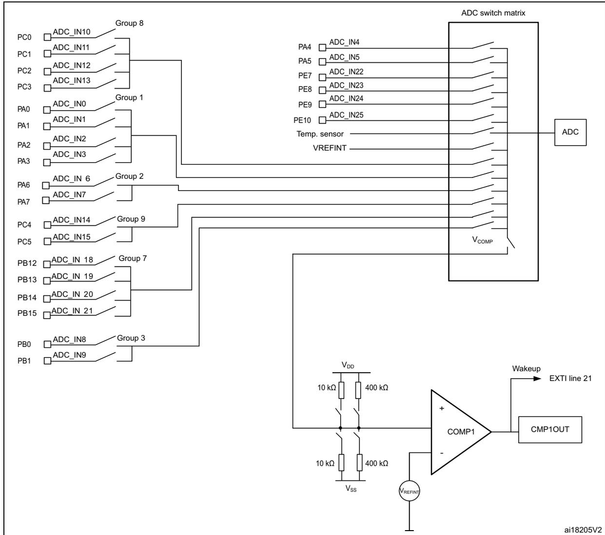
The diagram illustrates the internal architecture and interconnections of the COMP1 comparator. On the left, various pins are listed with their corresponding ADC input names, grouped into several categories:
- Group 8: PC0 (ADC_IN10), PC1 (ADC_IN11), PC2 (ADC_IN12), PC3 (ADC_IN13).
- Group 1: PA0 (ADC_IN0), PA1 (ADC_IN1), PA2 (ADC_IN2), PA3 (ADC_IN3).
- Group 2: PA6 (ADC_IN6), PA7 (ADC_IN7).
- Group 9: PC4 (ADC_IN14), PC5 (ADC_IN15).
- Group 7: PB12 (ADC_IN18), PB13 (ADC_IN19), PB14 (ADC_IN20), PB15 (ADC_IN21).
- Group 3: PB0 (ADC_IN8), PB1 (ADC_IN9).
Note: The internal reference voltage and temperature sensor cannot be used as COMP1 non-inverting input.
COMP1 comparator and ADC cannot be used at the same time since they share the ADC switch matrix.
Figure 64. COMP1 interconnections (Cat.3, Cat.4, Cat.5 and Cat.6 devices)
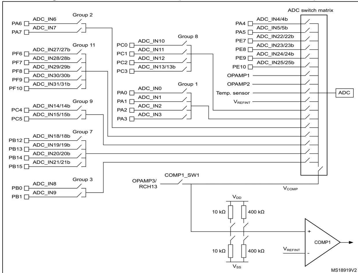
Note: The internal reference voltage and temperature sensor cannot be used as COMP1 non-inverting input.
COMP1 comparator and ADC cannot be used at the same time since they share the ADC switch matrix.
To use the COMP1 comparator, the application has to perform the following steps:
- 1. Enable the comparator 1 by setting the CMP1EN bit in the COMP_CSR register
- 2. Wait until the comparator is ready (when the startup time has elapsed). Refer to the electrical characteristics of the STM32L1xxxx datasheet.
- 3. Set the SCM bit in the RI_ASCR1 register so as to close the ADC switches if the corresponding I/O switch is also closed
- 4. Close the ADC switches to create the path from the selected I/O to the non-inverting input. The input can be any of the up to 29 available I/Os and can be split into groups or not (see
Figure 41: I/O groups and selection on page 196
):
- a) Close the VCOMP ADC analog switch by setting the VCOMP bit in the RI_ASCR1 register.
- b) Close the I/O analog switch number n corresponding to the I/O group that must be connected to the COMP1 non-inverting input, by setting the CHn bit in RI_ASCR1.
- 5. If required enable the COMP1 interrupt by configuring and enabling EXTI line21 in interrupt mode and selecting the desired trigger event (rising edge, falling edge or both).
14.5 Comparator 2 (COMP2)
Figure 65 and Figure 66 show the comparator 2 interconnections.
Figure 65. COMP2 interconnections (Cat.1 and Cat.2 devices)
![Figure 65: COMP2 interconnections (Cat.1 and Cat.2 devices). This diagram shows the internal architecture of the COMP2 comparator. The non-inverting input (+) is connected to Group 6 (PB4/GR6-1 and PB5/GR6-2) and Vss. The inverting input (-) is connected to PB3 (I/O port), DAC_OUT1, DAC_OUT2, and a VREFINT divider providing 1/4, 1/2, 3/4, and ~1.2V. The output is connected to CMP2OUT, which can be routed to EXTI line 22 (Wakeup) or selected via OUTSEL[2:0] bits to TIM2 input capture 4, TIM2 OCREF clear, TIM3 input capture 4, TIM3 OCREF clear, TIM4 input capture 4, TIM4 OCREF clear, or TIM10 input capture 1.](/RM0038-STM32L100-151-152-162/ad794501076b4a6016598132749175e5_img.jpg)
Figure 66. COMP2 interconnections (Cat.3, Cat.4, Cat.5 and Cat.6 devices)
![Figure 66: COMP2 interconnections (Cat.3, Cat.4, Cat.5 and Cat.6 devices). This diagram is similar to Figure 65 but includes additional I/O options for Group 6: PB6/GR6-3 and PB7/GR6-4. The rest of the architecture, including the VREFINT divider, DAC inputs, and output routing options (EXTI line 22, CMP2OUT, and TIM inputs via OUTSEL[2:0] bits), remains the same.](/RM0038-STM32L100-151-152-162/212f85622719de88fe92d2a398eb778f_img.jpg)
To use the COMP2 comparator, the application has to perform the following steps:
- 1. Select COMP2's inverting input with the INSEL[2:0] bits in COMP_CSR.
- – In the case of an external I/O selection (PB3 I/O), the I/O should be configured in analog input mode.
- 2. Close the I/O's analog switch to connect to COMP2 non-inverting input. The input can be any I/O in group 6 (see Table 41: I/O groups and selection on page 196 ). GR6-1 or
GR6-2 switches are closed as soon as the corresponding I/O is configured in analog mode.
- 3. Wait until the comparator is ready (when the startup time has elapsed). Refer to the electrical characteristics of the STM32L1xxxx datasheet.
- 4. If required, perform the following procedures:
- – Select the speed with the SPEED bit in COMP_CSR.
- – Redirect the COMP2 output to TIM2, TIM3, TIM4 or TIM10 by configuring the OUTSEL[2:0] bits in COMP_CSR (refer to Figure 67 ).
- – Enable the COMP2 interrupt by configuring and enabling EXTI line22 in interrupt mode and selecting the desired sensitivity level.
Note: GR6-1 and GR6-2 I/O switches can be closed by either configuring the corresponding I/O (PB4 or PB5) in analog mode (Schmitt trigger disabled) or configuring the I/O in input floating mode and setting GR6-1 or GR6-2 in RI_ASCR2 (Schmitt trigger enabled). If PB4 or PB5 is used as comparator input, it is recommended to use analog configuration to avoid any overconsumption around \( V_{DD}/2 \) .
Note: The COMP2 comparator is enabled as soon as the inverting input is selected. The channel can be changed when the comparator is enabled.
The following figure shows the output redirection possibilities of the COMP2 output.
Figure 67. Redirecting the COMP2 output
![Diagram illustrating the output redirection possibilities of the COMP2 output. The COMP2 comparator output (CMP2OUT) is connected to a multiplexer controlled by the OUTSEL[2:0] bits. The output can be redirected to various internal signals: TIM2 input capture 4, TIM2 OCREP clear, TIM3 input capture 4, TIM3 OCREP clear, TIM4 input capture 4, TIM4 OCREP clear, or TIM10 input capture 1. The output is also connected to the EXTI line 22 for wakeup purposes.](/RM0038-STM32L100-151-152-162/a32e424673c378ae154466f388217f40_img.jpg)
The diagram shows a comparator labeled 'COMP2' with '+' and '-' inputs. Its output is labeled 'CMP2OUT'. This output is connected to a multiplexer. The multiplexer is controlled by 'OUTSEL[2:0] bits'. The output of the multiplexer is connected to a list of internal signals: 'TIM2 input capture 4', 'TIM2 OCREP clear', 'TIM3 input capture 4', 'TIM3 OCREP clear', 'TIM4 input capture 4', 'TIM4 OCREP clear', and 'TIM10 input capture 1'. Additionally, the 'CMP2OUT' signal is connected to 'EXTI line 22', which is labeled 'Wakeup'.
Note: For more details about “clearing TIMx OCREP”, refer to Section 17.3.11: Clearing the OCxREF signal on an external event on page 407 .
14.6 Comparators in Window mode
Figure 68. Comparators in Window mode
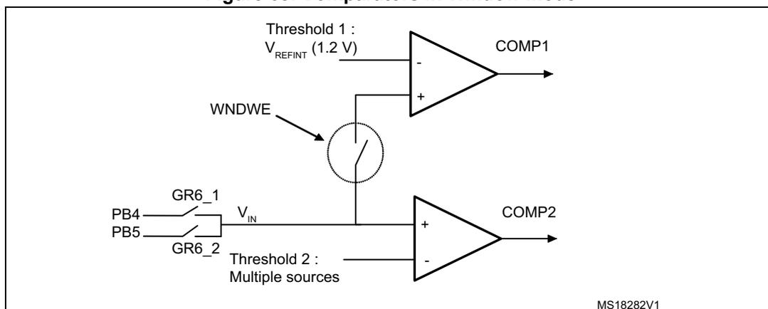
To use the COMP1 and COMP2 comparators in window mode, the application has to perform the following steps:
- 1. Enable the Window mode by setting WNDWE in the COMP_CSR register.
- 2. Configure the comparators:
- – for COMP1: enable the comparator: follow the steps 1 and 2 from Section 14.4: Comparator 1 (COMP1)
- – for COMP2: enable the comparator, select inverting and non-inverting inputs: follow steps 1, 2, 3 and 4 from Section 14.5: Comparator 2 (COMP2) .
Note: In Window mode, only the Group 6 (PB4 and PB5 for Cat.1 and Cat.2 devices, PB4, PB5, PB6, PB7 for Cat.3, Cat.4, Cat.5 and Cat.6 devices) can be used as a non-inverting input.
14.7 Low-power modes
Table 70. Comparator behavior in the low-power modes
| Mode | Description |
|---|---|
| Sleep | No effect on the comparators. Comparator interrupts cause the device to exit the Sleep mode. |
| Stop | No effect on the comparators. Comparator interrupts cause the device to exit the Stop mode. |
Note: Comparators cannot be used to exit the device from Sleep or Stop mode when the internal reference voltage is switched off using the ULP bit in the PWR_CR register.
14.8 Interrupts
The comparator interrupts are connected to EXTI controller (lines 21 and 22).
To enable the COMP interrupt, the following sequence is required:
- 1. Configure and enable the EXTI line 21 (COMP1) or EXTI line 22 (COMP2) in interrupt mode and select the desired trigger event (rising edge, falling edge, or both),
- 2. Configure and enable the COMP_IRQ channel in the NVIC.
14.9 COMP registers
The peripheral registers have to be accessed by words (32-bit).
14.9.1 COMP comparator control and status register (COMP_CSR)
The COMP_CSR register is the control/status register of the comparators. It contains all the bits related to both comparators.
Address offset: 0x00
Reset value: 0x0000 0000
| 31 | 30 | 29 | 28 | 27 | 26 | 25 | 24 | 23 | 22 | 21 | 20 | 19 | 18 | 17 | 16 |
|---|---|---|---|---|---|---|---|---|---|---|---|---|---|---|---|
| TSUSP | CAIF | CAIE | RCH13 | FCH8 | FCH3 | Reserved | OUTSEL[2:0] | INSEL[2:0] | WNDWE | VREFOU TEN | |||||
| rw | r | rw | rw | rw | rw | rw | rw | rw | rw | rw | rw | rw | rw | ||
| 15 | 14 | 13 | 12 | 11 | 10 | 9 | 8 | 7 | 6 | 5 | 4 | 3 | 2 | 1 | 0 |
|---|---|---|---|---|---|---|---|---|---|---|---|---|---|---|---|
| Reserved | CMP2OUT | SPEED | Reserved | CMP1OUT | Res. | COMP1_SW1 | CMP1_EN | 400KPD | 10KPD | 400KPU | 10KPU | ||||
| r | rw | r | rw | rw | rw | rw | rw | rw | |||||||
Bit 31 TSUSP : Suspend Timer Mode
0: TIM9 ITR enabled to suspend OC TIM9 generation
1: TIM9 ITR not used to suspend OC TIM9 generation
Note: This bit is available in Cat.3, Cat.4, Cat.5 and Cat.6 devices only
Bit 30 CAIF : Channel acquisition interrupt flag
0: Channel acquisition ongoing or not started
1: Channel acquisition completed
Note: This bit is available in Cat.3, Cat.4, Cat.5 and Cat.6 devices only
Bit 29 CAIE : Channel Acquisition Interrupt Enable / Clear
This bit is set and cleared to enable the Channel Acquisition interrupt. When the Caif bit is set, it must be cleared by writing 0 to the CAIE bit.
0: Channel acquisition interrupt disabled
1: Channel acquisition interrupt enabled
This bit is available in Cat.3, Cat.4, Cat.5 and Cat.6 devices only
Bit 28 RCH13 : Select GPIO port PC3 as re-routed ADC input channel CH13.
This bit is set and cleared by software in order configure PC3 to be used as re-routed channel CH13 (selected by the ADC interface) if OPAMP3 is in power down mode (OPA3PD bit = 0 in OPAMP_CSR register (Cat.4 devices only). See Figure 71: OPAMP3 signal routing (Cat.4 devices only) on page 346 .
0: PC3 can be used as slow ADC channel
1: PC3 can be used as re-routed ADC channel
Note: This bit is available in Cat.4 devices only
Bit 27 FCH8 : Select GPIO port PB0 as fast ADC input channel CH8.
This bit is set and cleared by software in order configure PB0 to be used as direct channel CH8 (selected by the ADC interface) if OPAMP2 is in power down mode (OPA2PD bit = 0 in OPAMP_CSR register. See Figure 70: OPAMP2 signal routing on page 345 .
0: PB0 can be used as slow ADC channel
1: PB0 can be used as fast ADC channel
Note: This bit is available in Cat.3, Cat.4, Cat.5 and Cat.6 devices only
Bit 26 FCH3 : Select GPIO port PA3 as fast ADC input channel CH3.
This bit is set and cleared by software in order configure PA3 to be used as direct channel CH3 (selected by the ADC interface) if OPAMP1 is in power down mode (OPA1PD bit = 0 in OPAMP_CSR register. See Figure 69: OPAMP1 signal routing on page 345 .
0: PA3 can be used as slow ADC channel
1: PA3 can be used as fast ADC channel
Note: This bit is available in Cat.3, Cat.4, Cat.5 and Cat.6 devices only
Bits 25:24 Reserved, must be kept cleared.
Bits 23:21 OUTSEL : Comparator 2 output selection
These bits are written by software to connect the output of COMP2 to a selected timer input.
000 = TIM2 Input Capture 4
001 = TIM2 OCREF_CLR
010 = TIM3 Input Capture 4
011 = TIM3 OCREF_CLR
100 = TIM4 Input Capture 4
101 = TIM4 OCREF_CLR
110 = TIM10 Input Capture 1
111 = no redirection
Bits 20:18 INSEL : Inverted input selection
000 = no selection
001 = External I/O: PB3 (COMP2_INM)
010 =
\(
V_{REFINT}
\)
011 =
\(
3/4 V_{REFINT}
\)
100 =
\(
1/2 V_{REFINT}
\)
101 =
\(
1/4 V_{REFINT}
\)
110 = DAC_OUT1
111 = DAC_OUT2
Note: The COMP2 comparator is enabled when the INSEL bit values are different from "000".
Bit 17 WNDWE : Window mode enable
0: Disabled
1: Enabled
Bit 16 VREFOUTEN : V REFINT output enable
This bit is used to output V REFINT on Group 3 (refer to Figure 28: Internal reference voltage output ).
0: Disabled
1: Enabled
Bits 15:14 Reserved, must be kept at reset value
Bit 13 CMP2OUT : Comparator 2 output
This bit indicates the low or high level of the comparator 2 output.
0: Comparator 2 output is low when the non-inverting input is at a lower voltage than the inverting input
1: Comparator 2 output is high when the non-inverting input is at a higher voltage than the inverting input
Bit 12 SPEED : Comparator 2 speed mode
0: slow speed
1: fast speed
Bits 11:8 Reserved, must be kept at reset value
Bit 7 CMP1OUT : Comparator 1 output
This bit indicates the high or low level of the comparator 1 output.
0: Comparator 1 output is low when the non-inverting input is at a lower voltage than the inverting input
1: Comparator 1 output is high when the non-inverting input is at a higher voltage than the inverting input
Bit 6 Reserved, must be kept at reset value
Bit 5 SW1 : COMP1_SW1 analog switch enable
This bit is set and cleared by software to control the COMP1_SW1 analog switch in order to redirect OPAMP3 output or PC3 to the ADC switch matrix and/or the positive input of COMP1.
0: COMP1_SW1 analog switch open
1: COMP1_SW1 analog switch closed
Note: This bit is available in Cat.4 devices only
Bit 4 CMP1EN : Comparator 1 enable
0: Comparator 1 disabled
1: Comparator 1 enabled
Bit 3 400KPD : 400 k \( \Omega \) pull-down resistor
This bit enables the 400 k \( \Omega \) pull-down resistor.
0: 400 k \( \Omega \) pull-down resistor disabled
1: 400 k \( \Omega \) pull-down resistor enabled
- Bit 2
10KPD
: 10 k
\(
\Omega
\)
pull-down resistor
This bit enables the 10 k \( \Omega \) pull-down resistor.
0: 10 k \( \Omega \) pull-down resistor disabled
1: 10 k \( \Omega \) pull-down resistor enabled - Bit 1
400KPU
: 400 k
\(
\Omega
\)
pull-up resistor
This bit enables the 400 k \( \Omega \) pull-up resistor.
0: 400 k \( \Omega \) pull-up resistor disabled
1: 400 k \( \Omega \) pull-up resistor enabled - Bit 0
10KPU
: 10 k
\(
\Omega
\)
pull-up resistor
This bit enables the 10 k \( \Omega \) pull-up resistor.
0: 10 k \( \Omega \) pull-up resistor disabled
1: 10 k \( \Omega \) pull-up resistor enabled
Note: To avoid extra power consumption, only one resistor should be enabled at a time.
14.9.2 COMP register map
Table 71: COMP register map and reset values summarizes the COMP registers. The reserved memory areas are highlighted in gray in the table.
Table 71. COMP register map and reset values
| Offset | Register | 31 | 30 | 29 | 28 | 27 | 26 | 25 | 24 | 23 | 22 | 21 | 20 | 19 | 18 | 17 | 16 | 15 | 14 | 13 | 12 | 11 | 10 | 9 | 8 | 7 | 6 | 5 | 4 | 3 | 2 | 1 | 0 | |
|---|---|---|---|---|---|---|---|---|---|---|---|---|---|---|---|---|---|---|---|---|---|---|---|---|---|---|---|---|---|---|---|---|---|---|
| 0x00 | COMP_CSR | TSUSP | CAIF | CAIE | RCH13 | FCH8 | FCH3 | Res. | OUTSEL [2:0] | INSEL [2:0] | WINDWE | VREFOUTEN | Reserved | CMP2OUT | SPEED | Reserved | CMP1OUT | Reserved | COMP1_SW1 | CMP1EN | 400KPD | 10KPD | 400KPU | 10KPU | ||||||||||
| Reset value | 0 | 0 | 0 | 0 | 0 | 0 | 0 | 0 | 0 | 0 | 0 | 0 | 0 | 0 | 0 | 0 | 0 | 0 | 0 | 0 | 0 |
Refer to Table 5 on page 47 for the Register boundary addresses table.