12. Analog-to-digital converter (ADC)
This section applies to the whole STM32L1xxxx family, unless otherwise specified.
12.1 ADC introduction
The 12-bit ADC is a successive approximation analog-to-digital converter. It has up to 42 multiplexed channels allowing it measure signals from up to 40 external and two internal sources. The A/D conversion of the channels can be performed in single, continuous, scan or discontinuous mode. The result of the ADC is stored into a left- or right-aligned 16-bit data register.
The analog watchdog feature allows the application to detect if the input voltage goes beyond the user-defined, higher or lower thresholds.
Conversions are always performed at maximum speed to have the highest possible conversion rate for a given system clock frequency. The automatic power control dramatically reduces the consumption by powering-on the ADC only during conversions.
12.2 ADC main features
- • 12-bit, 10-bit, 8-bit or 6-bit configurable resolution
- • Interrupt generation at the end of regular conversions, end of injected conversions, and in case of analog watchdog or overrun events (for regular conversions)
- • Single and continuous conversion modes
- • Scan mode for automatic conversions in a fully programmable order
- • Programmable data alignment with in-built data coherency
- • Programmable and individual sampling time for each ADC channel
- • External trigger option with configurable edge detection for both regular and injected conversions
- • Discontinuous mode
- • ADC conversion time: 1 µs at full speed (ADC clocked at 16 MHz) down to 4 µs at low speed (ADC clocked at 4 MHz), independent of the APB clock
- • Automatic power-up/power-down to reduce the power consumption
- • ADC supply requirements:
- – 2.4 V to 3.6 V at full speed or with reference zooming ( \( V_{REF+} < V_{DDA} \) )
- – down to 1.8 V at slower speeds
- • ADC input range: \( V_{REF-} \leq V_{IN} \leq V_{REF+} \)
- • Automatic programmable hardware delay insertion between conversions
- • DMA request generation during regular channel conversion
Figure 39 shows the block diagram of the ADC.
Note: \( V_{REF-} \) , if available (depending on package), must be tied to \( V_{SSA} \) .
12.3 ADC functional description
Figure 39 and Figure 40 show the ADC block diagram, Table 58 gives the pin description.
Figure 39. ADC block diagram (Cat.1 and Cat.2 devices)
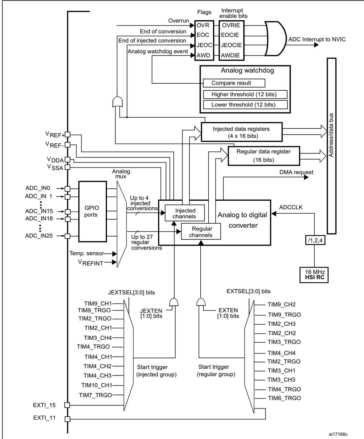
The diagram illustrates the internal architecture of the ADC. On the left, input pins include VREF+, VREF-, VDDA, VSSA, ADC_IN0 through ADC_IN25, a Temp. sensor, and VREFINT. These connect to an 'Analog mux' which feeds into 'GPIO ports'. The 'GPIO ports' output connects to an 'ADC to digital converter' block. This converter has 'Injected channels' (up to 4) and 'Regular channels' (up to 27). Above the converter, an 'Analog watchdog' block contains 'Compare result', 'Higher threshold (12 bits)', and 'Lower threshold (12 bits)'. It receives input from the 'ADC to digital converter' and sends 'Overrun', 'End of conversion', 'End of injected conversion', and 'Analog watchdog event' signals to a 'Flags' register. The 'Flags' register includes OVR, EOC, JEOC, and AWD flags, which are also connected to 'Interrupt enable bits' (OVRIE, EOCIE, JEOCIE, AWDIE). These enable bits are ANDed to generate an 'ADC Interrupt to NVIC'. Below the converter, 'Injected data registers (4 x 16 bits)' and a 'Regular data register (16 bits)' store conversion results and connect to an 'Address/data bus'. A 'DMA request' is generated from the 'Regular data register'. The 'ADC to digital converter' is clocked by 'ADCCLK', which is derived from a '16 MHz HSI RC' oscillator through a divider ('/1,2,4'). At the bottom, 'Start trigger' inputs for injected and regular groups are selected via 'JEXTSEL[3:0] bits' and 'EXTSEL[3:0] bits' respectively. These are ANDed with 'JEXTEN [1:0] bits' and 'EXTEN [1:0] bits' to control the converter. External triggers include TIM9_CH1, TIM9_TRGO, TIM2_TRGO, TIM2_CH1, TIM3_CH4, TIM4_TRGO, TIM4_CH1, TIM4_CH2, TIM4_CH3, TIM10_CH1, TIM7_TRGO, EXTI_15, and EXTI_11 for the injected group; and TIM9_CH2, TIM9_TRGO, TIM2_CH3, TIM2_CH2, TIM3_TRGO, TIM4_CH4, TIM2_TRGO, TIM3_CH1, TIM3_CH3, TIM4_TRGO, and TIM6_TRGO for the regular group.
ai17166c
Note: Due to internal connections (ADC multiplexer switches), ADC channels 4, 5, 22, 23, 24 and 25 are direct channels with the highest available sampling rate and the other channels are multiplexed with reduced sampling rate, for more details see product datasheet. For more details, refer to Figure 25: Routing interface (RI) block diagram for Cat.1 and Cat.2 devices on page 192 , Figure 26: Routing interface (RI) block diagram for Cat.3 devices on page 193 and Figure 27: Routing interface (RI) block diagram for Cat.4, Cat.5 and Cat.6 devices on page 194 .
Table 58. ADC pins
| Name | Signal type | Remarks |
|---|---|---|
| V REF+ | Input, analog reference positive | The higher/positive reference voltage for the ADC is: \( 2.4\text{V} \leq V_{\text{REF+}} = V_{\text{DDA}} \) for full speed (ADCCLK = 16 MHz, 1 Msps) \( 1.8\text{V} \leq V_{\text{REF+}} = V_{\text{DDA}} \) for medium speed (ADCCLK = 8 MHz, 500 Ksps) \( 2.4\text{V} \leq V_{\text{REF+}} \neq V_{\text{DDA}} \) for medium speed (ADCCLK = 8 MHz, 500 Ksps) \( 1.8\text{V} \leq V_{\text{REF+}} < V_{\text{DDA}} \) for low speed (ADCCLK = 4 MHz, 250 Ksps) When product voltage range 3 is selected ( \( V_{\text{CORE}} = 1.2\text{V} \) ), the ADC is low speed (ADCCLK = 4 MHz, 250 Ksps) |
| V DDA | Input, analog supply | Analog power supply equal to V
DD
and \( 2.4\text{V} \leq V_{\text{DDA}} \leq V_{\text{DD}} \) (3.6 V) for full speed \( 1.8\text{V} \leq V_{\text{DDA}} \leq V_{\text{DD}} \) (3.6 V) for medium and low speed |
| V REF- | Input, analog reference negative | The lower/negative reference voltage for the ADC, \( V_{\text{REF-}} = V_{\text{SSA}} \) |
| V SSA | Input, analog supply ground | Ground for analog power supply equal to V SS |
| ADC_IN[15:0] and ADC_IN[25:18] ADC_IN[31:27], ADC_IN[3:0]b and ADC_IN[12:6]b | Analog input signals | 24 analog input channels in Cat.1 and Cat.2 devices Up to 40 channels in Cat.3, Cat.4, Cat.5 and Cat.6 devices |
Figure 40. ADC block diagram (Cat.3, Cat.4, Cat.5 and Cat.6 devices)
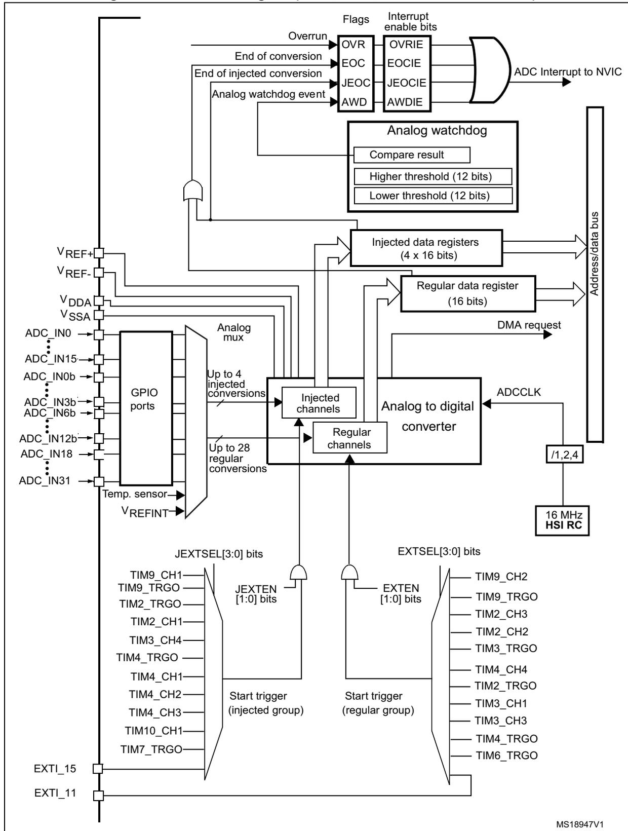
The diagram illustrates the internal architecture of the ADC. On the left, various input pins are shown: VREF+, VREF-, VDDA, VSSA, ADC_IN0 through ADC_IN31, Temp. sensor, and VREFINT. These connect to a central 'Analog mux' block. The 'GPIO ports' block is also connected to this mux. The 'Analog mux' outputs are split into 'Injected channels' (up to 4) and 'Regular channels' (up to 28). Both channel types feed into the 'Analog to digital converter' block. The converter has a 'DMA request' output and receives 'ADCCLK' from a '16 MHz HSI RC' oscillator via a divider (1,2,4). Below the converter, 'JEXTSEL[3:0] bits' and 'JEXTEN [1:0] bits' select the 'Start trigger (injected group)' from sources like TIM9_CH1, TIM9_TRGO, TIM2_TRGO, TIM2_CH1, TIM3_CH4, TIM4_TRGO, TIM4_CH1, TIM4_CH2, TIM4_CH3, TIM10_CH1, TIM7_TRGO, EXTI_15, and EXTI_11. Similarly, 'EXTSEL[3:0] bits' and 'EXTEN [1:0] bits' select the 'Start trigger (regular group)' from sources like TIM9_CH2, TIM9_TRGO, TIM2_CH3, TIM2_CH2, TIM3_TRGO, TIM4_CH4, TIM2_TRGO, TIM3_CH1, TIM3_CH3, TIM4_TRGO, and TIM6_TRGO. The converter outputs data to 'Injected data registers (4 x 16 bits)' and a 'Regular data register (16 bits)', which are connected to an 'Address/data bus'. Above the converter, a 'Flags' block contains OVR, EOC, JEOC, and AWD. Corresponding 'Interrupt enable bits' (OVRIE, EOCIE, JEOCIE, AWDIE) are also present. These flags and enable bits are ANDed to generate an 'ADC Interrupt to NVIC'. An 'Analog watchdog' block contains 'Compare result', 'Higher threshold (12 bits)', and 'Lower threshold (12 bits)', which is connected to the 'ADCCLK' and the 'Address/data bus'.
MS18947V1
12.3.1 ADC power on-off control
The ADC is powered on by setting the ADON bit in the ADC_CR2 register. When the ADON bit is set for the first time, it wakes up the ADC from the Power-down mode.
Conversion starts when either the SWSTART or the JSWSTART bit is set, or in response to an external trigger. These software or hardware triggers must be enabled only when the ADC is ready to convert (ADONS=1).
Resetting the ADON bit stops the conversions and put the ADC in power down mode. In this mode the ADC consumes almost no power. ADONS is cleared after ADON has been synchronized to the ADCCLK clock domain.
Note: Due to the latency introduced by the synchronization between the two clock domains, ADON must be set only when ADONS=0 and it must be cleared only when the ADC is ready to convert (ADONS=1).
Power down configurations (PDI and PDD)
In order to reduce the consumption when the ADC is ready to convert (ADONS=1), the ADC can be automatically powered off when it is not converting, until the next conversion starts depending on the PDI and PDD bits in the ADC_CR1 register. Refer to Section 12.10: Power saving on page 282 for more details.
Using the PDI bit, the user can determine whether the ADC is powered up or down when it is not converting (waiting for a hardware or software trigger event).
Using the PDD bit, the user can determine whether the ADC is powered up or down between 2 conversions (or sequences of conversions) when a delay is inserted (DELS bits).
When PDI=1, ADONS is the image of ADON (same value) as viewed from the ADCCLK clock.
Conversion starts after the ADC power-up time ( \( t_{STAB} \) ) when either the SWSTART or the JSWSTART bit is set, or in response to an external trigger. These software or hardware triggers must be enabled only when the ADC is ready to convert (ADONS=1).
Resetting the ADON bit stops the conversions and places the ADC in a mode where it is no longer supplied.
Note: Due to the latency introduced by the synchronization between the two clock domains, ADON must be set only when ADONS=0 and it must be cleared only when ADONS=1.
12.3.2 ADC clock
To avoid unnecessary consumption while not converting, the ADC digital interface has been designed to operate in a completely independent manner, at its maximum speed using an internal 16 MHz clock source (HSI), whatever the CPU operating frequency (which can range from a few sub-kHz up to 32 MHz).
Note: When entering Stop mode, the ADC analog and digital interfaces remain inactive as the HSI and PCLK2 are disabled. Since the HSI is still deactivated after resuming from Stop mode, the user must enable the HSI as the ADC analog interface clock source and continue using ADC conversions.
The ADCCLK clock is provided by the clock controller. It is generated from the HSI oscillator after a clock divider:
- • by 1 for full speed ( \( f_{ADCCLK} = 16 \) MHz)
- • by 2 for medium speed and by 4 for low speed ( \( f_{ADCCLK} = 4 \) MHz)
Depending on the APB clock (PCLK) frequency, the ADCCLK clock frequency can be higher or lower than PCLK. In particular, when the APB becomes too low, it can become difficult to get the results of conversions at full speed without losing any data (because the data flow is higher than what the CPU or the DMA can handle). This problem can be solved by inserting a delay between 2 conversions or between 2 sequences of conversions in order to give the system enough time to read and save the converted data before the next data arrive. Refer to Section 12.9: Hardware freeze and delay insertion modes for slow conversions on page 279 for more details.
12.3.3 Channel selection
In Cat.1 and Cat.2 devices, there are up to 26 multiplexed channels ADC_IN0..25.
In Cat.3, Cat.4, Cat.5 and Cat.6 devices there are up to 42 multiplexed channels organized in 2 banks. Channels ADC_IN0 to ADC_IN31 are available in Bank A and channels ADC_IN0b to ADC_IN31b are available in Bank B. The bank selection is configured by the ADC_CFG bit in the ADC_CR2 register. Temperature sensor input, internal voltage reference input and selected external analog inputs i.e. ADC_IN4 / ADC_IN4b () are available in both banks. For details see Table 41: I/O groups and selection .
It is possible to organize the conversions in two groups: regular and injected. A group consists of a sequence of conversions that can be done in any order and on any available input channels from the selected bank. For instance, it is possible to implement the conversion sequence in the following order: ADC_IN3, ADC_IN8, ADC_IN2, ADC_IN2, ADC_IN0, ADC_IN2.
- • A regular group is composed of up to 28 conversions. The regular channels and their order in the conversion sequence must be selected in the ADC_SQRx registers. The total number of conversions, which can be up to 28 in the regular group must be written in the L[4:0] bits in the ADC_SQR1 register.
- • An injected group is composed of up to 4 conversions. The injected channels and their order in the conversion sequence must be selected in the ADC_JSQR register. The total number of conversions, which can be up to 4 in the injected group must be written in the L[1:0] bits in the ADC_JSQR register.
Note: If the ADC_SQRx register is modified during a regular conversion or the ADC_JSQR register is modified during an injected conversion, the current conversion is reset and the ADC waits for a new start pulse. If the conversion that is reset is an injected conversion that had interrupted a regular conversion, then the regular conversion is resumed.
Up to 6 direct channels are connected to the input switch matrix of ADC allowing to sample at the full speed of 1 MSamples/s. The rest of the input channels are multiplexed through routing interface reducing speed to 800 kSamples/s. For more information see Section 8.2: RI main features .
Temperature sensor, V REFINT internal channels
The temperature sensor is connected to channel ADC_IN16 and the internal reference voltage V REFINT is connected to ADC_IN17. These two internal channels can be selected and converted as injected or regular channels.
12.3.4 Single conversion mode
In Single conversion mode the ADC does one conversion. This mode is started with the CONT bit in the ADC_CR2 at 0 by either:
- • setting the SWSTART bit in the ADC_CR2 register (for a regular channel only)
- • setting the JSWSTART bit (for an injected channel)
- • external trigger (for a regular or injected channel)
Once the conversion of the selected channel is complete:
- • If a regular channel was converted (converted channel is selected by the SQ1[4:0] bits in the SQR5 register):
- – The converted data are stored into the 16-bit ADC_DR register
- – The EOC (end of conversion) flag is set
- – An interrupt is generated if the EOCIE bit is set
- • If an injected channel was converted (converted channel is selected by the JSQ1[4:0] bits in the JSQR register):
- – The converted data are stored into the 16-bit ADC_JDR1 register
- – The JEOC (end of conversion injected) flag is set
- – An interrupt is generated if the JEOCIE bit is set
Then the ADC stops.
12.3.5 Continuous conversion mode
In continuous conversion mode, the ADC starts a new conversion as soon as it finishes one. This mode is started with the CONT bit at 1 either by external trigger or by setting the SWSTART bit in the ADC_CR2 register (for regular channels only).
After each conversion:
- • If a regular channel was converted (converted channel is selected by the SQ1[4:0] bits in the SQR5 register):
- – The last converted data are stored into the 16-bit ADC_DR register
- – The EOC (end of conversion) flag is set
- – An interrupt is generated if the EOCIE bit is set
Note: Injected channels cannot be converted continuously. The only exception is when an injected channel is configured to be converted automatically after regular channels in continuous mode (using JAUTO bit), refer to Auto-injected conversion section ).
12.3.6 Timing diagram
As shown in Figure 41 , the ADC needs a stabilization time ( \( t_{STAB} \) ) before it can actually convert. The ADONS bit is set when a conversion can be triggered. A conversion is launched when the SWSTART bit is set (or when an external trigger is detected). After the conversion time (programmable sampling time + 12 ADCCLK clock cycles for 12-bit data), the EOC flag is set and the ADC data register contains the result of the conversion. Note that some delays are needed to resynchronize the different signals from one clock domain to the other.
Figure 41. Timing diagram (normal mode, PDI=0)
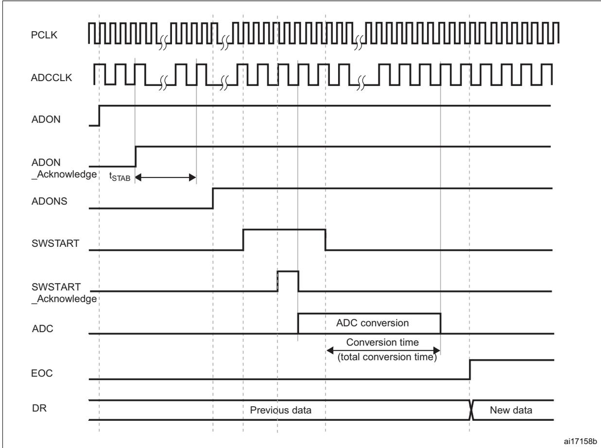
The timing diagram shows the following signals and their relationships:
- PCLK : System clock, shown as a continuous high-frequency square wave.
- ADCCLK : ADC clock, derived from PCLK, shown as a lower-frequency square wave.
- ADON : ADC On/Off bit. A rising edge turns the ADC on.
- ADON_Acknowledge : Signal indicating the ADC is on. A time interval \( t_{STAB} \) is shown between the ADON rising edge and the signal becoming stable.
- ADONS : ADC Software Start bit. A rising edge initiates a conversion sequence.
- SWSTART : Software Start bit.
- SWSTART_Acknowledge : Signal indicating the start of the conversion sequence.
- ADC : Analog-to-digital conversion signal. A rising edge starts the conversion, and a falling edge ends it. The duration is labeled "ADC conversion" and "Conversion time (total conversion time)".
- EOC : End of Conversion signal. It goes high when the conversion is complete.
- DR : Data Register. It contains "Previous data" until the conversion is complete, at which point it is updated with "New data".
ai17158b
12.3.7 Analog watchdog
The AWD analog watchdog status bit is set if the analog voltage converted by the ADC is below a lower threshold or above a higher threshold. These thresholds are programmed in the 12 least significant bits of the ADC_HTR and ADC_LTR 16-bit registers. An interrupt can be enabled by using the AWDIE bit in the ADC_CR1 register.
The threshold value is independent of the alignment selected by the ALIGN bit in the ADC_CR2 register. The analog voltage is compared to the lower and higher thresholds before alignment.
Table 59 shows how the ADC_CR1 register should be configured to enable the analog watchdog on one or more channels.
Figure 42. Analog watchdog's guarded area
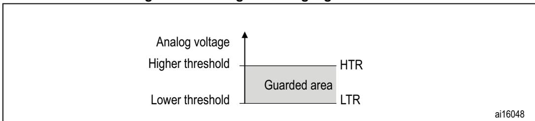
The graph shows the "Analog voltage" on the vertical axis. Two horizontal lines represent the thresholds: "Higher threshold" (HTR) and "Lower threshold" (LTR). The region between these two thresholds is shaded and labeled "Guarded area".
ai16048
Table 59. Analog watchdog channel selection
| Channels guarded by the analog watchdog | ADC_CR1 register control bits (x = don't care) | ||
|---|---|---|---|
| AWDSGL bit | AWDEN bit | JAWDEN bit | |
| None | x | 0 | 0 |
| All injected channels | 0 | 0 | 1 |
| All regular channels | 0 | 1 | 0 |
| All regular and injected channels | 0 | 1 | 1 |
| Single (1) injected channel | 1 | 0 | 1 |
| Single (1) regular channel | 1 | 1 | 0 |
| Single (1) regular or injected channel | 1 | 1 | 1 |
1. Selected by the AWDCH[4:0] bits
12.3.8 Scan mode
This mode is used to scan a group of analog channels.
The Scan mode is selected by setting the SCAN bit in the ADC_CR1 register. Once this bit has been set, the ADC scans all the channels selected in the ADC_SQRx registers (for regular channels) or in the ADC_JSQR register (for injected channels). All the channels to be converted must be located in the same bank as the ADC_CFG bit is stable during the scan. A single conversion is performed for each channel of the group. After each end of conversion, the next channel in the group is converted automatically. If the CONT bit in the ADC_CR2 register is set, regular channel conversion does not stop at the last selected channel in the group but continues again from the first selected channel.
If the DMA bit is set, the direct memory access (DMA) controller is used to transfer the data converted from the regular group of channels (stored in the ADC_DR register) to memory after each regular channel conversion.
The EOC bit is set in the ADC_SR register if:
- • At the end of each regular group sequence the EOCS bit is cleared to 0
- • At the end of each regular channel conversion the EOCS bit is set to 1
The data converted from an injected channel is always stored into the ADC_JDRx registers.
12.3.9 Injected channel management
Triggered injected conversion
To use triggered injection, the JAUTO bit must be cleared in the ADC_CR1 register.
- 1. Start the conversion of a group of injected channels either by external trigger or by setting the JSWSTART bit in the ADC_CR2 register.
- 2. If an external injected trigger occurs or if the JSWSTART bit is set during the conversion of a regular group of channels, the current conversion is reset and the injected channel sequence switches to Scan-once mode.
- 3. Then, the regular conversion of the regular group of channels is resumed from the last interrupted regular conversion.
If a regular event occurs during an injected conversion, the injected conversion is not
interrupted but the regular sequence is executed at the end of the injected sequence. Figure 43 shows the corresponding timing diagram.
Note: When using triggered injection, one must ensure that the interval between trigger events is longer than the injection sequence. For instance, if the sequence length is 30 ADC clock cycles (that is two conversions with a sampling time of 3 clock periods), the minimum interval between triggers must be 31 ADC clock cycles.
Figure 43. Injected conversion latency
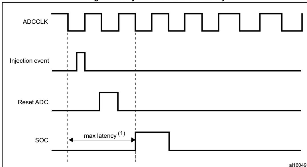
1. The maximum latency value can be found in the electrical characteristics of the STM32L1xxxx datasheet.
Auto-injected conversion
If the JAUTO bit is set, then the channels in the injected group are automatically converted after the regular group of channels. This can be used to convert a sequence of up to 31 conversions programmed in the ADC_SQRx and ADC_JSQR registers.
In this mode, external trigger on injected channels must be disabled.
If the CONT bit is also set in addition to the JAUTO bit, regular channels followed by injected channels are continuously converted.
Note: It is not possible to use both the auto-injected and discontinuous modes simultaneously.
12.3.10 Discontinuous mode
Regular group
This mode is enabled by setting the DISCEN bit in the ADC_CR1 register. It can be used to convert a short sequence of n conversions ( \( n \leq 8 \) ) that is part of the sequence of conversions selected in the ADC_SQRx registers. The value of n is specified by writing to the DISCNUM[2:0] bits in the ADC_CR1 register.
When an external trigger occurs, it starts the next n conversions selected in the ADC_SQRx registers until all the conversions in the sequence are done. The total sequence length is defined by the L[4:0] bits in the ADC_SQR1 register.
Example:
n = 3, regular channels to be converted = 0, 1, 2, 3, 6, 7, 9, 10
1st trigger: sequence converted 0, 1, 2
2nd trigger: sequence converted 3, 6, 7
3rd trigger: sequence converted 9, 10 and an EOC event generated
4th trigger: sequence converted 0, 1, 2
Note: When a regular group is converted in discontinuous mode, no rollover occurs.
When all subgroups are converted, the next trigger starts the conversion of the first subgroup. In the example above, the 4th trigger reconverts the channels 0, 1 and 2 in the 1st subgroup.
Injected group
This mode is enabled by setting the JDISCEN bit in the ADC_CR1 register. It can be used to convert a short sequence of n conversions ( \( n \leq 3 \) ) part of the sequence of conversions selected in the ADC_JSQR registers. The value of n is specified by writing to the DISCNUM[2:0] bits in the ADC_CR1 register.
When an external trigger occurs, it starts the next channel conversions selected in the ADC_JSQR registers until all the conversions in the sequence are done. The total sequence length is defined by the JL[1:0] bits in the ADC_JSQR register.
Example:
n = 1, injected channels to be converted = 1, 2, 3
1st trigger: channel 1 converted
2nd trigger: channel 2 converted
3rd trigger: channel 3 converted and EOC and JEOC events generated
4th trigger: channel 1
Note: When all injected channels are converted, the next trigger starts the conversion of the first injected channel. In the example above, the 4th trigger reconverts the 1st injected channel 1.
It is not possible to use both the auto-injected and discontinuous modes simultaneously.
Discontinuous mode must not be set for regular and injected groups at the same time.
12.4 Data alignment
The ALIGN bit in the ADC_CR2 register selects the alignment of the data stored after conversion. Data can be right- or left-aligned as shown in Figure 44 and Figure 45 .
The converted data value from the injected group of channels is decreased by the user-defined offset written in the ADC_JOFRx registers so the result can be a negative value. The SEXT bit represents the extended sign value.
For channels in a regular group, no offset is subtracted so only twelve bits are significant.
Figure 44. Right alignment of 12-bit data
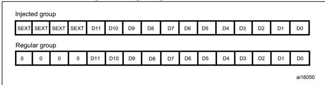
| Injected group | |||||||||||||||
| SEXT | SEXT | SEXT | SEXT | D11 | D10 | D9 | D8 | D7 | D6 | D5 | D4 | D3 | D2 | D1 | D0 |
| Regular group | |||||||||||||||
| 0 | 0 | 0 | 0 | D11 | D10 | D9 | D8 | D7 | D6 | D5 | D4 | D3 | D2 | D1 | D0 |
ai16050
Figure 45. Left alignment of 12-bit data
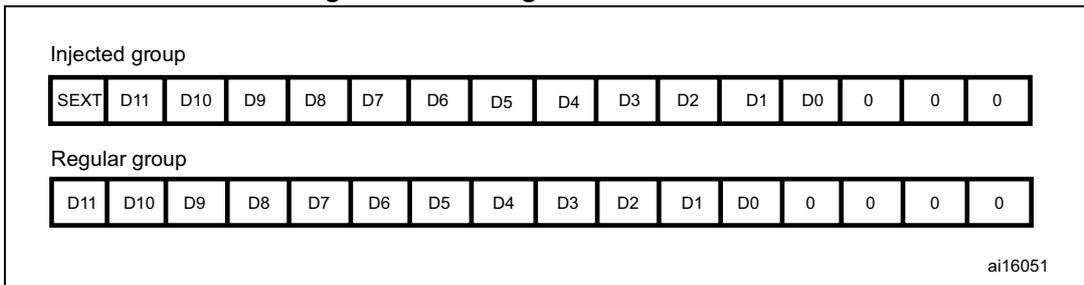
| Injected group | |||||||||||||||
| SEXT | D11 | D10 | D9 | D8 | D7 | D6 | D5 | D4 | D3 | D2 | D1 | D0 | 0 | 0 | 0 |
| Regular group | |||||||||||||||
| D11 | D10 | D9 | D8 | D7 | D6 | D5 | D4 | D3 | D2 | D1 | D0 | 0 | 0 | 0 | 0 |
ai16051
Special case: when left-aligned, the data are aligned on a half-word basis except when the resolution is set to 6-bit. In that case, the data are aligned on a byte basis as shown in Figure 46.
Figure 46. Left alignment of 6-bit data
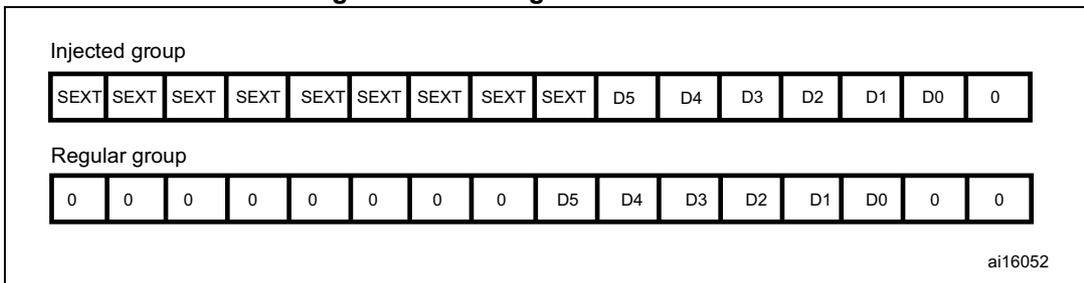
| Injected group | |||||||||||||||
| SEXT | SEXT | SEXT | SEXT | SEXT | SEXT | SEXT | SEXT | SEXT | D5 | D4 | D3 | D2 | D1 | D0 | 0 |
| Regular group | |||||||||||||||
| 0 | 0 | 0 | 0 | 0 | 0 | 0 | 0 | D5 | D4 | D3 | D2 | D1 | D0 | 0 | 0 |
ai16052
12.5 Channel-wise programmable sampling time
The ADC samples the input voltage for a number of ADCCLK cycles that can be modified using the SMP[2:0] bits in the ADC_SMPRx registers (x = 1 to 3). Each channel of a given bank can be sampled with a different sampling time. Nevertheless, the sampling time selection is shared between the 2 banks.
The total conversion time is calculated as follows:
Example:
With ADCCLK = 16 MHz and sampling time = 4 cycles:
12.6 Conversion on external trigger
Conversion can be triggered by an external event (e.g. timer capture, EXTI line). If the EXTEN[1:0] control bits (for a regular conversion) or JEXTEN[1:0] bits (for an injected conversion) are different from “0b00”, then external events are able to trigger a conversion with the selected edge. Table 60 provides the correspondence between the EXTEN[1:0] and JEXTEN[1:0] values and the trigger edge.
Table 60. Configuring the trigger edge detection
| Source | EXTEN[1:0] / JEXTEN[1:0] |
|---|---|
| Trigger detection disabled | 00 |
| Detection on the rising edge | 01 |
| Detection on the falling edge | 10 |
| Detection on both the rising and falling edges | 11 |
Note: The edge detection of the external trigger can be changed on the fly.
The EXTSEL[3:0] and JEXTSEL[3:0] control bits are used to select which out of 16 possible events can trigger conversion for the regular and injected groups.
Table 61 gives the possible external trigger for regular conversion.
Table 61. External trigger for regular channels
| Source | Type | EXTSEL[3:0] |
|---|---|---|
| TIM9_CC2 event | Internal signal from on-chip timers | 0000 |
| TIM9_TRGO event | 0001 | |
| TIM2_CC3 event | 0010 | |
| TIM2_CC2 event | 0011 | |
| TIM3_TRGO event | 0100 | |
| TIM4_CC4 event | 0101 | |
| TIM2_TRGO event | 0110 | |
| TIM3_CC1 event | 0111 | |
| TIM3_CC3 event | 1000 | |
| TIM4_TRGO event | 1001 | |
| TIM6_TRGO event | NA | 1010 |
| Reserved | 1011 | |
| Reserved | 1100 | |
| Reserved | 1101 | |
| Reserved | 1110 | |
| EXTI line11 | External pin | 1111 |
Table 62 gives the possible external trigger for injected conversion.
Table 62. External trigger for injected channels
| Source | Type | EXTSEL[3:0] |
|---|---|---|
| TIM9_CC1 event | Internal signal from on-chip timers | 0000 |
| TIM9_TRGO event | 0001 | |
| TIM2_TRGO event | 0010 | |
| TIM2_CC1 event | 0011 | |
| TIM3_CC4 event | 0100 | |
| TIM4_TRGO event | 0101 | |
| TIM4_CC1 event | 0110 | |
| TIM4_CC2 event | 0111 | |
| TIM4_CC3 event | 1000 | |
| TIM10_CC1 event | 1001 | |
| TIM7_TRGO event | 1010 | |
| Reserved | NA | 1011 |
| Reserved | 1100 | |
| Reserved | 1101 | |
| Reserved | 1110 | |
| EXTI line15 | External pin | 1111 |
A regular group conversion can be interrupted by an injected trigger.
Note: The trigger selection can be changed on the fly. When this is done, however, trigger detection is disabled for a period of 2 PCLK cycles. This is to avoid spurious detections during the transition.
The interval between trigger events must be longer than:
- • the sequence for regular conversions
- • the sequence + 1 ADCCLK cycle for injected conversions
For instance, if the sequence length is 32 ADC clock cycles (that is two conversions with a 4 clock-period sampling time), the minimum interval between regular triggers must be greater than 32 ADC clock cycles and the interval between injected triggers must be greater than 33 ADC clock cycles.
12.7 Aborting a conversion
12.7.1 Injected channels
An injected conversion or a sequence of conversions can be stopped by writing to the JSQR register (the JL[1:0] bitfield has to be written with its current value). Then any ongoing injected conversion aborts and any pending trigger is reset. A new injected conversion can start when a new hardware or software trigger occurs.
After aborting an injected conversion, the system requires a few clock cycles before a new injected conversion can start (3 to 5 ADC clock cycles + 2 to 5 APB clock cycles). To meet this requirement, JSWSTART should not be set before JCNR=0.
12.7.2 Regular channels
A regular conversion or a sequence of conversions can be stopped by writing to any of the SQR1 to SQR5 registers (if SQR1 is written, the L[4:0] bitfield has to be written with its current value). The ADC then behaves in the same way as in the case of injected conversions (see Section 12.7.2: Regular channels ).
If several of the SQRi registers have to be written in order to configure a new sequence, no conversion should be launched between the different write accesses. In this case, the following sequence must be applied:
- 1. Disable the external triggers by writing the EXTEN bits to 00 (when external triggers are used)
- 2. Change the sequence configuration (by writing to the SQRi registers)
- 3. Wait for RCNR=0 in the ADC_SR register
- 4. Enable the external trigger or set the SWSTART bit
12.8 Conversion resolution
It is possible to perform faster conversion by reducing the ADC resolution. The RES[1:0] bits are used to select the number of bits available in the data register. The minimal conversion time for each resolution, when the sampling time is 4 cycles, is then as follows:
- • for 12-bit resolution : \( 12 + 4 = 16 \) cycles
- • for 10-bit resolution : \( 11 + 4 = 15 \) cycles
- • for 8-bit resolution : \( 9 + 4 = 13 \) cycles
- • for 6-bit resolution : \( 7 + 4 = 11 \) cycles
12.9 Hardware freeze and delay insertion modes for slow conversions
When the APB clock is not fast enough to manage the data rate, a delay can be introduced between conversions to reduce this data rate. The delay is inserted after each regular conversion and after each sequence of injected conversions as, during conversion, a trigger event (for the same group of conversions) occurring during this delay is ignored.
No delay is inserted between conversions of different groups (a regular conversion followed by an injected conversion or conversely):
- • If an injected trigger occurs during the delay of a regular conversion, the injected conversion starts immediately.
- • If a regular conversion is to be resumed after being interrupted by an injected sequence, it starts as soon as the delay of the previous regular conversion is finished.
The behavior is slightly different in auto-injected mode where a new regular conversion can start only when the delay of the previous injected conversion has ended. This is to ensure that the software can read all the data of a given sequence before starting a new sequence. In this mode, a regular trigger is ignored if it occurs during the delay that follows a regular
conversion. It is however considered pending if it occurs after this delay, even if it occurs during an injected sequence or the delay that follows it. The conversion then starts at the end of the delay of the injected sequence.
The length of the delay is configured using the DELS[2:0] bits in the ADC_CR2 register. Two cases should be considered:
- • ADC freeze mode:
When DELS[2:0]=001, a new conversion can start only if all the previous data of the same group have been treated:- – for a regular conversion: once the ADC_DR register has been read or if the EOC bit has been cleared
- – for an injected conversion: when the JEOC bit has been cleared
- • ADC delay insertion mode:
When DELS[2:0]>001, a new conversion can start only after a given number of APB clock cycles after the end of the previous conversion in the same group.
Figure 47. ADC freeze mode
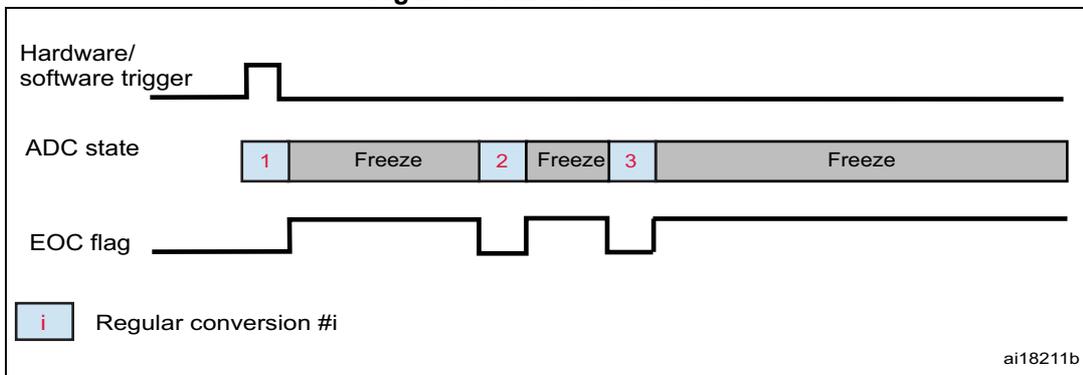
The diagram illustrates the timing for ADC freeze mode. It consists of three horizontal timelines:
- Hardware/software trigger: A signal that goes high to start a conversion and returns low.
- ADC state: Shows a sequence of regular conversions (labeled 1, 2, 3) and 'Freeze' periods. Conversion 1 starts when the trigger is high. After conversion 1, the state becomes 'Freeze'. Conversion 2 starts only after the EOC flag for conversion 1 is cleared. After conversion 2, it becomes 'Freeze' again. Conversion 3 starts only after the EOC flag for conversion 2 is cleared. After conversion 3, it becomes 'Freeze' again. The 'Freeze' periods continue until a new conversion is started by the trigger.
- EOC flag: A flag that goes high when a conversion is complete and returns low when the data is read from the ADC_DR register. It is shown going high at the end of each conversion (1, 2, 3) and returning low when the data is read.
Legend: A blue box with the letter 'i' represents 'Regular conversion #i'.
ai18211b
12.9.1 Inserting a delay after each regular conversion
When enabled, a delay is inserted at the end of each regular conversion before a new regular conversion can start. It gives time to read the converted data in the ADC_DR register before a new regular conversion is completed. The length of the delay is configured by the DELS[2:0] bits. Figure 48 shows an example of continuous regular conversions where a 10 PCLK cycle delay is inserted after each conversion.
Note: When ADC_CR2_EOCS = 1, the delay is inserted after each sequence of regular group conversions.
Figure 48. Continuous regular conversions with a delay
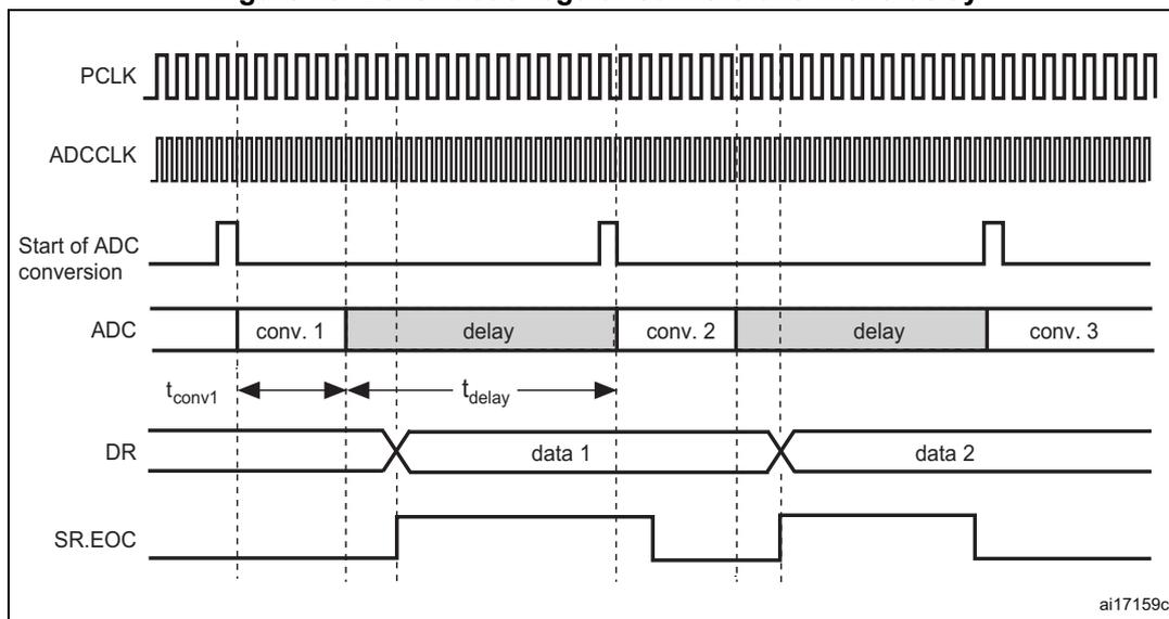
- 1. \( t_{conv1} \) : including sampling and conversion times (for instance 16 ADC clock cycles with the minimum sampling time)
- 2. \( t_{delay} \) : delay from the end of a conversion to the start of the next conversion (number of PCLK periods configured with the DELS[2:0] bits) + delay to synchronize the end of conversion (0 to 1 PCLK clock cycles) + delay to synchronize the end of delay (2 or 3 ADC clock cycles).
12.9.2 Inserting a delay after each sequence of auto-injected conversions
When enabled, a delay is inserted at the end of each sequence of injected conversions. Up to 5 conversion results can be stored into the ADC_DR and the ADC_JDRx registers. The length of the delay is configured by the DELS[2:0] bits. Figure 49 shows an example of continuous conversions (the CONT bit is set) where a delay is inserted after each sequence of injected conversions. Here the JAUTO bit is set and the sequence ends after the last injected conversion (the sequence is made of 1 regular conversion + 2 injected conversions).
Figure 49. Continuous conversions with a delay between each conversion
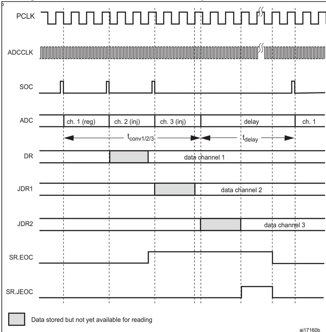
The timing diagram shows the following signals and timing parameters:
- PCLK: System clock signal.
- ADCCLK: ADC clock signal, shown as a high-frequency signal.
- SOC: Start of Conversion signal, triggered by a rising edge.
- ADC: Sequence of conversions: ch. 1 (reg), ch. 2 (inj), ch. 3 (inj), delay, ch. 1.
- DR: Data Register for channel 1. A shaded area indicates data is stored but not yet available.
- JDR1: Injected Data Register 1 for channel 2. A shaded area indicates data is stored but not yet available.
- JDR2: Injected Data Register 2 for channel 3. A shaded area indicates data is stored but not yet available.
- SR.EOC: End of Conversion flag for the regular sequence.
- SR.JEOC: End of Conversion flag for the injected sequence.
- \( t_{conv1/2/3} \) : Time for one conversion (sampling + conversion) for channels 1, 2, and 3.
- \( t_{delay} \) : Delay time between the end of one sequence and the start of the next.
Data stored but not yet available for reading
ai17160b
- 1. \( t_{conv1/2/3} \) : including sampling and conversion times for channels 1, 2 and 3.
- 2. \( t_{delay} \) : delay from the end of the previous sequence to the start of the new sequence (number of PCLK periods configured with the DELS bits) + delay to synchronize the end of conversion (0 to 1 PCLK clock cycles) + delay to synchronize the end of delay (2 or 3 ADC clock cycles).
12.10 Power saving
ADC power-on and power-off can be managed by hardware to cut the consumption when the ADC is not converting. The ADC can be powered down:
- • during the delay described above (when the PDD bit is set). Then the ADC is powered up again at the end of the delay and/or
- • when the ADC is waiting for a trigger event (when the PDI bit is set). In this case the ADC is powered up at the next trigger event.
The ADC needs a certain time to start up before a conversion can actually be launched. This startup time must be taken into account before selecting the automatic power control modes or when configuring the delay. For this reason, it is also more efficient (from the power point of view and when possible) when scanning several channels to launch a sequence of several conversions and stop the consumption after the sequence, than when launching each conversion one by one with a delay after each conversion.
For a given sequence of conversions, the ADCCLK clock must be enabled before launching the first conversion, and be present until the EOC bit (or the JEOC bit in case of injected channels) is set.
Figure 50, Figure 51 and Figure 52 show examples of power management in different configurations. ADON=1 in all these examples.
Figure 50. Automatic power-down control: example 1
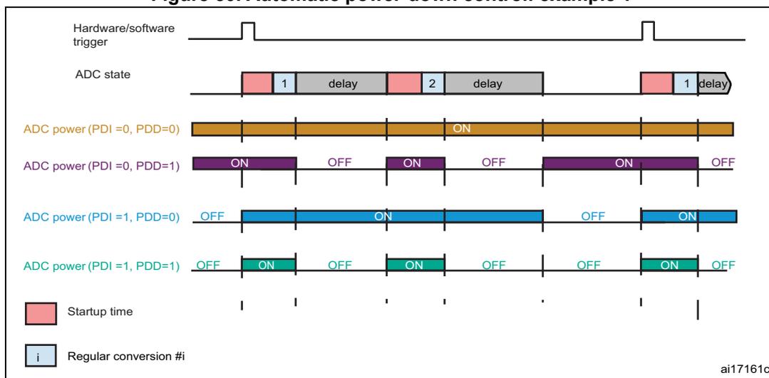
Figure 50 is a timing diagram illustrating automatic power-down control. It shows the relationship between a hardware/software trigger, the ADC state, and the ADC power levels for four different configurations: PDI=0, PDD=0; PDI=0, PDD=1; PDI=1, PDD=0; and PDI=1, PDD=1. The ADC state is shown as a sequence of startup times (red) and regular conversions (blue, labeled 1 and 2) separated by delays (grey). The ADC power levels are shown as horizontal bars indicating ON and OFF states. The legend indicates that red represents startup time and blue represents regular conversion #i.
Figure 51. Automatic power-down control: example 2
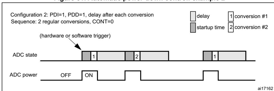
Figure 51 is a timing diagram illustrating automatic power-down control for a specific configuration: PDI=1, PDD=1, with a delay after each conversion. The sequence consists of 2 regular conversions (CONT=0). The diagram shows the ADC state (startup time, conversion #1, delay, conversion #2, delay) and the corresponding ADC power levels (OFF, ON, OFF). The legend indicates that grey represents delay, red represents startup time, and blue represents regular conversion #i.
Figure 52. Automatic power-down control: example 3
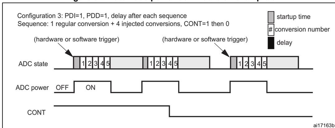
Configuration 3: PDI=1, PDD=1, delay after each sequence
Sequence: 1 regular conversion + 4 injected conversions, CONT=1 then 0
(hardware or software trigger) (hardware or software trigger)
ADC state
ADC power
CONT
startup time
# conversion number
delay
ai17163b
12.11 Data management and overrun detection
12.11.1 Using the DMA
Since converted regular channel values are stored into a unique data register, it is useful to use DMA for conversion of more than one regular channel. This avoids the loss of the data already stored in the ADC_DR register.
When the DMA mode is enabled (DMA bit set to 1 in the ADC_CR2 register), after each conversion of a regular channel, a DMA request is generated. This allows the transfer of the converted data from the ADC_DR register to the destination location selected by the software.
Despite this, if data are lost (overrun), the OVR bit in the ADC_SR register is set and an interrupt is generated (if the OVRIE enable bit is set). DMA transfers are then disabled and DMA requests are no longer accepted. In this case, if a DMA request is made, the regular conversion in progress is aborted and further regular triggers are ignored. It is then necessary to clear the OVR flag and the DMAEN bit in the used DMA stream, and to re-initialize both the DMA and the ADC to have the wanted converted channel data transferred to the right memory location. Only then can the conversion be resumed and the data transfer, enabled again. Injected channel conversions are not impacted by overrun errors.
When OVR = 1 in DMA mode, the DMA requests are blocked after the last valid data have been transferred, which means that all the data transferred to the RAM can be considered as valid.
At the end of the last DMA transfer (number of transfers configured in the DMA controller's DMA_SxRTR register):
- • No new DMA request is issued to the DMA controller if the DDS bit is cleared to 0 in the ADC_CR2 register (this avoids generating an overrun error). However the DMA bit is not cleared by hardware. It must be written to 0, then to 1 to start a new transfer.
- • Requests can continue to be generated if the DDS bit is set to 1. This allows configuring the DMA in double-buffer circular mode.
12.11.2 Managing a sequence of conversions without using the DMA
If the conversions are slow enough, the conversion sequence can be handled by the software. In this case the EOCS bit must be set in the ADC_CR2 register for the EOC status
bit to be set at the end of each conversion, and not only at the end of the sequence. When EOCS = 1, overrun detection is automatically enabled. Thus, each time a conversion is complete, EOC is set and the ADC_DR register can be read. The overrun management is the same as when the DMA is used.
12.11.3 Conversions without reading all the data
It may be useful to let the ADC convert one or more channels without reading the data each time (if there is an analog watchdog for instance). For that, the DMA must be disabled (DMA = 0) and the EOC bit must be set at the end of a sequence only (EOCS = 0). In this configuration no overrun error is reported if a conversion finishes when the result of the previous conversion has not been read.
12.11.4 Overrun detection
Overrun detection is always enabled. It takes place before the data are synchronized to the APB clock.
Note: Only regular channel conversions generate overrun errors.
At the end of a conversion, the result is stored into an intermediate buffer (in the ADC clock domain) until it is transferred to the data register (ADC_DR, in the APB clock domain). If new data arrive before the previous data are transferred, the new data are lost and an overrun error is detected. The OVR bit is set in the ADC_SR register and an interrupt is generated if the OVRIE bit is set.
This may occur in two cases:
- • either the delay is not properly set with respect to the APB clock frequency (the delay is too short to synchronize the data), or
- • the previous data could not be synchronized to the APB clock because the ADC_DR register is not empty (when DMA=1 or EOCS=1). Indeed, in these modes, the contents of the ADC_DR register cannot be overwritten and so the register always contains the last valid data. ADC_DR is emptied by reading it or by clearing the EOC bit in the ADC_SR register.
Note: An overrun may happen to be detected just after clearing the DMA (or EOCS) when the last data transferred by the DMA are read very late, which causes the next data to be lost. After clearing the OVR bit, the software should not launch a new regular conversion until RCNR=0 in the ADC_SR register.
12.12 Temperature sensor and internal reference voltage
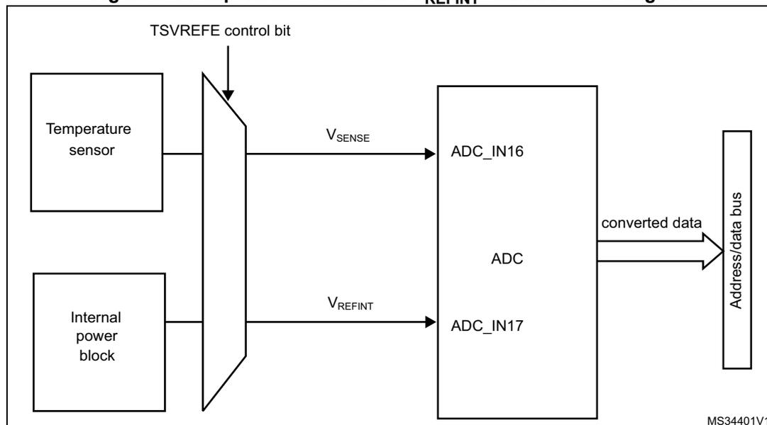
The temperature sensor can be used to measure the junction temperature ( \( T_j \) ) of the device. The temperature sensor is internally connected to the ADC_IN16 input channel which is used to convert the sensor's output voltage to a digital value. When not in use, the sensor can be put in power down mode.
The temperature sensor output voltage changes linearly with temperature, however its characteristics may vary significantly from chip to chip due to the process variations. To improve the accuracy of the temperature sensor (especially for absolute temperature measurement), calibration values are individually measured for each part by ST during production test and stored in the system memory area. Refer to the specific device datasheet for additional information.
The internal voltage reference ( \( V_{REFINT} \) ) provides a stable (bandgap) voltage output for the ADC and Comparators. \( V_{REFINT} \) is internally connected to the ADC_IN17 input channel. The precise voltage of \( V_{REFINT} \) is individually measured for each part by ST during production test and stored in the system memory area.
Figure 53 shows the block diagram of connections between the temperature sensor, the internal voltage reference and the ADC.
The TSVREFE bit must be set to enable the conversion of ADC_IN16 (temperature sensor) and the conversion of ADC_IN17 ( \( V_{REFINT} \) ).
Figure 53. Temperature sensor and \( V_{REFINT} \) channel block diagram
Reading the temperature
- 1. Select the ADC_IN16 input channel.
- 2. Select appropriate sampling time specified in device datasheet ( \( T_{S\_temp} \) )
- 3. Set the TSVREFE bit in the ADC_CCR register to wake up the temperature sensor from power-down mode and wait for its stabilization time ( \( t_{START} \) ).
- 4. Start the ADC conversion.
- 5. Read the resulting data in the ADC_DR register.
- 6. Calculate the temperature using the following formulae:
Where:
- • \( \text{TS\_CAL2} \) is the temperature sensor calibration value acquired at \( 110^\circ\text{C} \)
- • \( \text{TS\_CAL1} \) is the temperature sensor calibration value acquired at \( 30^\circ\text{C} \)
- • \( \text{TS\_DATA} \) is the actual temperature sensor output value converted by ADC
Refer to the specific device datasheet for more information about \( \text{TS\_CAL1} \) and \( \text{TS\_CAL2} \) calibration points.
Note: The sensor has a startup time after waking from power down mode before it can output \( V_{SENSE} \) at the correct level. The ADC also has a startup time after power-on, so to minimize the delay, the ADON and TSVREFE bits should be set at the same time.
Calculating the actual \( V_{DDA} \) voltage using the internal reference voltage
The \( V_{DDA} \) power supply voltage applied to the microcontroller may be subject to variation or not precisely known. The embedded internal voltage reference ( \( V_{REFINT} \) ) and its calibration data acquired by the ADC during the manufacturing process at \( V_{DDA} = 3\text{ V} \) can be used to evaluate the actual \( V_{DDA} \) voltage level.
The following formula gives the actual \( V_{DDA} \) voltage supplying the device:
Where:
- • \( VREFINT\_CAL \) is the \( V_{REFINT} \) calibration value
- • \( VREFINT\_DATA \) is the actual \( V_{REFINT} \) output value converted by ADC
Converting a supply-relative ADC measurement to an absolute voltage value
The ADC is designed to deliver a digital value corresponding to the ratio between the analog power supply and the voltage applied on the converted channel. For most application use cases, it is necessary to convert this ratio into a voltage independent of \( V_{DDA} \) . For applications where \( V_{DDA} \) is known and ADC converted values are right-aligned you can use the following formula to get this absolute value:
For applications where \( V_{DDA} \) value is not known, you must use the internal voltage reference and \( V_{DDA} \) can be replaced by the expression provided in Section : Calculating the actual \( V_{DDA} \) voltage using the internal reference voltage , resulting in the following formula:
Where:
- • \( VREFINT\_CAL \) is the \( V_{REFINT} \) calibration value
- • \( ADC\_DATA_x \) is the value measured by the ADC on channel x (right-aligned)
- • \( VREFINT\_DATA \) is the actual \( V_{REFINT} \) output value converted by the ADC
- • \( FULL\_SCALE \) is the maximum digital value of the ADC output. For example with 12-bit resolution, it is \( 2^{12} - 1 = 4095 \) or with 8-bit resolution, \( 2^8 - 1 = 255 \) .
Note: If ADC measurements are done using an output format other than 12-bit right-aligned, all the parameters must first be converted to a compatible format before the calculation is done.
12.13 Internal reference voltage ( \( V_{REFINT} \) ) conversion
The internal reference voltage is internally connected to the V REFINT channel. This analog input channel is used to convert the internal reference voltage into a digital value.
The TSVREFE bit in the ADC_CCR register must be set to enable the internal reference voltage (and also the Temperature sensor). This reference voltage must be enabled only if its conversion is required.
The internal reference voltage is factory measured and the result of the ADC conversion is stored in a specific data address : the VREFINT_Factory_CONV byte.
12.14 ADC interrupts
An interrupt can be produced on the end of conversion for regular and injected groups, when the analog watchdog status bit is set and when the overrun status bit is set. Separate interrupt enable bits are available for flexibility.
Five other flags are present in the ADC_SR register, but there is no interrupt associated with them:
- • JCNR (injected channel not ready)
- • RCNR (regular channel not ready)
- • ADONS (ADON status)
- • JSTRT (Start of conversion for channels of an injected group)
- • STRT (Start of conversion for channels of a regular group)
Figure 54. ADC flags and interrupts
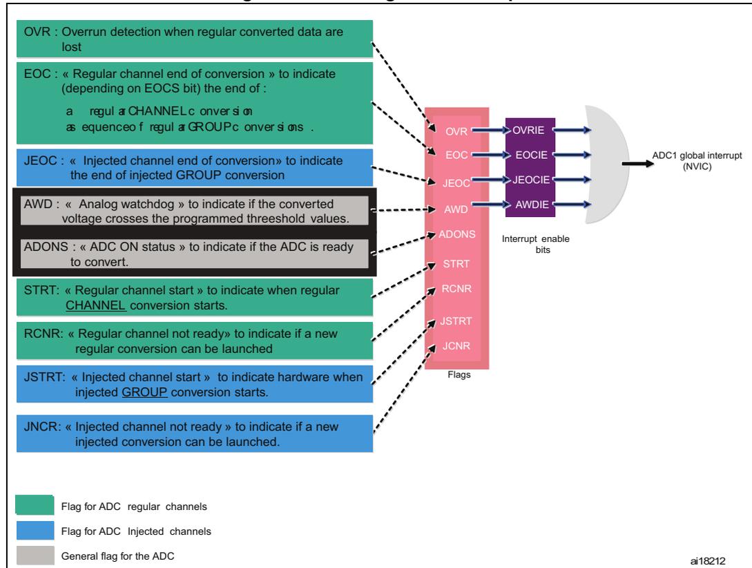
The diagram illustrates the relationship between ADC flags and interrupt enable bits. On the left, a list of flags is provided with their descriptions and color-coded categories:
- OVR : Overrun detection when regular converted data are lost
- EOC
: « Regular channel end of conversion » to indicate (depending on EOCS bit) the end of :
- a regular CHANNEL conversion
- a sequence of regular GROUP conversions
- JEOC : « Injected channel end of conversion » to indicate the end of injected GROUP conversion
- AWD : « Analog watchdog » to indicate if the converted voltage crosses the programmed threshold values.
- ADONS : « ADC ON status » to indicate if the ADC is ready to convert.
- STRT : « Regular channel start » to indicate when regular CHANNEL conversion starts.
- RCNR : « Regular channel not ready » to indicate if a new regular conversion can be launched
- JSTRT : « Injected channel start » to indicate hardware when injected GROUP conversion starts.
- JCNR : « Injected channel not ready » to indicate if a new injected conversion can be launched.
On the right, the flags are shown in a vertical stack labeled "Flags". Arrows point from the flags to their corresponding "Interrupt enable bits":
- OVR points to OVRIE
- EOC points to EOCIE
- JEOC points to JEOCIE
- AWD points to AWDIE
The interrupt enable bits (OVRIE, EOCIE, JEOCIE, AWDIE) are connected to an OR gate logic (represented by the shape), which outputs to the "ADC1 global interrupt (NVIC)".
Legend:
- Flag for ADC regular channels (Green)
- Flag for ADC injected channels (Blue)
- General flag for the ADC (Grey)
ai18212
Table 63. ADC interrupts
| Interrupt event | Event flag | Enable control bit |
|---|---|---|
| End of conversion of a regular group | EOC | EOCIE |
| End of conversion of an injected group | JEOC | JEOCIE |
| Analog watchdog status bit is set | AWD | AWDIE |
| Overrun | OVR | OVRIE |
12.15 ADC registers
Refer to Section 1.2 on page 38 for a list of abbreviations used in register descriptions.
The peripheral registers have to be accessed by words (32-bit).
12.15.1 ADC status register (ADC_SR)
Address offset: 0x00
Reset value: 0x0000 0000
| 31 | 30 | 29 | 28 | 27 | 26 | 25 | 24 | 23 | 22 | 21 | 20 | 19 | 18 | 17 | 16 | |||
| Reserved | ||||||||||||||||||
| 15 | 14 | 13 | 12 | 11 | 10 | 9 | 8 | 7 | 6 | 5 | 4 | 3 | 2 | 1 | 0 | |||
| Reserved | JCNR | RCNR | Res. | ADONS | OVR | STR | JSTR | JE | EO | AWD | ||||||||
| r | r | r | rc_w0 | rc_w0 | rc_w0 | rc_w0 | rc_w0 | rc_w0 | ||||||||||
Bits 31:10 Reserved, must be kept at reset value
Bit 9 JCNR : Injected channel not ready
This bit is set and cleared by hardware after the JSQR register is written. It indicates if a new injected conversion can be launched (by setting the JSWSTART bit).
0: Injected channel ready
1: Injected channel not ready, JSWSTART must not be set
Bit 8 RCNR : Regular channel not ready
This bit is set and cleared by hardware after one of the SQRx register is written or after the OVR bit is cleared. It indicates if a new regular conversion can be launched (by setting the SWSTART bit).
0: Regular channel ready
1: Regular channel not ready, SWSTART must not be set
Bit 7 Reserved, must be kept at reset value
Bit 6 ADONS : ADC ON status
This bit is set and cleared by hardware to indicate if the ADC is ready to convert.
0: The ADC is not ready
1: The ADC is ready to convert. External triggers can be enabled, the SWSTART and JSWSTART bits can be set.
Bit 5 OVR : OverrunThis bit is set by hardware when regular conversion data are lost. It is cleared by software. Overrun detection is enabled only when DMA = 1 or EOCS = 1.
0: No overrun occurred
1: Overrun has occurred
Bit 4 STRT : Regular channel start flagThis bit is set by hardware when regular channel conversion starts. It is cleared by software.
0: No regular channel conversion started
1: Regular channel conversion has started
Bit 3 JSTRT : Injected channel start flagThis bit is set by hardware when injected group conversion starts. It is cleared by software.
0: No injected group conversion started
1: Injected group conversion has started
Bit 2 JEOC : Injected channel end of conversionThis bit is set by hardware at the end of the conversion of all injected channels in the group. It is cleared by software.
0: Conversion is not complete
1: Conversion complete
Bit 1 EOC : Regular channel end of conversionThis bit is set by hardware at the end of the conversion of a regular group of channels. It is cleared by software or by reading the ADC_DR register.
0: Conversion not complete (EOCS=0), or sequence of conversions not complete (EOCS=1)
1: Conversion complete (EOCS=0), or sequence of conversions complete (EOCS=1)
Bit 0 AWD : Analog watchdog flagThis bit is set by hardware when the converted voltage crosses the values programmed in the ADC_LTR and ADC_HTR registers. It is cleared by software.
0: No analog watchdog event occurred
1: Analog watchdog event occurred
12.15.2 ADC control register 1 (ADC_CR1)
Address offset: 0x04
Reset value: 0x0000 0000
| 31 | 30 | 29 | 28 | 27 | 26 | 25 | 24 | 23 | 22 | 21 | 20 | 19 | 18 | 17 | 16 |
|---|---|---|---|---|---|---|---|---|---|---|---|---|---|---|---|
| Reserved | OVRIE | RES[1:0] | AWDEN | JAWDEN | Reserved | PDI | PDD | ||||||||
| rw | rw | rw | rw | rw | rw | rw | |||||||||
| 15 | 14 | 13 | 12 | 11 | 10 | 9 | 8 | 7 | 6 | 5 | 4 | 3 | 2 | 1 | 0 |
| DISCNUM[2:0] | JDISCEN | DISCEN | JAUTO | AWDSGL | SCAN | JEOCIE | AWDIE | EOCIE | AWDCH[4:0] | ||||||
| rw | rw | rw | rw | rw | rw | rw | rw | rw | rw | rw | |||||
| rw | rw | rw | rw | rw | |||||||||||
Bits 31:27 Reserved, must be kept at reset value
Bit 26 OVRIE : Overrun interrupt enable
This bit is set and cleared by software to enable/disable the Overrun interrupt.
0: Overrun interrupt disabled
1: Overrun interrupt enabled. An interrupt is generated when the OVR bit is set.
Bits 25:24 RES[1:0] : Resolution
These bits are written by software to select the resolution of the conversion.
00: 12-bit (
\(
T_{CONV} = 12
\)
ADCCLK cycles)
01: 10-bit (
\(
T_{CONV} = 11
\)
ADCCLK cycles)
10: 8-bit (
\(
T_{CONV} = 9
\)
ADCCLK cycles)
11: 6-bit (
\(
T_{CONV} = 7
\)
ADCCLK cycles)
This bit must be written only when ADON=0.
Bit 23 AWDEN : Analog watchdog enable on regular channels
This bit is set and cleared by software.
0: Analog watchdog disabled on regular channels
1: Analog watchdog enabled on regular channels
Bit 22 JAWDEN : Analog watchdog enable on injected channels
This bit is set and cleared by software.
0: Analog watchdog disabled on injected channels
1: Analog watchdog enabled on injected channels
Bits 21:18 Reserved, must be kept at reset value
Bit 17 PDI : Power down during the idle phase
This bit is written and cleared by software. When ADON=1, it determines whether the ADC is powered up or down when not converting (waiting for a hardware or software trigger event).
0: The ADC is powered up when waiting for a start event
1: The ADC is powered down when waiting for a start event
Note: This bit must be written only when ADON=0.
Bit 16 PDD : Power down during the delay phase
This bit is written and cleared by software. When ADON=1, it determines whether the ADC is powered up or down between 2 conversions (or sequences of conversions) when a delay is inserted (DELS bits).
0: The ADC is powered up during the delay
1: The ADC is powered down during the delay
Note: This bit must be written only when ADON=0.
Bits 15:13 DISCNUM[2:0] : Discontinuous mode channel count
These bits are written by software to define the number of channels to be converted in discontinuous mode, after receiving an external trigger.
000: 1 channel
001: 2 channels
...
111: 8 channels
Note: This bit must be written only when ADON=0.
Bit 12 JDISCEN : Discontinuous mode on injected channels
This bit is set and cleared by software to enable/disable discontinuous mode on the injected channels of a group.
0: Discontinuous mode on injected channels disabled
1: Discontinuous mode on injected channels enabled
Note: This bit must be written only when ADON=0.
Bit 11 DISCEN : Discontinuous mode on regular channels
This bit is set and cleared by software to enable/disable Discontinuous mode on regular channels.
0: Discontinuous mode on regular channels disabled
1: Discontinuous mode on regular channels enabled
Note: This bit must be written only when ADON=0.
Bit 10 JAUTO : Automatic injected group conversion
This bit is set and cleared by software to enable/disable automatic injected group conversion after regular group conversion.
0: Automatic injected group conversion disabled
1: Automatic injected group conversion enabled
Note: This bit must be written only when ADON=0.
Bit 9 AWDSGL : Enable the watchdog on a single channel in scan mode
This bit is set and cleared by software to enable/disable the analog watchdog on the channel identified by the AWDCH[4:0] bits.
0: Analog watchdog enabled on all channels
1: Analog watchdog enabled on a single channel
Bit 8 SCAN : Scan mode
This bit is set and cleared by software to enable/disable the Scan mode. In the Scan mode, the inputs selected through the ADC_SQRx or ADC_JSQRx registers are converted.
0: Scan mode disabled
1: Scan mode enabled
Note: This bit must be written only when ADON=0.
Bit 7 JEOCIE : Interrupt enable for injected channels
This bit is set and cleared by software to enable/disable the end of conversion interrupt for injected channels.
0: JEOC interrupt disabled
1: JEOC interrupt enabled. An interrupt is generated when the JEOC bit is set.
Bit 6 AWDIE : Analog watchdog interrupt enable
This bit is set and cleared by software to enable/disable the analog watchdog interrupt. In Scan mode if the watchdog thresholds are crossed, scan is aborted only if this bit is enabled.
0: Analog watchdog interrupt disabled
1: Analog watchdog interrupt enabled
Bit 5 EOCIE : Interrupt enable for EOC
This bit is set and cleared by software to enable/disable the end of conversion interrupt.
0: EOC interrupt disabled
1: EOC interrupt enabled. An interrupt is generated when the EOC bit is set.
Bits 4:0 AWDCH[4:0] : Analog watchdog channel select bits
These bits are set and cleared by software. They select the input channel to be guarded by the analog watchdog.
00000: ADC analog input ADC_IN0
00001: ADC analog input ADC_IN1
...
11000: ADC analog input ADC_IN24
11001: ADC analog input ADC_IN25
11010: ADC analog input ADC_IN26
Other values reserved.
Note: ADC analog inputs ADC_IN16, ADC_IN17 and ADC_IN26 are internally connected to the temperature sensor, to V REFINT and to V COMP , respectively.
12.15.3 ADC control register 2 (ADC_CR2)
Address offset: 0x08
Reset value: 0x0000 0000
| 31 | 30 | 29 | 28 | 27 | 26 | 25 | 24 | 23 | 22 | 21 | 20 | 19 | 18 | 17 | 16 |
|---|---|---|---|---|---|---|---|---|---|---|---|---|---|---|---|
| Res. | SWST ART | EXTEN | EXTSEL[3:0] | Res. | JSWST ART | JEXTEN | JEXTSEL[3:0] | ||||||||
| rw | rw | rw | rw | rw | rw | rw | rw | rw | rw | rw | rw | rw | rw | ||
| 15 | 14 | 13 | 12 | 11 | 10 | 9 | 8 | 7 | 6 | 5 | 4 | 3 | 2 | 1 | 0 |
| Reserved | ALIGN | EOCS | DDS | DMA | Res. | DELS | Res. | ADC_C FG | CONT | ADON | |||||
| rw | rw | rw | rw | rw | rw | rw | rw | rw | rw | ||||||
Bit 31 Reserved, must be kept at reset value
Bit 30 SWSTART : Start conversion of regular channels
This bit is set by software to start conversion and cleared by hardware as soon as the conversion starts.
0: Reset state
1: Starts conversion of regular channels
Note: This bit must be set only when ADONS=1 and RCNR=0.
Bits 29:28 EXTEN : External trigger enable for regular channels
These bits are set and cleared by software to select the external trigger polarity and enable the trigger of a regular group.
00: Trigger detection disabled
01: Trigger detection on the rising edge
10: Trigger detection on the falling edge
11: Trigger detection on both the rising and falling edges
Note: The external trigger must be enabled only when ADONS=1.
Bits 27:24 EXTSEL[3:0] : External event select for regular group
These bits select the external event used to trigger the start of conversion of a regular group:
0000: TIM9_CC2 event
0001: TIM9_TRGO event
0010: TIM2_CC3 event
0011: TIM2_CC2 event
0100: TIM3_TRGO event
0101: TIM4_CC4 event
0110: TIM2_TRGO event
0111: TIM3_CC1 event
1000: TIM3_CC3 event
1001: TIM4_TRGO event
1010: TIM6_TRGO event
1011: Reserved
1100: Reserved
1101: Reserved
1110: Reserved
1111: EXTI line11
Bit 23 Reserved, must be kept at reset value
Bit 22 JSWSTART : Start conversion of injected channels
This bit is set by software and cleared by hardware as soon as the conversion starts.
0: Reset state
1: Starts conversion of injected channels
Note: This bit must be set only when ADONS=1 and JCNR=0.
Bits 21:20 JEXTEN : External trigger enable for injected channels
These bits are set and cleared by software to select the external trigger polarity and enable the trigger of an injected group.
00: Trigger detection disabled
01: Trigger detection on the rising edge
10: Trigger detection on the falling edge
11: Trigger detection on both the rising and falling edges
Note: The external trigger must be enabled only when ADONS=1.
Bits 19:16 JEXTSEL[3:0] : External event select for injected group
These bits select the external event used to trigger the start of conversion of an injected group.
0000: TIM9_CC1 event
0001: TIM9_TRGO event
0010: TIM2_TRGO event
0011: TIM2_CC1 event
0100: TIM3_CC4 event
0101: TIM4_TRGO event
0110: TIM4_CC1 event
0111: TIM4_CC2 event
1000: TIM4_CC3 event
1001: TIM10_CC1 event
1010: TIM7_TRGO event
1011: Reserved
1100: Reserved
1101: Reserved
1110: Reserved
1111: EXTI line15
Bits 15:12 Reserved, must be kept at reset value
Bit 11 ALIGN : Data alignment
This bit is set and cleared by software. Refer to Figure 44 and Figure 45 .
0: Right alignment
1: Left alignment
Bit 10 EOCS : End of conversion selection
This bit is set and cleared by software.
0: The EOC bit is set at the end of each sequence of regular conversions
1: The EOC bit is set at the end of each regular conversion
Bit 9 DDS : DMA disable selection
This bit is set and cleared by software.
0: No new DMA request is issued after the last transfer (as configured in the DMA controller)
1: DMA requests are issued as long as data are converted and DMA=1
Bit 8 DMA : Direct memory access mode
This bit is set and cleared by software. Refer to the DMA controller chapter for more details.
0: DMA mode disabled
1: DMA mode enabled
Bit 7 Reserved, must be kept at reset value
Bit 6:4 DELS: Delay selectionThese bits are set and cleared by software. They define the length of the delay which is applied after a conversion or a sequence of conversions.
- 000: No delay
- 001: Until the converted data have been read (DR read or EOC=0 for regular conversions, JEOC=0 for injected conversions)
- 010: 7 APB clock cycles after the end of conversion
- 011: 15 APB clock cycles after the end of conversion
- 100: 31 APB clock cycles after the end of conversion
- 101: 63 APB clock cycles after the end of conversion
- 110: 127 APB clock cycles after the end of conversion
- 111: 255 APB clock cycles after the end of conversion
Note: 1- This bit must be written only when ADON=0.
2- Due to clock domain crossing, a latency of 2 or 3 ADC clock cycles is added to the delay before a new conversion can start.
3- The delay required for a given frequency ratio between the APB clock and the ADC clock depends on the activity on the AHB and APB busses. If the ADC is the only peripheral that needs to transfer data, then a minimum delay should be configured: 15 APB clock cycles if \( f_{APB} < f_{ADCCLK}/2 \) or else 7 APB clock cycles if \( f_{APB} < f_{ADCCLK} \) , otherwise no delay is needed.
Bit 3 Reserved, must be kept at reset value
Bit 2 ADC_CFG: ADC configurationThis bit is set and cleared by software. It selects the bank of channels to be converted.
- 0: Bank A selected for channels ADC_IN0..31
- 1: Bank B selected for channels ADC_IN0..31b
Note: This bit must be modified only when no conversion is on going.
This bit is available in Cat.3, Cat.4, Cat.5 and Cat.6 devices only
Bit 1 CONT: Continuous conversionThis bit is set and cleared by software. If it is set, conversion takes place continuously until it is cleared.
- 0: Single conversion mode
- 1: Continuous conversion mode
This bit is set and cleared by software.
- 0: Disable ADC conversion and go to power down mode
- 1: Enable ADC: conversions can start as soon as a start event (hardware or software) is received. When not converting, the ADC goes to the power up or power down mode depending on the PDI and PDD bits.
Note: This bit must be set only when ADONS=0 and cleared only when ADONS=1.
12.15.4 ADC sample time register 1 (ADC_SMPR1)
Address offset: 0x0C
Reset value: 0x0000 0000
| 31 | 30 | 29 | 28 | 27 | 26 | 25 | 24 | 23 | 22 | 21 | 20 | 19 | 18 | 17 | 16 |
|---|---|---|---|---|---|---|---|---|---|---|---|---|---|---|---|
| Reserved | SMP29[2:0] | SMP28[2:0] | SMP27[2:0] | SMP26[2:0] | SMP25[2:1] | ||||||||||
| rw | rw | rw | rw | rw | rw | rw | rw | rw | rw | rw | rw | rw | rw | ||
| 15 | 14 | 13 | 12 | 11 | 10 | 9 | 8 | 7 | 6 | 5 | 4 | 3 | 2 | 1 | 0 |
| SMP25[0] | SMP24[2:0] | SMP23[2:0] | SMP22[2:0] | SMP21[2:0] | SMP20[2:0] | ||||||||||
| rw | rw | rw | rw | rw | rw | rw | rw | rw | rw | rw | rw | rw | rw | rw | |
Bits 31: 30 Reserved, must be kept at reset value
Bits 29:0 SMPx[2:0] : Channel x sampling time selection
These bits are written by software to select the sampling time individually for each channel. During sampling cycles, the channel selection bits must remain unchanged.
- 000: 4 cycles
- 001: 9 cycles
- 010: 16 cycles
- 011: 24 cycles
- 100: 48 cycles
- 101: 96 cycles
- 110: 192 cycles
- 111: 384 cycles
Note: These bits must be written only when ADON=0.
12.15.5 ADC sample time register 2 (ADC_SMPR2)
Address offset: 0x10
Reset value: 0x0000 0000
| 31 | 30 | 29 | 28 | 27 | 26 | 25 | 24 | 23 | 22 | 21 | 20 | 19 | 18 | 17 | 16 |
|---|---|---|---|---|---|---|---|---|---|---|---|---|---|---|---|
| Reserved | SMP19[2:0] | SMP18[2:0] | SMP17[2:0] | SMP16[2:0] | SMP15[2:1] | ||||||||||
| rw | rw | rw | rw | rw | rw | rw | rw | rw | rw | rw | rw | rw | rw | ||
| 15 | 14 | 13 | 12 | 11 | 10 | 9 | 8 | 7 | 6 | 5 | 4 | 3 | 2 | 1 | 0 |
| SMP15[0] | SMP14[2:0] | SMP13[2:0] | SMP12[2:0] | SMP11[2:0] | SMP10[2:0] | ||||||||||
| rw | rw | rw | rw | rw | rw | rw | rw | rw | rw | rw | rw | rw | rw | rw | |
Bits 31:30 Reserved, must be kept at reset value
Bits 29:0 SMPx[2:0] : Channel x sampling time selection
These bits are written by software to select the sampling time individually for each channel. During sample cycles, the channel selection bits must remain unchanged.
- 000: 4 cycles
- 001: 9 cycles
- 010: 16 cycles
- 011: 24 cycles
- 100: 48 cycles
- 101: 96 cycles
- 110: 192 cycles
- 111: 384 cycles
Note: These bits must be written only when ADON=0.
12.15.6 ADC sample time register 3 (ADC_SMPR3)
Address offset: 0x14
Reset value: 0x0000 0000
| 31 | 30 | 29 | 28 | 27 | 26 | 25 | 24 | 23 | 22 | 21 | 20 | 19 | 18 | 17 | 16 |
|---|---|---|---|---|---|---|---|---|---|---|---|---|---|---|---|
| Reserved | SMP9[2:0] | SMP8[2:0] | SMP7[2:0] | SMP6[2:0] | SMP5[2:1] | ||||||||||
| rw | rw | rw | rw | rw | rw | rw | rw | rw | rw | rw | rw | rw | rw | rw | |
| 15 | 14 | 13 | 12 | 11 | 10 | 9 | 8 | 7 | 6 | 5 | 4 | 3 | 2 | 1 | 0 |
| SMP5[0] | SMP4[2:0] | SMP3[2:0] | SMP2[2:0] | SMP1[2:0] | SMP0[2:0] | ||||||||||
| rw | rw | rw | rw | rw | rw | rw | rw | rw | rw | rw | rw | rw | rw | rw | |
Bits 31:30 Reserved, must be kept at reset value
Bits 29:0 SMPx[2:0] : Channel x Sample time selection
These bits are written by software to select the sampling time individually for each channel. During the sampling cycles, the channel selection bits must remain unchanged.
- 000: 4 cycles
- 001: 9 cycles
- 010: 16 cycles
- 011: 24 cycles
- 100: 48 cycles
- 101: 96 cycles
- 110: 192 cycles
- 111: 384 cycles
Note: These bits must be written only when ADON=0.
12.15.7 ADC injected channel data offset register x (ADC_JOFRx)(x=1..4)
Address offset: 0x18-0x24
Reset value: 0x0000 0000
| 31 | 30 | 29 | 28 | 27 | 26 | 25 | 24 | 23 | 22 | 21 | 20 | 19 | 18 | 17 | 16 |
| Reserved | |||||||||||||||
| 15 | 14 | 13 | 12 | 11 | 10 | 9 | 8 | 7 | 6 | 5 | 4 | 3 | 2 | 1 | 0 |
| Reserved | JOFFSETx[11:0] | ||||||||||||||
| rw | rw | rw | rw | rw | rw | rw | rw | rw | rw | rw | rw | ||||
Bits 31:12 Reserved, must be kept at reset value
Bits 11:0 JOFFSETx[11:0] : Data offset for injected channel x
These bits are written by software to define the offset to be subtracted from the raw converted data when converting injected channels. The conversion result can be read from in the ADC_JDRx registers.
12.15.8 ADC watchdog higher threshold register (ADC_HTR)
Address offset: 0x28
Reset value: 0x0000 0FFF
| 31 | 30 | 29 | 28 | 27 | 26 | 25 | 24 | 23 | 22 | 21 | 20 | 19 | 18 | 17 | 16 |
| Reserved | |||||||||||||||
| 15 | 14 | 13 | 12 | 11 | 10 | 9 | 8 | 7 | 6 | 5 | 4 | 3 | 2 | 1 | 0 |
| Reserved | HT[11:0] | ||||||||||||||
| rw | rw | rw | rw | rw | rw | rw | rw | rw | rw | rw | rw | ||||
Bits 31:12 Reserved, must be kept at reset value
Bits 11:0 HT[11:0] : Analog watchdog higher threshold
These bits are written by software to define the higher threshold for the analog watchdog.
Note: The software can write to these registers when an ADC conversion is ongoing. The programmed value is effective when the next conversion is complete. Writing to this register is performed with a write delay that can create uncertainty on the effective time at which the new value is programmed.
12.15.9 ADC watchdog lower threshold register (ADC_LTR)
Address offset: 0x2C
Reset value: 0x0000 0000
| 31 | 30 | 29 | 28 | 27 | 26 | 25 | 24 | 23 | 22 | 21 | 20 | 19 | 18 | 17 | 16 |
| Reserved | |||||||||||||||
| 15 | 14 | 13 | 12 | 11 | 10 | 9 | 8 | 7 | 6 | 5 | 4 | 3 | 2 | 1 | 0 |
| Reserved | LT[11:0] | ||||||||||||||
| rw | rw | rw | rw | rw | rw | rw | rw | rw | rw | rw | rw | ||||
Bits 31:12 Reserved, must be kept at reset value
Bits 11:0 LT[11:0] : Analog watchdog lower threshold
These bits are written by software to define the lower threshold for the analog watchdog.
Note: The software can write to these registers when an ADC conversion is ongoing. The programmed value is effective when the next conversion is complete. Writing to this register is performed with a write delay that can create uncertainty on the effective time at which the new value is programmed.
12.15.10 ADC regular sequence register 1 (ADC_SQR1)
Address offset: 0x30
Reset value: 0x0000 0000
| 31 | 30 | 29 | 28 | 27 | 26 | 25 | 24 | 23 | 22 | 21 | 20 | 19 | 18 | 17 | 16 |
|---|---|---|---|---|---|---|---|---|---|---|---|---|---|---|---|
| Reserved | L[4:0] | SQ28[4:1] | |||||||||||||
| rw | rw | rw | rw | rw | rw | rw | rw | rw | |||||||
| 15 | 14 | 13 | 12 | 11 | 10 | 9 | 8 | 7 | 6 | 5 | 4 | 3 | 2 | 1 | 0 |
| SQ28[0] | SQ27[4:0] | SQ26[4:0] | SQ25[4:0] | ||||||||||||
| rw | rw | rw | rw | rw | rw | rw | rw | rw | rw | rw | rw | rw | rw | rw | rw |
Bits 31:25 Reserved, must be kept at reset value
Bits 24:20 L[4:0] : Regular channel sequence length
These bits are written by software to define the total number of conversions in the regular channel conversion sequence.
00000: 1 conversion
00001: 2 conversions
...
11010: 27 conversions
11011: 28 conversions (applicable in Cat.3, Cat.4, Cat.5 and Cat.6 devices only)
Bits 19:15 SQ28[4:0] : 28th conversion in regular sequence
These bits are written by software with the channel number (0..31) assigned as the 28th in the conversion sequence. The channel is selected in bank A or bank B depending on the ADC_CFG bit in the ADC_CR2 register.
Note: These bits are available in Cat.3, Cat.4, Cat.5 and Cat.6 devices only
Bits 14:10 SQ27[4:0] : 27th conversion in regular sequence
Cat.1 and Cat.2 devices: These bits are written by software with the channel number (0..26) assigned as the 27th in the conversion sequence.
Cat.3, Cat.4, Cat.5 and Cat.6 devices: 27th conversion in regular sequence
Bits 9:5 SQ26[4:0] : 26th conversion in regular sequence
Bits 4:0 SQ25[4:0] : 25th conversion in regular sequence
12.15.11 ADC regular sequence register 2 (ADC_SQR2)
Address offset: 0x34
Reset value: 0x0000 0000
| 31 | 30 | 29 | 28 | 27 | 26 | 25 | 24 | 23 | 22 | 21 | 20 | 19 | 18 | 17 | 16 |
|---|---|---|---|---|---|---|---|---|---|---|---|---|---|---|---|
| Reserved | SQ24[4:0] | SQ23[4:0] | SQ22[4:1] | ||||||||||||
| rw | rw | rw | rw | rw | rw | rw | rw | rw | rw | rw | rw | rw | rw | rw | |
| 15 | 14 | 13 | 12 | 11 | 10 | 9 | 8 | 7 | 6 | 5 | 4 | 3 | 2 | 1 | 0 |
| SQ22[0] | SQ21[4:0] | SQ20[4:0] | SQ19[4:0] | ||||||||||||
| rw | rw | rw | rw | rw | rw | rw | rw | rw | rw | rw | rw | rw | rw | rw | rw |
- Bits 31:30 Reserved, must be kept at reset value
- Bits 29:26
SQ24[4:0]
: 24th conversion in regular sequence
These bits are written by software with the channel number (0..31) assigned as the 24th in the sequence to be converted. - Bits 24:20 SQ23[4:0] : 23rd conversion in regular sequence
- Bits 19:15 SQ22[4:0] : 22nd conversion in regular sequence
- Bits 14:10 SQ21[4:0] : 21st conversion in regular sequence
- Bits 9:5 SQ20[4:0] : 20th conversion in regular sequence
- Bits 4:0 SQ19[4:0] : 19th conversion in regular sequence
12.15.12 ADC regular sequence register 3 (ADC_SQR3)
Address offset: 0x38
Reset value: 0x0000 0000
| 31 | 30 | 29 | 28 | 27 | 26 | 25 | 24 | 23 | 22 | 21 | 20 | 19 | 18 | 17 | 16 |
|---|---|---|---|---|---|---|---|---|---|---|---|---|---|---|---|
| Reserved | SQ18[4:0] | SQ17[4:0] | SQ16[4:1] | ||||||||||||
| rw | rw | rw | rw | rw | rw | rw | rw | rw | rw | rw | rw | rw | rw | rw | |
| 15 | 14 | 13 | 12 | 11 | 10 | 9 | 8 | 7 | 6 | 5 | 4 | 3 | 2 | 1 | 0 |
| SQ16[0] | SQ15[4:0] | SQ14[4:0] | SQ13[4:0] | ||||||||||||
| rw | rw | rw | rw | rw | rw | rw | rw | rw | rw | rw | rw | rw | rw | rw | |
- Bits 31:30 Reserved, must be kept at reset value
- Bits 29:25
SQ18[4:0]
: 18th conversion in regular sequence
These bits are written by software with the channel number (0..31) assigned as the 18th in the sequence to be converted. - Bits 24:20 SQ17[4:0] : 17th conversion in regular sequence
- Bits 19:15 SQ16[4:0] : 16th conversion in regular sequence
- Bits 14:10 SQ15[4:0] : 15th conversion in regular sequence
- Bits 9:5 SQ14[4:0] : 14th conversion in regular sequence
- Bits 4:0 SQ13[4:0] : 13th conversion in regular sequence
12.15.13 ADC regular sequence register 4 (ADC_SQR4)
Address offset: 0x3C
Reset value: 0x0000 0000
| 31 | 30 | 29 | 28 | 27 | 26 | 25 | 24 | 23 | 22 | 21 | 20 | 19 | 18 | 17 | 16 |
|---|---|---|---|---|---|---|---|---|---|---|---|---|---|---|---|
| Reserved | SQ12[4:0] | SQ11[4:0] | SQ10[4:1] | ||||||||||||
| rw | rw | rw | rw | rw | rw | rw | rw | rw | rw | rw | rw | rw | rw | rw | |
| 15 | 14 | 13 | 12 | 11 | 10 | 9 | 8 | 7 | 6 | 5 | 4 | 3 | 2 | 1 | 0 |
| SQ10[0] | SQ9[4:0] | SQ8[4:0] | SQ7[4:0] | ||||||||||||
| rw | rw | rw | rw | rw | rw | rw | rw | rw | rw | rw | rw | rw | rw | rw | |
Bits 31:30 Reserved, must be kept at reset value
Bits 29:26 SQ12[4:0] : 12th conversion in regular sequence
These bits are written by software with the channel number (0..31) assigned as the 12th in the sequence to be converted.
Bits 24:20 SQ11[4:0] : 11th conversion in regular sequence
Bits 19:15 SQ10[4:0] : 10th conversion in regular sequence
Bits 14:10 SQ9[4:0] : 9th conversion in regular sequence
Bits 9:5 SQ8[4:0] : 8th conversion in regular sequence
Bits 4:0 SQ7[4:0] : 7th conversion in regular sequence
12.15.14 ADC regular sequence register 5 (ADC_SQR5)
Address offset: 0x40
Reset value: 0x0000 0000
| 31 | 30 | 29 | 28 | 27 | 26 | 25 | 24 | 23 | 22 | 21 | 20 | 19 | 18 | 17 | 16 |
|---|---|---|---|---|---|---|---|---|---|---|---|---|---|---|---|
| Reserved | SQ6[4:0] | SQ5[4:0] | SQ4[4:1] | ||||||||||||
| rw | rw | rw | rw | rw | rw | rw | rw | rw | rw | rw | rw | rw | rw | rw | |
| 15 | 14 | 13 | 12 | 11 | 10 | 9 | 8 | 7 | 6 | 5 | 4 | 3 | 2 | 1 | 0 |
| SQ4_0 | SQ3[4:0] | SQ2[4:0] | SQ1[4:0] | ||||||||||||
| rw | rw | rw | rw | rw | rw | rw | rw | rw | rw | rw | rw | rw | rw | rw | |
Bits 31:30 Reserved, must be kept at reset value
Bits 29:25 SQ6[4:0] : 6th conversion in regular sequence
These bits are written by software with the channel number (0..31) assigned as the 6th in the sequence to be converted.
Bits 24:20 SQ5[4:0] : 5th conversion in regular sequence
Bits 19:15 SQ4[4:0] : 4th conversion in regular sequence
Bits 14:10 SQ3[4:0] : 3rd conversion in regular sequence
Bits 9:5 SQ2[4:0] : 2nd conversion in regular sequence
Bits 4:0 SQ1[4:0] : 1st conversion in regular sequence
12.15.15 ADC injected sequence register (ADC_JSQR)
Address offset: 0x44
Reset value: 0x0000 0000
| 31 | 30 | 29 | 28 | 27 | 26 | 25 | 24 | 23 | 22 | 21 | 20 | 19 | 18 | 17 | 16 |
|---|---|---|---|---|---|---|---|---|---|---|---|---|---|---|---|
| Reserved | JL[1:0] | JSQ4[4:1] | |||||||||||||
| rw | rw | rw | rw | rw | rw | ||||||||||
| 15 | 14 | 13 | 12 | 11 | 10 | 9 | 8 | 7 | 6 | 5 | 4 | 3 | 2 | 1 | 0 |
| JSQ4[0] | JSQ3[4:0] | JSQ2[4:0] | JSQ1[4:0] | ||||||||||||
| rw | rw | rw | rw | rw | rw | rw | rw | rw | rw | rw | rw | rw | rw | rw | rw |
Bits 31:22 Reserved, must be kept at reset value
Bits 21:20 JL[1:0] : Injected sequence length
These bits are written by software to define the total number of conversions in the injected channel conversion sequence.
- 00: 1 conversion
- 01: 2 conversions
- 10: 3 conversions
- 11: 4 conversions
Bits 19:15 JSQ4[4:0] : 4th conversion in injected sequence (when JL[1:0]=3, see note below)
These bits are written by software with the channel number (0..31) assigned as the 4th in the sequence to be converted. The channel is selected in bank A or bank B depending on the ADC_CFG bit in the ADC_CR2 register.
Bits 14:10 JSQ3[4:0] : 3rd conversion in injected sequence (when JL[1:0]=3, see note below)
Bits 9:5 JSQ2[4:0] : 2nd conversion in injected sequence (when JL[1:0]=3, see note below)
Bits 4:0 JSQ1[4:0] : 1st conversion in injected sequence (when JL[1:0]=3, see note below)
Note: When JL[1:0]=3 (4 injected conversions in the sequencer), the ADC converts the channels in the following order: JSQ1[4:0], JSQ2[4:0], JSQ3[4:0], and JSQ4[4:0].
When JL=2 ( 3 injected conversions in the sequencer), the ADC converts the channels in the following order: JSQ2[4:0], JSQ3[4:0], and JSQ4[4:0].
When JL=1 ( 2 injected conversions in the sequencer), the ADC converts the channels in starting from JSQ3[4:0], and then JSQ4[4:0].
When JL=0 ( 1 injected conversion in the sequencer), the ADC converts only JSQ4[4:0] channel.
12.15.16 ADC injected data register x (ADC_JDRx) (x= 1..4)
Address offset: 0x48 - 0x54
Reset value: 0x0000 0000
| 31 | 30 | 29 | 28 | 27 | 26 | 25 | 24 | 23 | 22 | 21 | 20 | 19 | 18 | 17 | 16 |
|---|---|---|---|---|---|---|---|---|---|---|---|---|---|---|---|
| Reserved | |||||||||||||||
| 15 | 14 | 13 | 12 | 11 | 10 | 9 | 8 | 7 | 6 | 5 | 4 | 3 | 2 | 1 | 0 |
| JDATA[15:0] | |||||||||||||||
| r | r | r | r | r | r | r | r | r | r | r | r | r | r | r | r |
Bits 31:16 Reserved, must be kept at reset value
Bits 15:0 JDATA[15:0] : Injected data
These bits are read-only. They contain the conversion result from injected channel x. The data are left -or right-aligned as shown in Figure 44 and Figure 45 .
12.15.17 ADC regular data register (ADC_DR)
Address offset: 0x58
Reset value: 0x0000 0000
| 31 | 30 | 29 | 28 | 27 | 26 | 25 | 24 | 23 | 22 | 21 | 20 | 19 | 18 | 17 | 16 |
| Reserved | |||||||||||||||
| 15 | 14 | 13 | 12 | 11 | 10 | 9 | 8 | 7 | 6 | 5 | 4 | 3 | 2 | 1 | 0 |
| DATA[15:0] | |||||||||||||||
| r | r | r | r | r | r | r | r | r | r | r | r | r | r | r | r |
Bits 31:16 Reserved.
Bits 15:0 DATA[15:0] : Regular data
These bits are read-only. They contain the conversion result from the regular channels. The data are left- or right-aligned as shown in Figure 44 and Figure 45 .
12.15.18 ADC sample time register 0 (ADC_SMPR0)
Address offset: 0x5C
Reset value: 0x0000 0000
Note: This register is available in Cat.3, Cat.4, Cat.5 and Cat.6 devices only.
| 31 | 30 | 29 | 28 | 27 | 26 | 25 | 24 | 23 | 22 | 21 | 20 | 19 | 18 | 17 | 16 |
| Reserved | |||||||||||||||
| 15 | 14 | 13 | 12 | 11 | 10 | 9 | 8 | 7 | 6 | 5 | 4 | 3 | 2 | 1 | 0 |
| Reserved | SMP31[2:0] | SMP30[2:0] | |||||||||||||
| rw | rw | rw | rw | rw | rw | ||||||||||
Bits 31:6 Reserved, must be kept at reset value
Bits 5:0 SMPx[2:0] : Channel x Sample time selection
These bits are written by software to select the sampling time individually for each channel. During the sampling cycles, the channel selection bits must remain unchanged.
000: 4 cycles
001: 9 cycles
010: 16 cycles
011: 24 cycles
100: 48 cycles
101: 96 cycles
110: 192 cycles
111: 384 cycles
Note: These bits must be written only when ADON=0.
12.15.19 ADC common status register (ADC_CSR)
Address offset: 0x00 (this offset address is relative to the base address of ADC common registers, i.e. 0x300)
Reset value: 0x0000 0000
This register provides an image of the status bits of the different ADCs. Nevertheless it is read-only and cannot be used to clear the different status bits. Instead each status bit must be cleared by writing it to 0 in the corresponding ADC_SR register.
| 31 | 30 | 29 | 28 | 27 | 26 | 25 | 24 | 23 | 22 | 21 | 20 | 19 | 18 | 17 | 16 |
|---|---|---|---|---|---|---|---|---|---|---|---|---|---|---|---|
| Reserved | |||||||||||||||
| 15 | 14 | 13 | 12 | 11 | 10 | 9 | 8 | 7 | 6 | 5 | 4 | 3 | 2 | 1 | 0 |
| Reserved | ADONS1 | OVR1 | STRT1 | JSTRT1 | JEOC1 | EOC1 | AWD1 | ||||||||
| r | r | r | r | r | r | r | |||||||||
Bits 31:7 Reserved, must be kept at reset value
Bit 6 ADONS1 : ADON Status of ADC1
This bit is a copy of the ADONS bit in the ADC_SR register.
Bit 5 OVR1 : Overrun flag of the ADC
This bit is a copy of the OVR bit in the ADC_SR register.
Bit 4 STRT1 : Regular channel Start flag of the ADC
This bit is a copy of the STRT bit in the ADC_SR register.
Bit 3 JSTRT1 : Injected channel Start flag of the ADC
This bit is a copy of the JSTRT bit in the ADC_SR register.
Bit 2 JEOC1 : Injected channel end of conversion of the ADC
This bit is a copy of the JEOC bit in the ADC_SR register.
Bit 1 EOC1 : End of conversion of the ADC
This bit is a copy of the EOC bit in the ADC_SR register.
Bit 0 AWD1 : Analog watchdog flag of the ADC
This bit is a copy of the AWD bit in the ADC_SR register.
12.15.20 ADC common control register (ADC_CCR)
Address offset: 0x04 (this offset address is relative to the base address of ADC common registers, i.e. 0x300)
Reset value: 0x0000 0000
| 31 | 30 | 29 | 28 | 27 | 26 | 25 | 24 | 23 | 22 | 21 | 20 | 19 | 18 | 17 | 16 |
|---|---|---|---|---|---|---|---|---|---|---|---|---|---|---|---|
| Reserved | TSVREFE | Reserved | ADCPRE[1:0] | ||||||||||||
| rw | rw | rw | |||||||||||||
| 15 | 14 | 13 | 12 | 11 | 10 | 9 | 8 | 7 | 6 | 5 | 4 | 3 | 2 | 1 | 0 |
| Reserved | |||||||||||||||
Bits 31:24 Reserved, must be kept at reset value
Bit 23 TSVREFE : Temperature sensor and \( V_{REFINT} \) enable
This bit is set and cleared by software to enable/disable the temperature sensor and the \( V_{REFINT} \) channel.
0: Temperature sensor and \( V_{REFINT} \) channel disabled
1: Temperature sensor and \( V_{REFINT} \) channel enabled
Bits 22:18 Reserved, must be kept at reset value
Bits 17:16 ADCPRE : ADC prescaler
Set and cleared by software to select the frequency of the clock to the ADC.
00: HSI divided by 1
01: HSI divided by 2
10: HSI divided by 4
11: Reserved
Bits 15:0 Reserved, must be kept at reset value
12.15.21 ADC register map
Table 64 summarizes the ADC registers. The reserved memory areas are highlighted in gray in the tables.
Table 64. ADC global register map
| Offset | Register |
|---|---|
| 0x000 - 0x058 | ADC |
| 0x05C - 0x2FC | Reserved |
| 0x300 - 0x304 | Common registers |
Table 65. ADC register map and reset values
| Offset | Register | 31 | 30 | 29 | 28 | 27 | 26 | 25 | 24 | 23 | 22 | 21 | 20 | 19 | 18 | 17 | 16 | 15 | 14 | 13 | 12 | 11 | 10 | 9 | 8 | 7 | 6 | 5 | 4 | 3 | 2 | 1 | 0 |
|---|---|---|---|---|---|---|---|---|---|---|---|---|---|---|---|---|---|---|---|---|---|---|---|---|---|---|---|---|---|---|---|---|---|
| 0x00 | ADC_SR | Reserved | JCNR | RCNR | Reserved | ADONS | OVR | STRT | JSTRT | JEOC | EOC | AWD | |||||||||||||||||||||
| Reset value | 0 | 0 | 0 | 0 | 0 | 0 | 0 | 0 | 0 | ||||||||||||||||||||||||
| 0x04 | ADC_CR1 | Reserved | OVRIE | RES[1:0] | AWDEN | JAWDEN | Reserved | PDI | PDD | DISC NUM [2:0] | JDISCEN | DISCEN | JAUTO | AWD SGL | SCAN | JEOCIE | AWDIE | EOCIE | AWDCH[4:0] | ||||||||||||||
| Reset value | 0 | 0 | 0 | 0 | 0 | 0 | 0 | 0 | 0 | 0 | 0 | 0 | 0 | 0 | 0 | 0 | 0 | 0 | 0 | 0 | 0 | 0 | 0 | ||||||||||
| 0x08 | ADC_CR2 | Reserved | SWSTART | EXTEN[1:0] | EXTSEL [3:0] | Reserved | JSWSTART | JEXTEN[1:0] | JEXTSEL [3:0] | Reserved | ALIGN | EOCS | DDS | DMA | Reserved | DELS[2:0] | Reserved | ADC_CFG | CONT | ADON | |||||||||||||
| Reset value | 0 | 0 | 0 | 0 | 0 | 0 | 0 | 0 | 0 | 0 | 0 | 0 | 0 | 0 | 0 | 0 | 0 | 0 | 0 | 0 | 0 | 0 | 0 | 0 | |||||||||
| 0x0C | ADC_SMPR1 | Sample time bits SMPx_x | |||||||||||||||||||||||||||||||
| Reset value | 0 | 0 | 0 | 0 | 0 | 0 | 0 | 0 | 0 | 0 | 0 | 0 | 0 | 0 | 0 | 0 | 0 | 0 | 0 | 0 | 0 | 0 | 0 | 0 | 0 | 0 | 0 | 0 | 0 | 0 | 0 | 0 | |
| 0x10 | ADC_SMPR2 | Sample time bits SMPx_x | |||||||||||||||||||||||||||||||
| Reset value | 0 | 0 | 0 | 0 | 0 | 0 | 0 | 0 | 0 | 0 | 0 | 0 | 0 | 0 | 0 | 0 | 0 | 0 | 0 | 0 | 0 | 0 | 0 | 0 | 0 | 0 | 0 | 0 | 0 | 0 | 0 | 0 | |
| 0x14 | ADC_SMPR3 | Sample time bits SMPx_x | |||||||||||||||||||||||||||||||
| Reset value | 0 | 0 | 0 | 0 | 0 | 0 | 0 | 0 | 0 | 0 | 0 | 0 | 0 | 0 | 0 | 0 | 0 | 0 | 0 | 0 | 0 | 0 | 0 | 0 | 0 | 0 | 0 | 0 | 0 | 0 | 0 | 0 | |
| 0x18 | ADC_JOFR1 | Reserved | JOFFSET1[11:0] | ||||||||||||||||||||||||||||||
| Reset value | 0 | 0 | 0 | 0 | 0 | 0 | 0 | 0 | 0 | 0 | 0 | 0 | |||||||||||||||||||||
| 0x1C | ADC_JOFR2 | Reserved | JOFFSET2[11:0] | ||||||||||||||||||||||||||||||
| Reset value | 0 | 0 | 0 | 0 | 0 | 0 | 0 | 0 | 0 | 0 | 0 | 0 | |||||||||||||||||||||
Table 65. ADC register map and reset values (continued)
| Offset | Register | 31 | 30 | 29 | 28 | 27 | 26 | 25 | 24 | 23 | 22 | 21 | 20 | 19 | 18 | 17 | 16 | 15 | 14 | 13 | 12 | 11 | 10 | 9 | 8 | 7 | 6 | 5 | 4 | 3 | 2 | 1 | 0 |
|---|---|---|---|---|---|---|---|---|---|---|---|---|---|---|---|---|---|---|---|---|---|---|---|---|---|---|---|---|---|---|---|---|---|
| 0x20 | ADC_JOFR3 | Reserved | JOFFSET3[11:0] | ||||||||||||||||||||||||||||||
| Reset value | 0 | 0 | 0 | 0 | 0 | 0 | 0 | 0 | 0 | 0 | 0 | 0 | |||||||||||||||||||||
| 0x24 | ADC_JOFR4 | Reserved | JOFFSET4[11:0] | ||||||||||||||||||||||||||||||
| Reset value | 0 | 0 | 0 | 0 | 0 | 0 | 0 | 0 | 0 | 0 | 0 | 0 | |||||||||||||||||||||
| 0x28 | ADC_HTR | Reserved | HT[11:0] | ||||||||||||||||||||||||||||||
| Reset value | 1 | 1 | 1 | 1 | 1 | 1 | 1 | 1 | 1 | 1 | 1 | 1 | |||||||||||||||||||||
| 0x2C | ADC_LTR | Reserved | LT[11:0] | ||||||||||||||||||||||||||||||
| Reset value | 0 | 0 | 0 | 0 | 0 | 0 | 0 | 0 | 0 | 0 | 0 | 0 | |||||||||||||||||||||
| 0x30 | ADC_SQR1 | Reserved | L[4:0] | Regular channel sequence SQx_x bits | |||||||||||||||||||||||||||||
| Reset value | 0 | 0 | 0 | 0 | 0 | 0 | 0 | 0 | 0 | 0 | 0 | 0 | 0 | 0 | 0 | 0 | 0 | 0 | 0 | 0 | 0 | 0 | 0 | 0 | 0 | 0 | 0 | 0 | |||||
| 0x34 | ADC_SQR2 | Reserved | Regular channel sequence SQx_x bits | ||||||||||||||||||||||||||||||
| Reset value | 0 | 0 | 0 | 0 | 0 | 0 | 0 | 0 | 0 | 0 | 0 | 0 | 0 | 0 | 0 | 0 | 0 | 0 | 0 | 0 | 0 | 0 | 0 | 0 | 0 | 0 | 0 | 0 | 0 | 0 | 0 | ||
| 0x38 | ADC_SQR3 | Reserved | Regular channel sequence SQx_x bits | ||||||||||||||||||||||||||||||
| Reset value | 0 | 0 | 0 | 0 | 0 | 0 | 0 | 0 | 0 | 0 | 0 | 0 | 0 | 0 | 0 | 0 | 0 | 0 | 0 | 0 | 0 | 0 | 0 | 0 | 0 | 0 | 0 | 0 | 0 | 0 | 0 | ||
| 0x3C | ADC_SQR4 | Reserved | Regular channel sequence SQx_x bits | ||||||||||||||||||||||||||||||
| Reset value | 0 | 0 | 0 | 0 | 0 | 0 | 0 | 0 | 0 | 0 | 0 | 0 | 0 | 0 | 0 | 0 | 0 | 0 | 0 | 0 | 0 | 0 | 0 | 0 | 0 | 0 | 0 | 0 | 0 | 0 | 0 | ||
| 0x40 | ADC_SQR5 | Reserved | Regular channel sequence SQx_x bits | ||||||||||||||||||||||||||||||
| Reset value | 0 | 0 | 0 | 0 | 0 | 0 | 0 | 0 | 0 | 0 | 0 | 0 | 0 | 0 | 0 | 0 | 0 | 0 | 0 | 0 | 0 | 0 | 0 | 0 | 0 | 0 | 0 | 0 | 0 | 0 | 0 | ||
| 0x44 | ADC_JSQR | Reserved | JL[1:0] | Injected channel sequence JSQx_x bits | |||||||||||||||||||||||||||||
| Reset value | 0 | 0 | 0 | 0 | 0 | 0 | 0 | 0 | 0 | 0 | 0 | 0 | 0 | 0 | 0 | 0 | 0 | 0 | 0 | 0 | 0 | 0 | |||||||||||
| 0x48 | ADC_JDR1 | Reserved | JDATA[15:0] | ||||||||||||||||||||||||||||||
| Reset value | 0 | 0 | 0 | 0 | 0 | 0 | 0 | 0 | 0 | 0 | 0 | 0 | 0 | 0 | 0 | 0 | |||||||||||||||||
| 0x4C | ADC_JDR2 | Reserved | JDATA[15:0] | ||||||||||||||||||||||||||||||
| Reset value | 0 | 0 | 0 | 0 | 0 | 0 | 0 | 0 | 0 | 0 | 0 | 0 | 0 | 0 | 0 | 0 | |||||||||||||||||
| 0x50 | ADC_JDR3 | Reserved | JDATA[15:0] | ||||||||||||||||||||||||||||||
| Reset value | 0 | 0 | 0 | 0 | 0 | 0 | 0 | 0 | 0 | 0 | 0 | 0 | 0 | 0 | 0 | 0 | |||||||||||||||||
Table 65. ADC register map and reset values (continued)
| Offset | Register | 31 | 30 | 29 | 28 | 27 | 26 | 25 | 24 | 23 | 22 | 21 | 20 | 19 | 18 | 17 | 16 | 15 | 14 | 13 | 12 | 11 | 10 | 9 | 8 | 7 | 6 | 5 | 4 | 3 | 2 | 1 | 0 |
|---|---|---|---|---|---|---|---|---|---|---|---|---|---|---|---|---|---|---|---|---|---|---|---|---|---|---|---|---|---|---|---|---|---|
| 0x54 | ADC_JDR4 | Reserved | JDATA[15:0] | ||||||||||||||||||||||||||||||
| Reset value | 0 | 0 | 0 | 0 | 0 | 0 | 0 | 0 | 0 | 0 | 0 | 0 | 0 | 0 | 0 | 0 | |||||||||||||||||
| 0x58 | ADC_DR | Reserved | Regular DATA[15:0] | ||||||||||||||||||||||||||||||
| Reset value | 0 | 0 | 0 | 0 | 0 | 0 | 0 | 0 | 0 | 0 | 0 | 0 | 0 | 0 | 0 | 0 | |||||||||||||||||
| 0x5C | ADC_SMPR0 | Sample time bits SMPx_x | |||||||||||||||||||||||||||||||
| Reset value | 0 | 0 | 0 | 0 | 0 | 0 | 0 | 0 | 0 | 0 | 0 | 0 | 0 | 0 | 0 | 0 | 0 | 0 | 0 | 0 | 0 | 0 | 0 | 0 | 0 | 0 | 0 | 0 | 0 | 0 | 0 | 0 | |
Table 66. ADC register map and reset values (common registers)
| Off-set | Register | 31 | 30 | 29 | 28 | 27 | 26 | 25 | 24 | 23 | 22 | 21 | 20 | 19 | 18 | 17 | 16 | 15 | 14 | 13 | 12 | 11 | 10 | 9 | 8 | 7 | 6 | 5 | 4 | 3 | 2 | 1 | 0 |
|---|---|---|---|---|---|---|---|---|---|---|---|---|---|---|---|---|---|---|---|---|---|---|---|---|---|---|---|---|---|---|---|---|---|
| 0x00 | ADC_CSR | Reserved | ADONS | OVR | STRT | JSTRT | JEOC | EOC | AWD | ||||||||||||||||||||||||
| Reset value | 0 | 0 | 0 | 0 | 0 | 0 | 0 | ||||||||||||||||||||||||||
| ADC1 | |||||||||||||||||||||||||||||||||
| 0x04 | ADC_CCR | Reserved | TSVREFE | Reserved | ADCPRE | Reserved | |||||||||||||||||||||||||||
| Reset value | 0 | 0 | 0 | ||||||||||||||||||||||||||||||
Refer to Table 5 on page 47 for the Register boundary addresses table.