11. Direct memory access controller (DMA)
11.1 DMA introduction
Direct memory access (DMA) is used in order to provide high-speed data transfer between peripherals and memory as well as memory to memory. Data can be quickly moved by DMA without any CPU actions. This keeps CPU resources free for other operations.
The two DMA controllers have 12 channels in total (7 for DMA1 and 5 for DMA2), each dedicated to managing memory access requests from one or more peripherals. It has an arbiter for handling the priority between DMA requests.
11.2 DMA main features
- • 12 independently configurable channels (requests): 7 for DMA1 and 5 for DMA2
- • Each of the 12 channels is connected to dedicated hardware DMA requests, software trigger is also supported on each channel. This configuration is done by software.
- • Priorities between requests from channels of one DMA are software programmable (four levels consisting of very high , high , medium , low ) or hardware in case of equality (e.g., request 1 has priority over request 2)
- • Independent source and destination transfer size (byte, half word, word), emulating packing and unpacking. Source/destination addresses must be aligned on the data size.
- • Support for circular buffer management
- • Three event flags (DMA Half Transfer, DMA Transfer complete and DMA Transfer Error) logically ORed together in a single interrupt request for each channel
- • Memory-to-memory transfer
- • Peripheral-to-memory and memory-to-peripheral, and peripheral-to-peripheral transfers
- • Access to SRAM, APB1, APB2 and AHB peripherals as source and destination and access to Flash as source
- • Programmable number of data to be transferred: up to 65536
The block diagram is shown in Figure 34 .
Figure 34. DMA block diagram in Cat.1 and Cat.2 STM32L1xxxx devices
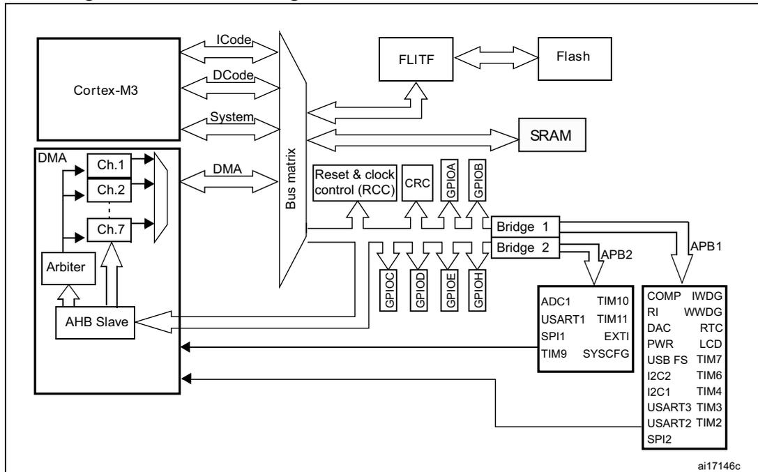
The diagram illustrates the internal architecture of STM32L1xxxx devices, focusing on the Direct Memory Access (DMA) system. At the top left is the Cortex-M3 core, which is connected to a central Bus matrix via ICode, DCode, System, and DMA interfaces. The Bus matrix also connects to FLITF (which is linked to Flash), SRAM, Reset & clock control (RCC), CRC, GPIOA, and GPIOB. Below the Bus matrix are four additional GPIO blocks: GPIOC, GPIOD, GPIOE, and GPIOH. To the left, the DMA system consists of an AHB Slave connected to an Arbiter, which in turn connects to DMA channels Ch.1, Ch.2, through Ch.7. These channels are connected to the Bus matrix. On the right, Bridge 1 and Bridge 2 connect the Bus matrix to APB1 and APB2 buses. APB1 includes peripherals: COMP, RI, WWDG, DAC, RTC, PWR, LCD, USB FS, TIM7, I2C2, TIM6, I2C1, TIM4, USART3, TIM3, USART2, TIM2, and SPI2. APB2 includes peripherals: ADC1, TIM10, USART1, TIM11, SPI1, EXTI, TIM9, and SYSCFG. The identifier 'ai17146c' is located at the bottom right of the diagram.
Figure 35. DMA block diagram in Cat.3 STM32L1xxxx devices
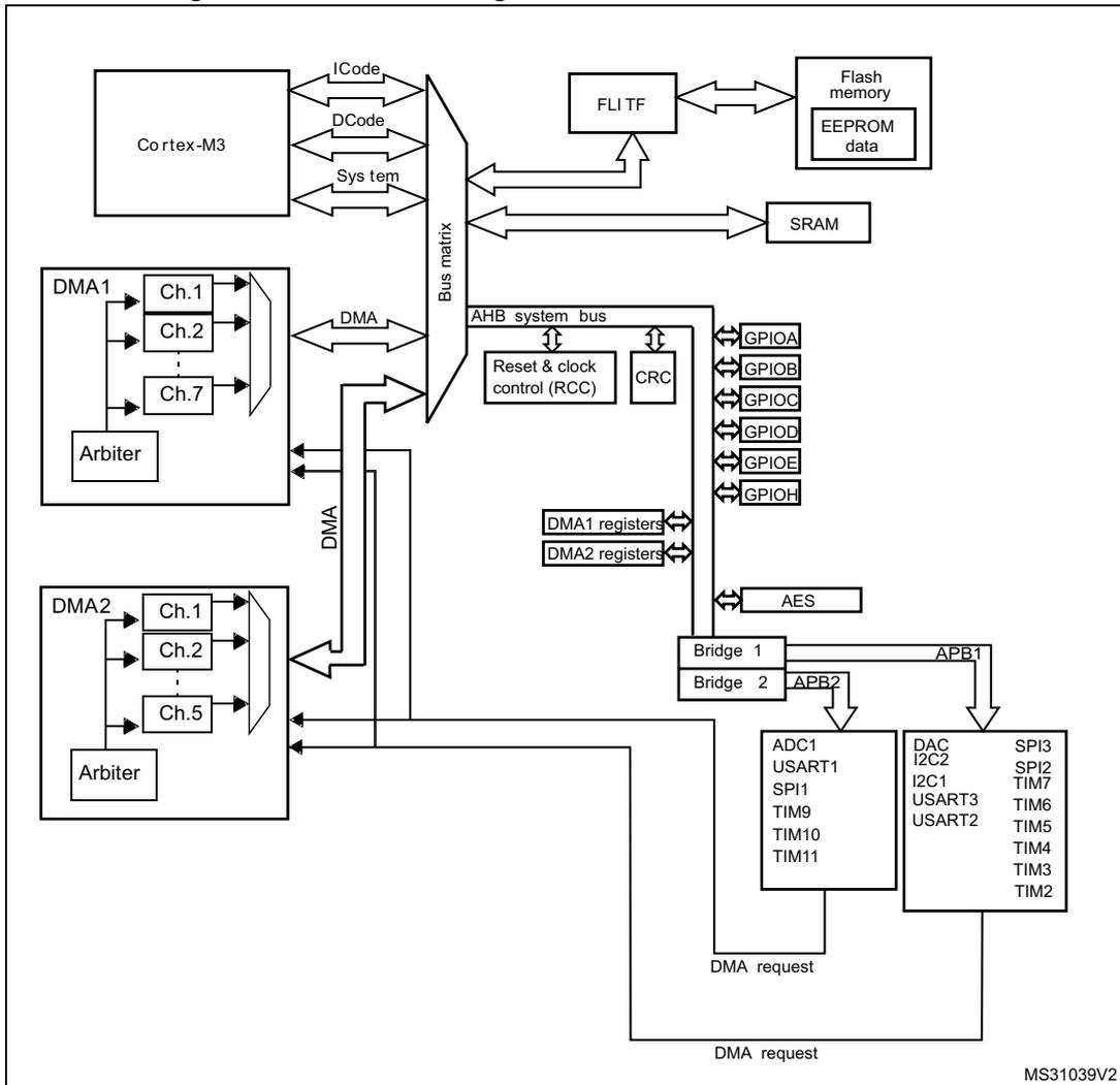
The diagram illustrates the DMA architecture in Cat.3 STM32L1xxxx devices. At the top left, the Cortex-M3 processor is connected to a Bus matrix via ICode, DCode, and System interfaces. The Bus matrix is the central hub, connecting to FLITF (which in turn connects to Flash memory and EEPROM data), SRAM, and the AHB system bus. The AHB system bus includes Reset & clock control (RCC) and CRC blocks. DMA1 and DMA2 controllers are connected to the Bus matrix. DMA1 has 7 channels (Ch.1 to Ch.7) and an Arbiter. DMA2 has 5 channels (Ch.1 to Ch.5) and an Arbiter. DMA registers for DMA1 and DMA2 are also connected to the Bus matrix. The AHB system bus connects to a group of peripherals: GPIOA through GPIOH, and AES. Below these, Bridge 1 and Bridge 2 connect to APB1 and APB2 buses. APB1 peripherals include ADC1, USART1, SPI1, TIM9, TIM10, and TIM11. APB2 peripherals include DAC, I2C2, I2C1, USART3, USART2, SPI3, SPI2, TIM7, TIM6, TIM5, TIM4, TIM3, and TIM2. DMA request lines are shown from the APB1 and APB2 peripheral groups back to the DMA controllers. The identifier MS31039V2 is located in the bottom right corner.
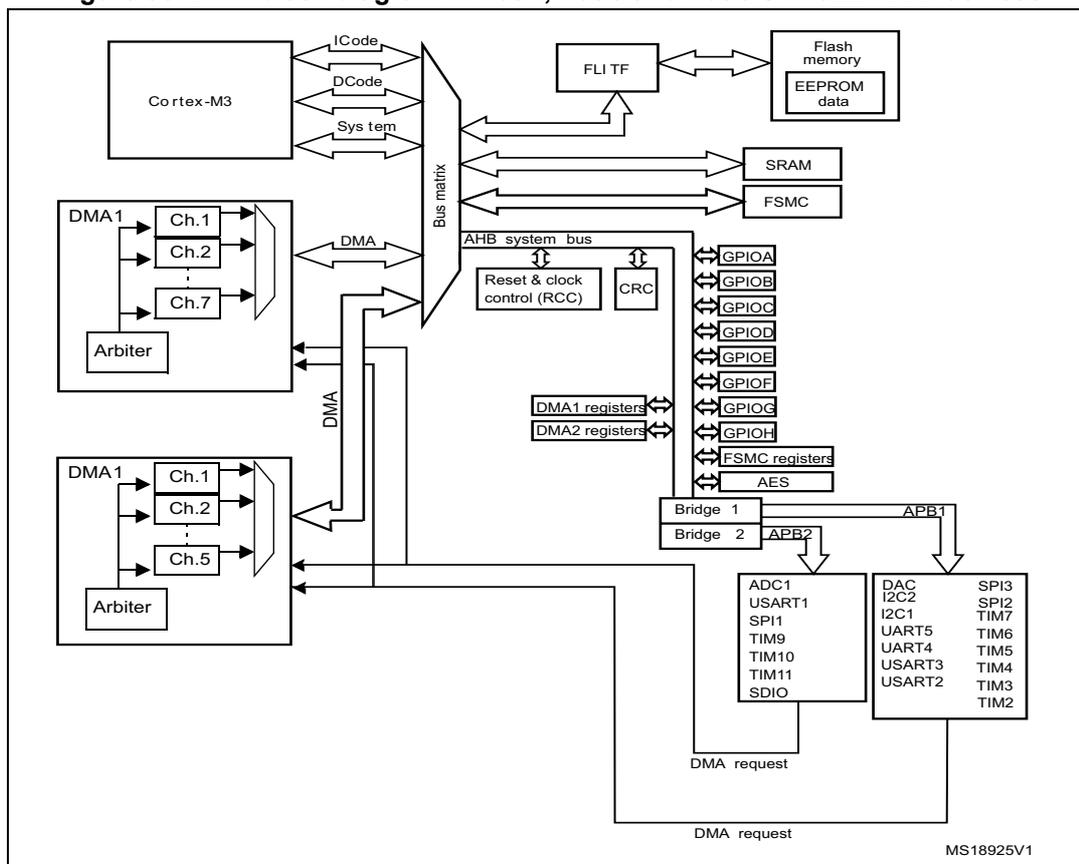
Figure 36. DMA block diagram in Cat.4, Cat.5 and Cat.6 STM32L1xxxx devices
Note:
The DMA2 controller and its related requests are available only in Cat.3, Cat.4, Cat.5 and Cat.6 devices.
SPI3 and TIM5 DMA requests are available only in Cat.3, Cat.4, Cat.5 and Cat.6 devices.
UART4 and UART5 are available only in Cat.4, Cat.5 and Cat.6 devices.
FSMC and SDIO are available only in Cat.4 devices.
11.3 DMA functional description
The DMA controller performs direct memory transfer by sharing the system bus with the Cortex ® -M3 core. The DMA request may stop the CPU access to the system bus for some bus cycles, when the CPU and DMA are targeting the same destination (memory or peripheral). The bus matrix implements round-robin scheduling, thus ensuring at least half of the system bus bandwidth (both to memory and peripheral) for the CPU.
11.3.1 DMA transactions
After an event, the peripheral sends a request signal to the DMA controller. The DMA controller serves the request depending on the channel priority. As soon as the controller accesses the peripheral, an Acknowledge is sent to the peripheral by the controller. The peripheral releases its request as soon as it gets the Acknowledge from the controller. Once the request is deasserted by the peripheral, the controller releases the Acknowledge. If there are more requests, the peripheral can initiate the next transaction.
In summary, each DMA transfer consists of three operations:
- • The loading of data from the peripheral data register or a location in memory addressed through an internal current peripheral/memory address register. The start address used for the first transfer is the base peripheral/memory address programmed in the DMA_CPARx or DMA_CMARx register
- • The storage of the data loaded to the peripheral data register or a location in memory addressed through an internal current peripheral/memory address register. The start address used for the first transfer is the base peripheral/memory address programmed in the DMA_CPARx or DMA_CMARx register
- • The post-decrementing of the DMA_CNDTRx register, which contains the number of transactions that have still to be performed.
11.3.2 Arbiter
The arbiter manages the channel requests based on their priority and launches the peripheral/memory access sequences.
The priorities are managed in two stages:
- • Software: each channel priority can be configured in the DMA_CCRx register. There are four levels:
- – Very high priority
- – High priority
- – Medium priority
- – Low priority
- • Hardware: if two requests have the same software priority level, the channel with the lowest number gets priority versus the channel with the highest number. For example, channel 2 gets priority over channel 4.
11.3.3 DMA channels
Each channel can handle DMA transfer between a peripheral register located at a fixed address and a memory address. The amount of data to be transferred (up to 65535) is programmable. The register which contains the amount of data items to be transferred is decremented after each transaction.
Programmable data sizes
Transfer data sizes of the peripheral and memory are fully programmable through the PSIZE and MSIZE bits in the DMA_CCRx register.
Pointer incrementation
Peripheral and memory pointers can optionally be automatically post-incremented after each transaction depending on the PINC and MINC bits in the DMA_CCRx register. If incremented mode is enabled, the address of the next transfer is the address of the previous one incremented by 1, 2 or 4 depending on the chosen data size. The first transfer address is the one programmed in the DMA_CPARx/DMA_CMARx registers. During transfer operations, these registers keep the initially programmed value. The current transfer addresses (in the current internal peripheral/memory address register) are not accessible by software.
If the channel is configured in non-circular mode, no DMA request is served after the last transfer (that is once the number of data items to be transferred has reached zero). In order to reload a new number of data items to be transferred into the DMA_CNDTRx register, the DMA channel must be disabled.
Note: If a DMA channel is disabled, the DMA registers are not reset. The DMA channel registers (DMA_CCRx, DMA_CPARx and DMA_CMARx) retain the initial values programmed during the channel configuration phase.
In circular mode, after the last transfer, the DMA_CNDTRx register is automatically reloaded with the initially programmed value. The current internal address registers are reloaded with the base address values from the DMA_CPARx/DMA_CMARx registers.
Channel configuration procedure
The following sequence should be followed to configure a DMA channel x (where x is the channel number).
- 1. Set the peripheral register address in the DMA_CPARx register. The data are moved from/ to this address to/ from the memory after the peripheral event.
- 2. Set the memory address in the DMA_CMARx register. The data are written to or read from this memory after the peripheral event.
- 3. Configure the total number of data to be transferred in the DMA_CNDTRx register. After each peripheral event, this value is decremented.
- 4. Configure the channel priority using the PL[1:0] bits in the DMA_CCRx register
- 5. Configure data transfer direction, circular mode, peripheral & memory incremented mode, peripheral & memory data size, and interrupt after half and/or full transfer in the DMA_CCRx register
- 6. Activate the channel by setting the ENABLE bit in the DMA_CCRx register.
As soon as the channel is enabled, it can serve any DMA request from the peripheral connected on the channel.
Once half of the bytes are transferred, the half-transfer flag (HTIF) is set and an interrupt is generated if the Half-Transfer Interrupt Enable bit (HTIE) is set. At the end of the transfer, the Transfer Complete Flag (TCIF) is set and an interrupt is generated if the Transfer Complete Interrupt Enable bit (TCIE) is set.
Circular mode
Circular mode is available to handle circular buffers and continuous data flows (e.g. ADC scan mode). This feature can be enabled using the CIRC bit in the DMA_CCRx register. When circular mode is activated, the number of data to be transferred is automatically reloaded with the initial value programmed during the channel configuration phase, and the DMA requests continue to be served.
Memory-to-memory mode
The DMA channels can also work without being triggered by a request from a peripheral. This mode is called Memory to Memory mode.
If the MEM2MEM bit in the DMA_CCRx register is set, then the channel initiates transfers as soon as it is enabled by software by setting the Enable bit (EN) in the DMA_CCRx register. The transfer stops once the DMA_CNDTRx register reaches zero. Memory to Memory mode may not be used at the same time as Circular mode.
11.3.4 Programmable data width, data alignment and endians
When PSIZE and MSIZE are not equal, the DMA performs some data alignments as described in Table 53 .
Table 53. Programmable data width and endian behavior (when bits PINC = MINC = 1)
| Source port width | Destination port width | Number of data items to transfer (NDT) | Source content: address / data | Transfer operations | Destination content: address / data |
|---|---|---|---|---|---|
| 8 | 8 | 4 | @0x0 / B0 @0x1 / B1 @0x2 / B2 @0x3 / B3 | 1: READ B0[7:0] @0x0 then WRITE B0[7:0] @0x0 2: READ B1[7:0] @0x1 then WRITE B1[7:0] @0x1 3: READ B2[7:0] @0x2 then WRITE B2[7:0] @0x2 4: READ B3[7:0] @0x3 then WRITE B3[7:0] @0x3 | @0x0 / B0 @0x1 / B1 @0x2 / B2 @0x3 / B3 |
| 8 | 16 | 4 | @0x0 / B0 @0x1 / B1 @0x2 / B2 @0x3 / B3 | 1: READ B0[7:0] @0x0 then WRITE 00B0[15:0] @0x0 2: READ B1[7:0] @0x1 then WRITE 00B1[15:0] @0x2 3: READ B3[7:0] @0x2 then WRITE 00B2[15:0] @0x4 4: READ B4[7:0] @0x3 then WRITE 00B3[15:0] @0x6 | @0x0 / 00B0 @0x2 / 00B1 @0x4 / 00B2 @0x6 / 00B3 |
| 8 | 32 | 4 | @0x0 / B0 @0x1 / B1 @0x2 / B2 @0x3 / B3 | 1: READ B0[7:0] @0x0 then WRITE 000000B0[31:0] @0x0 2: READ B1[7:0] @0x1 then WRITE 000000B1[31:0] @0x4 3: READ B3[7:0] @0x2 then WRITE 000000B2[31:0] @0x8 4: READ B4[7:0] @0x3 then WRITE 000000B3[31:0] @0xC | @0x0 / 000000B0 @0x4 / 000000B1 @0x8 / 000000B2 @0xC / 000000B3 |
| 16 | 8 | 4 | @0x0 / B1B0 @0x2 / B3B2 @0x4 / B5B4 @0x6 / B7B6 | 1: READ B1B0[15:0] @0x0 then WRITE B0[7:0] @0x0 2: READ B3B2[15:0] @0x2 then WRITE B2[7:0] @0x1 3: READ B5B4[15:0] @0x4 then WRITE B4[7:0] @0x2 4: READ B7B6[15:0] @0x6 then WRITE B6[7:0] @0x3 | @0x0 / B0 @0x1 / B2 @0x2 / B4 @0x3 / B6 |
| 16 | 16 | 4 | @0x0 / B1B0 @0x2 / B3B2 @0x4 / B5B4 @0x6 / B7B6 | 1: READ B1B0[15:0] @0x0 then WRITE B1B0[15:0] @0x0 2: READ B3B2[15:0] @0x2 then WRITE B3B2[15:0] @0x2 3: READ B5B4[15:0] @0x4 then WRITE B5B4[15:0] @0x4 4: READ B7B6[15:0] @0x6 then WRITE B7B6[15:0] @0x6 | @0x0 / B1B0 @0x2 / B3B2 @0x4 / B5B4 @0x6 / B7B6 |
| 16 | 32 | 4 | @0x0 / B1B0 @0x2 / B3B2 @0x4 / B5B4 @0x6 / B7B6 | 1: READ B1B0[15:0] @0x0 then WRITE 0000B1B0[31:0] @0x0 2: READ B3B2[15:0] @0x2 then WRITE 0000B3B2[31:0] @0x4 3: READ B5B4[15:0] @0x4 then WRITE 0000B5B4[31:0] @0x8 4: READ B7B6[15:0] @0x6 then WRITE 0000B7B6[31:0] @0xC | @0x0 / 0000B1B0 @0x4 / 0000B3B2 @0x8 / 0000B5B4 @0xC / 0000B7B6 |
| 32 | 8 | 4 | @0x0 / B3B2B1B0 @0x4 / B7B6B5B4 @0x8 / BBBAB9B8 @0xC / BFBEBDBC | 1: READ B3B2B1B0[31:0] @0x0 then WRITE B0[7:0] @0x0 2: READ B7B6B5B4[31:0] @0x4 then WRITE B4[7:0] @0x1 3: READ BBBAB9B8[31:0] @0x8 then WRITE B8[7:0] @0x2 4: READ BFBEBDBC[31:0] @0xC then WRITE BC[7:0] @0x3 | @0x0 / B0 @0x1 / B4 @0x2 / B8 @0x3 / BC |
| 32 | 16 | 4 | @0x0 / B3B2B1B0 @0x4 / B7B6B5B4 @0x8 / BBBAB9B8 @0xC / BFBEBDBC | 1: READ B3B2B1B0[31:0] @0x0 then WRITE B1B0[7:0] @0x0 2: READ B7B6B5B4[31:0] @0x4 then WRITE B5B4[7:0] @0x1 3: READ BBBAB9B8[31:0] @0x8 then WRITE B9B8[7:0] @0x2 4: READ BFBEBDBC[31:0] @0xC then WRITE BDBC[7:0] @0x3 | @0x0 / B1B0 @0x2 / B5B4 @0x4 / B9B8 @0x6 / BDBC |
| 32 | 32 | 4 | @0x0 / B3B2B1B0 @0x4 / B7B6B5B4 @0x8 / BBBAB9B8 @0xC / BFBEBDBC | 1: READ B3B2B1B0[31:0] @0x0 then WRITE B3B2B1B0[31:0] @0x0 2: READ B7B6B5B4[31:0] @0x4 then WRITE B7B6B5B4[31:0] @0x4 3: READ BBBAB9B8[31:0] @0x8 then WRITE BBBAB9B8[31:0] @0x8 4: READ BFBEBDBC[31:0] @0xC then WRITE BFBEBDBC[31:0] @0xC | @0x0 / B3B2B1B0 @0x4 / B7B6B5B4 @0x8 / BBBAB9B8 @0xC / BFBEBDBC |
Addressing an AHB peripheral that does not support byte or halfword write operations
When the DMA initiates an AHB byte or halfword write operation, the data are duplicated on the unused lanes of the HWDATA[31:0] bus. So when the used AHB slave peripheral does not support byte or halfword write operations (when HSIZE is not used by the peripheral)
and does not generate any error, the DMA writes the 32 HWDATA bits as shown in the two examples below:
- • To write the halfword “0xABCD”, the DMA sets the HWDATA bus to “0xABCDABCD” with HSIZE = HalfWord
- • To write the byte “0xAB”, the DMA sets the HWDATA bus to “0xABABABAB” with HSIZE = Byte
Assuming that the AHB/APB bridge is an AHB 32-bit slave peripheral that does not take the HSIZE data into account, it transforms any AHB byte or halfword operation into a 32-bit APB operation in the following manner:
- • an AHB byte write operation of the data “0xB0” to 0x0 (or to 0x1, 0x2 or 0x3) is converted to an APB word write operation of the data “0xB0B0B0B0” to 0x0
- • an AHB halfword write operation of the data “0xB1B0” to 0x0 (or to 0x2) is converted to an APB word write operation of the data “0xB1B0B1B0” to 0x0
For instance, to write the APB backup registers (16-bit registers aligned to a 32-bit address boundary), the memory source size (MSIZE) must be configured to “16-bit” and the peripheral destination size (PSIZE) to “32-bit”.
11.3.5 Error management
A DMA transfer error can be generated by reading from or writing to a reserved address space. When a DMA transfer error occurs during a DMA read or a write access, the faulty channel is automatically disabled through a hardware clear of its EN bit in the corresponding Channel configuration register (DMA_CCRx). The channel's transfer error interrupt flag (TEIF) in the DMA_IFR register is set and an interrupt is generated if the transfer error interrupt enable bit (TEIE) in the DMA_CCRx register is set.
11.3.6 Interrupts
An interrupt can be produced on a Half-transfer, Transfer complete or Transfer error for each DMA channel. Separate interrupt enable bits are available for flexibility.
Table 54. DMA interrupt requests
| Interrupt event | Event flag | Enable Control bit |
|---|---|---|
| Half-transfer | HTIF | HTIE |
| Transfer complete | TCIF | TCIE |
| Transfer error | TEIF | TEIE |
11.3.7 DMA request mapping
DMA1 controller
The 7 requests from the peripherals (TIMx[2,3,4,6,7], ADC1, SPI[1,2], I2Cx[1,2], USARTx[1,2,3]) and DAC Channelx[1,2] are simply logically ORed before entering the DMA1, this means that only one request must be enabled at a time. Refer to Figure 37 .
The peripheral DMA requests can be independently activated/de-activated by programming the DMA control bit in the registers of the corresponding peripheral.
Figure 37. DMA1 request mapping
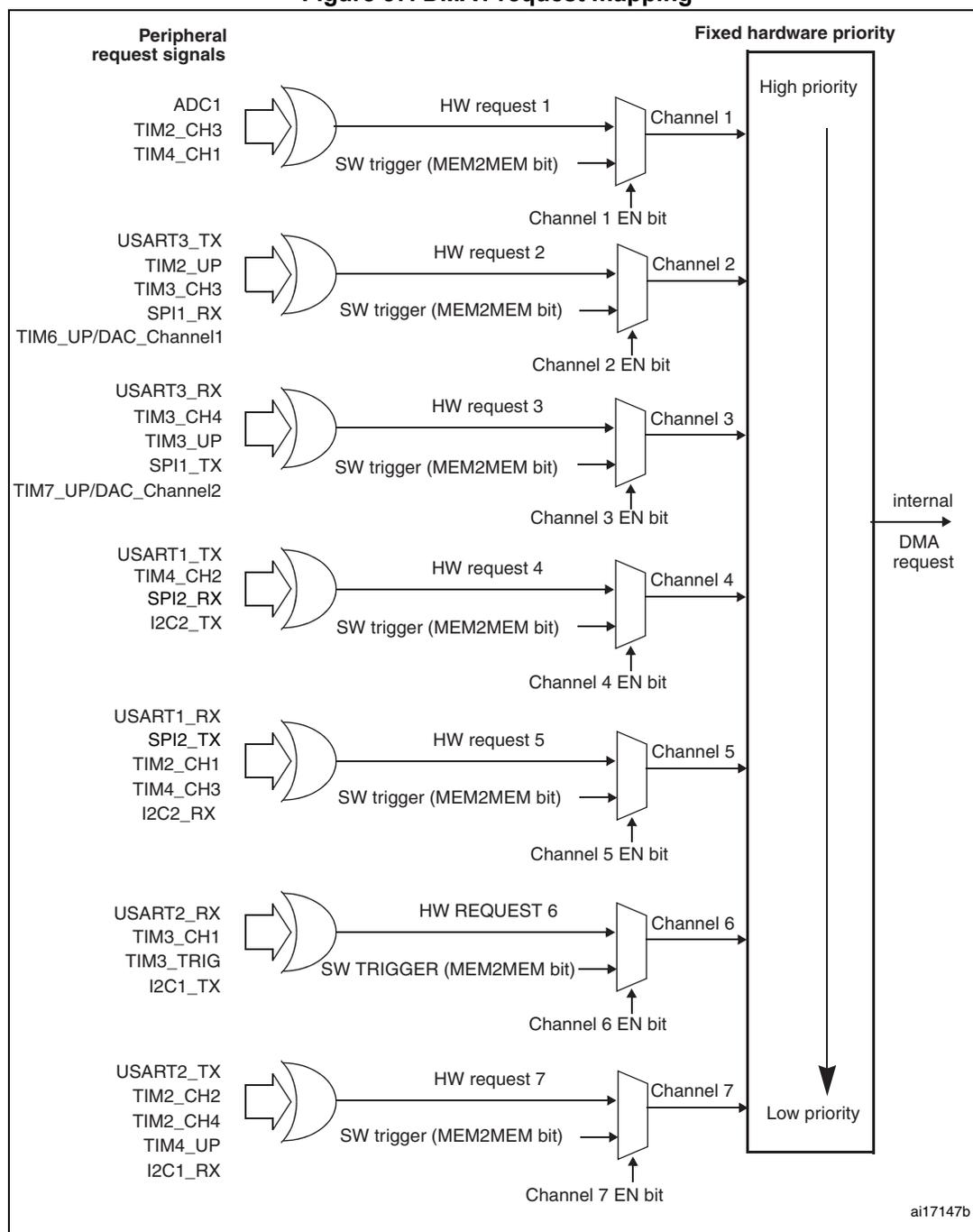
The diagram illustrates the mapping of peripheral request signals to DMA1 channels. Each channel is associated with specific peripheral signals, a hardware request line, and a software trigger. The channels are prioritized from High priority (Channel 1) to Low priority (Channel 7). Each channel has an Enable (EN) bit.
| Channel | Peripheral request signals | HW request | SW trigger (MEM2MEM bit) | EN bit |
|---|---|---|---|---|
| Channel 1 | ADC1, TIM2_CH3, TIM4_CH1 | HW request 1 | SW trigger (MEM2MEM bit) | Channel 1 EN bit |
| Channel 2 | USART3_TX, TIM2_UP, TIM3_CH3, SPI1_RX, TIM6_UP/DAC_Channel1 | HW request 2 | SW trigger (MEM2MEM bit) | Channel 2 EN bit |
| Channel 3 | USART3_RX, TIM3_CH4, TIM3_UP, SPI1_TX, TIM7_UP/DAC_Channel2 | HW request 3 | SW trigger (MEM2MEM bit) | Channel 3 EN bit |
| Channel 4 | USART1_TX, TIM4_CH2, SPI2_RX, I2C2_TX | HW request 4 | SW trigger (MEM2MEM bit) | Channel 4 EN bit |
| Channel 5 | USART1_RX, SPI2_TX, TIM2_CH1, TIM4_CH3, I2C2_RX | HW request 5 | SW trigger (MEM2MEM bit) | Channel 5 EN bit |
| Channel 6 | USART2_RX, TIM3_CH1, TIM3_TRIG, I2C1_TX | HW REQUEST 6 | SW TRIGGER (MEM2MEM bit) | Channel 6 EN bit |
| Channel 7 | USART2_TX, TIM2_CH2, TIM2_CH4, TIM4_UP, I2C1_RX | HW request 7 | SW trigger (MEM2MEM bit) | Channel 7 EN bit |
Fixed hardware priority: High priority (top) to Low priority (bottom). The internal DMA request is generated by the combination of hardware and software triggers for each channel.
Table 55 lists the DMA requests for each channel.
Table 55. Summary of DMA1 requests for each channel
| Peripherals | Channel 1 | Channel 2 | Channel 3 | Channel 4 | Channel 5 | Channel 6 | Channel 7 |
|---|---|---|---|---|---|---|---|
| ADC1 | ADC1 | - | - | - | - | - | - |
| SPI | - | SPI1_RX | SPI1_TX | SPI2_RX | SPI2_TX | - | - |
| USART | - | USART3_TX | USART3_RX | USART1_TX | USART1_RX | USART2_RX | USART2_TX |
| I 2 C | - | - | - | I2C2_TX | I2C2_RX | I2C1_TX | I2C1_RX |
| TIM2 | TIM2_CH3 | TIM2_UP | - | - | TIM2_CH1 | - | TIM2_CH2 TIM2_CH4 |
| TIM3 | - | TIM3_CH3 | TIM3_CH4 TIM3_UP | - | - | TIM3_CH1 TIM3_TRIG | - |
| TIM4 | TIM4_CH1 | - | - | TIM4_CH2 | TIM4_CH3 | - | TIM4_UP |
| TIM6/DAC_ Channel1 | - | TIM6_UP/DA C_Channel1 | - | - | - | - | - |
| TIM7/DAC_ Channel2 | - | - | TIM7_UP/DA C_Channel2 | - | - | - | - |
Figure 38. DMA2 request mapping
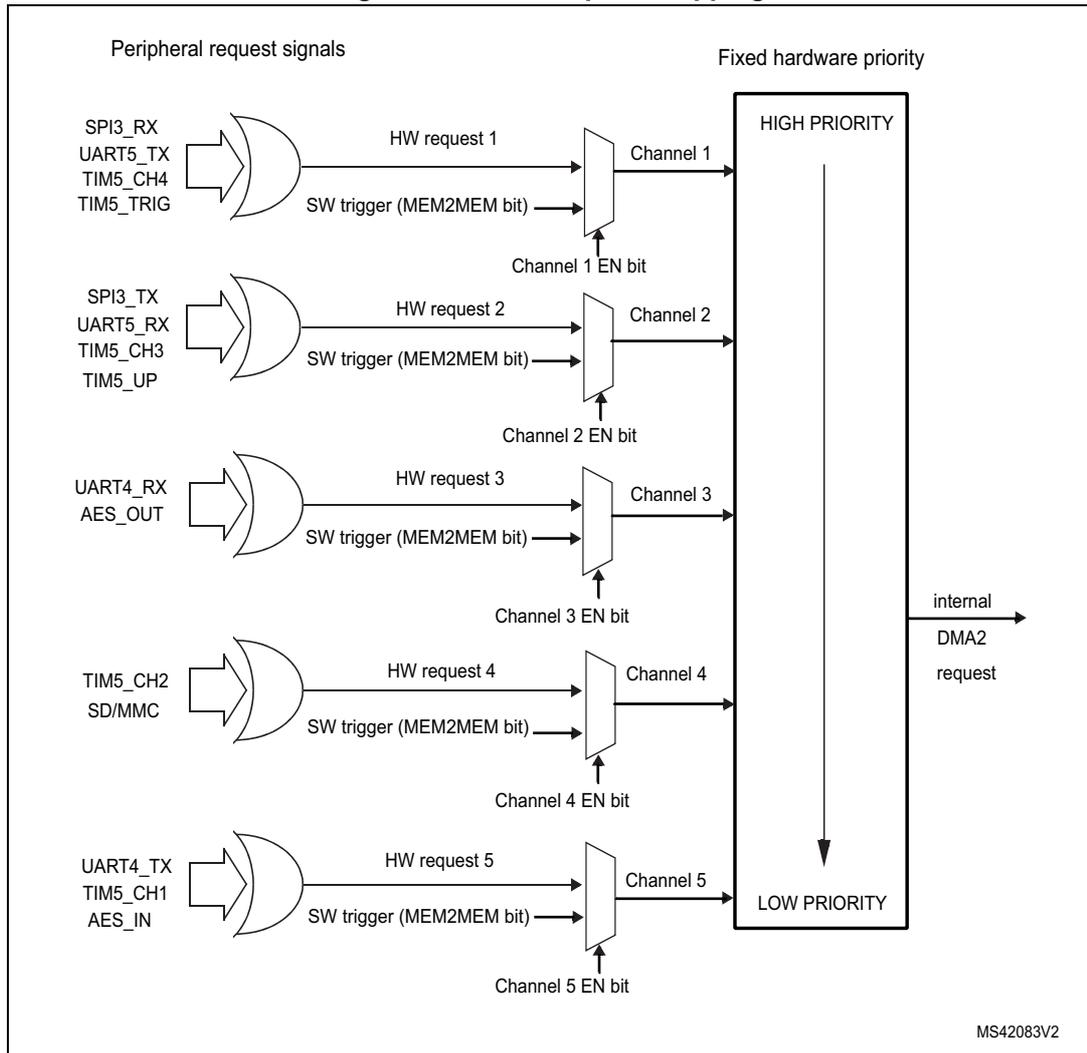
The diagram illustrates the DMA2 request mapping for five channels. Each channel is associated with specific peripheral request signals and a hardware request line. The channels are prioritized from HIGH PRIORITY at the top to LOW PRIORITY at the bottom. Each channel has an enable (EN) bit and a software trigger (MEM2MEM bit). The internal DMA2 request is generated based on the priority and enable status of the channels.
| Channel | Peripheral Request Signals | HW Request | SW Trigger (MEM2MEM bit) | EN bit |
|---|---|---|---|---|
| Channel 1 | SPI3_RX, UART5_TX, TIM5_CH4, TIM5_TRIG | HW request 1 | SW trigger (MEM2MEM bit) | Channel 1 EN bit |
| Channel 2 | SPI3_TX, UART5_RX, TIM5_CH3, TIM5_UP | HW request 2 | SW trigger (MEM2MEM bit) | Channel 2 EN bit |
| Channel 3 | UART4_RX, AES_OUT | HW request 3 | SW trigger (MEM2MEM bit) | Channel 3 EN bit |
| Channel 4 | TIM5_CH2, SD/MMC | HW request 4 | SW trigger (MEM2MEM bit) | Channel 4 EN bit |
| Channel 5 | UART4_TX, TIM5_CH1, AES_IN | HW request 5 | SW trigger (MEM2MEM bit) | Channel 5 EN bit |
Table 56 lists the DMA2 requests for each channel.
Table 56. Summary of DMA2 requests for each channel
| Peripherals | Channel 1 | Channel 2 | Channel 3 | Channel 4 | Channel 5 |
|---|---|---|---|---|---|
| SPI3 | SPI3_RX | SPI3_TX | - | - | - |
| UART4 | - | - | UART4_RX | - | UART4_TX |
| UART5 | UART5_TX | UART5_RX | - | - | - |
| TIM5 | TIM5_CH4 TIM5_TRIG | TIM5_CH3 TIM5_UP | - | TIM5_CH2 | TIM5_CH1 |
| SDIO | - | - | - | SD/MMC | - |
| AES | - | - | AES_OUT | - | AES_IN |
11.4 DMA registers
Refer to Section 1.2: List of abbreviations for registers on page 38 for a list of abbreviations used in register descriptions.
Note: In the following registers, all bits related to channel6 and channel7 are not relevant for DMA2 since it has only 5 channels.
The peripheral registers can be accessed by bytes (8-bit), half-words (16-bit) or words (32-bit).
11.4.1 DMA interrupt status register (DMA_ISR)
Address offset: 0x00
Reset value: 0x0000 0000
| 31 | 30 | 29 | 28 | 27 | 26 | 25 | 24 | 23 | 22 | 21 | 20 | 19 | 18 | 17 | 16 |
|---|---|---|---|---|---|---|---|---|---|---|---|---|---|---|---|
| Reserved | TEIF7 | HTIF7 | TCIF7 | GIF7 | TEIF6 | HTIF6 | TCIF6 | GIF6 | TEIF5 | HTIF5 | TCIF5 | GIF5 | |||
| 15 | 14 | 13 | 12 | 11 | 10 | 9 | 8 | 7 | 6 | 5 | 4 | 3 | 2 | 1 | 0 |
| TEIF4 | HTIF4 | TCIF4 | GIF4 | TEIF3 | HTIF3 | TCIF3 | GIF3 | TEIF2 | HTIF2 | TCIF2 | GIF2 | TEIF1 | HTIF1 | TCIF1 | GIF1 |
| r | r | r | r | r | r | r | r | r | r | r | r | r | r | r | r |
Bits 31:28 Reserved, must be kept at reset value.
Bits 27, 23, 19, 15, TEIFx : Channel x transfer error flag (x = 1 ..7)
11, 7, 3 This bit is set by hardware. It is cleared by software writing 1 to the corresponding bit in the DMA_IFCR register.
0: No transfer error (TE) on channel x
1: A transfer error (TE) occurred on channel x
Bits 26, 22, 18, 14, HTIFx : Channel x half transfer flag (x = 1 ..7)
10, 6, 2 This bit is set by hardware. It is cleared by software writing 1 to the corresponding bit in the DMA_IFCR register.
0: No half transfer (HT) event on channel x
1: A half transfer (HT) event occurred on channel x
Bits 25, 21, 17, 13, TCIFx : Channel x transfer complete flag (x = 1 ..7)
9, 5, 1 This bit is set by hardware. It is cleared by software writing 1 to the corresponding bit in the DMA_IFCR register.
0: No transfer complete (TC) event on channel x
1: A transfer complete (TC) event occurred on channel x
Bits 24, 20, 16, 12, GIFx : Channel x global interrupt flag (x = 1 ..7)
8, 4, 0 This bit is set by hardware. It is cleared by software writing 1 to the corresponding bit in the DMA_IFCR register.
0: No TE, HT or TC event on channel x
1: A TE, HT or TC event occurred on channel x
11.4.2 DMA interrupt flag clear register (DMA_IFCR)
Address offset: 0x04
Reset value: 0x0000 0000
| 31 | 30 | 29 | 28 | 27 | 26 | 25 | 24 | 23 | 22 | 21 | 20 | 19 | 18 | 17 | 16 |
|---|---|---|---|---|---|---|---|---|---|---|---|---|---|---|---|
| Reserved | CTEIF 7 | CHTIF 7 | CTCIF7 | CGIF7 | CTEIF6 | CHTIF6 | CTCIF6 | CGIF6 | CTEIF5 | CHTIF5 | CTCIF5 | ||||
| w | w | w | w | w | w | w | w | w | w | w | |||||
| 15 | 14 | 13 | 12 | 11 | 10 | 9 | 8 | 7 | 6 | 5 | 4 | 3 | 2 | 1 | 0 |
| CTEIF 4 | CHTIF 4 | CTCIF 4 | CGIF4 | CTEIF 3 | CHTIF 3 | CTCIF3 | CGIF3 | CTEIF2 | CHTIF2 | CTCIF2 | CGIF2 | CTEIF1 | CHTIF1 | CTCIF1 | CGIF1 |
| w | w | w | w | w | w | w | w | w | w | w | w | w | w | w | w |
Bits 31:28 Reserved, must be kept at reset value.
Bits 27, 23, 19, 15, CTEIFx : Channel x transfer error clear (x = 1 ..7)
11, 7, 3 This bit is set and cleared by software.
0: No effect
1: Clears the corresponding TEIF flag in the DMA_ISR register
Bits 26, 22, 18, 14, CHTIFx : Channel x half transfer clear (x = 1 ..7)
10, 6, 2 This bit is set and cleared by software.
0: No effect
1: Clears the corresponding HTIF flag in the DMA_ISR register
Bits 25, 21, 17, 13, CTCIFx : Channel x transfer complete clear (x = 1 ..7)
9, 5, 1 This bit is set and cleared by software.
0: No effect
1: Clears the corresponding TCIF flag in the DMA_ISR register
Bits 24, 20, 16, 12, CGIFx : Channel x global interrupt clear (x = 1 ..7)
8, 4, 0 This bit is set and cleared by software.
0: No effect
1: Clears the GIF, TEIF, HTIF and TCIF flags in the DMA_ISR register
11.4.3 DMA channel x configuration register (DMA_CCRx) (x = 1..7, where x = channel number)
Address offset: 0x08 + 0d20 × (channel number – 1)
Reset value: 0x0000 0000
| 31 | 30 | 29 | 28 | 27 | 26 | 25 | 24 | 23 | 22 | 21 | 20 | 19 | 18 | 17 | 16 |
|---|---|---|---|---|---|---|---|---|---|---|---|---|---|---|---|
| Reserved | |||||||||||||||
| 15 | 14 | 13 | 12 | 11 | 10 | 9 | 8 | 7 | 6 | 5 | 4 | 3 | 2 | 1 | 0 |
| Res. | MEM2 MEM | PL[1:0] | MSIZE[1:0] | PSIZE[1:0] | MINC | PINC | CIRC | DIR | TEIE | HTIE | TCIE | EN | |||
| rw | rw | rw | rw | rw | rw | rw | rw | rw | rw | rw | rw | rw | rw | rw | |
Bits 31:15 Reserved, must be kept at reset value.
Bit 14 MEM2MEM : Memory to memory mode
This bit is set and cleared by software.
0: Memory to memory mode disabled
1: Memory to memory mode enabled
Bits 13:12 PL[1:0] : Channel priority level
These bits are set and cleared by software.
00: Low
01: Medium
10: High
11: Very high
Bits 11:10 MSIZE[1:0] : Memory size
These bits are set and cleared by software.
00: 8-bits
01: 16-bits
10: 32-bits
11: Reserved
Bits 9:8 PSIZE[1:0] : Peripheral size
These bits are set and cleared by software.
00: 8-bits
01: 16-bits
10: 32-bits
11: Reserved
Bit 7 MINC : Memory increment mode
This bit is set and cleared by software.
0: Memory increment mode disabled
1: Memory increment mode enabled
Bit 6 PINC : Peripheral increment mode
This bit is set and cleared by software.
0: Peripheral increment mode disabled
1: Peripheral increment mode enabled
Bit 5 CIRC : Circular mode
This bit is set and cleared by software.
0: Circular mode disabled
1: Circular mode enabled
Bit 4 DIR : Data transfer direction
This bit is set and cleared by software.
0: Read from peripheral
1: Read from memory
Bit 3 TEIE : Transfer error interrupt enable
This bit is set and cleared by software.
0: TE interrupt disabled
1: TE interrupt enabled
Bit 2 HTIE : Half transfer interrupt enable
This bit is set and cleared by software.
0: HT interrupt disabled
1: HT interrupt enabled
Bit 1 TCIE : Transfer complete interrupt enable
This bit is set and cleared by software.
0: TC interrupt disabled
1: TC interrupt enabled
Bit 0 EN : Channel enable
This bit is set and cleared by software.
0: Channel disabled
1: Channel enabled
11.4.4 DMA channel x number of data register (DMA_CNDTRx) (x = 1..7, where x = channel number)
Address offset: 0x0C + 0d20 × (channel number – 1)
Reset value: 0x0000 0000
| 31 | 30 | 29 | 28 | 27 | 26 | 25 | 24 | 23 | 22 | 21 | 20 | 19 | 18 | 17 | 16 |
|---|---|---|---|---|---|---|---|---|---|---|---|---|---|---|---|
| Reserved | |||||||||||||||
| 15 | 14 | 13 | 12 | 11 | 10 | 9 | 8 | 7 | 6 | 5 | 4 | 3 | 2 | 1 | 0 |
| NDT | |||||||||||||||
| rw | rw | rw | rw | rw | rw | rw | rw | rw | rw | rw | rw | rw | rw | rw | rw |
Bits 31:16 Reserved, must be kept at reset value.
Bits 15:0 NDT[15:0] : Number of data to transfer
Number of data to be transferred (0 up to 65535). This register can only be written when the channel is disabled. Once the channel is enabled, this register is read-only, indicating the remaining bytes to be transmitted. This register decrements after each DMA transfer.
Once the transfer is completed, this register can either stay at zero or be reloaded automatically by the value previously programmed if the channel is configured in auto-reload mode.
If this register is zero, no transaction can be served whether the channel is enabled or not.
11.4.5 DMA channel x peripheral address register (DMA_CPARx) (x = 1..7, where x = channel number)
Address offset: \( 0x10 + 0d20 \times (\text{channel number} - 1) \)
Reset value: 0x0000 0000
This register must not be written when the channel is enabled.

| 31 | 30 | 29 | 28 | 27 | 26 | 25 | 24 | 23 | 22 | 21 | 20 | 19 | 18 | 17 | 16 | 15 | 14 | 13 | 12 | 11 | 10 | 9 | 8 | 7 | 6 | 5 | 4 | 3 | 2 | 1 | 0 |
| PA | |||||||||||||||||||||||||||||||
| rw | rw | rw | rw | rw | rw | rw | rw | rw | rw | rw | rw | rw | rw | rw | rw | rw | rw | rw | rw | rw | rw | rw | rw | rw | rw | rw | rw | rw | rw | rw | rw |
Bits 31:0 PA[31:0] : Peripheral address
Base address of the peripheral data register from/to which the data are read/written.
When PSIZE is 01 (16-bit), the PA[0] bit is ignored. Access is automatically aligned to a half-word address.
When PSIZE is 10 (32-bit), PA[1:0] are ignored. Access is automatically aligned to a word address.
11.4.6 DMA channel x memory address register (DMA_CMARx) (x = 1..7, where x = channel number)
Address offset: \( 0x14 + 0d20 \times (\text{channel number} - 1) \)
Reset value: 0x0000 0000
This register must not be written when the channel is enabled.

| 31 | 30 | 29 | 28 | 27 | 26 | 25 | 24 | 23 | 22 | 21 | 20 | 19 | 18 | 17 | 16 | 15 | 14 | 13 | 12 | 11 | 10 | 9 | 8 | 7 | 6 | 5 | 4 | 3 | 2 | 1 | 0 |
| MA | |||||||||||||||||||||||||||||||
| rw | rw | rw | rw | rw | rw | rw | rw | rw | rw | rw | rw | rw | rw | rw | rw | rw | rw | rw | rw | rw | rw | rw | rw | rw | rw | rw | rw | rw | rw | rw | rw |
Bits 31:0 MA[31:0] : Memory address
Base address of the memory area from/to which the data are read/written.
When MSIZE is 01 (16-bit), the MA[0] bit is ignored. Access is automatically aligned to a half-word address.
When MSIZE is 10 (32-bit), MA[1:0] are ignored. Access is automatically aligned to a word address.
11.4.7 DMA register map
The following table gives the DMA register map and the reset values. The reserved memory areas are highlighted in gray in the table.
Table 57. DMA register map and reset values
| Offset | Register | 31 | 30 | 29 | 28 | 27 | 26 | 25 | 24 | 23 | 22 | 21 | 20 | 19 | 18 | 17 | 16 | 15 | 14 | 13 | 12 | 11 | 10 | 9 | 8 | 7 | 6 | 5 | 4 | 3 | 2 | 1 | 0 |
|---|---|---|---|---|---|---|---|---|---|---|---|---|---|---|---|---|---|---|---|---|---|---|---|---|---|---|---|---|---|---|---|---|---|
| 0x000 | DMA_ISR | Reserved | TEIF7 | HTIF7 | TCIF7 | GIF7 | TEIF6 | HTIF6 | TCIF6 | GIF6 | TEIF5 | HTIF5 | TCIF5 | GIF5 | TEIF4 | HTIF4 | TCIF4 | GIF4 | TEIF3 | HTIF3 | TCIF3 | GIF3 | TEIF2 | HTIF2 | TCIF2 | GIF2 | TEIF1 | HTIF1 | TCIF1 | GIF1 | |||
| Reset value | 0 | 0 | 0 | 0 | 0 | 0 | 0 | 0 | 0 | 0 | 0 | 0 | 0 | 0 | 0 | 0 | 0 | 0 | 0 | 0 | 0 | 0 | 0 | 0 | 0 | 0 | 0 | 0 | |||||
| 0x004 | DMA_IFCR | Reserved | CTEIF7 | CHIF7 | CTCIF7 | CGIF7 | CTEIF6 | CHIF6 | CTCIF6 | CGIF6 | CTEIF5 | CHIF5 | CTCIF5 | CGIF5 | CTEIF4 | CHIF4 | CTCIF4 | CGIF4 | CTEIF3 | CHIF3 | CTCIF3 | CGIF3 | CTEIF2 | CHIF2 | CTCIF2 | CGIF2 | CTEIF1 | CHIF1 | CTCIF1 | CGIF1 | |||
| Reset value | 0 | 0 | 0 | 0 | 0 | 0 | 0 | 0 | 0 | 0 | 0 | 0 | 0 | 0 | 0 | 0 | 0 | 0 | 0 | 0 | 0 | 0 | 0 | 0 | 0 | 0 | 0 | 0 | |||||
| 0x008 | DMA_CCR1 | Reserved | MEM2MEM | PL [1:0] | M SIZE [1:0] | PSIZE [1:0] | MINC | PINC | CIRC | DIR | TEIE | HTIE | TCIE | EN | |||||||||||||||||||
| Reset value | 0 | 0 | 0 | 0 | 0 | 0 | 0 | 0 | 0 | 0 | 0 | 0 | 0 | 0 | |||||||||||||||||||
| 0x00C | DMA_CNDTR1 | Reserved | NDT[15:0] | ||||||||||||||||||||||||||||||
| Reset value | 0 | ||||||||||||||||||||||||||||||||
| 0x010 | DMA_CPAR1 | PA[31:0] | |||||||||||||||||||||||||||||||
| Reset value | |||||||||||||||||||||||||||||||||
| 0x014 | DMA_CMAR1 | MA[31:0] | |||||||||||||||||||||||||||||||
| Reset value | |||||||||||||||||||||||||||||||||
| 0x018 | Reserved | ||||||||||||||||||||||||||||||||
| 0x01C | DMA_CCR2 | Reserved | MEM2MEM | PL [1:0] | M SIZE [1:0] | PSIZE [1:0] | MINC | PINC | CIRC | DIR | TEIE | HTIE | TCIE | EN | |||||||||||||||||||
| Reset value | 0 | 0 | 0 | 0 | 0 | 0 | 0 | 0 | 0 | 0 | 0 | 0 | 0 | 0 | |||||||||||||||||||
| 0x020 | DMA_CNDTR2 | Reserved | NDT[15:0] | ||||||||||||||||||||||||||||||
| Reset value | 0 | ||||||||||||||||||||||||||||||||
| 0x024 | DMA_CPAR2 | PA[31:0] | |||||||||||||||||||||||||||||||
| Reset value | |||||||||||||||||||||||||||||||||
| 0x028 | DMA_CMAR2 | MA[31:0] | |||||||||||||||||||||||||||||||
| Reset value | |||||||||||||||||||||||||||||||||
| 0x02C | Reserved | ||||||||||||||||||||||||||||||||
| 0x030 | DMA_CCR3 | Reserved | MEM2MEM | PL [1:0] | M SIZE [1:0] | PSIZE [1:0] | MINC | PINC | CIRC | DIR | TEIE | HTIE | TCIE | EN | |||||||||||||||||||
| Reset value | 0 | 0 | 0 | 0 | 0 | 0 | 0 | 0 | 0 | 0 | 0 | 0 | 0 | 0 | |||||||||||||||||||
| 0x034 | DMA_CNDTR3 | Reserved | NDT[15:0] | ||||||||||||||||||||||||||||||
| Reset value | 0 | ||||||||||||||||||||||||||||||||
| 0x038 | DMA_CPAR3 | PA[31:0] | |||||||||||||||||||||||||||||||
| Reset value | |||||||||||||||||||||||||||||||||
| 0x03C | DMA_CMAR3 | MA[31:0] | |||||||||||||||||||||||||||||||
| Reset value | |||||||||||||||||||||||||||||||||
| Offset | Register | 31 | 30 | 29 | 28 | 27 | 26 | 25 | 24 | 23 | 22 | 21 | 20 | 19 | 18 | 17 | 16 | 15 | 14 | 13 | 12 | 11 | 10 | 9 | 8 | 7 | 6 | 5 | 4 | 3 | 2 | 1 | 0 |
|---|---|---|---|---|---|---|---|---|---|---|---|---|---|---|---|---|---|---|---|---|---|---|---|---|---|---|---|---|---|---|---|---|---|
| 0x040 | Reserved | ||||||||||||||||||||||||||||||||
| 0x044 | DMA_CCR4 | Reserved | MEM2MEM | PL [1:0] | M SIZE [1:0] | PSIZE [1:0] | MINC | PINC | CIRC | DIR | TEIE | HTIE | TCIE | EN | |||||||||||||||||||
| Reset value | 0 | 0 | 0 | 0 | 0 | 0 | 0 | 0 | 0 | 0 | 0 | 0 | 0 | 0 | 0 | ||||||||||||||||||
| 0x048 | DMA_CNDTR4 | Reserved | NDT[15:0] | ||||||||||||||||||||||||||||||
| Reset value | 0 | 0 | 0 | 0 | 0 | 0 | 0 | 0 | 0 | 0 | 0 | 0 | 0 | 0 | 0 | 0 | |||||||||||||||||
| 0x04C | DMA_CPAR4 | PA[31:0] | |||||||||||||||||||||||||||||||
| Reset value | 0 | 0 | 0 | 0 | 0 | 0 | 0 | 0 | 0 | 0 | 0 | 0 | 0 | 0 | 0 | 0 | 0 | 0 | 0 | 0 | 0 | 0 | 0 | 0 | 0 | 0 | 0 | 0 | 0 | 0 | 0 | 0 | |
| 0x050 | DMA_CMAR4 | MA[31:0] | |||||||||||||||||||||||||||||||
| Reset value | 0 | 0 | 0 | 0 | 0 | 0 | 0 | 0 | 0 | 0 | 0 | 0 | 0 | 0 | 0 | 0 | 0 | 0 | 0 | 0 | 0 | 0 | 0 | 0 | 0 | 0 | 0 | 0 | 0 | 0 | 0 | 0 | |
| 0x054 | Reserved | ||||||||||||||||||||||||||||||||
| 0x058 | DMA_CCR5 | Reserved | MEM2MEM | PL [1:0] | M SIZE [1:0] | PSIZE [1:0] | MINC | PINC | CIRC | DIR | TEIE | HTIE | TCIE | EN | |||||||||||||||||||
| Reset value | 0 | 0 | 0 | 0 | 0 | 0 | 0 | 0 | 0 | 0 | 0 | 0 | 0 | 0 | 0 | ||||||||||||||||||
| 0x05C | DMA_CNDTR5 | Reserved | NDT[15:0] | ||||||||||||||||||||||||||||||
| Reset value | 0 | 0 | 0 | 0 | 0 | 0 | 0 | 0 | 0 | 0 | 0 | 0 | 0 | 0 | 0 | 0 | |||||||||||||||||
| 0x060 | DMA_CPAR5 | PA[31:0] | |||||||||||||||||||||||||||||||
| Reset value | 0 | 0 | 0 | 0 | 0 | 0 | 0 | 0 | 0 | 0 | 0 | 0 | 0 | 0 | 0 | 0 | 0 | 0 | 0 | 0 | 0 | 0 | 0 | 0 | 0 | 0 | 0 | 0 | 0 | 0 | 0 | 0 | |
| 0x064 | DMA_CMAR5 | MA[31:0] | |||||||||||||||||||||||||||||||
| Reset value | 0 | 0 | 0 | 0 | 0 | 0 | 0 | 0 | 0 | 0 | 0 | 0 | 0 | 0 | 0 | 0 | 0 | 0 | 0 | 0 | 0 | 0 | 0 | 0 | 0 | 0 | 0 | 0 | 0 | 0 | 0 | 0 | |
| 0x068 | Reserved | ||||||||||||||||||||||||||||||||
| 0x06C | DMA_CCR6 | Reserved | MEM2MEM | PL [1:0] | M SIZE [1:0] | PSIZE [1:0] | MINC | PINC | CIRC | DIR | TEIE | HTIE | TCIE | EN | |||||||||||||||||||
| Reset value | 0 | 0 | 0 | 0 | 0 | 0 | 0 | 0 | 0 | 0 | 0 | 0 | 0 | 0 | 0 | ||||||||||||||||||
| 0x070 | DMA_CNDTR6 | Reserved | NDT[15:0] | ||||||||||||||||||||||||||||||
| Reset value | 0 | 0 | 0 | 0 | 0 | 0 | 0 | 0 | 0 | 0 | 0 | 0 | 0 | 0 | 0 | 0 | |||||||||||||||||
| 0x074 | DMA_CPAR6 | PA[31:0] | |||||||||||||||||||||||||||||||
| Reset value | 0 | 0 | 0 | 0 | 0 | 0 | 0 | 0 | 0 | 0 | 0 | 0 | 0 | 0 | 0 | 0 | 0 | 0 | 0 | 0 | 0 | 0 | 0 | 0 | 0 | 0 | 0 | 0 | 0 | 0 | 0 | 0 | |
| 0x078 | DMA_CMAR6 | MA[31:0] | |||||||||||||||||||||||||||||||
| Reset value | 0 | 0 | 0 | 0 | 0 | 0 | 0 | 0 | 0 | 0 | 0 | 0 | 0 | 0 | 0 | 0 | 0 | 0 | 0 | 0 | 0 | 0 | 0 | 0 | 0 | 0 | 0 | 0 | 0 | 0 | 0 | 0 | |
| 0x07C | Reserved | ||||||||||||||||||||||||||||||||
| 0x080 | DMA_CCR7 | Reserved | MEM2MEM | PL [1:0] | M SIZE [1:0] | PSIZE [1:0] | MINC | PINC | CIRC | DIR | TEIE | HTIE | TCIE | EN | |||||||||||||||||||
| Reset value | 0 | 0 | 0 | 0 | 0 | 0 | 0 | 0 | 0 | 0 | 0 | 0 | 0 | 0 | 0 | ||||||||||||||||||
| 0x084 | DMA_CNDTR7 | Reserved | NDT[15:0] | ||||||||||||||||||||||||||||||
| Reset value | 0 | 0 | 0 | 0 | 0 | 0 | 0 | 0 | 0 | 0 | 0 | 0 | 0 | 0 | 0 | 0 | |||||||||||||||||
| 0x088 | DMA_CPAR7 | PA[31:0] | |||||||||||||||||||||||||||||||
| Reset value | 0 | 0 | 0 | 0 | 0 | 0 | 0 | 0 | 0 | 0 | 0 | 0 | 0 | 0 | 0 | 0 | 0 | 0 | 0 | 0 | 0 | 0 | 0 | 0 | 0 | 0 | 0 | 0 | 0 | 0 | 0 | 0 | |
Table 57. DMA register map and reset values (continued)
| Offset | Register | 31 | 30 | 29 | 28 | 27 | 26 | 25 | 24 | 23 | 22 | 21 | 20 | 19 | 18 | 17 | 16 | 15 | 14 | 13 | 12 | 11 | 10 | 9 | 8 | 7 | 6 | 5 | 4 | 3 | 2 | 1 | 0 |
|---|---|---|---|---|---|---|---|---|---|---|---|---|---|---|---|---|---|---|---|---|---|---|---|---|---|---|---|---|---|---|---|---|---|
| 0x08C | DMA_CMAR7 | MA[31:0] | |||||||||||||||||||||||||||||||
| Reset value | 0 | 0 | 0 | 0 | 0 | 0 | 0 | 0 | 0 | 0 | 0 | 0 | 0 | 0 | 0 | 0 | 0 | 0 | 0 | 0 | 0 | 0 | 0 | 0 | 0 | 0 | 0 | 0 | 0 | 0 | 0 | 0 | |
| 0x090 | Reserved | ||||||||||||||||||||||||||||||||
Refer to Table 5 on page 47 for the register boundary addresses.