9. Touch sensing I/Os
9.1 Introduction
All STM32L151xx devices except the value line provide a simple solution for adding capacitive sensing functionality to any application. Capacitive sensing technology is able to detect finger presence near an electrode which is protected from direct touch by a dielectric (glass, plastic, ...). The capacitive variation introduced by the finger (or any conductive object) is measured using a proven implementation based on a surface charge transfer acquisition principle. It consists of charging the electrode capacitance and then transferring a part of the accumulated charges into a sampling capacitor until the voltage across this capacitor has reached a specific threshold. In the STM32L1xxxx, this acquisition is managed directly by the GPIOs, timers and analog I/O groups (see Section 8: System configuration controller (SYSCFG) and routing interface (RI) ).
Reliable touch sensing solution can be quickly and easily implemented using the free STM32L1xx STMTouch firmware library.
9.2 Main features
- • Proven and robust surface charge transfer acquisition principle
- • Management of the charge transfer acquisition sequence in two modes: software mode or timer mode
- • Supports up to 34 capacitive sensing channels
- • Up to 11 capacitive sensing channels can be acquired in parallel offering a very good response time
- • One sampling capacitor for up to 4 capacitive sensing channels which reduces the system BOM
- • Compatible with touchkey, proximity, linear and rotary touch sensors
- • Designed to operate with STM32L1xx STMTouch firmware library
9.3 Functional description
9.3.1 Surface charge transfer acquisition overview
The surface charge transfer acquisition is a proven, robust and efficient way to measure a capacitance. It uses a minimum of external components to operate with single ended electrode type. This acquisition is designed around an analog IO group which is composed of up to seven GPIOs (see Figure 29). The device offers several analog IO groups to allow acquiring simultaneously several capacitive sensing channels and to support a larger number of channels. Within a same analog IO group, the capacitive sensing channels acquisition is sequential.
One of the GPIOs is dedicated to the sampling capacitor \( C_S \) . Only one sampling capacitor per analog IO group must be enabled at a time.
The remaining GPIOs are dedicated to the electrodes and are commonly called channels.
Figure 29. Surface charge transfer analog IO group structure
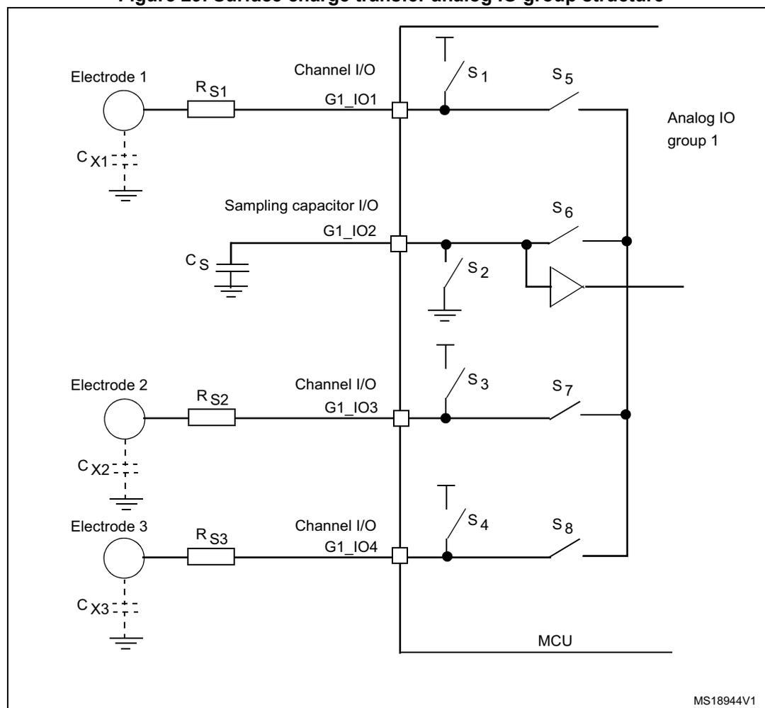
Note: \( G_x\_IO_y \) where \( x \) is the analog IO group number and \( y \) the GPIO number within the selected group.
For some specific needs (for example proximity detection), it is possible to enable, more than one channel per analog IO group simultaneously.
For the table of capacitive sensing I/Os refer to Table 41: I/O groups and selection on page 196 .
The surface charge transfer acquisition principle consists in charging an electrode capacitance ( \( C_X \) ) and transferring a part of the accumulated charge into a sampling capacitor ( \( C_S \) ). This sequence is repeated until the voltage across \( C_S \) reaches a given threshold (typically \( V_{IH} \) ). The number of charge transfers required to reach the threshold is a direct representation of the size of the electrode capacitance.
The Table 47 details the acquisition sequence of the capacitive sensing channel 1. The states 3 to 7 are repeated until the voltage across \( C_S \) reaches the given threshold. The same sequence applies to the acquisition of the other channels. The electrode serial resistor \( R_S \) allows improving the ESD immunity of the solution.
Table 47. Acquisition switching sequence summary
| State | S1 | S2 | S3 | S4 | S5 | S6 | S7 | S8 | State description |
|---|---|---|---|---|---|---|---|---|---|
| #1 | Open | Closed | Open | Open | Closed | Closed | Closed | Closed | Discharge all \( C_X \) and \( C_S \) |
| #2 | Open | Open | Open | Open | Open | Open | Open | Open | Dead time |
| #3 | Closed | Open | Open | Open | Open | Open | Open | Open | Charge \( C_{X1} \) |
| #4 | Open | Open | Open | Open | Open | Open | Open | Open | Dead time |
| #5 | Open | Open | Open | Open | Closed | Closed | Open | Open | Charge transfer from \( C_{X1} \) to \( C_S \) |
| #6 | Open | Open | Open | Open | Open | Open | Open | Open | Dead time |
| #7 | Open | Open | Open | Open | Open | Open | Open | Open | Measure voltage across \( C_S \) |
The voltage variation over the time of the sampling capacitor \( C_S \) is detailed below:
Figure 30. Sampling capacitor charge overview
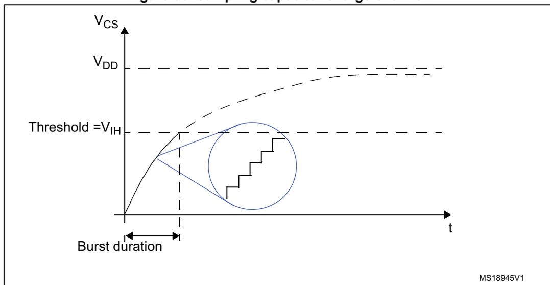
Figure 30 illustrates the charging of a sampling capacitor over time. The vertical axis represents the capacitor voltage \( V_{CS} \) , with horizontal dashed lines indicating the supply voltage \( V_{DD} \) and a threshold level \( V_{IH} \) . The horizontal axis represents time \( t \) . A dashed curve shows the exponential charging of the capacitor towards \( V_{DD} \) . A solid line represents the voltage during a 'Burst duration', showing a staircase-like approximation of the charging curve. A circle highlights the staircase part of the curve. The label MS18945V1 is in the bottom right corner.
9.3.2 Charge transfer acquisition management
In STM32L1xxxx devices, the acquisition can be managed in two modes:
- • Software mode: the GPIO port toggling and counting of the number of pulses is fully handled by the CPU.
- • Timer mode: the GPIO port toggling and counting of the number of pulses is handled by the timers (only in Cat.3, Cat.4, Cat.5 and Cat.6 devices).
Software mode acquisition
This mode uses the two following peripherals to control of the channel and sampling capacitor I/Os according to:
- • General purpose I/Os (see Section 7: General-purpose I/Os (GPIO) )
- • Routing interface (see Section 8: System configuration controller (SYSCFG) and routing interface (RI) on page 191 )
Table 48. Channel and sampling capacitor I/Os configuration summary
| State | Channel I/O configuration | Sampling capacitor I/O configuration |
|---|---|---|
| #1 | Output push-pull low | Output push-pull low |
| #2 | Input floating | Input floating with hysteresis disabled |
| #3 | Output push-pull high | |
| #4 | Input floating | Input floating with hysteresis disabled and analog switch closed |
| #5 | Input floating with analog switch closed | |
| #6 | Input floating | Input floating with hysteresis disabled |
| #7 |
Timer mode acquisition
This mode requires the use of the following peripherals:
- • General purpose I/Os (see Section 7 on page 171 )
- • Routing interface (see Section 8 on page 191 )
- • General-purpose timer 9 (see Section 18 on page 442 )
- • General-purpose timer 10 or 11 (see Section 18 on page 442 )
Figure 31. Timer mode acquisition logic
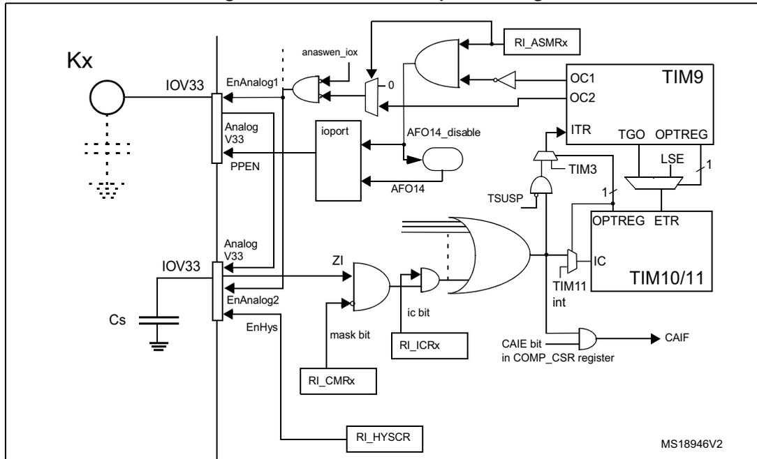
The diagram illustrates the internal logic for timer mode acquisition. It features two analog comparators, 'Analog V33', connected to an external pin 'Kx' through a switch 'Kx' and a sampling capacitor 'Cs'. The comparators are controlled by registers 'RI_ASMSRx', 'RI_ICRx', 'RI_CMRx', and 'RI_HYSCR'. The output of the comparators is connected to a timer block 'TIM9' and 'TIM10/11'. The logic includes various gates (AND, OR, NOT) and multiplexers to select between different input sources and control signals. Key signals include 'IOV33', 'EnAnalog1', 'EnAnalog2', 'PPEN', 'AFO14_disable', 'AFO14', 'TSUSP', 'TIM3', 'LSE', 'OPTREG', 'ETR', 'IC', 'TIM11 int', and 'CAIF' (indicated by a bit in the 'COMP_CSR' register). The diagram is labeled 'MS18946V2' in the bottom right corner.
Both timers are used to manage the GPIO port toggling which dramatically reduces the CPU load. TIM9 handles the charge transfer sequence generation by directly controlling the channel and sampling capacitor I/Os. TIM10 or 11 count the number of charge transfer cycles generated before an end of acquisition is detected on one of the enabled analog I/O groups.
The software sequence can be used to configure the different peripherals and to perform the acquisition.
Configuration steps:
- 1. Configure the I/O ports in alternate push-pull output mode, for the capacitive sensing channel I/Os to be acquired. Note that only one channel per group must be enabled at a time.
- 2. Configure the sampling capacitor I/Os in floating input mode with hysteresis disabled.
- 3. Configure TIM9 timer in center-aligned mode and generate PWM signals on OC1 and OC2. The typical frequency of the PWM signal is 250 KHz.
- 4. Configure TIM10 or 11 in slave mode with the clock signal generated by TIM9. In addition, IC1 must be enabled to capture the counter value on detection of an end of acquisition. Interrupt generation can be optionally enabled.
- 5. Enable TIM10 or 11.
- 6. Enable the control of analog switches of the channel and sampling capacitor I/Os by TIM9 using the RI_ASMRx registers (see Section 8.4: RI registers on page 201 ).
- 7. Identify the sampling capacitor I/Os using the registers RI_CICRx.
- 8. Start the acquisition by enabling TIM9.
Measurement steps:
At the end of acquisition on one sampling capacitor:
- 9. Clear the capture interrupt flag of TIM10 or 11 if interrupt generation enabled.
- 10. Read the IC register and save its contents in RAM.
- 11. Perform a XOR between RI_CMRx and GPIOx_IDR registers to determine which new channel(s) has (have) triggered an end of acquisition and update the corresponding channel information with the counter value.
- 12. Update the RI_CMRx registers to mask further end of acquisition detections on already detected channels. This automatically restarts TIM9.
9.4 Touch sensing library
In order to facilitate the development of a touch sensing solution based on STM32L1xxx devices, STMicroelectronics offers a STM32L1xx STMTouch sensing library that provides a complete robust C source-code solution. This firmware library is available as a free download from www.st.com . For information how to download the STM32L1xx STMTouch sensing library, contact your local ST representative.